EP3276830B1 - Halbleiterbauelement - Google Patents
Halbleiterbauelement Download PDFInfo
- Publication number
- EP3276830B1 EP3276830B1 EP17183557.2A EP17183557A EP3276830B1 EP 3276830 B1 EP3276830 B1 EP 3276830B1 EP 17183557 A EP17183557 A EP 17183557A EP 3276830 B1 EP3276830 B1 EP 3276830B1
- Authority
- EP
- European Patent Office
- Prior art keywords
- power supply
- supply circuit
- voltage
- resistors
- semiconductor device
- Prior art date
- Legal status (The legal status is an assumption and is not a legal conclusion. Google has not performed a legal analysis and makes no representation as to the accuracy of the status listed.)
- Active
Links
Images


Classifications
-
- H—ELECTRICITY
- H10—SEMICONDUCTOR DEVICES; ELECTRIC SOLID-STATE DEVICES NOT OTHERWISE PROVIDED FOR
- H10D—INORGANIC ELECTRIC SEMICONDUCTOR DEVICES
- H10D89/00—Aspects of integrated devices not covered by groups H10D84/00 - H10D88/00
- H10D89/60—Integrated devices comprising arrangements for electrical or thermal protection, e.g. protection circuits against electrostatic discharge [ESD]
- H10D89/601—Integrated devices comprising arrangements for electrical or thermal protection, e.g. protection circuits against electrostatic discharge [ESD] for devices having insulated gate electrodes, e.g. for IGFETs or IGBTs
- H10D89/811—Integrated devices comprising arrangements for electrical or thermal protection, e.g. protection circuits against electrostatic discharge [ESD] for devices having insulated gate electrodes, e.g. for IGFETs or IGBTs using FETs as protective elements
-
- B—PERFORMING OPERATIONS; TRANSPORTING
- B60—VEHICLES IN GENERAL
- B60Q—ARRANGEMENT OF SIGNALLING OR LIGHTING DEVICES, THE MOUNTING OR SUPPORTING THEREOF OR CIRCUITS THEREFOR, FOR VEHICLES IN GENERAL
- B60Q11/00—Arrangement of monitoring devices for devices provided for in groups B60Q1/00 - B60Q9/00
- B60Q11/005—Arrangement of monitoring devices for devices provided for in groups B60Q1/00 - B60Q9/00 for lighting devices, e.g. indicating if lamps are burning or not
-
- H—ELECTRICITY
- H02—GENERATION; CONVERSION OR DISTRIBUTION OF ELECTRIC POWER
- H02H—EMERGENCY PROTECTIVE CIRCUIT ARRANGEMENTS
- H02H3/00—Emergency protective circuit arrangements for automatic disconnection directly responsive to an undesired change from normal electric working condition with or without subsequent reconnection ; integrated protection
- H02H3/20—Emergency protective circuit arrangements for automatic disconnection directly responsive to an undesired change from normal electric working condition with or without subsequent reconnection ; integrated protection responsive to excess voltage
-
- H—ELECTRICITY
- H03—ELECTRONIC CIRCUITRY
- H03K—PULSE TECHNIQUE
- H03K17/00—Electronic switching or gating, i.e. not by contact-making and –breaking
- H03K17/08—Modifications for protecting switching circuit against overcurrent or overvoltage
- H03K17/081—Modifications for protecting switching circuit against overcurrent or overvoltage without feedback from the output circuit to the control circuit
- H03K17/0812—Modifications for protecting switching circuit against overcurrent or overvoltage without feedback from the output circuit to the control circuit by measures taken in the control circuit
-
- H—ELECTRICITY
- H05—ELECTRIC TECHNIQUES NOT OTHERWISE PROVIDED FOR
- H05B—ELECTRIC HEATING; ELECTRIC LIGHT SOURCES NOT OTHERWISE PROVIDED FOR; CIRCUIT ARRANGEMENTS FOR ELECTRIC LIGHT SOURCES, IN GENERAL
- H05B45/00—Circuit arrangements for operating light-emitting diodes [LED]
- H05B45/50—Circuit arrangements for operating light-emitting diodes [LED] responsive to malfunctions or undesirable behaviour of LEDs; responsive to LED life; Protective circuits
-
- H—ELECTRICITY
- H05—ELECTRIC TECHNIQUES NOT OTHERWISE PROVIDED FOR
- H05B—ELECTRIC HEATING; ELECTRIC LIGHT SOURCES NOT OTHERWISE PROVIDED FOR; CIRCUIT ARRANGEMENTS FOR ELECTRIC LIGHT SOURCES, IN GENERAL
- H05B47/00—Circuit arrangements for operating light sources in general, i.e. where the type of light source is not relevant
- H05B47/20—Responsive to malfunctions or to light source life; for protection
- H05B47/24—Circuit arrangements for protecting against overvoltage
-
- H—ELECTRICITY
- H10—SEMICONDUCTOR DEVICES; ELECTRIC SOLID-STATE DEVICES NOT OTHERWISE PROVIDED FOR
- H10D—INORGANIC ELECTRIC SEMICONDUCTOR DEVICES
- H10D89/00—Aspects of integrated devices not covered by groups H10D84/00 - H10D88/00
- H10D89/60—Integrated devices comprising arrangements for electrical or thermal protection, e.g. protection circuits against electrostatic discharge [ESD]
- H10D89/601—Integrated devices comprising arrangements for electrical or thermal protection, e.g. protection circuits against electrostatic discharge [ESD] for devices having insulated gate electrodes, e.g. for IGFETs or IGBTs
- H10D89/611—Integrated devices comprising arrangements for electrical or thermal protection, e.g. protection circuits against electrostatic discharge [ESD] for devices having insulated gate electrodes, e.g. for IGFETs or IGBTs using diodes as protective elements
-
- H—ELECTRICITY
- H02—GENERATION; CONVERSION OR DISTRIBUTION OF ELECTRIC POWER
- H02H—EMERGENCY PROTECTIVE CIRCUIT ARRANGEMENTS
- H02H9/00—Emergency protective circuit arrangements for limiting excess current or voltage without disconnection
- H02H9/02—Emergency protective circuit arrangements for limiting excess current or voltage without disconnection responsive to excess current
-
- H—ELECTRICITY
- H02—GENERATION; CONVERSION OR DISTRIBUTION OF ELECTRIC POWER
- H02H—EMERGENCY PROTECTIVE CIRCUIT ARRANGEMENTS
- H02H9/00—Emergency protective circuit arrangements for limiting excess current or voltage without disconnection
- H02H9/04—Emergency protective circuit arrangements for limiting excess current or voltage without disconnection responsive to excess voltage
- H02H9/042—Emergency protective circuit arrangements for limiting excess current or voltage without disconnection responsive to excess voltage comprising means to limit the absorbed power or indicate damaged over-voltage protection device
Definitions
- the present invention relates to a power supply circuit comprising a semiconductor device arranged to detect overvoltage.
- a switching driver which is used in a switching power supply circuit arranged to drive various loads including a light emitting element such as a light emitting diode (LED), is provided as a semiconductor device (IC).
- IC semiconductor device
- Many of the semiconductor devices have an overvoltage protection function of detecting overvoltage of an output voltage of the switching power supply circuit so as to protect the same.
- a voltage after dividing the output voltage by external resistors is usually input to a comparator inside the semiconductor device, so as to detect overvoltage.
- JP-A-2013-74679 discloses also a power supply circuit, however, only comprising a semiconductor device and a first resistor disposed externally of the semiconductor device according to the preamble of claim 1.
- the conventional structure has a problem that overvoltage cannot be detected when the external resistors that divide the output voltage is disconnected.
- set resistance values of the external resistors may be mistaken, and a set value of the overvoltage may exceed the withstand voltage of the semiconductor device.
- the output voltage may exceeds the withstand voltage of the semiconductor device, and the semiconductor device may be broken.
- a power supply circuit including a semiconductor device includes a first overvoltage detection unit including a first comparator arranged to output a first detection signal based on a first divided voltage after dividing an output voltage of a power supply circuit by first resistors disposed externally, and a second overvoltage detection unit including second resistors and a second comparator arranged to output a second detection signal based on a second divided voltage after dividing the output voltage by the second resistors.
- Fig. 1 is a diagram illustrating the entire configuration of a switching power supply circuit 60 arranged to drive an LED 70 according to an embodiment of the present invention.
- the switching power supply circuit 60 is a DC/DC converter including a semiconductor device 50 and an output stage 55.
- the output stage 55 disposed outside of the semiconductor device 50 includes a switching element Q1, a switching element Q2, a diode D1, a diode D2, a coil L1, a bootstrap capacitor Cb, an output capacitor C1, a resistor R1, and a resistor R2.
- the semiconductor device 50 functions as a switching driver IC arranged to switching-drive the switching elements Q1 and Q2. Note that the semiconductor device 50 can be also understood as an LED driver IC (light emitting element driving device).
- the semiconductor device 50 includes a logic unit 1, an internal power supply voltage generation unit 2, an under voltage lock out (UVLO) unit 3, a discharge circuit 4, an overvoltage detection unit 5, a driver control unit 6, an oscillator 7, a slope voltage generation unit 8, a comparator 9, a comparator 10, an error amplifier 11, a switch 12, a switch 13, an inverter 14, a dimming control unit 15, a duty setting unit 16, and a constant current control circuit 17. These structural elements are integrated.
- the semiconductor device 50 has external terminals T1 to T10 arranged to establish electrical connection with outside.
- the drain of the switching element Q1 constituted of an n-channel MOSFET is applied with an input voltage Vin, and the source thereof is connected to the cathode of the diode D1.
- the anode of the diode D1 is connected to an application terminal of a ground potential.
- the gate of the switching element Q1 is connected to the external terminal T2 of the semiconductor device 50.
- connection node between the switching element Q1 and the diode D1 is connected to one terminal of the coil L1, and the other terminal of the coil L1 is commonly connected to the anode of the diode D2 and the drain of the switching element Q2 constituted of an n-channel MOSFET.
- the source of the switching element Q2 is connected to the application terminal of the ground potential.
- the gate of the switching element Q2 is connected to the external terminal T3 of the semiconductor device 50.
- the cathode of the diode D2 is connected to one terminal of the output capacitor C1, and the other terminal of the output capacitor C1 is connected to the application terminal of the ground potential.
- connection node between the switching element Q1 and the coil L1 is connected to one terminal of the bootstrap capacitor Cb.
- the other terminal of the bootstrap capacitor Cb is connected to the external terminal T1 of the semiconductor device 50.
- An output voltage Vout is generated at the connection node between the cathode of the diode D2 and one terminal of the output capacitor C1.
- the resistor R1 and the resistor R2 for voltage division are connected in series between the connection node and the application terminal of the ground potential.
- a connection node PI between the resistor R1 and the resistor R2 is connected to the external terminal T4 of the semiconductor device 50.
- the connection node between the cathode of the diode D2 and one terminal of the output capacitor C1 is connected to an anode side of the LED 70.
- the cathode side of the LED 70 is connected to the external terminal T5 of the semiconductor device 50.
- connection node P1 between the resistor R1 and the resistor R2 is connected to a first inverting input terminal (-) of the error amplifier 11 via the external terminal T4 and the switch 12.
- the cathode side of the LED 70 is connected to a second inverting input terminal (-) of the error amplifier 11 via the external terminal T5 and the switch 13.
- the non-inverting input terminal (+) of the error amplifier 11 is applied with a first reference voltage Vrefl.
- the switch 12 is switched to on or off by a first switching signal SW1 sent from the logic unit 1.
- the switch 13 is switched to on or off by a logically inverted signal of the first switching signal SW1 from the inverter 14. In other words, depending on a logical level of the first switching signal SW1, the switch 12 is turned on while the switch 13 is turned off, or the switch 12 is turned off while the switch 13 is turned on.
- the error amplifier 11 amplifies a difference between the reference voltage Vrefl and one of a cathode voltage Vc of the LED 70 and a divided voltage Vdv1 after dividing the output voltage Vout by the resistor R1 and the resistor R2, so as to output an error voltage ERR.
- the error voltage ERR is input to the inverting input terminal (-) of the comparator 9.
- the slope voltage generation unit 8 generates a sawtooth or triangular slope voltage SL in synchronization with a clock signal output from the oscillator 7.
- the slope voltage SL is input to the non-inverting input terminal (+) of the comparator 9.
- the comparator 9 compares the error voltage ERR with the slope voltage SL so as to output a result of the comparison as a comparison signal SC to the driver control unit 6.
- the driver control unit 6 On the basis of the comparison signal SC, the driver control unit 6 generates a pulse-like pulse width modulation (PWM) signal Spwml or Spwm2 having an adjusted duty and outputs the same to a driver Dr1 or Dr2.
- PWM pulse-like pulse width modulation
- the driver Dr1 outputs a gate signal G1 to the gate of the switching element Q1 via the external terminal T2 so as to turn on the switching element Q1, the gate signal G1 having a voltage obtained by adding the input voltage Vin to a voltage generated in the bootstrap capacitor Cb when being charged by an internal power supply voltage Vreg (i.e., the internal power supply voltage Vreg minus the forward voltage of the diode Db).
- the driver Dr1 output the gate signal G1 having the ground potential to the gate of the switching element Q1 so as to turn off the switching element Q1.
- the driver Dr1 outputs the gate signal G1 in accordance with the PWM signal Spwml from the driver control unit 6 so as to switching-drive the switching element Q1.
- the driver Dr2 outputs a gate signal G2 having the internal power supply voltage Vreg or the ground potential to the gate of the switching element Q2 via the external terminal T3 so as to turn on or off the switching element Q2.
- the driver Dr2 outputs the gate signal G2 so as to switching-drive the switching element Q2 in accordance with the PWM signal Spwm2 from the driver control unit 6.
- the switching element Q2 when the switching element Q2 is maintained in the off state by the driver Dr2 while the switching element Q1 is on-off controlled by the driver Dr1, the input voltage Vin is stepped down so as to output the output voltage Vout as a step down mode.
- the switching element Q1 when the switching element Q1 is maintained at on state by the driver Dr1 while the switching element Q2 is on-off controlled by the driver Dr2, the input voltage Vin is stepped up so as to output the output voltage Vout as a step up mode.
- the cathode voltage Vc of the LED 70 is input to the error amplifier 11. Therefore, a feedback control is performed with the cathode voltage Vc as the feedback signal, duty of the PWM signal Spwml or Spwm2 is adjusted by the PWM control, and the cathode voltage Vc is controlled to be constant (second feedback control mode).
- the constant current control circuit 17 is a MOS transistor 171, a resistor 172, an error amplifier 173, a switch 174, a switch 175, an inverter 176, and a switch 177.
- the external terminal T5 to which the cathode side of the LED 70 is connected, is connected to the drain of the MOS transistor 171 constituted of the n-channel MOSFET.
- the source of the MOS transistor 171 is connected to one terminal of the resistor 172.
- the other terminal of the resistor 172 is connected to the application terminal of the ground potential.
- the connection node between the MOS transistor 171 and the resistor 172 is connected to the inverting input terminal (-) of the error amplifier 173 via the switch 175.
- the non-inverting input terminal (+) of the error amplifier 173 is applied with a second reference voltage Vref2.
- the output terminal of the error amplifier 173 is connected to the gate of the MOS transistor 171 via the switch 174.
- the connection node between the switch 174 and the MOS transistor 171 is connected to the application terminal of the ground potential via the switch 177.
- the switch 174 and the switch 175 are switched to on or off by the second switching signal SW2 sent from the logic unit 1.
- the switch 177 is switched to on or off by a logically inverted signal of a second switching signal SW2 from the inverter 176. In other words, on the basis of a logical level of the second switching signal SW2, the switches 174 and 175 are turned on while the switch 177 is turned off, or the switches 174 and 175 are turned off while the switch 177 is turned on.
- the error amplifier 173 When the switches 174 and 175 are turned on while the switch 177 is turned off by the second switching signal SW2, the error amplifier 173 is supplied with a current detection signal having a voltage obtained by converting current IL flowing in the LED 70 and the MOS transistor 171 by the resistor 172. Then, the error amplifier 173 outputs to the MOS transistor 171 a signal obtained by amplifying a difference between the current detection signal and the second reference voltage Vref2, so as to drive and control the MOS transistor 171. In this way, the constant current control is performed so as to maintain the constant current IL.
- a dimming signal DM as the PWM signal (pulse signal) having adjusted duty is externally input to the dimming control unit 15 via the external terminal T7.
- the dimming control unit 15 generates a dimming control signal DCR based on the dimming signal DM and outputs the same to the logic unit 1.
- the dimming brightness can be adjusted by the duty of the dimming signal DM.
- the duty setting unit 16 generates a duty set signal DS in accordance with a capacitance of a not-shown capacitor externally connected to the external terminal T8 and outputs the same to the logic unit 1.
- the duty set signal DS indicates a duty threshold value of the dimming signal DM.
- the logic unit 1 compares the duty of the dimming signal DM and the set threshold value based on the dimming control signal DCR and the duty set signal DS, and switches between the first feedback control mode and the second feedback control mode described above based on a result of the comparison.
- the logic unit 1 When it is determined that the dimming signal DM has a duty of the threshold value or more, the logic unit 1 turns off the switch 12 while turns on the switch 13 by the first switching signal SW1, so as to enable the second feedback control mode to maintain the cathode voltage Vc at a constant value.
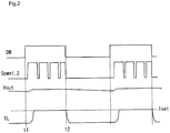
- An example of various signal waveforms is shown in Fig. 2 .
- the logic unit 1 when the dimming signal DM rises to High level at timing t1, the logic unit 1 turns on the switches 174 and 175 while turns off the switch 177 by the second switching signal SW2. In this way, the current IL rises to a set current Iset. In this case, the forward voltage generated in the LED 70 is increased. Therefore, if the output voltage Vout is approximately 30 V, for example, the cathode voltage Vc becomes approximately 1 V. If the first reference voltage Vrefl is 1 V, the PWM signal Spwml or Spwm2 is generated so that the cathode voltage Vc becomes constant at 1 V. In this way, the switching element Q1 or Q2 is on-off controlled.
- the logic unit 1 turns off the switches 174 and 175 while turns on the switch 177 by the second switching signal SW2, and hence the current IL is decreased to zero.
- the forward voltage generated in the LED 70 is decreased, and the cathode voltage Vc is increased to approximately 10 V in the above example. Therefore, the cathode voltage Vc becomes considerably higher than 1 V as the first reference voltage Vrefl, the PWM signal Spwml or Spwm2 is maintained at Low level, and the switching element Q1 or Q2 is maintained in the off state.
- the logic unit 1 enables the first feedback control mode in which the switch 12 is turned on while the switch 13 is turned off by the first switching signal SW1 so that the output voltage Vout is maintained at a constant value.
- An example of various signal waveforms in this case is illustrated in Fig. 3 .
- the logic unit 1 turns on the switches 174 and 175 while turns off the switch 177 by the second switching signal SW2, and the current IL rises to the set current Iset. Then, in the period while the current IL is controlled to be constant at the set current Iset, when the dimming signal DM falls at timing t12, the logic unit 1 turns off the switches 174 and 175 while turns on the switch 177 by the second switching signal SW2, and the current IL is decreased to zero. By repeating this operation, dark brightness of the LED 70 can be adjusted.
- the PWM signal Spwml or Spwm2 is always generated so that the output voltage Vout becomes constant.
- the PWM signal Spwml or Spwm2 is generated only in a short period while the dimming signal DM is High level, and hence the output voltage Vout cannot be maintained at a predetermined level. Therefore, if the dimming signal DM has a low duty, the first feedback control mode is enabled so that the output voltage Vout can be maintained at a predetermined level.
- the internal power supply voltage generation unit 2 is externally supplied with the input voltage Vin via the external terminal T9, and generates the internal power supply voltage Vreg based on the input voltage Vin.
- the internal power supply voltage Vreg is supplied to individual portions including the logic unit 1.
- the internal power supply voltage generation unit 2 raises the internal power supply voltage Vreg. Until the internal power supply voltage Vreg reaches a predetermined UVLO cancel voltage, a UVLO unit 3 maintains the logic unit 1 at a standby state. Further, when the internal power supply voltage Vreg reaches the UVLO cancel voltage, the UVLO unit 3 cancels the standby state of the logic unit 1. In this way, the semiconductor device 50 is activated.
- the internal power supply voltage generation unit 2 decreases the internal power supply voltage Vreg.
- the UVLO unit 3 sets the logic unit 1 to the standby state. In this way, the switching elements Q1 and Q2 is maintained in the off state, and the semiconductor device 50 becomes a power off state.
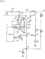
- Fig. 4 is a diagram illustrating a specific structural example of the discharge circuit 4 and the overvoltage detection unit 5.
- the discharge circuit 4 includes a MOS transistor 41 constituted of an n-channel MOSFET.
- the drain of the MOS transistor 41 is connected to a line Ln1 via the external terminal T10, the line Ln1 being connected to one terminal of the output capacitor C1 and generating the output voltage Vout.
- the source of the MOS transistor 41 is connected to the application terminal of the ground potential.
- the logic unit 1 supplies a gate signal to the gate of the MOS transistor 41, so as to switch on/off of the MOS transistor 41.
- the logic unit 1 When the logic unit 1 becomes the standby state by the UVLO unit 3 so that the semiconductor device 50 becomes the power off state, the logic unit 1 turns on the MOS transistor 41. In this way, charge is drawn from the output capacitor C1 via the external terminal T10 and the MOS transistor 41, and hence the output capacitor C1 is discharged. In this way, the output voltage Vout is securely 0 V. Note that the MOS transistor 41 is maintained at the off state after the semiconductor device 50 is activated.
- connection node PI between the resistor R1 and the resistor R2 is connected to the non-inverting input terminal (+) of the comparator 10 inside the semiconductor device 50 via the external terminal T4.
- the comparator 10 is constituted of a hysteresis comparator, and compares the divided voltage Vdv1 generated at the connection node PI with a first threshold value voltage or a second threshold value voltage (lower than the first threshold value voltage), so as to output a result of the comparison as a detection signal DET1 to the logic unit 1.
- the comparator 10 When the output voltage Vout becomes higher than a first overvoltage set value determined by the first threshold value voltage and resistance values of the resistors R1 and R2, the comparator 10 outputs the detection signal DET1 having High level. In other words, the comparator 10 functions as the overvoltage detection unit.
- the overvoltage detection unit 5 includes a MOS transistor 51 (switch) constituted of a p-channel MOSFET, a resistor 52, a resistor 53, and a comparator 54.
- the source of the MOS transistor 51 is connected to the line Ln1 via the external terminal T10.
- the resistor 52 and the resistor 53 are connected in series between the drain of the MOS transistor 51 and the application terminal of the ground potential.
- a connection node P2 between the resistor 52 and the resistor 53 is connected to the non-inverting input terminal (+) of the comparator 54.
- the logic unit 1 supplies a gate signal to the gate of the MOS transistor 51 so as to switch on/off of the MOS transistor 51.
- the MOS transistor 51 After the semiconductor device 50 is activated, the MOS transistor 51 is turned on. In addition, when the semiconductor device 50 becomes the power off state, the MOS transistor 51 is turned off. In this way, it is possible to prevent flowing of leak current from the line Ln1 via the MOS transistor 51 in the power off state.
- a divided voltage Vdv2 obtained by dividing the output voltage Vout by the resistor 52 and the resistor 53 is generated at the connection node P2.
- the comparator 54 is constituted of a hysteresis comparator, the divided voltage Vdv2 is compared with a third threshold value voltage or a fourth threshold value voltage (lower than the third threshold value voltage), so as to output a result of the comparison as a detection signal DET2 to the logic unit 1.
- the comparator 54 When the output voltage Vout becomes higher than a second overvoltage set value determined by the third threshold value voltage and resistance values of the resistors 52 and 53, the comparator 54 outputs the detection signal DET2 having High level.
- the second overvoltage set value is set to a value that is lower than a withstand voltage of the semiconductor device 50 and is quite close to the withstand voltage.
- the first overvoltage set value is set to a value equal to or lower than a predetermined overvoltage set value upper limit lower than the second overvoltage set value.
- the second overvoltage set value is set to 45 V
- the first overvoltage set value is set to a value equal to or lower than 40 V that is the overvoltage set value upper limit.
- the first overvoltage set value is set to 30 V or 25 V or other voltage according to application of the semiconductor device 50.
- the comparator 10 In the case where the resistors R1 and R2 as external resistors are in normal state, when the output voltage Vout reaches the first overvoltage set value before reaching the second overvoltage set value, the comparator 10 outputs the detection signal DET1 of High level so that the overvoltage is detected. When receiving this signal, the logic unit 1 controls to turn off the switching elements Q1 and Q2 so that overvoltage protection is performed. When the output voltage Vout falls so that the divided voltage Vdv1 becomes lower than the second threshold value voltage, the comparator 10 outputs the detection signal DET1 of Low level to the logic unit 1. When receiving this signal, the logic unit 1 controls to restart the switching control of the switching element Q1 or Q2.
- the comparator 54 outputs the detection signal DET2 of High level, and overvoltage can be detected.
- the logic unit 1 controls to turn off the switching elements Q1 and Q2 so that overvoltage protection is performed.
- the comparator 54 When the output voltage Vout falls so that the divided voltage Vdv2 becomes lower than the fourth threshold value voltage, the comparator 54 outputs the detection signal DET2 of Low level to the logic unit 1. When receiving this signal, the logic unit 1 controls to restart the switching control of the switching element Q1 or Q2.
- the resistors 52 and 53 included in the overvoltage detection unit 5 is configured inside the semiconductor device 50, there is almost no possibility of occurrence of abnormality such as disconnection or setting error of resistance values, unlike the external resistors R1 and R2.
- Fig. 4 also has an effect that there is no need to add an external terminal, because the external terminal T10 used for the discharge circuit 4 is also used for the overvoltage detection unit 5.
- a liquid crystal display device As an example of an application of the semiconductor device (switching power supply circuit) of the embodiment described above, a liquid crystal display device is described.
- a structural example of the liquid crystal display device is illustrated in Fig. 6 . Note that the structure illustrated in Fig. 6 is a so-called edge light type, but without limiting to this, a direct type may be adopted.
- a liquid crystal display device X illustrated in Fig. 6 includes a backlight 81, and a liquid crystal panel 82.
- the backlight 81 is an illumination device (an example of a light emission device) that illuminates the liquid crystal panel 82 from backside.
- the backlight 81 includes an LED light source unit 811, a light guide plate 812, a reflecting plate 813, and optical sheets 814.
- the LED light source unit 811 includes an LED and a substrate on which the LED is mounted. As a switching power supply circuit for use of driving the LED, the one according to the embodiment described above can be used.
- Light emitted from the LED light source unit 811 enters the light guide plate 812 from its side face.
- the light guide plate 812 made of an acrylic plate for example guides the entering light in the entire inside by total reflection, and outputs planar light from the surface on the side where the optical sheets 814 is disposed.
- the reflecting plate 813 reflects light leaking from the light guide plate 812 to the inside of the light guide plate 812.
- the optical sheets 814 includes a diffusion sheet, a lens sheet, and the like, for purposes of uniformizing and improving luminance of light illuminating the liquid crystal panel 82.
- the liquid crystal display device using the semiconductor device according to the embodiment described above is appropriately used for in-vehicle displays in particular.
- the technique for securely performing the overvoltage protection described above is laid down in ISO26262 that is an international standard concerning electric/electronic functional safety of a vehicle, and in this situation it is important in view of security.
- the in-vehicle display is disposed in a dashboard in front of a driver's seat like the in-vehicle displays Y illustrated in Fig. 7 , for example.
- the in-vehicle display Y can display various images such as car navigation information, a picked-up image of the rear of the vehicle, a speed meter, a tachometer, a fuel meter, a fuel economy meter, a shift position, and the like, so as to provide the user with various information.
Landscapes
- Engineering & Computer Science (AREA)
- Mechanical Engineering (AREA)
- Dc-Dc Converters (AREA)
Claims (11)
- Stromversorgungsschaltung (60), umfassend:1.1 ein Halbleiterbauelement (50); und1.2 erste Widerstände (R1, R2), die außerhalb des Halbleiterbauelements angeordnet sind;wobei das Halbleiterbauelement umfasst:1.3 eine erste Überspannungsdetektionseinheit (10), die einen ersten Komparator (10) umfasst, der dafür ausgelegt ist, ein erstes Detektionssignal (DET1) auf der Grundlage eines Vergleichs, mit einem ersten Schwellenspannungswert, einer ersten geteilten Spannung nach dem Teilen einer Ausgangsspannung der Stromversorgungsschaltung durch die ersten Widerstände auszugeben; und1.4 eine zweite Überspannungsdetektionseinheit (5), die zweite Widerstände (52, 53) und einem zweiten Komparator (54) umfasst, der dafür ausgelegt ist, ein zweites Detektionssignal (DET2) auf der Grundlage eines Vergleichs, mit einem zweiten Schwellenspannungswert, einer zweiten geteilten Spannung nach dem Teilen der Ausgangsspannung der Stromversorgungsschaltung durch die zweiten Widerstände auszugeben; wobei1.5 ein erster Überspannungs-Sollwert, der durch die erste Schwellenwertspannung und den Widerstandswert der ersten Widerstände bestimmt wird, niedriger ist als ein zweiter Überspannungs-Sollwert, der durch die zweite Schwellenwertspannung und den Widerstandswert der zweiten Widerstände bestimmt wird.
- Stromversorgungsschaltung nach Anspruch 1, wobei:das Halbleiterbauelement eine Logikeinheit (1) umfasst, die dafür ausgelegt ist, gemäß dem ersten Detektionssignal (DET1) und dem zweiten Detektionssignal (DET2) zu arbeiten, unddie Logikeinheit ein Schaltelement der Stromversorgungsschaltung ausschaltet, wenn das erste Detektionssignal oder das zweite Detektionssignal detektiert wird, um einen Überspannungsschutz zu realisieren.
- Stromversorgungsschaltung nach Anspruch 1 oder 2, des Weiteren umfassend:einen Ausgangskondensator (C1),wobeidas Halbleiterbauelement des Weiteren umfasst:einen externen Anschluss (T10), der mit dem Ausgangskondensator verbunden ist; undeine Entladeschaltung (4), die dafür ausgelegt ist, den Ausgangskondensator über den externen Anschluss zu entladen, unddie zweiten Widerstände mit dem externen Anschluss verbunden sind.
- Stromversorgungsschaltung nach Anspruch 1 oder 2, des Weiteren umfassend:einen Ausgangskondensator (C1),wobeidas Halbleiterbauelement des Weiteren umfasst:einen ersten externen Anschluss (T10), der mit dem in der Stromversorgungsschaltung angeordneten Ausgangskondensator verbunden ist;eine Entladeschaltung (4), die dafür ausgelegt ist, den Ausgangskondensator über den ersten externen Anschluss zu entladen; undeinen zweiten externen Anschluss (T11), der mit dem Ausgangskondensator verbunden ist, unddie zweiten Widerstände mit dem zweiten externen Anschluss verbunden sind.
- Stromversorgungsschaltung nach Anspruch 3 oder 4, wobei die Entladeschaltung aus einem MOS-Transistor (41) gebildet ist.
- Stromversorgungsschaltung nach einem der Ansprüche 1 bis 5, wobei die zweite Überspannungsdetektionseinheit des Weiteren einen Schalter (51) aufweist, der dafür ausgelegt ist, das Verbinden und Trennen eines Pfades zwischen einer Leitung, die die Ausgangsspannung erzeugt, und den zweiten Widerständen zu schalten.
- Stromversorgungsschaltung nach einem der Ansprüche 1 bis 6, wobei der zweite Komparator aus einem Hysteresekomparator (54) gebildet ist.
- Stromversorgungsschaltung nach einem der Ansprüche 1 bis 7, wobei die Stromversorgungsschaltung ein Leuchtelement als Last ansteuert.
- Leuchtvorrichtung, gekennzeichnet durch:die Stromversorgungsschaltung nach Anspruch 8; unddas Leuchtelement, das durch die Stromversorgungsschaltung angesteuert wird.
- Anzeigevorrichtung, welche die Leuchtvorrichtung nach Anspruch 9 umfasst.
- Anzeigevorrichtung nach Anspruch 10 als eine in ein Fahrzeug eingebaute Vorrichtung.
Applications Claiming Priority (1)
| Application Number | Priority Date | Filing Date | Title |
|---|---|---|---|
| JP2016147392A JP6762161B2 (ja) | 2016-07-27 | 2016-07-27 | 半導体装置 |
Publications (2)
| Publication Number | Publication Date |
|---|---|
| EP3276830A1 EP3276830A1 (de) | 2018-01-31 |
| EP3276830B1 true EP3276830B1 (de) | 2020-12-16 |
Family
ID=59501247
Family Applications (1)
| Application Number | Title | Priority Date | Filing Date |
|---|---|---|---|
| EP17183557.2A Active EP3276830B1 (de) | 2016-07-27 | 2017-07-27 | Halbleiterbauelement |
Country Status (3)
| Country | Link |
|---|---|
| US (1) | US10622349B2 (de) |
| EP (1) | EP3276830B1 (de) |
| JP (1) | JP6762161B2 (de) |
Families Citing this family (6)
| Publication number | Priority date | Publication date | Assignee | Title |
|---|---|---|---|---|
| JP7124803B2 (ja) * | 2019-07-24 | 2022-08-24 | 株式会社デンソー | 電源回路 |
| JP7354770B2 (ja) * | 2019-10-31 | 2023-10-03 | ブラザー工業株式会社 | 情報処理装置、情報処理装置の制御方法、及びプログラム |
| JP7519381B2 (ja) * | 2019-12-06 | 2024-07-19 | ローム株式会社 | 発光素子駆動装置 |
| US11632088B2 (en) | 2020-11-24 | 2023-04-18 | Elite Semiconductor Microelectronics Technology Inc. | Voltage converter and class-D amplifier |
| TWI755242B (zh) * | 2021-01-06 | 2022-02-11 | 晶豪科技股份有限公司 | 電壓轉換器以及d類放大器 |
| DE112022000704T5 (de) * | 2021-03-16 | 2023-11-09 | Rohm Co., Ltd. | Vorrichtung zur ansteuerung eines lichtemittierenden elements |
Family Cites Families (9)
| Publication number | Priority date | Publication date | Assignee | Title |
|---|---|---|---|---|
| JP2006211762A (ja) * | 2005-01-26 | 2006-08-10 | Sharp Corp | レギュレータ及びこれを備えた電子機器 |
| JP2006210219A (ja) * | 2005-01-31 | 2006-08-10 | Koito Mfg Co Ltd | 車両用灯具の点灯制御回路 |
| JP4685531B2 (ja) * | 2005-07-11 | 2011-05-18 | ローム株式会社 | 降圧型スイッチングレギュレータおよびその制御回路ならびにそれを用いた電子機器 |
| JP4582332B2 (ja) * | 2005-11-30 | 2010-11-17 | トヨタ自動車株式会社 | 電源電圧制御装置及びその制御方法 |
| WO2011013692A1 (ja) * | 2009-07-29 | 2011-02-03 | ローム株式会社 | Dc-dcコンバータ |
| JP5850612B2 (ja) * | 2010-12-09 | 2016-02-03 | ローム株式会社 | 発光素子の駆動回路、ならびにそれらを用いた発光装置、電子機器 |
| JP2012257444A (ja) * | 2011-05-13 | 2012-12-27 | Rohm Co Ltd | 昇圧型スイッチングレギュレータの制御回路およびそれを用いたスイッチングレギュレータならびに電子機器 |
| JP2013074679A (ja) | 2011-09-27 | 2013-04-22 | Denso Corp | 過電圧保護回路 |
| CN103269548B (zh) * | 2013-05-29 | 2015-07-08 | 成都芯源系统有限公司 | Led驱动电路系统,控制器及控制方法 |
-
2016
- 2016-07-27 JP JP2016147392A patent/JP6762161B2/ja active Active
-
2017
- 2017-07-26 US US15/660,438 patent/US10622349B2/en active Active
- 2017-07-27 EP EP17183557.2A patent/EP3276830B1/de active Active
Non-Patent Citations (1)
| Title |
|---|
| None * |
Also Published As
| Publication number | Publication date |
|---|---|
| JP6762161B2 (ja) | 2020-09-30 |
| US10622349B2 (en) | 2020-04-14 |
| US20180033785A1 (en) | 2018-02-01 |
| EP3276830A1 (de) | 2018-01-31 |
| JP2018019497A (ja) | 2018-02-01 |
Similar Documents
| Publication | Publication Date | Title |
|---|---|---|
| EP3276830B1 (de) | Halbleiterbauelement | |
| EP3276596B1 (de) | Halbleiterbauelement | |
| US10420196B2 (en) | Lighting circuit and vehicle lamp having the same | |
| EP3468303B1 (de) | Led-lampe mit ausfalldetektionsschaltung | |
| CN100525034C (zh) | 输出设备和具有该输出设备的电子装置 | |
| US20080136771A1 (en) | Backlight control circuit with primary and secondary switch units | |
| KR101875220B1 (ko) | Led 구동회로 | |
| US20140252950A1 (en) | Semiconductor light source lighting circuit and vehicular lamp | |
| GB2534098A (en) | Over-current protection circuit, LED backlight driving circuit and liquid crystal display | |
| CN102968960B (zh) | Led驱动器装置、lcd和驱动led背光单元的方法 | |
| US8203524B2 (en) | Light-emitting element driving circuit | |
| KR20160019934A (ko) | Led 백라이트 및 액정 디스플레이 | |
| JP7518856B2 (ja) | Led駆動装置、照明装置、および車載用表示装置 | |
| US20090302768A1 (en) | Inverter circuit for light source | |
| JP2007258671A (ja) | 発光ダイオードの駆動回路 | |
| EP3328163B1 (de) | Antriebsvorrichtung für ein lichtemittierendes element | |
| US20120154969A1 (en) | Overcurrent detection circuit of light emitting module | |
| JP5064762B2 (ja) | 放電ランプ・ドライブ装置 | |
| US20100033100A1 (en) | Backlight module control system and control method thereof | |
| KR100859034B1 (ko) | 백라이팅 인버터에서의 led 구동회로 | |
| CN115134968B (zh) | 用于驱动光源的电子系统和驱动光源的方法 | |
| KR102051733B1 (ko) | Led 구동회로 | |
| KR20210012664A (ko) | 차량 램프용 엠씨유의 고장 보상 장치 | |
| JP2021083309A (ja) | 発光素子駆動装置 | |
| JP2007318920A (ja) | スイッチング電源装置の制御方法、制御回路およびスイッチング電源装置 |
Legal Events
| Date | Code | Title | Description |
|---|---|---|---|
| PUAI | Public reference made under article 153(3) epc to a published international application that has entered the european phase |
Free format text: ORIGINAL CODE: 0009012 |
|
| STAA | Information on the status of an ep patent application or granted ep patent |
Free format text: STATUS: REQUEST FOR EXAMINATION WAS MADE |
|
| 17P | Request for examination filed |
Effective date: 20170727 |
|
| AK | Designated contracting states |
Kind code of ref document: A1 Designated state(s): AL AT BE BG CH CY CZ DE DK EE ES FI FR GB GR HR HU IE IS IT LI LT LU LV MC MK MT NL NO PL PT RO RS SE SI SK SM TR |
|
| AX | Request for extension of the european patent |
Extension state: BA ME |
|
| RBV | Designated contracting states (corrected) |
Designated state(s): AL AT BE BG CH CY CZ DE DK EE ES FI FR GB GR HR HU IE IS IT LI LT LU LV MC MK MT NL NO PL PT RO RS SE SI SK SM TR |
|
| R17P | Request for examination filed (corrected) |
Effective date: 20170727 |
|
| GRAP | Despatch of communication of intention to grant a patent |
Free format text: ORIGINAL CODE: EPIDOSNIGR1 |
|
| STAA | Information on the status of an ep patent application or granted ep patent |
Free format text: STATUS: GRANT OF PATENT IS INTENDED |
|
| INTG | Intention to grant announced |
Effective date: 20200909 |
|
| GRAS | Grant fee paid |
Free format text: ORIGINAL CODE: EPIDOSNIGR3 |
|
| GRAA | (expected) grant |
Free format text: ORIGINAL CODE: 0009210 |
|
| STAA | Information on the status of an ep patent application or granted ep patent |
Free format text: STATUS: THE PATENT HAS BEEN GRANTED |
|
| AK | Designated contracting states |
Kind code of ref document: B1 Designated state(s): AL AT BE BG CH CY CZ DE DK EE ES FI FR GB GR HR HU IE IS IT LI LT LU LV MC MK MT NL NO PL PT RO RS SE SI SK SM TR |
|
| REG | Reference to a national code |
Ref country code: GB Ref legal event code: FG4D |
|
| REG | Reference to a national code |
Ref country code: IE Ref legal event code: FG4D |
|
| REG | Reference to a national code |
Ref country code: DE Ref legal event code: R096 Ref document number: 602017029517 Country of ref document: DE |
|
| REG | Reference to a national code |
Ref country code: AT Ref legal event code: REF Ref document number: 1346525 Country of ref document: AT Kind code of ref document: T Effective date: 20210115 |
|
| PG25 | Lapsed in a contracting state [announced via postgrant information from national office to epo] |
Ref country code: GR Free format text: LAPSE BECAUSE OF FAILURE TO SUBMIT A TRANSLATION OF THE DESCRIPTION OR TO PAY THE FEE WITHIN THE PRESCRIBED TIME-LIMIT Effective date: 20210317 Ref country code: FI Free format text: LAPSE BECAUSE OF FAILURE TO SUBMIT A TRANSLATION OF THE DESCRIPTION OR TO PAY THE FEE WITHIN THE PRESCRIBED TIME-LIMIT Effective date: 20201216 Ref country code: NO Free format text: LAPSE BECAUSE OF FAILURE TO SUBMIT A TRANSLATION OF THE DESCRIPTION OR TO PAY THE FEE WITHIN THE PRESCRIBED TIME-LIMIT Effective date: 20210316 Ref country code: RS Free format text: LAPSE BECAUSE OF FAILURE TO SUBMIT A TRANSLATION OF THE DESCRIPTION OR TO PAY THE FEE WITHIN THE PRESCRIBED TIME-LIMIT Effective date: 20201216 |
|
| REG | Reference to a national code |
Ref country code: AT Ref legal event code: MK05 Ref document number: 1346525 Country of ref document: AT Kind code of ref document: T Effective date: 20201216 |
|
| REG | Reference to a national code |
Ref country code: NL Ref legal event code: MP Effective date: 20201216 |
|
| PG25 | Lapsed in a contracting state [announced via postgrant information from national office to epo] |
Ref country code: BG Free format text: LAPSE BECAUSE OF FAILURE TO SUBMIT A TRANSLATION OF THE DESCRIPTION OR TO PAY THE FEE WITHIN THE PRESCRIBED TIME-LIMIT Effective date: 20210316 Ref country code: LV Free format text: LAPSE BECAUSE OF FAILURE TO SUBMIT A TRANSLATION OF THE DESCRIPTION OR TO PAY THE FEE WITHIN THE PRESCRIBED TIME-LIMIT Effective date: 20201216 Ref country code: SE Free format text: LAPSE BECAUSE OF FAILURE TO SUBMIT A TRANSLATION OF THE DESCRIPTION OR TO PAY THE FEE WITHIN THE PRESCRIBED TIME-LIMIT Effective date: 20201216 |
|
| PG25 | Lapsed in a contracting state [announced via postgrant information from national office to epo] |
Ref country code: NL Free format text: LAPSE BECAUSE OF FAILURE TO SUBMIT A TRANSLATION OF THE DESCRIPTION OR TO PAY THE FEE WITHIN THE PRESCRIBED TIME-LIMIT Effective date: 20201216 Ref country code: HR Free format text: LAPSE BECAUSE OF FAILURE TO SUBMIT A TRANSLATION OF THE DESCRIPTION OR TO PAY THE FEE WITHIN THE PRESCRIBED TIME-LIMIT Effective date: 20201216 |
|
| REG | Reference to a national code |
Ref country code: LT Ref legal event code: MG9D |
|
| PG25 | Lapsed in a contracting state [announced via postgrant information from national office to epo] |
Ref country code: SK Free format text: LAPSE BECAUSE OF FAILURE TO SUBMIT A TRANSLATION OF THE DESCRIPTION OR TO PAY THE FEE WITHIN THE PRESCRIBED TIME-LIMIT Effective date: 20201216 Ref country code: PT Free format text: LAPSE BECAUSE OF FAILURE TO SUBMIT A TRANSLATION OF THE DESCRIPTION OR TO PAY THE FEE WITHIN THE PRESCRIBED TIME-LIMIT Effective date: 20210416 Ref country code: RO Free format text: LAPSE BECAUSE OF FAILURE TO SUBMIT A TRANSLATION OF THE DESCRIPTION OR TO PAY THE FEE WITHIN THE PRESCRIBED TIME-LIMIT Effective date: 20201216 Ref country code: SM Free format text: LAPSE BECAUSE OF FAILURE TO SUBMIT A TRANSLATION OF THE DESCRIPTION OR TO PAY THE FEE WITHIN THE PRESCRIBED TIME-LIMIT Effective date: 20201216 Ref country code: LT Free format text: LAPSE BECAUSE OF FAILURE TO SUBMIT A TRANSLATION OF THE DESCRIPTION OR TO PAY THE FEE WITHIN THE PRESCRIBED TIME-LIMIT Effective date: 20201216 Ref country code: EE Free format text: LAPSE BECAUSE OF FAILURE TO SUBMIT A TRANSLATION OF THE DESCRIPTION OR TO PAY THE FEE WITHIN THE PRESCRIBED TIME-LIMIT Effective date: 20201216 Ref country code: CZ Free format text: LAPSE BECAUSE OF FAILURE TO SUBMIT A TRANSLATION OF THE DESCRIPTION OR TO PAY THE FEE WITHIN THE PRESCRIBED TIME-LIMIT Effective date: 20201216 |
|
| PG25 | Lapsed in a contracting state [announced via postgrant information from national office to epo] |
Ref country code: AT Free format text: LAPSE BECAUSE OF FAILURE TO SUBMIT A TRANSLATION OF THE DESCRIPTION OR TO PAY THE FEE WITHIN THE PRESCRIBED TIME-LIMIT Effective date: 20201216 Ref country code: PL Free format text: LAPSE BECAUSE OF FAILURE TO SUBMIT A TRANSLATION OF THE DESCRIPTION OR TO PAY THE FEE WITHIN THE PRESCRIBED TIME-LIMIT Effective date: 20201216 |
|
| REG | Reference to a national code |
Ref country code: DE Ref legal event code: R097 Ref document number: 602017029517 Country of ref document: DE |
|
| PG25 | Lapsed in a contracting state [announced via postgrant information from national office to epo] |
Ref country code: IS Free format text: LAPSE BECAUSE OF FAILURE TO SUBMIT A TRANSLATION OF THE DESCRIPTION OR TO PAY THE FEE WITHIN THE PRESCRIBED TIME-LIMIT Effective date: 20210416 |
|
| PLBE | No opposition filed within time limit |
Free format text: ORIGINAL CODE: 0009261 |
|
| STAA | Information on the status of an ep patent application or granted ep patent |
Free format text: STATUS: NO OPPOSITION FILED WITHIN TIME LIMIT |
|
| PG25 | Lapsed in a contracting state [announced via postgrant information from national office to epo] |
Ref country code: IT Free format text: LAPSE BECAUSE OF FAILURE TO SUBMIT A TRANSLATION OF THE DESCRIPTION OR TO PAY THE FEE WITHIN THE PRESCRIBED TIME-LIMIT Effective date: 20201216 Ref country code: AL Free format text: LAPSE BECAUSE OF FAILURE TO SUBMIT A TRANSLATION OF THE DESCRIPTION OR TO PAY THE FEE WITHIN THE PRESCRIBED TIME-LIMIT Effective date: 20201216 |
|
| 26N | No opposition filed |
Effective date: 20210917 |
|
| PG25 | Lapsed in a contracting state [announced via postgrant information from national office to epo] |
Ref country code: DK Free format text: LAPSE BECAUSE OF FAILURE TO SUBMIT A TRANSLATION OF THE DESCRIPTION OR TO PAY THE FEE WITHIN THE PRESCRIBED TIME-LIMIT Effective date: 20201216 |
|
| PG25 | Lapsed in a contracting state [announced via postgrant information from national office to epo] |
Ref country code: ES Free format text: LAPSE BECAUSE OF FAILURE TO SUBMIT A TRANSLATION OF THE DESCRIPTION OR TO PAY THE FEE WITHIN THE PRESCRIBED TIME-LIMIT Effective date: 20201216 |
|
| PG25 | Lapsed in a contracting state [announced via postgrant information from national office to epo] |
Ref country code: SI Free format text: LAPSE BECAUSE OF FAILURE TO SUBMIT A TRANSLATION OF THE DESCRIPTION OR TO PAY THE FEE WITHIN THE PRESCRIBED TIME-LIMIT Effective date: 20201216 |
|
| REG | Reference to a national code |
Ref country code: CH Ref legal event code: PL |
|
| GBPC | Gb: european patent ceased through non-payment of renewal fee |
Effective date: 20210727 |
|
| PG25 | Lapsed in a contracting state [announced via postgrant information from national office to epo] |
Ref country code: MC Free format text: LAPSE BECAUSE OF FAILURE TO SUBMIT A TRANSLATION OF THE DESCRIPTION OR TO PAY THE FEE WITHIN THE PRESCRIBED TIME-LIMIT Effective date: 20201216 |
|
| REG | Reference to a national code |
Ref country code: BE Ref legal event code: MM Effective date: 20210731 |
|
| PG25 | Lapsed in a contracting state [announced via postgrant information from national office to epo] |
Ref country code: LI Free format text: LAPSE BECAUSE OF NON-PAYMENT OF DUE FEES Effective date: 20210731 Ref country code: GB Free format text: LAPSE BECAUSE OF NON-PAYMENT OF DUE FEES Effective date: 20210727 Ref country code: CH Free format text: LAPSE BECAUSE OF NON-PAYMENT OF DUE FEES Effective date: 20210731 |
|
| PG25 | Lapsed in a contracting state [announced via postgrant information from national office to epo] |
Ref country code: IS Free format text: LAPSE BECAUSE OF FAILURE TO SUBMIT A TRANSLATION OF THE DESCRIPTION OR TO PAY THE FEE WITHIN THE PRESCRIBED TIME-LIMIT Effective date: 20210416 Ref country code: LU Free format text: LAPSE BECAUSE OF NON-PAYMENT OF DUE FEES Effective date: 20210727 Ref country code: FR Free format text: LAPSE BECAUSE OF NON-PAYMENT OF DUE FEES Effective date: 20210731 |
|
| PG25 | Lapsed in a contracting state [announced via postgrant information from national office to epo] |
Ref country code: IE Free format text: LAPSE BECAUSE OF NON-PAYMENT OF DUE FEES Effective date: 20210727 Ref country code: BE Free format text: LAPSE BECAUSE OF NON-PAYMENT OF DUE FEES Effective date: 20210731 |
|
| PG25 | Lapsed in a contracting state [announced via postgrant information from national office to epo] |
Ref country code: HU Free format text: LAPSE BECAUSE OF FAILURE TO SUBMIT A TRANSLATION OF THE DESCRIPTION OR TO PAY THE FEE WITHIN THE PRESCRIBED TIME-LIMIT; INVALID AB INITIO Effective date: 20170727 |
|
| P01 | Opt-out of the competence of the unified patent court (upc) registered |
Effective date: 20230512 |
|
| PG25 | Lapsed in a contracting state [announced via postgrant information from national office to epo] |
Ref country code: CY Free format text: LAPSE BECAUSE OF FAILURE TO SUBMIT A TRANSLATION OF THE DESCRIPTION OR TO PAY THE FEE WITHIN THE PRESCRIBED TIME-LIMIT Effective date: 20201216 |
|
| PG25 | Lapsed in a contracting state [announced via postgrant information from national office to epo] |
Ref country code: MK Free format text: LAPSE BECAUSE OF FAILURE TO SUBMIT A TRANSLATION OF THE DESCRIPTION OR TO PAY THE FEE WITHIN THE PRESCRIBED TIME-LIMIT Effective date: 20201216 |
|
| PG25 | Lapsed in a contracting state [announced via postgrant information from national office to epo] |
Ref country code: MT Free format text: LAPSE BECAUSE OF FAILURE TO SUBMIT A TRANSLATION OF THE DESCRIPTION OR TO PAY THE FEE WITHIN THE PRESCRIBED TIME-LIMIT Effective date: 20201216 |
|
| PGFP | Annual fee paid to national office [announced via postgrant information from national office to epo] |
Ref country code: DE Payment date: 20250604 Year of fee payment: 9 |
|
| PG25 | Lapsed in a contracting state [announced via postgrant information from national office to epo] |
Ref country code: TR Free format text: LAPSE BECAUSE OF FAILURE TO SUBMIT A TRANSLATION OF THE DESCRIPTION OR TO PAY THE FEE WITHIN THE PRESCRIBED TIME-LIMIT Effective date: 20201216 |