EP3280065A1 - Procédé et système pour étalonner la phase supportés par des données de garniture en usine - Google Patents
Procédé et système pour étalonner la phase supportés par des données de garniture en usine Download PDFInfo
- Publication number
- EP3280065A1 EP3280065A1 EP17183142.3A EP17183142A EP3280065A1 EP 3280065 A1 EP3280065 A1 EP 3280065A1 EP 17183142 A EP17183142 A EP 17183142A EP 3280065 A1 EP3280065 A1 EP 3280065A1
- Authority
- EP
- European Patent Office
- Prior art keywords
- phase
- communications device
- trim
- phase offset
- rssi
- Prior art date
- Legal status (The legal status is an assumption and is not a legal conclusion. Google has not performed a legal analysis and makes no representation as to the accuracy of the status listed.)
- Granted
Links
Images




Classifications
-
- H—ELECTRICITY
- H04—ELECTRIC COMMUNICATION TECHNIQUE
- H04B—TRANSMISSION
- H04B5/00—Near-field transmission systems, e.g. inductive or capacitive transmission systems
- H04B5/70—Near-field transmission systems, e.g. inductive or capacitive transmission systems specially adapted for specific purposes
-
- H—ELECTRICITY
- H04—ELECTRIC COMMUNICATION TECHNIQUE
- H04B—TRANSMISSION
- H04B5/00—Near-field transmission systems, e.g. inductive or capacitive transmission systems
- H04B5/20—Near-field transmission systems, e.g. inductive or capacitive transmission systems characterised by the transmission technique; characterised by the transmission medium
- H04B5/24—Inductive coupling
-
- H—ELECTRICITY
- H04—ELECTRIC COMMUNICATION TECHNIQUE
- H04W—WIRELESS COMMUNICATION NETWORKS
- H04W4/00—Services specially adapted for wireless communication networks; Facilities therefor
- H04W4/80—Services using short range communication, e.g. near-field communication [NFC], radio-frequency identification [RFID] or low energy communication
-
- H—ELECTRICITY
- H04—ELECTRIC COMMUNICATION TECHNIQUE
- H04B—TRANSMISSION
- H04B17/00—Monitoring; Testing
- H04B17/20—Monitoring; Testing of receivers
- H04B17/21—Monitoring; Testing of receivers for calibration; for correcting measurements
-
- H—ELECTRICITY
- H04—ELECTRIC COMMUNICATION TECHNIQUE
- H04B—TRANSMISSION
- H04B17/00—Monitoring; Testing
- H04B17/30—Monitoring; Testing of propagation channels
- H04B17/309—Measuring or estimating channel quality parameters
- H04B17/318—Received signal strength
-
- H—ELECTRICITY
- H04—ELECTRIC COMMUNICATION TECHNIQUE
- H04B—TRANSMISSION
- H04B5/00—Near-field transmission systems, e.g. inductive or capacitive transmission systems
- H04B5/70—Near-field transmission systems, e.g. inductive or capacitive transmission systems specially adapted for specific purposes
- H04B5/73—Near-field transmission systems, e.g. inductive or capacitive transmission systems specially adapted for specific purposes for taking measurements, e.g. using sensing coils
-
- H—ELECTRICITY
- H04—ELECTRIC COMMUNICATION TECHNIQUE
- H04B—TRANSMISSION
- H04B5/00—Near-field transmission systems, e.g. inductive or capacitive transmission systems
- H04B5/70—Near-field transmission systems, e.g. inductive or capacitive transmission systems specially adapted for specific purposes
- H04B5/77—Near-field transmission systems, e.g. inductive or capacitive transmission systems specially adapted for specific purposes for interrogation
-
- H—ELECTRICITY
- H04—ELECTRIC COMMUNICATION TECHNIQUE
- H04L—TRANSMISSION OF DIGITAL INFORMATION, e.g. TELEGRAPHIC COMMUNICATION
- H04L7/00—Arrangements for synchronising receiver with transmitter
- H04L7/04—Speed or phase control by synchronisation signals
-
- H—ELECTRICITY
- H04—ELECTRIC COMMUNICATION TECHNIQUE
- H04B—TRANSMISSION
- H04B5/00—Near-field transmission systems, e.g. inductive or capacitive transmission systems
- H04B5/40—Near-field transmission systems, e.g. inductive or capacitive transmission systems characterised by components specially adapted for near-field transmission
- H04B5/45—Transponders
Definitions
- the described embodiments relate generally to method and system to calibrate phase in a near field communication (NFC) system, and more particularly to method and system to calibrate phase supported by factory trim data in a near field communication (NFC) system.
- NFC near field communication
- NFC Near Field Communication
- a typical NFC based system consists of a NFC reader (e.g., Point of Sale terminal) and a NFC device, typically a NFC enabled card or a mobile phone.
- NFC reader e.g., Point of Sale terminal
- NFC device typically a NFC enabled card or a mobile phone.
- a NFC device typically can be configured for either passive load modulation (PLM) or active load modulation (ALM).
- PLM passive load modulation
- ALM active load modulation
- components for implementing ALM in a transponder e.g., a mobile device
- PLM passive load modulation
- ALM active load modulation
- components for implementing ALM in a transponder can be more compact and, because the transponder utilizes a power source to generate a magnetic field rather than just modulate a magnetic field created by a reader, an ALM transponder can have greater communication distance than a PLM transponder.
- the NFC enabled device In order to perform a transaction using a NFC enabled device and a NFC reader, the NFC enabled device is brought near the NFC reader.
- the communication between the NFC enabled device and the NFC reader may fail if the NFC reader fails to properly demodulate the signal from the NFC enabled device. Such failures may occur if the NFC enabled device is not properly aligned with the NFC reader or if the NFC enabled device is not within a certain distance range from the NFC reader.
- the present invention provides for a method and system to compensate phase offset caused by the IC (integrated circuit) by making use of factory measurement stored as trim-data in the IC.
- the trim-data is mapped to the actual platform environment such that the respective phase offset can be compensated.
- An important point of this invention is to create and store the trim-data referenced to an artificial (virtual) platform and the respective set of artificial (virtual) parameters.
- an efficient and simple scaling of the real and actual system platform parameters to the virtual trim-codes needs to be applied (e.g., by scaling).
- the present invention provides for a method for determining and applying phase offset to a communications device that communicates via inductive coupling, the method comprising: (a) measuring a received signal strength indicator (RSSI) value for the communications device; (b) using a platform specific mapping table to determine an index of phase trim corresponding to the measured RSSI value for the communications device; (c) using a reference phase trim data to determine a phase offset corresponding to the index of phase trim; and (d) applying the phase offset to the communications device.
- RSSI received signal strength indicator
- the reference phase trim data maps each phase offset to each own index.
- the reference phase trim data is measured and stored for each individual communications device, wherein each individual communications device has its own individualized reference phase trim data.
- the platform specific mapping table maps each RSSI value to each own index of phase trim.
- the platform specific mapping table is the same for all communications device belonging to the same type of communications devices, wherein each individual communications device belonging to the same type of communications devices does not have its own individualized platform specific mapping table.
- the reference phase trim data is stored in a protected memory area not accessible to a user.
- the user is a customer.
- the platform specific mapping table is stored in an open memory area accessible to a user.
- the method further comprises: (e) determining a TX (transmitter) phase setting; (f) determining a customer phase offset; and (g) applying the phase offset, the TX (transmitter) phase setting, and the customer phase offset to the communications device.
- the TX (transmitter) phase setting is a phase setting used for TX (transmitter) referenced to a phase detected at RX (receiver), wherein the customer phase offset is a phase offset that is considered a part to part variation of customer boards due to matching network and antenna.
- the customer phase offset is a static value evaluated once in a customer production test.
- the present invention also provides for a method for determining and applying phase offset to a communications device that communicates via inductive coupling, the method comprising: (a) measuring a received signal strength indicator (RSSI) value for the communications device; (b) using a platform specific mapping function to determine a variable of phase trim corresponding to the measured RSSI value for the communications device; (c) using a reference phase trim data to determine a phase offset corresponding to the variable of phase trim; and (d) applying the phase offset to the communications device.
- RSSI received signal strength indicator
- the reference phase trim data maps each phase offset to each own variable.
- the reference phase trim data is measured and stored for each individual communications device, wherein each individual communications device has its own individualized reference phase trim data.
- the platform specific mapping function maps each RSSI value to each own variable of phase trim.
- the platform specific mapping function is the same for all communications device belonging to the same type of communications devices, wherein each individual communications device belonging to the same type of communications devices does not have its own individualized platform specific mapping function.
- the reference phase trim data is stored in a protected memory area not accessible to a user.
- the platform specific mapping function is stored in an open memory area accessible to a user.
- the present invention further provides for a method for determining and applying phase offset to a communications device that communicates via inductive coupling, the method comprising: (a) measuring a characteristic parameter for the communications device; (b) using a platform specific mapping table or function to determine an index or variable of phase trim corresponding to the measured characteristic parameter for the communications device; (c) using a reference phase trim data to determine a phase offset corresponding to the index or variable of phase trim; and (d) applying the phase offset to the communications device.
- the characteristic parameter is a received signal strength indicator (RSSI) value, wherein the RSSI value corresponds to a field strength of inductive coupling.
- RSSI received signal strength indicator
- the present invention can also provide for a computer program product encoded in a non-transitory computer readable medium for determining and applying phase offset to a communications device that communicates via inductive coupling, the computer program product comprising: (a) computer code for measuring a characteristic parameter for the communications device; (b) computer code for using a platform specific mapping table or function to determine an index or variable of phase trim corresponding to the measured characteristic parameter for the communications device; (c) computer code for using a reference phase trim data to determine a phase offset corresponding to the index or variable of phase trim; and (d) computer code for applying the phase offset to the communications device.
- ALM Active load modulation
- ALM is state of the art for all mobile NFC solution in the market.
- ALM is an actively sending of 13.56MHz signal modulated according to standards for Type A/B/F. This grants a huge benefit in generated signal strength and allows for the use of smaller antennas by fulfilling the required standards like NFC Forum, ISO 14443, EMVCo, etc. with respect to load modulation amplitude parameter.
- a dedicated initial phase can be defined for the card response for all cases of ALM.
- the initial phase setting can be used to optimize the load modulation amplitude as shown in FIG. 1 for different coupling positions shown as "110", “120", “130”, and "140".
- the x-axis can represent the initial phase setting in degrees (i.e., phase of ALM versus TX CW (transmitter carrier wave) signal phase).
- FIG. 1 shows the load modulation amplitude peaking for some phase values. Therefore, in some embodiments, the phase can be used to optimize the load modulation amplitude.
- the transmitter (TX) phase (phase relation from reader field as seen on the RX and the phase of the carrier at the TX) of the NFC system depends on multiple system and/or environmental parameters/conditions (e.g., field strength, detuning/coupling condition, antenna geometries, IC (PVT) (integrated circuit - process, voltage and temperature), matching network (topology, (7), protocol, data-rate, retransmission, reconfiguration, timings, applications, etc.
- environmental parameters/conditions e.g., field strength, detuning/coupling condition, antenna geometries, IC (PVT) (integrated circuit - process, voltage and temperature), matching network (topology, 7), protocol, data-rate, retransmission, reconfiguration, timings, applications, etc.
- the TX (transmitter) phase that can be used for a platform is defined by a measurement campaign with multiple reader terminals. There is a TX phase range that gives a passing communication for all readers (as, for example, defined in IOT (Interoperability Test) certification).
- the main challenge for compensating the phase is to:
- ATE automated test equipment
- An important point of this invention is to create and store the trim-data referenced to an artificial (virtual) platform and the respective set of artificial (virtual) parameters.
- an efficient and simple scaling of the real and actual system platform parameters to the virtual trim-codes needs to be applied (e.g., by scaling).
- the receiver 200 comprises I/Q mixer 220, amplifier 230, filtering 240, A/D converter 250, and a signal demodulator 260.
- the receiver receives a RF input 210 to the I/Q mixer 220 and generates a BB (baseband) output 270 from the signal demodulator 260.
- BB baseband
- FIG. 3 gives an overview of a method for calculating a phase, in accordance with some example embodiments. There are several contributors to a calibrated phase 370, which is finally dialed into the system.
- the initial phase setting 350 is the target programmed phase. This is an absolute phase value.
- the customer phase offset 360 is a phase offset that considers part to part variation of customer boards due to matching network, antenna, etc. - basically contributors outside the IC and hence only known to the IC by this parameter. This is a static value evaluated once in a customer production test.
- RSSI 330 is the dynamically measured metric that is equivalent to the input voltage level. As the actual input voltage value depends on platform parameters and RSSI trimming, the RSSI does not give the absolute VRX voltage. Note that input voltage level and in turn RSSI 330 is dependent on the field strength H (310)
- the system scaling factor 320 is a correction of the platform RSSI to the absolute VRX voltage.
- phase trim data (or in some embodiments, the phase trim table) can be kept target platform independent, while the platform dependency can be addressed by the system scaling.
- phase trim data is shown as Phase Trim ph ic (RSSI) 340.
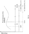
- FIG. 4 shows the phase behavior of the system/IC (which is shown as an arbitrary shape in this example), which actually depends on the input voltage Vin.
- the input signal can be quantified by field-strength or RSSI or some other characteristic parameter.
- field-strength is shown as H_1
- RSSI is shown as RSSI_1.
- H_2 field-strength
- RSSI_2 is shown as RSSI_2.
- FIG. 5 shows the phase behavior of a system/IC (integrated circuit), as the field strength (H)/RSSI from the respective platforms is mapped to an invariant reference input, in accordance with some example embodiments.
- the field-strength (H_i)/RSSI (RSSI_i)/... from the respective platform i has been mapped to an invariant reference input H_ref/RSSI_ref.
- field-strength H_1/RSSI_1 is associated with platform 1.
- Field-strength H_2/RSSI_2 is associated with platform 2.
- Field-strength H_ref/RSSI_ref is associated with an invariant reference platform.
- FIG. 5 shows the phase behavior of a system/IC (integrated circuit), as the field strength (H)/RSSI from the respective platforms is mapped to an invariant reference input, in accordance with some example embodiments.
- the phase behavior of the IC/system is referenced to a virtual reference scale in terms of field-strength/RSSI, which in turn is used as basis, which the platform metrics (H, RSSI) is mapped to.
- Table 1A Reference Platform 1 Platform 2 H_ref (A/m) Phase Offset (deg) H_ref (A/m) Phase Offset (deg) H_ref (A/m) Phase Offset (deg) 1 phi_1 1.1 phi_1 0.75 phi_1 2 phi_2 2.2 phi_2 1.5 phi_2 3 ... 3.3 ... 2.25 ...
- phase offsets phi_1, phi_2, ... are referred to different field-strength/RSSI depending on the actual platform.
- Table 1A and 1B show the mapping between phase to be compensated (phi_i) and the respective parameter to be selected (i.e., field strength H for Table 1A and RSSI for Table 1B). Note that the values are examples only for illustrative purposes.
- mapping table (or function) as shown in Table 2.
- This function allows for the use of the same scale for the input (in this example in terms of field-strength, but in another embodiment it could be RSSI as well) or an arbitrary scale.
- the important part of the mapping table is that the scale per platform maps (tabular or function) to the index of the actual trim-table (the reference table).
- the reference table can be considered as a trim-data table that is filled with data during a factory test (of the IC) and is fully separated and independent of the platform specifics.
- the information is generated in the following sequence.
- the first step is generation of the compensation table, which is referred to a reference system as shown in Table 3.
- This table is generated on a test system by the ATE (automated test equipment).
- this table may be stored in a "trim-area", a protected memory in a non-volatile memory that is persistent and will not be changed later on.
- Table 4A Platform 1 ID H_1 (A/m) Index of phase trim 0 1 0 1 2 1 2 3 2 3 4 3 4 5 4 5 6 4 6 7 5 7 8 6 8 9 7 9 10 8
- Table 4B Platform 2 ID H_2 (A/m) Index of phase trim 0 1 0 1 2 2 2 3 3 3 4 4 4 5 6 5 6 7 6 7 8 7 8 ...
- platform specific data can go into the platform specific tables as shown in Table 4A or Table 4B, which may be changed by customers or at least will be updated specifically for customer's needs.
- the relevant data is stored in an "open” memory area. "Open” means it is accessible for the customer.
- the table may be overwritten by the customer, and it will be specific to a platform.
- the generation of the table may be done with help of spreadsheets.
- Table 4A and 4B are basically equivalent to Table 5A and 5B. The only difference is Table 4A and 4B refer to field-strength H, while Table 5A and 5B refer to RSSI. In some embodiments, Table 4A and 4B are the tables that contains the principal data. In some embodiments, Table 5A and 5B are the important tables that are applied, used, and stored. This can be due to RSSI being the characteristic parameter being measured and used to determine the phase offset.
- Table 4A and 4B can be known as platform specific mapping tables (based on field strength H).
- Table 5A and 5B can be known as platform specific mapping tables (based on RSSI).
- the information contained in Table 4A, 4B, 5A, and 5B can be presented as platform specific mapping functions.
- FIG. 6 shows the output to be index 690.
- Index 690 is then used with Table 3 (which corresponds to Phase Trim ph Ref (RSSI) 640 in FIG. 6 ) to obtain the according "trimmed phase". Therefore, a platform specific mapping tables is associated with an index. For a platform specific mapping tables, the corresponding association would be more generally a variable.
- FIG. 6 shows a block diagram that provides an overview of the method for calculating a phase that uses a reference phase trim data to determine a phase offset, in accordance with some example embodiments.
- FIG. 6 shows how the various values can be combined for calculating a phase, in accordance with some example embodiments.
- measure (or read) RSSI 630 In the first step, measure (or read) RSSI 630.
- RSSI 630 is the dynamically measured metric that is equivalent to the input voltage level. As the actual input voltage value depends on platform parameters and RSSI trimming, the RSSI does not give the absolute VRX voltage. Note that input voltage level and in turn RSSI 630 is dependent on the field strength H (610), the system scaling factor 620 is a correction of the platform RSSI to the absolute VRX voltage.
- Table 5 is represented by Phase Mapping ph Platform (RSSI) 680.
- RSSI Phase Mapping ph Platform
- Table 5 can be called a platform specific mapping table or function.
- Table 3 is represented by Phase Trim ph Ref (RSSI) 640.
- RSSI Phase Trim ph Ref
- Table 3 can be called a reference phase trim data or a reference phase trim table.
- the "trimmed phase” will be applied to the overall phase as per FIG. 6 .
- the "trimmed phase” will be combined with initial phase setting 650 and customer phase offset 660 to contribute to a calibrated phase 670, which is finally dialed into the system.
Landscapes
- Engineering & Computer Science (AREA)
- Computer Networks & Wireless Communication (AREA)
- Signal Processing (AREA)
- Physics & Mathematics (AREA)
- Electromagnetism (AREA)
- Quality & Reliability (AREA)
- Digital Transmission Methods That Use Modulated Carrier Waves (AREA)
- Near-Field Transmission Systems (AREA)
Applications Claiming Priority (1)
| Application Number | Priority Date | Filing Date | Title |
|---|---|---|---|
| US15/225,782 US9887832B1 (en) | 2016-08-01 | 2016-08-01 | Method and system to calibrate phase supported by factory trim data |
Publications (2)
| Publication Number | Publication Date |
|---|---|
| EP3280065A1 true EP3280065A1 (fr) | 2018-02-07 |
| EP3280065B1 EP3280065B1 (fr) | 2019-09-11 |
Family
ID=59501205
Family Applications (1)
| Application Number | Title | Priority Date | Filing Date |
|---|---|---|---|
| EP17183142.3A Active EP3280065B1 (fr) | 2016-08-01 | 2017-07-25 | Procédé et système pour étalonner la phase supportés par des données de garniture en usine |
Country Status (4)
| Country | Link |
|---|---|
| US (1) | US9887832B1 (fr) |
| EP (1) | EP3280065B1 (fr) |
| JP (1) | JP2018038034A (fr) |
| CN (1) | CN107682049B (fr) |
Cited By (1)
| Publication number | Priority date | Publication date | Assignee | Title |
|---|---|---|---|---|
| EP3736995A1 (fr) * | 2019-05-06 | 2020-11-11 | STMicroelectronics (Rousset) SAS | Procédé de compensation d'un déphasage entre le signal émis par un objet et celui reçu d'un lecteur équipé d'un détecteur d'enveloppe et objet correspondant |
Families Citing this family (6)
| Publication number | Priority date | Publication date | Assignee | Title |
|---|---|---|---|---|
| US10756881B2 (en) | 2016-08-01 | 2020-08-25 | Nxp B.V. | Method and system for operating a communications device that communicates via inductive coupling |
| US10567092B2 (en) * | 2017-09-01 | 2020-02-18 | Nxp B.V. | System to calibrate phase using system information |
| US10237000B1 (en) | 2018-05-08 | 2019-03-19 | Nxp B.V. | Phase compensation in an NFC system |
| EP4106211A1 (fr) | 2021-06-15 | 2022-12-21 | Nxp B.V. | Émetteur-récepteur rfid avec étalonnage de phase mis en uvre et procédé d'étalonnage de phase |
| EP4109771B1 (fr) | 2021-06-21 | 2026-01-28 | Nxp B.V. | Détermination de décalage de phase de transmission initiale dans un dispositif nfc |
| EP4145346B1 (fr) | 2021-09-02 | 2024-07-24 | Nxp B.V. | Guide de positionnement pour dispositifs rfid |
Citations (3)
| Publication number | Priority date | Publication date | Assignee | Title |
|---|---|---|---|---|
| US20130029608A1 (en) * | 2011-07-28 | 2013-01-31 | Chih-Jen Kuo | Methods of calibrating a device under test to communicate wirelessly |
| US20140038662A1 (en) * | 2012-03-26 | 2014-02-06 | Motorola Mobility Llc | Method and apparatus for compensating for phase shift in a communication device |
| EP2988427A1 (fr) * | 2014-08-22 | 2016-02-24 | ams AG | Procédé d'étalonnage de phase dans un circuit de pré-amplification d'une communication en champ proche, NFC, dispositif étiquette, circuit de pré-amplification et dispositif d'étiquette NFC |
Family Cites Families (6)
| Publication number | Priority date | Publication date | Assignee | Title |
|---|---|---|---|---|
| JP5290014B2 (ja) * | 2009-03-19 | 2013-09-18 | ソニーモバイルコミュニケーションズ株式会社 | Rfidモジュールおよび携帯機器 |
| US8248210B2 (en) * | 2009-06-30 | 2012-08-21 | Intermec Ip Corp. | Method and system to determine the position, orientation, size, and movement of RFID tagged objects |
| JP5936926B2 (ja) * | 2012-06-07 | 2016-06-22 | ルネサスエレクトロニクス株式会社 | 受信回路及びクロックリカバリ回路並びに通信システム |
| US9661455B2 (en) * | 2014-06-05 | 2017-05-23 | Zih Corp. | Method, apparatus, and computer program product for real time location system referencing in physically and radio frequency challenged environments |
| US20160054731A1 (en) * | 2014-08-19 | 2016-02-25 | Applied Materials, Inc. | Systems, apparatus, and methods for processing recipe protection and security |
| JP6485016B2 (ja) * | 2014-12-01 | 2019-03-20 | 株式会社リコー | 無線通信装置、無線通信装置におけるクロックの位相調整方法 |
-
2016
- 2016-08-01 US US15/225,782 patent/US9887832B1/en not_active Expired - Fee Related
-
2017
- 2017-07-11 JP JP2017135614A patent/JP2018038034A/ja active Pending
- 2017-07-24 CN CN201710608925.8A patent/CN107682049B/zh not_active Expired - Fee Related
- 2017-07-25 EP EP17183142.3A patent/EP3280065B1/fr active Active
Patent Citations (3)
| Publication number | Priority date | Publication date | Assignee | Title |
|---|---|---|---|---|
| US20130029608A1 (en) * | 2011-07-28 | 2013-01-31 | Chih-Jen Kuo | Methods of calibrating a device under test to communicate wirelessly |
| US20140038662A1 (en) * | 2012-03-26 | 2014-02-06 | Motorola Mobility Llc | Method and apparatus for compensating for phase shift in a communication device |
| EP2988427A1 (fr) * | 2014-08-22 | 2016-02-24 | ams AG | Procédé d'étalonnage de phase dans un circuit de pré-amplification d'une communication en champ proche, NFC, dispositif étiquette, circuit de pré-amplification et dispositif d'étiquette NFC |
Cited By (4)
| Publication number | Priority date | Publication date | Assignee | Title |
|---|---|---|---|---|
| EP3736995A1 (fr) * | 2019-05-06 | 2020-11-11 | STMicroelectronics (Rousset) SAS | Procédé de compensation d'un déphasage entre le signal émis par un objet et celui reçu d'un lecteur équipé d'un détecteur d'enveloppe et objet correspondant |
| FR3095912A1 (fr) * | 2019-05-06 | 2020-11-13 | Stmicroelectronics (Rousset) Sas | Procédé de compensation d’un déphasage entre le signal émis par un objet et celui reçu d’un lecteur équipé d’un détecteur d’enveloppe et objet correspondant |
| US11100299B2 (en) | 2019-05-06 | 2021-08-24 | Stmicroelectronics (Rousset) Sas | Method for compensating for a phase shift between the signal emitted by an object and that received from a reader equipped with an envelope detector and corresponding object |
| US11544480B2 (en) | 2019-05-06 | 2023-01-03 | Stmicroelectronics (Rousset) Sas | Method for compensating for a phase shift between the signal emitted by an object and that received from a reader equipped with an envelope detector and corresponding object |
Also Published As
| Publication number | Publication date |
|---|---|
| CN107682049B (zh) | 2021-09-17 |
| JP2018038034A (ja) | 2018-03-08 |
| US9887832B1 (en) | 2018-02-06 |
| CN107682049A (zh) | 2018-02-09 |
| EP3280065B1 (fr) | 2019-09-11 |
| US20180034622A1 (en) | 2018-02-01 |
Similar Documents
| Publication | Publication Date | Title |
|---|---|---|
| EP3280065B1 (fr) | Procédé et système pour étalonner la phase supportés par des données de garniture en usine | |
| US10749616B2 (en) | Method for a phase calibration in a frontend circuit of a near field communication device | |
| CN105933034B (zh) | 一种线损测量方法及装置 | |
| EP3280064B1 (fr) | Procédé et système pour mesurer le décalage de phase sur la base de la réponse en fréquence dans un système nfc | |
| EP3570202B1 (fr) | Compensation de phase dans un système nfc | |
| US9461716B2 (en) | Near field communications (NFC) modulation feedback apparatus for tuned antenna configurations | |
| US20200242309A1 (en) | Method of managing an output power delivered by an antenna of a nfc apparatus and nfc apparatus | |
| CN110399755A (zh) | 用于在非接触式通信中调节相位的方法 | |
| US20180189626A1 (en) | Transponder and Method for Tuning the Radio Transponder | |
| CN111898391B (zh) | 用于补偿信号的相移的方法和对应的物体 | |
| Gebhart et al. | Chip impedance characterization for contactless proximity personal cards | |
| US20220286975A1 (en) | Methods for setting transmit power in wireless devices | |
| US10893492B2 (en) | Near field communication reader with dynamic power control | |
| CN114449433B (zh) | 一种扬声器的模型参数校准方法、装置、芯片及模组设备 | |
| CN109600174A (zh) | 功率控制方法、测试装置、终端以及测试系统 | |
| EP3116146B1 (fr) | Appareil et procédé de correction de canal | |
| Pesic et al. | A precise resonance frequency measurement method based on ISO‐standardized setups for contactless chip cards | |
| CN111178103B (zh) | 一种用于消除超高频rfid读写器的载波的方法及系统 | |
| Dieng et al. | Study of adaptive tuning strategies for near field communication (nfc) transmitter module | |
| EP4109771B1 (fr) | Détermination de décalage de phase de transmission initiale dans un dispositif nfc | |
| KR102270060B1 (ko) | 블루투스 결제유효거리 정보 제어에 기초한 결제방법 및 그 장치 | |
| US20260058739A1 (en) | Electronic device and method for performing calibration for wireless communication circuit | |
| CN117728902A (zh) | 用于射频参数校准的方法、装置和校准设备 | |
| JP2019068166A (ja) | Rfidリーダライタ装置、インピーダンス調整方法、プログラム | |
| CN115801060A (zh) | 与rfid应答器通信 |
Legal Events
| Date | Code | Title | Description |
|---|---|---|---|
| PUAI | Public reference made under article 153(3) epc to a published international application that has entered the european phase |
Free format text: ORIGINAL CODE: 0009012 |
|
| STAA | Information on the status of an ep patent application or granted ep patent |
Free format text: STATUS: THE APPLICATION HAS BEEN PUBLISHED |
|
| AK | Designated contracting states |
Kind code of ref document: A1 Designated state(s): AL AT BE BG CH CY CZ DE DK EE ES FI FR GB GR HR HU IE IS IT LI LT LU LV MC MK MT NL NO PL PT RO RS SE SI SK SM TR |
|
| AX | Request for extension of the european patent |
Extension state: BA ME |
|
| STAA | Information on the status of an ep patent application or granted ep patent |
Free format text: STATUS: REQUEST FOR EXAMINATION WAS MADE |
|
| 17P | Request for examination filed |
Effective date: 20180807 |
|
| RBV | Designated contracting states (corrected) |
Designated state(s): AL AT BE BG CH CY CZ DE DK EE ES FI FR GB GR HR HU IE IS IT LI LT LU LV MC MK MT NL NO PL PT RO RS SE SI SK SM TR |
|
| REG | Reference to a national code |
Ref country code: DE Ref legal event code: R079 Ref document number: 602017006908 Country of ref document: DE Free format text: PREVIOUS MAIN CLASS: H04B0005000000 Ipc: H04B0017318000 |
|
| GRAP | Despatch of communication of intention to grant a patent |
Free format text: ORIGINAL CODE: EPIDOSNIGR1 |
|
| STAA | Information on the status of an ep patent application or granted ep patent |
Free format text: STATUS: GRANT OF PATENT IS INTENDED |
|
| RIC1 | Information provided on ipc code assigned before grant |
Ipc: H04B 17/318 20150101AFI20190314BHEP |
|
| INTG | Intention to grant announced |
Effective date: 20190415 |
|
| GRAS | Grant fee paid |
Free format text: ORIGINAL CODE: EPIDOSNIGR3 |
|
| GRAA | (expected) grant |
Free format text: ORIGINAL CODE: 0009210 |
|
| STAA | Information on the status of an ep patent application or granted ep patent |
Free format text: STATUS: THE PATENT HAS BEEN GRANTED |
|
| AK | Designated contracting states |
Kind code of ref document: B1 Designated state(s): AL AT BE BG CH CY CZ DE DK EE ES FI FR GB GR HR HU IE IS IT LI LT LU LV MC MK MT NL NO PL PT RO RS SE SI SK SM TR |
|
| REG | Reference to a national code |
Ref country code: GB Ref legal event code: FG4D |
|
| REG | Reference to a national code |
Ref country code: CH Ref legal event code: EP |
|
| REG | Reference to a national code |
Ref country code: AT Ref legal event code: REF Ref document number: 1179877 Country of ref document: AT Kind code of ref document: T Effective date: 20190915 |
|
| REG | Reference to a national code |
Ref country code: DE Ref legal event code: R096 Ref document number: 602017006908 Country of ref document: DE Ref country code: IE Ref legal event code: FG4D |
|
| REG | Reference to a national code |
Ref country code: NL Ref legal event code: MP Effective date: 20190911 |
|
| REG | Reference to a national code |
Ref country code: LT Ref legal event code: MG4D |
|
| PG25 | Lapsed in a contracting state [announced via postgrant information from national office to epo] |
Ref country code: NO Free format text: LAPSE BECAUSE OF FAILURE TO SUBMIT A TRANSLATION OF THE DESCRIPTION OR TO PAY THE FEE WITHIN THE PRESCRIBED TIME-LIMIT Effective date: 20191211 Ref country code: BG Free format text: LAPSE BECAUSE OF FAILURE TO SUBMIT A TRANSLATION OF THE DESCRIPTION OR TO PAY THE FEE WITHIN THE PRESCRIBED TIME-LIMIT Effective date: 20191211 Ref country code: SE Free format text: LAPSE BECAUSE OF FAILURE TO SUBMIT A TRANSLATION OF THE DESCRIPTION OR TO PAY THE FEE WITHIN THE PRESCRIBED TIME-LIMIT Effective date: 20190911 Ref country code: LT Free format text: LAPSE BECAUSE OF FAILURE TO SUBMIT A TRANSLATION OF THE DESCRIPTION OR TO PAY THE FEE WITHIN THE PRESCRIBED TIME-LIMIT Effective date: 20190911 Ref country code: HR Free format text: LAPSE BECAUSE OF FAILURE TO SUBMIT A TRANSLATION OF THE DESCRIPTION OR TO PAY THE FEE WITHIN THE PRESCRIBED TIME-LIMIT Effective date: 20190911 Ref country code: FI Free format text: LAPSE BECAUSE OF FAILURE TO SUBMIT A TRANSLATION OF THE DESCRIPTION OR TO PAY THE FEE WITHIN THE PRESCRIBED TIME-LIMIT Effective date: 20190911 |
|
| PG25 | Lapsed in a contracting state [announced via postgrant information from national office to epo] |
Ref country code: GR Free format text: LAPSE BECAUSE OF FAILURE TO SUBMIT A TRANSLATION OF THE DESCRIPTION OR TO PAY THE FEE WITHIN THE PRESCRIBED TIME-LIMIT Effective date: 20191212 Ref country code: RS Free format text: LAPSE BECAUSE OF FAILURE TO SUBMIT A TRANSLATION OF THE DESCRIPTION OR TO PAY THE FEE WITHIN THE PRESCRIBED TIME-LIMIT Effective date: 20190911 Ref country code: AL Free format text: LAPSE BECAUSE OF FAILURE TO SUBMIT A TRANSLATION OF THE DESCRIPTION OR TO PAY THE FEE WITHIN THE PRESCRIBED TIME-LIMIT Effective date: 20190911 Ref country code: LV Free format text: LAPSE BECAUSE OF FAILURE TO SUBMIT A TRANSLATION OF THE DESCRIPTION OR TO PAY THE FEE WITHIN THE PRESCRIBED TIME-LIMIT Effective date: 20190911 |
|
| REG | Reference to a national code |
Ref country code: AT Ref legal event code: MK05 Ref document number: 1179877 Country of ref document: AT Kind code of ref document: T Effective date: 20190911 |
|
| PG25 | Lapsed in a contracting state [announced via postgrant information from national office to epo] |
Ref country code: PT Free format text: LAPSE BECAUSE OF FAILURE TO SUBMIT A TRANSLATION OF THE DESCRIPTION OR TO PAY THE FEE WITHIN THE PRESCRIBED TIME-LIMIT Effective date: 20200113 Ref country code: IT Free format text: LAPSE BECAUSE OF FAILURE TO SUBMIT A TRANSLATION OF THE DESCRIPTION OR TO PAY THE FEE WITHIN THE PRESCRIBED TIME-LIMIT Effective date: 20190911 Ref country code: RO Free format text: LAPSE BECAUSE OF FAILURE TO SUBMIT A TRANSLATION OF THE DESCRIPTION OR TO PAY THE FEE WITHIN THE PRESCRIBED TIME-LIMIT Effective date: 20190911 Ref country code: AT Free format text: LAPSE BECAUSE OF FAILURE TO SUBMIT A TRANSLATION OF THE DESCRIPTION OR TO PAY THE FEE WITHIN THE PRESCRIBED TIME-LIMIT Effective date: 20190911 Ref country code: EE Free format text: LAPSE BECAUSE OF FAILURE TO SUBMIT A TRANSLATION OF THE DESCRIPTION OR TO PAY THE FEE WITHIN THE PRESCRIBED TIME-LIMIT Effective date: 20190911 Ref country code: NL Free format text: LAPSE BECAUSE OF FAILURE TO SUBMIT A TRANSLATION OF THE DESCRIPTION OR TO PAY THE FEE WITHIN THE PRESCRIBED TIME-LIMIT Effective date: 20190911 Ref country code: PL Free format text: LAPSE BECAUSE OF FAILURE TO SUBMIT A TRANSLATION OF THE DESCRIPTION OR TO PAY THE FEE WITHIN THE PRESCRIBED TIME-LIMIT Effective date: 20190911 |
|
| PG25 | Lapsed in a contracting state [announced via postgrant information from national office to epo] |
Ref country code: IS Free format text: LAPSE BECAUSE OF FAILURE TO SUBMIT A TRANSLATION OF THE DESCRIPTION OR TO PAY THE FEE WITHIN THE PRESCRIBED TIME-LIMIT Effective date: 20200224 Ref country code: SK Free format text: LAPSE BECAUSE OF FAILURE TO SUBMIT A TRANSLATION OF THE DESCRIPTION OR TO PAY THE FEE WITHIN THE PRESCRIBED TIME-LIMIT Effective date: 20190911 Ref country code: SM Free format text: LAPSE BECAUSE OF FAILURE TO SUBMIT A TRANSLATION OF THE DESCRIPTION OR TO PAY THE FEE WITHIN THE PRESCRIBED TIME-LIMIT Effective date: 20190911 Ref country code: CZ Free format text: LAPSE BECAUSE OF FAILURE TO SUBMIT A TRANSLATION OF THE DESCRIPTION OR TO PAY THE FEE WITHIN THE PRESCRIBED TIME-LIMIT Effective date: 20190911 |
|
| REG | Reference to a national code |
Ref country code: DE Ref legal event code: R097 Ref document number: 602017006908 Country of ref document: DE |
|
| PLBE | No opposition filed within time limit |
Free format text: ORIGINAL CODE: 0009261 |
|
| STAA | Information on the status of an ep patent application or granted ep patent |
Free format text: STATUS: NO OPPOSITION FILED WITHIN TIME LIMIT |
|
| PG2D | Information on lapse in contracting state deleted |
Ref country code: IS |
|
| PG25 | Lapsed in a contracting state [announced via postgrant information from national office to epo] |
Ref country code: DK Free format text: LAPSE BECAUSE OF FAILURE TO SUBMIT A TRANSLATION OF THE DESCRIPTION OR TO PAY THE FEE WITHIN THE PRESCRIBED TIME-LIMIT Effective date: 20190911 Ref country code: IS Free format text: LAPSE BECAUSE OF FAILURE TO SUBMIT A TRANSLATION OF THE DESCRIPTION OR TO PAY THE FEE WITHIN THE PRESCRIBED TIME-LIMIT Effective date: 20200112 |
|
| PGFP | Annual fee paid to national office [announced via postgrant information from national office to epo] |
Ref country code: FR Payment date: 20200623 Year of fee payment: 4 |
|
| 26N | No opposition filed |
Effective date: 20200615 |
|
| PG25 | Lapsed in a contracting state [announced via postgrant information from national office to epo] |
Ref country code: SI Free format text: LAPSE BECAUSE OF FAILURE TO SUBMIT A TRANSLATION OF THE DESCRIPTION OR TO PAY THE FEE WITHIN THE PRESCRIBED TIME-LIMIT Effective date: 20190911 |
|
| PG25 | Lapsed in a contracting state [announced via postgrant information from national office to epo] |
Ref country code: ES Free format text: LAPSE BECAUSE OF FAILURE TO SUBMIT A TRANSLATION OF THE DESCRIPTION OR TO PAY THE FEE WITHIN THE PRESCRIBED TIME-LIMIT Effective date: 20190911 |
|
| PGFP | Annual fee paid to national office [announced via postgrant information from national office to epo] |
Ref country code: DE Payment date: 20200622 Year of fee payment: 4 |
|
| PG25 | Lapsed in a contracting state [announced via postgrant information from national office to epo] |
Ref country code: MC Free format text: LAPSE BECAUSE OF FAILURE TO SUBMIT A TRANSLATION OF THE DESCRIPTION OR TO PAY THE FEE WITHIN THE PRESCRIBED TIME-LIMIT Effective date: 20190911 |
|
| REG | Reference to a national code |
Ref country code: CH Ref legal event code: PL |
|
| REG | Reference to a national code |
Ref country code: BE Ref legal event code: MM Effective date: 20200731 |
|
| PG25 | Lapsed in a contracting state [announced via postgrant information from national office to epo] |
Ref country code: LI Free format text: LAPSE BECAUSE OF NON-PAYMENT OF DUE FEES Effective date: 20200731 Ref country code: CH Free format text: LAPSE BECAUSE OF NON-PAYMENT OF DUE FEES Effective date: 20200731 Ref country code: LU Free format text: LAPSE BECAUSE OF NON-PAYMENT OF DUE FEES Effective date: 20200725 |
|
| PG25 | Lapsed in a contracting state [announced via postgrant information from national office to epo] |
Ref country code: BE Free format text: LAPSE BECAUSE OF NON-PAYMENT OF DUE FEES Effective date: 20200731 |
|
| PG25 | Lapsed in a contracting state [announced via postgrant information from national office to epo] |
Ref country code: IE Free format text: LAPSE BECAUSE OF NON-PAYMENT OF DUE FEES Effective date: 20200725 |
|
| REG | Reference to a national code |
Ref country code: DE Ref legal event code: R119 Ref document number: 602017006908 Country of ref document: DE |
|
| GBPC | Gb: european patent ceased through non-payment of renewal fee |
Effective date: 20210725 |
|
| PG25 | Lapsed in a contracting state [announced via postgrant information from national office to epo] |
Ref country code: GB Free format text: LAPSE BECAUSE OF NON-PAYMENT OF DUE FEES Effective date: 20210725 Ref country code: DE Free format text: LAPSE BECAUSE OF NON-PAYMENT OF DUE FEES Effective date: 20220201 |
|
| PG25 | Lapsed in a contracting state [announced via postgrant information from national office to epo] |
Ref country code: TR Free format text: LAPSE BECAUSE OF FAILURE TO SUBMIT A TRANSLATION OF THE DESCRIPTION OR TO PAY THE FEE WITHIN THE PRESCRIBED TIME-LIMIT Effective date: 20190911 Ref country code: MT Free format text: LAPSE BECAUSE OF FAILURE TO SUBMIT A TRANSLATION OF THE DESCRIPTION OR TO PAY THE FEE WITHIN THE PRESCRIBED TIME-LIMIT Effective date: 20190911 Ref country code: FR Free format text: LAPSE BECAUSE OF NON-PAYMENT OF DUE FEES Effective date: 20210731 Ref country code: CY Free format text: LAPSE BECAUSE OF FAILURE TO SUBMIT A TRANSLATION OF THE DESCRIPTION OR TO PAY THE FEE WITHIN THE PRESCRIBED TIME-LIMIT Effective date: 20190911 |
|
| PG25 | Lapsed in a contracting state [announced via postgrant information from national office to epo] |
Ref country code: MK Free format text: LAPSE BECAUSE OF FAILURE TO SUBMIT A TRANSLATION OF THE DESCRIPTION OR TO PAY THE FEE WITHIN THE PRESCRIBED TIME-LIMIT Effective date: 20190911 |