EP3280988B1 - Vorrichtung zur detektion von belastungen und zur übertragung von detektierten daten - Google Patents
Vorrichtung zur detektion von belastungen und zur übertragung von detektierten daten Download PDFInfo
- Publication number
- EP3280988B1 EP3280988B1 EP16725900.1A EP16725900A EP3280988B1 EP 3280988 B1 EP3280988 B1 EP 3280988B1 EP 16725900 A EP16725900 A EP 16725900A EP 3280988 B1 EP3280988 B1 EP 3280988B1
- Authority
- EP
- European Patent Office
- Prior art keywords
- sensors
- electronic circuit
- antenna
- strain
- strain sensors
- Prior art date
- Legal status (The legal status is an assumption and is not a legal conclusion. Google has not performed a legal analysis and makes no representation as to the accuracy of the status listed.)
- Active
Links
Images
Classifications
-
- G—PHYSICS
- G01—MEASURING; TESTING
- G01L—MEASURING FORCE, STRESS, TORQUE, WORK, MECHANICAL POWER, MECHANICAL EFFICIENCY, OR FLUID PRESSURE
- G01L1/00—Measuring force or stress, in general
- G01L1/20—Measuring force or stress, in general by measuring variations in ohmic resistance of solid materials or of electrically-conductive fluids; by making use of electrokinetic cells, i.e. liquid-containing cells wherein an electrical potential is produced or varied upon the application of stress
- G01L1/22—Measuring force or stress, in general by measuring variations in ohmic resistance of solid materials or of electrically-conductive fluids; by making use of electrokinetic cells, i.e. liquid-containing cells wherein an electrical potential is produced or varied upon the application of stress using resistance strain gauges
- G01L1/2268—Arrangements for correcting or for compensating unwanted effects
-
- G—PHYSICS
- G01—MEASURING; TESTING
- G01L—MEASURING FORCE, STRESS, TORQUE, WORK, MECHANICAL POWER, MECHANICAL EFFICIENCY, OR FLUID PRESSURE
- G01L1/00—Measuring force or stress, in general
- G01L1/20—Measuring force or stress, in general by measuring variations in ohmic resistance of solid materials or of electrically-conductive fluids; by making use of electrokinetic cells, i.e. liquid-containing cells wherein an electrical potential is produced or varied upon the application of stress
-
- G—PHYSICS
- G01—MEASURING; TESTING
- G01L—MEASURING FORCE, STRESS, TORQUE, WORK, MECHANICAL POWER, MECHANICAL EFFICIENCY, OR FLUID PRESSURE
- G01L1/00—Measuring force or stress, in general
- G01L1/20—Measuring force or stress, in general by measuring variations in ohmic resistance of solid materials or of electrically-conductive fluids; by making use of electrokinetic cells, i.e. liquid-containing cells wherein an electrical potential is produced or varied upon the application of stress
- G01L1/22—Measuring force or stress, in general by measuring variations in ohmic resistance of solid materials or of electrically-conductive fluids; by making use of electrokinetic cells, i.e. liquid-containing cells wherein an electrical potential is produced or varied upon the application of stress using resistance strain gauges
- G01L1/225—Measuring circuits therefor
- G01L1/2256—Measuring circuits therefor involving digital counting
-
- G—PHYSICS
- G01—MEASURING; TESTING
- G01L—MEASURING FORCE, STRESS, TORQUE, WORK, MECHANICAL POWER, MECHANICAL EFFICIENCY, OR FLUID PRESSURE
- G01L1/00—Measuring force or stress, in general
- G01L1/20—Measuring force or stress, in general by measuring variations in ohmic resistance of solid materials or of electrically-conductive fluids; by making use of electrokinetic cells, i.e. liquid-containing cells wherein an electrical potential is produced or varied upon the application of stress
- G01L1/22—Measuring force or stress, in general by measuring variations in ohmic resistance of solid materials or of electrically-conductive fluids; by making use of electrokinetic cells, i.e. liquid-containing cells wherein an electrical potential is produced or varied upon the application of stress using resistance strain gauges
- G01L1/2287—Measuring force or stress, in general by measuring variations in ohmic resistance of solid materials or of electrically-conductive fluids; by making use of electrokinetic cells, i.e. liquid-containing cells wherein an electrical potential is produced or varied upon the application of stress using resistance strain gauges constructional details of the strain gauges
-
- G—PHYSICS
- G01—MEASURING; TESTING
- G01M—TESTING STATIC OR DYNAMIC BALANCE OF MACHINES OR STRUCTURES; TESTING OF STRUCTURES OR APPARATUS, NOT OTHERWISE PROVIDED FOR
- G01M5/00—Investigating the elasticity of structures, e.g. deflection of bridges or air-craft wings
- G01M5/0041—Investigating the elasticity of structures, e.g. deflection of bridges or air-craft wings by determining deflection or stress
Definitions
- the present invention relates to a device for detecting strains and transmitting detected data.
- the present invention relates to a device for detecting the strains occurring in a structure as a result of a load applied thereto.
- composite material sensors which contain a conductive element capable of varying its electrical resistance as a function of the dimensional variation undergone as a consequence of an applied load.
- Said composite material sensors can be either externally applied to the structure to be monitored or directly inserted inside said structure.
- EP 2 065 681 discloses a sensing system that comprises a material having a matrix structure in which a plurality of sensing elements are embedded, which sensing elements have electron distribution and/or transport properties that change in response to a change in a physical or chemical property of the material.
- said sensing elements may be conductive elements.
- the above sensing system further comprises a separate, remote transceiver, including an antenna which is arranged for sending RF signals to the matrix and receiving RF signals from the matrix.
- DE 102006035274 discloses a fiber composite component comprising a sensor unit for monitoring load condition of the component.
- the sensor unit is completely integrated into the component and includes a sensor, a power supply and a signal processing device.
- the sensor may be an extension sensor, piezo-electric sensor and/or temperature sensor.
- the extension sensor is made as a wire strain gauge.
- US 2007/151356 discloses a mechanical quantity measuring apparatus having a strain detector formed on a single crystal semiconductor substrate for detecting a strain, and bonded to or buried in an object to be measured to measure a strain.
- US 2012/011938 discloses a deformation measuring device including at least one strain gauge, producing a signal when it is deformed, at least one substrate, including at least signal processing means and/or means of transmission of the signal by radiofrequency, and means to connect the gauge and the substrate mechanically, including an elastic layer positioned between the gauge and the first substrate.
- the strain gauge is made of metal.
- the passive UHF RFID system includes a reader and a tag, said tag consisting of an antenna and a microchip: the reader sends a clock signal and command to the tag and the tag responds by modulating and backscattering the carrier wave.
- the tag modulates the carrier wave by changing the impedance of the chip.
- the tag, as well as silver ink conductors, are printed on PVC or fabric substrates.
- ITTO20120325 discloses a measurement and transmission system, integrated into a composite material as part or all of the dispersed phase, capable of measuring at the inside the mechanical stress to which said composite material is subjected and to transmit the data thus recorded outside of said composite material, said system comprising one or more deformation sensors, made of impregnable and electrically conductive fiber, one or more antennas, made of impregnable and electrically conductive fiber, and an integrated system on chip, able to read the information collected by said sensors and retransmit them to the outside through said antennas.
- the main object of the present invention is to overcome the aforesaid drawbacks by providing a device for detecting strains and transmitting detected data which can be applied to the surface of a structure to be monitored or incorporated in said structure, while at the same time being simple and reliable.
- the device for detecting strains and transmitting detected data comprises at least:
- strain sensor - embedded in the electrically insulating matrix - is isolated from possible perturbations related to the surrounding environment.
- the electronic circuit and the antenna are isolated from possible perturbations related to the surrounding environment.
- said strain sensor is made of a material selected from the group comprising electrically conductive resins and electrically conductive inks.
- the strain sensor is made of metals or metal alloys, this allows to combine a high simplicity with an equally high precision and reliability.
- the strain sensor is made of electrically conductive resins or electrically conductive inks, this ensures an additional advantage, related to the extreme versatility in terms of size and shape obtainable for the strain sensor. Suffice it to say that, in the case of using electrically conductive inks it is possible to resort to printing techniques for making the sensor. Accordingly, the geometry of the strain sensor can be realized according to a desired pattern, which allows to adapt said geometry to the specific needs in terms of detection of the strains.
- the electrically insulating matrix can be made of resins and/or glues, such as, for example, polyesters, vinyl esters, epoxy resins and/or phenolic resins.
- the device according to the invention can be applied to the surface of the structure to be monitored.
- the device according to the invention can be applied to the surface of the structure to be monitored or - alternatively - it can also be integrated within the structure itself.
- the electrically insulating matrix of the device according to the invention is an integral part of the structure for which strain detection is desired, which considerably limits the perturbations caused to the physical and mechanical properties of the structure by the introduction of the device.
- the materials used for making the device according to the invention are as homogeneous as possible with the material of the structure to be monitored, with respect to chemical and physical properties, again in order to limit perturbations caused to the physical and mechanical properties of the structure by the introduction of the device.
- the presence of at least one antenna in the device according to the invention allows to transmit the detected data to an external reading instrument in wireless mode, by using for example a radio-frequency communication (for example RFID or NCF).
- a radio-frequency communication for example RFID or NCF.
- said at least one antenna allows to avoid the use of internal power supply means in the device according to the invention, since the energy required to excite the strain sensor, detect data and transmit said data can be supplied from outside, by radio-frequency.
- a shielding layer is coupled to the electronic circuit and the antenna present in the intermediate layer of the device according to the invention, which allows to preserve the correct radio-frequency communication between the device and the external instrument from perturbations due to eddy currents within the conductive layers of the structure to which the device is applied.
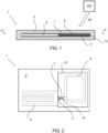
- FIG. 1 and 2 there is illustrated a device 1 according to the invention for detecting strains and transmitting detected data.
- said device comprises an electrically insulating matrix 3, in which there are embedded at least:
- strain sensor 5 and said electronic circuit 7 are electrically connected to each other, for example at corresponding contacts or pads 11, and also said electronic circuit 7 and said antenna 9 are electrically connected to each other, for example at corresponding contacts or pads 13.
- the strain sensor 5 can have the desired size and shape.
- the use of electrically conductive resins and electrically conductive inks allows high versatility, increasing the degrees of freedom in choosing the size and shape of the sensor; advantageously, the sensor can have a large size, much larger than that of strain sensors used in prior art, and its geometry can follow complex patterns.
- the electronic circuit 7 and the antenna 9 can be made according to any suitable technology within the reach of those skilled in the art.
- said electronic circuit 7 and said antenna 9 can be made on one and the same printed circuit board (PCB) 15.
- PCB printed circuit board
- said printed circuit board 15 is preferably made as a flexible printed circuit board, obtained for instance from a film of polyamide or a PEEK-type synthetic fabric, whereby the corresponding device 1 as a whole will exhibit some flexibility, which will allow it to adapt to structures having complex surfaces.
- the device 1 may further comprise one or more sensors (not illustrated) adapted to detect the environmental conditions of the environment surrounding the device itself, such as temperature and humidity.
- said additional sensors too will be electrically connected to the electronic circuit 7 by means of corresponding contacts or pads.
- the electronic circuit 7 may further comprise a memory unit allowing to store information about the device 1 and about the data detected by said device during its operation. More particularly, said memory device allows to permanently store in the sensor all the information necessary to interpret the effected detections (including the parameters for calibration of the sensor) and to identify the sensor. When a complex structure is to be monitored, requiring use of large number of devices 1, this considerably simplifies management by eliminating the need to maintain specific external documentations, which are complex to manage and potentially subject to becoming detached or lost.
- the device 1 further comprises a shielding layer 17 associated to the printed circuit board 15.
- Said shielding layer 17 is made of a ferritic material and its function will become apparent from the description of the operation of the device 1 according to the invention provided here below. As anticipated above, said device 1 can be applied to a newly built structure as well as to an already existing structure.
- the sensing part of the device consisting of the strain sensor 5 and the electronic circuit 7 connected thereto, is protected from external agents by the matrix 3.
- Said matrix 3 not only protects the strain sensor and its electronic circuit from atmospheric agents, but it also electrically isolates them, owing to the fact that it is made of an electrically insulating material.
- the antenna 9 allows to communicate wirelessly - for example through radio-frequency - with an external instrument 100.
- the instrument 100 is able to receive the transmitted data from the antenna 9.
- the device 1 must be provided with its own power supply means (batteries) for exciting the strain sensor 5 and supplying the electronic circuit 7.
- the wireless communication between the device 1 and the tool 100 takes place in both directions, as also shown in Figure 1 .
- the external instrument 100 supplies the device 1 with the energy required to excite the strain sensor 5.
- the dimensional variation undergone by the strain sensor due to the load (stress) to which it is subjected results in a corresponding variation of its electrical resistance; said electrical resistance variation is detected by the electronic circuit 7 and transmitted to the external instrument 100 through the antenna 9.
- the excitation energy can be supplied to the strain sensor 5 simultaneously with the interrogation thereof; alternatively, it is possible to provide for supplying power to the strain sensor 5 and interrogating it at different times, while equipping it at the same time with means for storing power (either wirelessly rechargeable from the outside or disposable).
- the magnetic component of the radio-frequency emission is the one of greatest importance.
- the presence of conductive materials in the structure to which the device 1 is applied (carbon, reinforced concrete, metals and so on) near the antenna 9 disturbs or cancels the communication, because of eddy currents that the radio-frequency emission generates in such materials. These eddy currents in turn generate a magnetic field symmetrical and opposite to the field of the radio-frequency emission, which is thus attenuated or canceled.
- the problem posed by eddy currents is even more serious, since not only must the radio-frequency communication from the antenna 9 to the external instrument 100 be preserved from the influence of said eddy currents in order to correspondingly preserve the accuracy of the transmitted data, but it is also necessary that the external instrument 100 transmits to said device 1 sufficient energy to properly excite the strain sensor 5 without any negative influence by said eddy currents. Hence the importance of the shielding layer 17.
- said shielding layer is made of a ferritic material.
- said ferritic material should preferably be chosen depending on the conductive materials in the structure to which the device 1 is applied, so that the shielding effect is optimized according to the specific characteristics of the magnetic field generated by the eddy currents. This is possible when the final destination of the device 1 - that is, the type of structure to which the device will be applied and the materials that compose it - is already known at the production stage.
- a "universal" device for detecting strains is desired, i.e. a device having a behaviour which is effective whatever its final destination may be.
- a further conductive layer (not shown) with known characteristics on the basis of which the choice of the ferritic material of the shielding layer 17 has been calibrated.
- This further conductive layer can be made (for example) of carbon. Since said conductive layer is closer than the conductive materials of the structure to be monitored to the shielding layer 17, the magnetic field generated in said conductive layer is much stronger than that generated in said structure. It follows that - being the ferritic material chosen on the basis of the characteristics of said conductive layer - the device 1 according to the invention is effectively shielded whatever the characteristics of the structure to which it is associated may be.
- the device includes only one strain sensor, it is also possible to use multiple strain sensors, for example two strain sensors arranged at 90° relative to each another, three strain sensors arranged at 120° relative to one another, and so on.
Landscapes
- Physics & Mathematics (AREA)
- General Physics & Mathematics (AREA)
- Engineering & Computer Science (AREA)
- Aviation & Aerospace Engineering (AREA)
- Arrangements For Transmission Of Measured Signals (AREA)
- Measurement Of Length, Angles, Or The Like Using Electric Or Magnetic Means (AREA)
Claims (9)
- Vorrichtung (1) zur Detektion von Belastungen und zur Übertragung von detektierten Daten, mit einer elektrisch isolierenden Matrix (3) in die wenigstens eingebettet sind:- einer oder mehrere Belastungssensoren (5), die als Widerstandselemente ausgebildet sind, deren Änderungen ihrer Ausdehnung Änderungen des elektrischen Widerstands mit sich bringen;- einer elektronischen Schaltung (7), die elektrisch an den oder die Sensoren an entsprechenden Kontakten oder Flächen (11) angeschlossen und dafür ausgelegt ist, die Änderungen des elektrischen Widerstands zu detektieren;- einer Antenne (9), die elektrisch an die elektronische Schaltung an entsprechenden Kontakten oder Flächen (13) angeschlossen und dafür ausgelegt ist, die von der elektrischen Schaltung detektierten Änderungen des elektrischen Widerstandes an ein externes Instrument zu übermitteln,wobei der die Belastungssensoren (5) aus einem Material hergestellt sind, das aus einer Gruppe ausgewählt ist, die elektrisch leitende Harze und elektrisch leitende Tinten enthält,dadurch gekennzeichnet, dass in die elektrisch isolierende Matrix (3) zusätzlich eine aus ferritischem Material hergestellte Abschirmschicht (17), die an die elektronische Schaltung (7) und die Antenne (9) gekoppelt ist, eingebettet ist.
- Vorrichtung (1) nach Anspruch 1, wobei der oder die Belastungssensoren (5) aus einem elektrisch leitenden Harz hergestellt sind.
- Vorrichtung (1) nach Anspruch 1, wobei der oder die Belastungssensoren (5) aus einer elektrisch leitenden Tinte hergestellt sind.
- Vorrichtung (1) nach Anspruch 1, wobei die elektronische Schaltung (7) und die Antenne (9) auf derselben Leiterplatte (15) ausgebildet sind.
- Vorrichtung (1) nach Anspruch 4, wobei die Leiterplatte (15) als eine flexible Leiterplatte ausgebildet ist.
- Vorrichtung (1) nach Anspruch 1, wobei eine weitere leitende Schicht der Abschirmschicht zugeordnet ist.
- Vorrichtung (1) nach einem der Ansprüche 1 bis 6, zusätzlich mit einem oder mehreren Sensoren in der Matrix (3), die dafür ausgelegt sind, Umgebungsbedingungen der die Vorrichtung (1) umgebenden Umgebung zu detektieren, wie beispielsweise Temperatur und Feuchtigkeit.
- Vorrichtung (1) nach einem der Ansprüche 1 bis 7, mit zwei oder mehr Belastungssensoren (5), die unter 90° relativ zueinander angeordnet sind.
- Vorrichtung (1) nach einem der Ansprüche 1 bis 7 mit drei Belastungssensoren (5) die unter 120° relativ zueinander angeordnet sind.
Applications Claiming Priority (2)
| Application Number | Priority Date | Filing Date | Title |
|---|---|---|---|
| ITTO2015U000046U ITTO20150046U1 (it) | 2015-04-10 | 2015-04-10 | Dispositivo per la rilevazione di deformazioni e la trasmissione dei dati rilevati |
| PCT/IB2016/051922 WO2016162788A1 (en) | 2015-04-10 | 2016-04-05 | Device for detecting strains and transmitting detected data |
Publications (3)
| Publication Number | Publication Date |
|---|---|
| EP3280988A1 EP3280988A1 (de) | 2018-02-14 |
| EP3280988B1 true EP3280988B1 (de) | 2025-01-22 |
| EP3280988C0 EP3280988C0 (de) | 2025-01-22 |
Family
ID=56087464
Family Applications (1)
| Application Number | Title | Priority Date | Filing Date |
|---|---|---|---|
| EP16725900.1A Active EP3280988B1 (de) | 2015-04-10 | 2016-04-05 | Vorrichtung zur detektion von belastungen und zur übertragung von detektierten daten |
Country Status (4)
| Country | Link |
|---|---|
| US (1) | US20180106691A1 (de) |
| EP (1) | EP3280988B1 (de) |
| IT (1) | ITTO20150046U1 (de) |
| WO (1) | WO2016162788A1 (de) |
Families Citing this family (4)
| Publication number | Priority date | Publication date | Assignee | Title |
|---|---|---|---|---|
| CN110333013B (zh) * | 2019-07-15 | 2021-01-08 | 承德石油高等专科学校 | 一种嵌入式应力传感器 |
| GB2588683A (en) * | 2019-11-04 | 2021-05-05 | Nokia Technologies Oy | Electromechanical sensors |
| CN112325787A (zh) * | 2020-11-02 | 2021-02-05 | 中国电子科技集团公司第十四研究所 | 一种可测量形变的天线结构设计 |
| IT202100001457A1 (it) * | 2021-01-26 | 2022-07-26 | Tikat S R L S | Dispositivo per la rilevazione di una grandezza fisica e sistema per la rilevazione di una grandezza fisica comprendente una pluralità di siffatti dispositivi |
Citations (1)
| Publication number | Priority date | Publication date | Assignee | Title |
|---|---|---|---|---|
| ITTO20120325A1 (it) * | 2012-04-13 | 2013-10-14 | Marco Bonvino | Sistema per la misurazione di sollecitazioni e parametri ambientali all'interno di materiali compositi e per la trasmissione a distanza di tali misurazioni. |
Family Cites Families (36)
| Publication number | Priority date | Publication date | Assignee | Title |
|---|---|---|---|---|
| US4744252A (en) * | 1987-05-19 | 1988-05-17 | The United States Of America As Represented By The United States Department Of Energy | Triple-material stress-strain resistivity gage |
| US4964145A (en) * | 1989-07-24 | 1990-10-16 | International Business Machines Corporation | System for magnification correction of conductive X-ray lithography mask substrates |
| US5184516A (en) * | 1991-07-31 | 1993-02-09 | Hughes Aircraft Company | Conformal circuit for structural health monitoring and assessment |
| US5328551A (en) * | 1992-10-28 | 1994-07-12 | Eaton Corporation | Method of making high output strain gage |
| DE4236985C1 (de) * | 1992-11-04 | 1994-02-24 | Hottinger Messtechnik Baldwin | Dehnungsmeßstreifen |
| US5541570A (en) * | 1994-12-09 | 1996-07-30 | Force Imaging Technologies, Inc. | Force sensing ink, method of making same and improved force sensor |
| JPH095014A (ja) * | 1995-06-19 | 1997-01-10 | Hirano Denshi:Kk | 曲げセンサ |
| AU2059597A (en) * | 1996-02-28 | 1997-09-16 | Sigma-Netics, Inc. | Improved strain gauge and method of manufacture |
| US5734110A (en) * | 1996-10-11 | 1998-03-31 | Kistler-Morse Corporation | Temperature compensated, easily installed bolt-on strain sensor |
| AU2002349058B2 (en) * | 2002-10-15 | 2009-12-24 | Verdtech Nuevo Campo, S.A. | Precision dendrometer |
| ITPV20030001A1 (it) * | 2003-01-31 | 2004-08-01 | Ferdinando Auricchio | Sensore dotato di capacita' portanti per il monitoraggio strutturale con lettura a distanza priva di collegamento diretto. |
| US7930815B2 (en) * | 2003-04-11 | 2011-04-26 | Avery Dennison Corporation | Conductive pattern and method of making |
| JP4303091B2 (ja) * | 2003-11-10 | 2009-07-29 | ニッタ株式会社 | 歪みゲージ型センサおよびこれを利用した歪みゲージ型センサユニット |
| US6948377B2 (en) * | 2003-12-08 | 2005-09-27 | Honeywell International, Inc. | Method and apparatus for detecting the strain levels imposed on a circuit board |
| US6964205B2 (en) * | 2003-12-30 | 2005-11-15 | Tekscan Incorporated | Sensor with plurality of sensor elements arranged with respect to a substrate |
| US7461560B2 (en) * | 2005-03-28 | 2008-12-09 | Microstrain, Inc. | Strain gauge with moisture barrier and self-testing circuit |
| US7430920B2 (en) * | 2005-12-16 | 2008-10-07 | Hitachi, Ltd. | Apparatus for measuring a mechanical quantity |
| US7921727B2 (en) * | 2004-06-25 | 2011-04-12 | University Of Dayton | Sensing system for monitoring the structural health of composite structures |
| DE102004036708A1 (de) * | 2004-07-29 | 2006-03-23 | Linde Ag | Verfahren zum Verflüssigen eines Kohlenwasserstoff-reichen Stromes |
| US7082844B1 (en) * | 2005-02-16 | 2006-08-01 | Cts Corporation | Strain sensor having improved accuracy |
| JP4617943B2 (ja) * | 2005-03-18 | 2011-01-26 | 株式会社日立製作所 | 力学量測定装置 |
| JP2007271285A (ja) * | 2006-03-30 | 2007-10-18 | Millenium Gate Technology Co Ltd | ひずみゲージの製造方法 |
| JP4758271B2 (ja) * | 2006-04-18 | 2011-08-24 | 株式会社共和電業 | 大ひずみ測定用ひずみゲージ |
| DE102006035274B4 (de) * | 2006-07-31 | 2008-07-03 | Technische Universität Dresden | Faserverbundbauteil mit einer Sensor- und Anzeigeeinheit |
| JP5166714B2 (ja) * | 2006-09-15 | 2013-03-21 | 東海ゴム工業株式会社 | センサー用架橋エラストマー体およびその製法 |
| US7696676B2 (en) * | 2006-12-18 | 2010-04-13 | Lockheed Martin Corporation | Piezoelectric composite apparatus and related methods |
| EP2065681A1 (de) * | 2007-11-30 | 2009-06-03 | Paramata Limited | Messsystem und Messverfahren |
| WO2010065503A2 (en) * | 2008-12-01 | 2010-06-10 | University Of Massachusetts Lowell | Conductive formulations for use in electrical, electronic and rf applications |
| FR2944865B1 (fr) * | 2009-04-27 | 2011-06-24 | Commissariat Energie Atomique | Capteur de contrainte et son procede de realisation. |
| US9038483B2 (en) * | 2009-09-08 | 2015-05-26 | University Of Massachusetts | Wireless passive radio-frequency strain and displacement sensors |
| GB201004224D0 (en) * | 2010-03-15 | 2010-04-28 | Rolls Royce Plc | A strain assembly and method |
| KR101480752B1 (ko) * | 2012-03-30 | 2015-01-09 | 한국과학기술원 | 표면 형상 측정 장치 |
| FR3007520A1 (fr) * | 2013-06-25 | 2014-12-26 | St Microelectronics Crolles 2 | Procede de determination d'un champ de contraintes tridimensionnelles d'un objet, en particulier une structure integree, et systeme correspondant |
| ITTO20130825A1 (it) * | 2013-10-11 | 2015-04-12 | Marco Bonvino | Dispositivo per la rilevazione di deformazioni e la trasmissione dei dati rilevati e metodo per la sua realizzazione |
| WO2015073944A2 (en) * | 2013-11-18 | 2015-05-21 | President And Fellows Of Harvard College | Printed stretchable strain sensor |
| US9729193B2 (en) * | 2014-11-11 | 2017-08-08 | Ut-Battelle, Llc | Wireless sensor platform |
-
2015
- 2015-04-10 IT ITTO2015U000046U patent/ITTO20150046U1/it unknown
-
2016
- 2016-04-05 WO PCT/IB2016/051922 patent/WO2016162788A1/en not_active Ceased
- 2016-04-05 US US15/564,790 patent/US20180106691A1/en not_active Abandoned
- 2016-04-05 EP EP16725900.1A patent/EP3280988B1/de active Active
Patent Citations (1)
| Publication number | Priority date | Publication date | Assignee | Title |
|---|---|---|---|---|
| ITTO20120325A1 (it) * | 2012-04-13 | 2013-10-14 | Marco Bonvino | Sistema per la misurazione di sollecitazioni e parametri ambientali all'interno di materiali compositi e per la trasmissione a distanza di tali misurazioni. |
Non-Patent Citations (1)
| Title |
|---|
| MERILAMPI SARI ET AL: "Embedded wireless strain sensors based on printed RFID tag", SENSOR REVIEW, vol. 31, no. 1, 25 January 2011 (2011-01-25), GB, pages 32 - 40, XP055932490, ISSN: 0260-2288, DOI: 10.1108/02602281111099062 * |
Also Published As
| Publication number | Publication date |
|---|---|
| EP3280988A1 (de) | 2018-02-14 |
| ITTO20150046U1 (it) | 2016-10-10 |
| EP3280988C0 (de) | 2025-01-22 |
| WO2016162788A1 (en) | 2016-10-13 |
| US20180106691A1 (en) | 2018-04-19 |
Similar Documents
| Publication | Publication Date | Title |
|---|---|---|
| US11586872B2 (en) | Metal fastener with embedded RFID tag and method of production | |
| US7276137B2 (en) | Textile product having an integrated sensor for measuring pressure and temperature | |
| US10234334B2 (en) | Sensor tag and manufacturing method for sensor tag | |
| US10948357B2 (en) | Smart parts: embedded sensors for use in additive manufactured parts | |
| US9759543B2 (en) | Device for detecting strains and transmitting detected data and method for manufacturing the same | |
| US20090145971A1 (en) | Printed wireless rf identification label structure | |
| US10031031B2 (en) | Wireless temperature sensing method using no electrical connections | |
| Bhattacharyya et al. | RFID tag antenna based temperature sensing in the frequency domain | |
| EP1145021A1 (de) | Verfahren und vorrichtung zur kontaktlosen feststellung eines äusseren elektrischen oder magnetischen felds | |
| ITMI20130482A1 (it) | Dispositivo elettronico integrato per il monitoraggio di pressione all'interno di una struttura solida | |
| US20180106691A1 (en) | Device for detecting strains and transmitting detected data | |
| Wang et al. | All-around package security using radio frequency identification threads | |
| EP4080409A1 (de) | Rohrleitung mit funkfrequenzidentifikations(rfid)-fähigem sensor | |
| US10833531B2 (en) | Electric power generation or distribution asset monitoring | |
| CN112304355B (zh) | 具有近场天线的测量装置 | |
| KR20190059156A (ko) | 응력을 측정하기 위한 센서 및 그것을 포함하는 시스템 | |
| JP2000132654A (ja) | 非接触データキャリアパッケージ | |
| US11371823B1 (en) | Magnetoelastic strain sensor and radio-frequency identification tag including the same | |
| FI128912B (fi) | Menetelmä fysikaalisten suureitten mittaamiseksi ja menetelmässä hyödynnettävä mittausjärjestely | |
| CN210375509U (zh) | 具无线射频表计结构 | |
| WO2017110788A1 (ja) | ワイヤハーネス | |
| CN104160410A (zh) | 借助rfid标记产生触发事件 | |
| JP2005221337A (ja) | トルク検出装置及びトルク較正情報作成装置 | |
| Wang et al. | Wireless Phase-Based Displacement Sensor Using Coupled RFID Tags | |
| CN102064385A (zh) | 一种融合封装超高频天线 |
Legal Events
| Date | Code | Title | Description |
|---|---|---|---|
| STAA | Information on the status of an ep patent application or granted ep patent |
Free format text: STATUS: THE INTERNATIONAL PUBLICATION HAS BEEN MADE |
|
| PUAI | Public reference made under article 153(3) epc to a published international application that has entered the european phase |
Free format text: ORIGINAL CODE: 0009012 |
|
| STAA | Information on the status of an ep patent application or granted ep patent |
Free format text: STATUS: REQUEST FOR EXAMINATION WAS MADE |
|
| 17P | Request for examination filed |
Effective date: 20171010 |
|
| AK | Designated contracting states |
Kind code of ref document: A1 Designated state(s): AL AT BE BG CH CY CZ DE DK EE ES FI FR GB GR HR HU IE IS IT LI LT LU LV MC MK MT NL NO PL PT RO RS SE SI SK SM TR |
|
| AX | Request for extension of the european patent |
Extension state: BA ME |
|
| DAV | Request for validation of the european patent (deleted) | ||
| DAX | Request for extension of the european patent (deleted) | ||
| RAP1 | Party data changed (applicant data changed or rights of an application transferred) |
Owner name: INSENSUS PROJECT S.R.L. |
|
| STAA | Information on the status of an ep patent application or granted ep patent |
Free format text: STATUS: EXAMINATION IS IN PROGRESS |
|
| 17Q | First examination report despatched |
Effective date: 20201021 |
|
| GRAP | Despatch of communication of intention to grant a patent |
Free format text: ORIGINAL CODE: EPIDOSNIGR1 |
|
| STAA | Information on the status of an ep patent application or granted ep patent |
Free format text: STATUS: GRANT OF PATENT IS INTENDED |
|
| INTG | Intention to grant announced |
Effective date: 20240906 |
|
| GRAS | Grant fee paid |
Free format text: ORIGINAL CODE: EPIDOSNIGR3 |
|
| GRAA | (expected) grant |
Free format text: ORIGINAL CODE: 0009210 |
|
| STAA | Information on the status of an ep patent application or granted ep patent |
Free format text: STATUS: THE PATENT HAS BEEN GRANTED |
|
| AK | Designated contracting states |
Kind code of ref document: B1 Designated state(s): AL AT BE BG CH CY CZ DE DK EE ES FI FR GB GR HR HU IE IS IT LI LT LU LV MC MK MT NL NO PL PT RO RS SE SI SK SM TR |
|
| REG | Reference to a national code |
Ref country code: GB Ref legal event code: FG4D |
|
| REG | Reference to a national code |
Ref country code: CH Ref legal event code: EP |
|
| REG | Reference to a national code |
Ref country code: IE Ref legal event code: FG4D |
|
| REG | Reference to a national code |
Ref country code: DE Ref legal event code: R096 Ref document number: 602016091000 Country of ref document: DE |
|
| U01 | Request for unitary effect filed |
Effective date: 20250212 |
|
| U07 | Unitary effect registered |
Designated state(s): AT BE BG DE DK EE FI FR IT LT LU LV MT NL PT RO SE SI Effective date: 20250218 |
|
| PG25 | Lapsed in a contracting state [announced via postgrant information from national office to epo] |
Ref country code: RS Free format text: LAPSE BECAUSE OF FAILURE TO SUBMIT A TRANSLATION OF THE DESCRIPTION OR TO PAY THE FEE WITHIN THE PRESCRIBED TIME-LIMIT Effective date: 20250422 |
|
| PG25 | Lapsed in a contracting state [announced via postgrant information from national office to epo] |
Ref country code: PL Free format text: LAPSE BECAUSE OF FAILURE TO SUBMIT A TRANSLATION OF THE DESCRIPTION OR TO PAY THE FEE WITHIN THE PRESCRIBED TIME-LIMIT Effective date: 20250122 |
|
| PG25 | Lapsed in a contracting state [announced via postgrant information from national office to epo] |
Ref country code: ES Free format text: LAPSE BECAUSE OF FAILURE TO SUBMIT A TRANSLATION OF THE DESCRIPTION OR TO PAY THE FEE WITHIN THE PRESCRIBED TIME-LIMIT Effective date: 20250122 |
|
| PG25 | Lapsed in a contracting state [announced via postgrant information from national office to epo] |
Ref country code: IS Free format text: LAPSE BECAUSE OF FAILURE TO SUBMIT A TRANSLATION OF THE DESCRIPTION OR TO PAY THE FEE WITHIN THE PRESCRIBED TIME-LIMIT Effective date: 20250522 Ref country code: NO Free format text: LAPSE BECAUSE OF FAILURE TO SUBMIT A TRANSLATION OF THE DESCRIPTION OR TO PAY THE FEE WITHIN THE PRESCRIBED TIME-LIMIT Effective date: 20250422 |
|
| PG25 | Lapsed in a contracting state [announced via postgrant information from national office to epo] |
Ref country code: HR Free format text: LAPSE BECAUSE OF FAILURE TO SUBMIT A TRANSLATION OF THE DESCRIPTION OR TO PAY THE FEE WITHIN THE PRESCRIBED TIME-LIMIT Effective date: 20250122 |
|
| PG25 | Lapsed in a contracting state [announced via postgrant information from national office to epo] |
Ref country code: GR Free format text: LAPSE BECAUSE OF FAILURE TO SUBMIT A TRANSLATION OF THE DESCRIPTION OR TO PAY THE FEE WITHIN THE PRESCRIBED TIME-LIMIT Effective date: 20250423 |
|
| PG25 | Lapsed in a contracting state [announced via postgrant information from national office to epo] |
Ref country code: SM Free format text: LAPSE BECAUSE OF FAILURE TO SUBMIT A TRANSLATION OF THE DESCRIPTION OR TO PAY THE FEE WITHIN THE PRESCRIBED TIME-LIMIT Effective date: 20250122 |
|
| PG25 | Lapsed in a contracting state [announced via postgrant information from national office to epo] |
Ref country code: CZ Free format text: LAPSE BECAUSE OF FAILURE TO SUBMIT A TRANSLATION OF THE DESCRIPTION OR TO PAY THE FEE WITHIN THE PRESCRIBED TIME-LIMIT Effective date: 20250122 |
|
| PG25 | Lapsed in a contracting state [announced via postgrant information from national office to epo] |
Ref country code: SK Free format text: LAPSE BECAUSE OF FAILURE TO SUBMIT A TRANSLATION OF THE DESCRIPTION OR TO PAY THE FEE WITHIN THE PRESCRIBED TIME-LIMIT Effective date: 20250122 |
|
| REG | Reference to a national code |
Ref country code: CH Ref legal event code: H13 Free format text: ST27 STATUS EVENT CODE: U-0-0-H10-H13 (AS PROVIDED BY THE NATIONAL OFFICE) Effective date: 20251125 |
|
| PLBE | No opposition filed within time limit |
Free format text: ORIGINAL CODE: 0009261 |
|
| STAA | Information on the status of an ep patent application or granted ep patent |
Free format text: STATUS: NO OPPOSITION FILED WITHIN TIME LIMIT |
|
| U21 | Renewal fee for the european patent with unitary effect paid with additional fee |
Year of fee payment: 10 Effective date: 20251027 |
|
| PG25 | Lapsed in a contracting state [announced via postgrant information from national office to epo] |
Ref country code: MC Free format text: LAPSE BECAUSE OF FAILURE TO SUBMIT A TRANSLATION OF THE DESCRIPTION OR TO PAY THE FEE WITHIN THE PRESCRIBED TIME-LIMIT Effective date: 20250122 |
|
| GBPC | Gb: european patent ceased through non-payment of renewal fee |
Effective date: 20250422 |
|
| 26N | No opposition filed |
Effective date: 20251023 |
|
| PG25 | Lapsed in a contracting state [announced via postgrant information from national office to epo] |
Ref country code: GB Free format text: LAPSE BECAUSE OF NON-PAYMENT OF DUE FEES Effective date: 20250422 |
|
| PG25 | Lapsed in a contracting state [announced via postgrant information from national office to epo] |
Ref country code: CH Free format text: LAPSE BECAUSE OF NON-PAYMENT OF DUE FEES Effective date: 20250430 |
|
| PG25 | Lapsed in a contracting state [announced via postgrant information from national office to epo] |
Ref country code: IE Free format text: LAPSE BECAUSE OF NON-PAYMENT OF DUE FEES Effective date: 20250405 |