EP3281226B1 - Substrat de commande tactile oled et son procédé de fabrication, et dispositif d'affichage - Google Patents
Substrat de commande tactile oled et son procédé de fabrication, et dispositif d'affichage Download PDFInfo
- Publication number
- EP3281226B1 EP3281226B1 EP15851612.0A EP15851612A EP3281226B1 EP 3281226 B1 EP3281226 B1 EP 3281226B1 EP 15851612 A EP15851612 A EP 15851612A EP 3281226 B1 EP3281226 B1 EP 3281226B1
- Authority
- EP
- European Patent Office
- Prior art keywords
- touch
- electrodes
- control
- oleds
- electrode lines
- Prior art date
- Legal status (The legal status is an assumption and is not a legal conclusion. Google has not performed a legal analysis and makes no representation as to the accuracy of the status listed.)
- Active
Links
Images




Classifications
-
- G—PHYSICS
- G06—COMPUTING OR CALCULATING; COUNTING
- G06F—ELECTRIC DIGITAL DATA PROCESSING
- G06F3/00—Input arrangements for transferring data to be processed into a form capable of being handled by the computer; Output arrangements for transferring data from processing unit to output unit, e.g. interface arrangements
- G06F3/01—Input arrangements or combined input and output arrangements for interaction between user and computer
- G06F3/03—Arrangements for converting the position or the displacement of a member into a coded form
- G06F3/041—Digitisers, e.g. for touch screens or touch pads, characterised by the transducing means
- G06F3/0412—Digitisers structurally integrated in a display
-
- G—PHYSICS
- G06—COMPUTING OR CALCULATING; COUNTING
- G06F—ELECTRIC DIGITAL DATA PROCESSING
- G06F3/00—Input arrangements for transferring data to be processed into a form capable of being handled by the computer; Output arrangements for transferring data from processing unit to output unit, e.g. interface arrangements
- G06F3/01—Input arrangements or combined input and output arrangements for interaction between user and computer
- G06F3/03—Arrangements for converting the position or the displacement of a member into a coded form
- G06F3/041—Digitisers, e.g. for touch screens or touch pads, characterised by the transducing means
- G06F3/044—Digitisers, e.g. for touch screens or touch pads, characterised by the transducing means by capacitive means
- G06F3/0445—Digitisers, e.g. for touch screens or touch pads, characterised by the transducing means by capacitive means using two or more layers of sensing electrodes, e.g. using two layers of electrodes separated by a dielectric layer
-
- G—PHYSICS
- G06—COMPUTING OR CALCULATING; COUNTING
- G06F—ELECTRIC DIGITAL DATA PROCESSING
- G06F3/00—Input arrangements for transferring data to be processed into a form capable of being handled by the computer; Output arrangements for transferring data from processing unit to output unit, e.g. interface arrangements
- G06F3/01—Input arrangements or combined input and output arrangements for interaction between user and computer
- G06F3/03—Arrangements for converting the position or the displacement of a member into a coded form
- G06F3/041—Digitisers, e.g. for touch screens or touch pads, characterised by the transducing means
- G06F3/044—Digitisers, e.g. for touch screens or touch pads, characterised by the transducing means by capacitive means
- G06F3/0446—Digitisers, e.g. for touch screens or touch pads, characterised by the transducing means by capacitive means using a grid-like structure of electrodes in at least two directions, e.g. using row and column electrodes
-
- H—ELECTRICITY
- H10—SEMICONDUCTOR DEVICES; ELECTRIC SOLID-STATE DEVICES NOT OTHERWISE PROVIDED FOR
- H10K—ORGANIC ELECTRIC SOLID-STATE DEVICES
- H10K59/00—Integrated devices, or assemblies of multiple devices, comprising at least one organic light-emitting element covered by group H10K50/00
- H10K59/10—OLED displays
- H10K59/12—Active-matrix OLED [AMOLED] displays
- H10K59/131—Interconnections, e.g. wiring lines or terminals
-
- H—ELECTRICITY
- H10—SEMICONDUCTOR DEVICES; ELECTRIC SOLID-STATE DEVICES NOT OTHERWISE PROVIDED FOR
- H10K—ORGANIC ELECTRIC SOLID-STATE DEVICES
- H10K59/00—Integrated devices, or assemblies of multiple devices, comprising at least one organic light-emitting element covered by group H10K50/00
- H10K59/10—OLED displays
- H10K59/17—Passive-matrix OLED displays
- H10K59/179—Interconnections, e.g. wiring lines or terminals
-
- H—ELECTRICITY
- H10—SEMICONDUCTOR DEVICES; ELECTRIC SOLID-STATE DEVICES NOT OTHERWISE PROVIDED FOR
- H10K—ORGANIC ELECTRIC SOLID-STATE DEVICES
- H10K59/00—Integrated devices, or assemblies of multiple devices, comprising at least one organic light-emitting element covered by group H10K50/00
- H10K59/40—OLEDs integrated with touch screens
-
- H—ELECTRICITY
- H10—SEMICONDUCTOR DEVICES; ELECTRIC SOLID-STATE DEVICES NOT OTHERWISE PROVIDED FOR
- H10K—ORGANIC ELECTRIC SOLID-STATE DEVICES
- H10K71/00—Manufacture or treatment specially adapted for the organic devices covered by this subclass
-
- H—ELECTRICITY
- H10—SEMICONDUCTOR DEVICES; ELECTRIC SOLID-STATE DEVICES NOT OTHERWISE PROVIDED FOR
- H10K—ORGANIC ELECTRIC SOLID-STATE DEVICES
- H10K71/00—Manufacture or treatment specially adapted for the organic devices covered by this subclass
- H10K71/60—Forming conductive regions or layers, e.g. electrodes
-
- G—PHYSICS
- G06—COMPUTING OR CALCULATING; COUNTING
- G06F—ELECTRIC DIGITAL DATA PROCESSING
- G06F2203/00—Indexing scheme relating to G06F3/00 - G06F3/048
- G06F2203/041—Indexing scheme relating to G06F3/041 - G06F3/045
- G06F2203/04103—Manufacturing, i.e. details related to manufacturing processes specially suited for touch sensitive devices
-
- H—ELECTRICITY
- H10—SEMICONDUCTOR DEVICES; ELECTRIC SOLID-STATE DEVICES NOT OTHERWISE PROVIDED FOR
- H10K—ORGANIC ELECTRIC SOLID-STATE DEVICES
- H10K71/00—Manufacture or treatment specially adapted for the organic devices covered by this subclass
- H10K71/20—Changing the shape of the active layer in the devices, e.g. patterning
Definitions
- the present invention generally relates to the field of the display technologies and, more particularly, to an OLED touch-control substrate and fabrication methods thereof, and a display apparatus.
- OLED Organic Light-Emitting Diode
- the basic structure of an OLED includes an anode, a cathode, and a light-emitting layer between the anode and the cathode.
- Light-emitting of OLED is caused by the injection and combination of carriers through the anode and the cathode when an external electric field is applied on the light-emitting layer.
- the carriers e.g., holes and electrons
- the carriers are transported between the anode to the cathode under the electric field; and combined into exitons when the holes and the electrons meet within the light-emitting layer.
- the exitons release energy to activate the light-emitting molecules.
- the activated light-emitting molecules emit visible light by a radiation relaxation process.
- OLED touch-control substrates usually formed by a plug-in architecture. That is, a touch-control screen and an OLED display are fabricated separately, and then bonded together.
- Such a technology has many disadvantages, such as large module thickness, low light transparency and high production cost, etc.
- the disclosed device structures, methods and systems are directed to at least partially solve one or more problems set forth above and other problems.
- Chinese utility model CN 204204861 U discloses an array substrate, a touch control display panel, and a touch control display device, so as to achieve the application of In-cell touch control technology of an AMOLED display under different technologies.
- the array substrate comprises a substrate, and the substrate is provided with a plurality of pixel units which are formed by the enclosing of data lines and grid lines, wherein the data lines and the grid lines are intersected with each other.
- Each pixel unit comprises an OLED display device of a bottom emission type and at least one TFT, wherein the OLED display device comprises a transparent anode.
- the array substrate also comprises a plurality of first electrodes which are parallel to the data lines and are arranged on the same layer as the data lines.
- the array substrate also comprises a plurality of second electrodes which are parallel to the data lines and are arranged on the same layer as the anode of the grid lines. At least one first electrode forms a touch control drive line, and at least one second electrode forms a touch control induction line.
- Chinese patent application CN 104409467 A discloses a touch panel and manufacturing method thereof and a display device, wherein the touch panel comprises: a first substrate and a second substrate oppositely disposed; an organic light emitting layer located between the first substrate and the second substrate, wherein the organic light emitting layer includes at least a cathode layer formed by a plurality of strip-like cathode electrodes; and a first touch layer located between the first substrate and the second substrate, wherein the first touch layer comprises a plurality of first touch electrodes, the first touch electrode comprises at least one first touch sub electrode the projection on the organic light emitting layer of which is located between two adjacent cathode electrodes.
- the technical solution of the invention can reduce at least electromagnetic interference between the first touch layer and the cathode electrode, and thus can improve the touch effect and the display effect.
- the invention can further reduce manufacture procedure of the process and reduce product costs.
- European patent application EP 1811571 A2 discloses an organic light emitting display and a method of fabricating the same that are capable of preventing an element from being damaged due to a large amount of heat generated when the laser irradiates a glass frit for sealing a substrate.
- the organic light emitting display includes: a first substrate (300) comprising a pixel region (I) and a non-pixel region (II); an array of organic light emitting pixels formed over the pixel region; a conductive line (360d) formed over the non-pixel region; a second substrate (420) placed over the first substrate such that the array and the conductive line are interposed between the first and second substrates; and a frit seal interposed between the first and second substrates and surrounding the array, the frit seal (430) interconnecting the first and second substrates, the frit seal comprising a portion overlapping the conductive line, wherein when viewed from the second substrate, the portion of the frit seal substantially eclipses the conductive line.
- the organic light-emitting diode (OLED) touch-control substrate comprises a plurality of OLEDs, each of the OLEDs having a first electrode, a second electrode and a light-emitting layer between the first electrode and the second electrode; a plurality of first touch-control electrodes disposed in a same layer with first electrodes of the OLEDs and insulated from the first electrodes; a plurality of second touch-control electrodes disposed in a same layer with second electrodes of the OLEDs and insulated from the second electrodes and the first touch-control electrodes; and a first insulation layer disposed between the layer having the first touch-control electrodes and the first electrodes and the layer having the second touch-control electrodes and the second electrodes, having via holes at positions corresponding to light-emitting layers of the OLEDs, the light-emitting layers being in the via holes.
- the first touch-control electrodes and the second touch-control electrodes configured for realizing a touch-control function are embedded in the OLED touch-control substrate.
- the thickness of the modules of the OLED touch-control substrate may be significantly reduced; the light transmittance may be increased; and the production cost may be reduced.
- the organic light-emitting diode (OLED) touch-control substrate further includes a plurality of insulation blocks disposed at cross-positions of the first touch-control electrodes.
- one first touch-control electrode is disposed between at least two adjacent first electrode lines; and one second touch-control electrode is disposed between at least two adjacent second electrode lines
- the OLEDs comprises passive matrix OLEDs (PMOLEDs) having a plurality of first electrode lines and second electrode lines, the first electrode lines electrically connecting the first electrodes, the second electrode lines connecting the second electrodes; the plurality of first touch-control electrodes are parallel to the plurality of first electrode lines and insulated from the plurality of the first electrode lines; and the plurality of second touch-control electrodes are parallel to the plurality of second electrode lines and insulated from the second electrode lines.
- PMOLEDs passive matrix OLEDs
- the OLEDs comprises active matrix OLEDs (AMOLEDs); the plurality of first touch-control electrodes are electrically insulated from the plurality of first electrodes of the AMOLEDs; and a plurality of second electrode of the AMOLEDs are electrically connected.
- AMOLEDs active matrix OLEDs
- the organic light-emitting diode (OLED) touch-control substrate further includes thin film transistors for controlling the plurality of OLEDs.
- the organic light-emitting diode (OLED) touch-control substrate further includes gate lines connecting to gates of thin film transistors; and data lines connecting to sources of the thin film transistors.
- the first touch-control electrodes are parallel to one of the gate lines and the data lines; and the second touch-control electrodes are parallel to the other one of the gate lines and the data lines.
- the first electrodes are one of the anodes and the cathode; and the second electrodes are the other one of the anodes and the cathodes.
- the first touch-control electrodes are one of the driving electrode lines and sensing electrode lines; and the second touch-control electrodes are the other one of the driving electrodes and sensing electrodes.
- Another aspect of the present invention is providing a method for fabricating an OLED touch-control substrate.
- the method comprises forming a plurality of first touch-control electrodes and a plurality of first electrodes of OLEDs insulated from the plurality of first touch-control electrodes in a same layer on a substrate; forming a first insulation material layer on the plurality of first touch-control electrodes and the plurality of first electrodes; forming a plurality of via holes at positions of the first insulation material layer corresponding to light-emitting layers of the OLEDs; forming the light-emitting layers in the via holes; and forming a plurality of second touch-control electrodes and a plurality of second electrodes of the OLEDs insulated from the second touch-control electrodes in a same layer on the light-emitting layers.
- the thicknesses of the modules of the OLED touch-control substrate fabricated by the disclosed method may be relatively small; and the light transmittance may be relatively large. Further, comparing with existing methods, the production cost may be relatively low.
- the method further includes forming a plurality of insulation blocks at cross positions of the first touch-control electrodes and the second touch-control electrodes.
- the OLEDs are passive matrix OLEDs (PMOLEDs) having a plurality of first electrode lines and second electrode lines; the plurality of first touch-control electrodes are parallel to the plurality of first electrode lines and insulated from the first electrode lines; and the plurality of second touch-control electrodes are parallel to the plurality of second electrode lines and insulated from the second electrode lines.
- PMOLEDs passive matrix OLEDs
- the OLEDs comprises active matrix OLEDs (AMOLEDs; the plurality of first touch-control electrodes are electrically insulated from the plurality of first electrodes; and the plurality of second electrodes are electrically connected.
- AMOLEDs active matrix OLEDs
- the plurality of first touch-control electrodes are electrically insulated from the plurality of first electrodes
- the plurality of second electrodes are electrically connected.
- the method further includes forming a plurality of thin-film transistors for controlling the plurality of OLEDs on the substrate; and forming a second insulation layer having a plurality of openings corresponding to drains of thin-film transistors connecting the drains with the first electrodes.
- the first electrodes are one of the anodes and the cathodes; and the second electrodes are the other one of the anodes and the cathodes
- the first touch-control electrodes are one of the driving electrodes and the sensing electrode; and the second touch-control electrodes are the other one of the anodes and the sensing electrodes.
- Another aspect of the present invention includes providing a display apparatus.
- the display apparatus comprises at least the disclosed OLED touch-control substrate.
- an OLED touch-control substrate and a fabrication process thereof are provided in the present disclosure.
- OLEDs can be categorized as Passive Matrix OLEDs (PMOLEDs) and Active Matrix OLED (AMOLEDs).
- PMOLEDs Passive Matrix OLEDs
- AMOLEDs Active Matrix OLED
- the anodes and cathodes form a matrix, and pixels in the matrix are turned on/off by a scanning mode. Each pixel is operated under a short pulse mode; and the emission of light in the PMOLEDs is a transient process with a relatively high light intensity.
- Figure 1 illustrates the top view of an exemplary PMOLED touch-control substrate according to the disclosed embodiments.
- the PMOLED touch-control substrate may include a plurality of OLEDs (not labeled).
- the plurality of OLEDs may be distributed as an array, i.e., a plurality of rows and a plurality of columns.
- Each of the plurality of OLEDs may include a first electrode 11, a second electrode 12, and a light-emitting layer 13 between the first electrode 11 and the second electrode 12.
- the PMOLED touch-control substrate may also include a plurality of first touch-control electrodes 14.
- the plurality of touch-control electrodes 14 may be disposed on a same layer with the first electrodes 11.
- the PMOLED touch-control substrate may also include a plurality of second touch-control electrodes 15.
- the plurality of the second touch-control electrodes 15 may be disposed on a same layer with the second electrodes 12.
- Each row or column of first electrode 11 may be electrically connected by a first electrode line 18; and each row or column of the second electrodes 12 may be electrically connected by a second electrode line 19.
- the first touch-control electrodes 14 and the second touch-control electrodes 15 may be electrically insulated by any appropriate structures.
- the PMOLED may include a first insulation layer 16 between the layer having the first electrodes 11 and the first touch-control electrodes 14 and the layer having the second electrodes 12 and the second touch-control electrodes 15; and the first insulation 16 may be used to electrically insulate the first touch-control electrodes 14 and the second touch-control electrodes 15.
- the portions of the first insulation layer 16 corresponding to the light-emitting layers 13 may have via holes (not labeled in Figure 1 ). That is, the light-emitting layers 13 may be in the via holes of the first insulation layer 16.
- insulation blocks may be formed between portions of the first touch-control electrodes 14 and the portions of the second touch-control electrodes 15 at the cross positions of the first touch-control electrodes 14 and the second touch-control electrodes 15.
- the first touch-control electrodes 14 and the second touch-control electrodes 15 may be electrically insulated.
- the OLEDs may be top-emitting OLEDs, or bottom-emitting OLEDs.
- the OLEDs may include red OLEDs, green OLEDs, or white OLEDs, etc.
- PMOLED display may also include transport layer and shared layers, etc.
- the first electrodes 11 may be anodes and the second electrodes 12 may be cathodes. In certain other embodiments, the first electrodes 11 may be cathodes and the second electrodes 12 may be anodes.
- the first electrodes 11 may be close to the substrate.
- the second electrodes 12 may be close to the substrate.
- the first touch-control electrodes 14 may be driving electrode lines, and the second touch-control electrodes 15 may be sensing electrode lines.
- the first touch-control electrodes 14 may be touch-control sensing electrode lines and the second touch-control electrodes 15 may be driving electrode lines.
- the first touch-control electrodes 14 may be close to the substrate.
- the second touch-control electrodes 15 may be close to the substrate.
- the PMOLED may also include a plurality of first electrode lines 18, and a plurality of second electrode lines 19.
- One first electrode line 18 may electrically connect one row, or one column of first electrodes 11; and one second electrode line 19 may electrically connect one row or one column of second electrodes 12.
- the plurality of first touch-control electrodes 14 may be parallel to the plurality of first electrode lines 18; and the plurality of second touch-control electrodes 15 may be parallel to the plurality of second electrode lines 19.
- the number of first electrode lines 18 and the second electrode lines 19 corresponding to one OLED may be any appropriate value.
- the light-emitting layer 13 of one OLED may be disposed at the cross-position of a first electrode line 18 and a second electrode line 19, as shown in Figure 1 .
- the line density of the first touch-control electrodes 14 and the second touch-control electrodes 15 may be any appropriate value.
- one first touch-control electrode line14 may be disposed between two adjacent first electrode lines 18, or one first touch-control electrode line 14 may be disposed between two sets of first electrode lines 18; and each set of first electrode lines 18 may include a plurality of first electrode lines 18.
- one second touch-control electrode line 15 may be disposed between two adjacent second electrode lines 19, or one second touch-control electrode line 15 may be disposed between two sets of second electrode lines 19; and each set of second electrode lines 19 may include a plurality of second electrode lines 19.
- FIG. 2 illustrates the top view of an exemplary AMOLED touch-control substrate according to the disclosed embodiments.
- the AMOLED touch-control substrate may include a plurality of OLEDs (not labeled).
- the plurality of OLEDs may be distributed as an array, i.e., a plurality of rows and a plurality of columns.
- Each of the plurality of OLEDs may include a first electrode 11, a second electrode 12, and a light-emitting layer 13 between the first electrode 11 and the second electrode 12.
- the AMOLED touch-control substrate may also include a plurality of first touch-control electrodes 14.
- the plurality of touch-control electrodes 14 may be disposed on a same layer with the first electrodes 11.
- the AMOLED touch-control substrate may also include a plurality of second touch-control electrodes 15.
- the plurality of second touch-control electrodes 15 may be disposed on a same layer with the second electrodes 12.
- the first touch-control electrodes 14 and the second touch-control electrodes 15 may be electrically insulated by any appropriate structures.
- the AMOLED touch-control substrate may include a first insulation layer 16 between the layer having the first electrodes 11 and the first touch-control electrodes 14 and the layer having the second electrodes 12 and the second touch-control electrodes 15; and the first insulation layer 16 may be used to electrically insulate the first touch-control electrodes 14 and the second touch-control electrodes 15.
- the portions of the first insulation layer 16 corresponding to the light-emitting layers 13 may have via holes (not labeled in Figure 2 ). That is, the light-emitting layers 13 may be in the via holes of the first insulation layer 16.
- insulation blocks may be formed between portions of the first touch-control electrodes 14 and the portions of the second touch-control electrodes 15 at the cross-positions of the first touch-control electrodes 14 and the second touch-control electrodes 15.
- the first touch-control electrodes 14 and the second touch-control electrodes 15 may be electrically insulated.
- the OLEDs may be top-emitting OLEDs, or bottom-emitting OLEDs.
- the OLEDs may include red OLEDs, green OLEDs, or white OLEDs, etc.
- an AMOLED display may also include transport layers and shared layers, etc.
- the first electrodes 11 may be anodes and the second electrodes 12 may be cathodes. In certain other embodiments, the first electrodes 11 may be cathodes and the second electrodes 12 may be anodes.
- the first electrodes 11 may be close to the substrate.
- the second electrodes 12 may be close to the substrate.
- the first touch-control electrodes 14 may be driving electrode lines, and the second touch-control electrodes 15 may be touch-sensing electrode lines.
- the first touch-control electrodes 14 may be touch-sensing electrode lines and the second touch-control electrodes 15 may driving electrode lines.
- the first touch-control electrodes 14 may be close to a substrate.
- the second touch-control electrodes 15 may be close to a substrate.
- the first electrodes 11 of the plurality of OLEDs may be insulated from each other; and the second electrodes 12 of the plurality of second electrodes 12 may be electrically connected.
- the AMOLED touch-control substrate may include TFTs 20 for controlling the corresponding OLEDs.
- the drain (not labeled) of the TFTs 20 may electrically connect with the first electrodes 11.
- the OLEDs may be turned on or off by controlling the TFTs 20.
- the AMOLED touch-control substrate may also include gate lines 22 and data lines 23.
- the sources of TFTs 20 may electrically connect with the data lines 23; and the gates of the TFTs 20 may electrically connect with the gate lines 23.
- the first touch-control electrodes 14 may be parallel to the data lines 23; and the second touch-control electrodes 15 may be parallel to the gate lines 22. In certain other embodiments, the first touch-control electrodes 14 may be parallel to the gate lines 22; and the second touch-control electrodes 15 may be parallel to the data lines 23.
- the first touch-control electrodes 14 and the second touch-control electrodes 15 configured to realize a touch-control function may be embedded in the OLED display. Comparing with the existing technologies, the thickness of the modules of the OLED touch-control substrate may be significantly reduced, the light transmittance may be increased; and the production cost may be reduced.
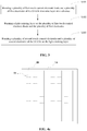
- Figure 3 illustrates an exemplary fabrication process of an OLED touch-control substrate.
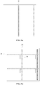
- Figures 4a ⁇ 4c illustrate structures corresponding certain stages of the exemplary fabrication for forming a PMOLED touch-control substrate.
- a plurality of first touch-control electrodes and a plurality of first electrodes of the PMOLEDs may be formed on a substrate (S101).
- Figure 4a illustrates a corresponding structure.
- a substrate (not labeled) is provided; and a plurality of first touch-control electrodes 14 and a plurality of first electrode lines 18 may be formed.
- the plurality of first touch-control electrodes 14 may be parallel to each other; and the plurality of first electrode lines 18 may be parallel to each other.
- the dashed areas on the first electrode lines 18 may be corresponding to the first electrodes 11 of the PMOLEDs. That is, the dashed areas of the first electrode lines 18 may be configured as the first electrodes 11 of the PMOLEDs, i.e., one light-emitting layer 13 may be subsequently formed on each of the dashed regions of the first electrode lines 18.
- one first electrode line 18 may be used to electrically connect one row of first electrodes 11, or one column of first electrodes 11. Further, the plurality of first touch-control electrodes 14 and the plurality of first electrode lines 18 may be on a same layer, i.e., a surface of the substrate.
- the plurality of first touch-control electrodes 14 and the plurality of first electrode lines 18 may be formed by a patterning process.
- the plurality of first touch-control electrodes 14 and the plurality of first electrode lines 18 may be formed by forming a metal layer on the surface of the substrate; and followed by patterning the metal layer.
- the plurality of first touch-control electrodes 14 and the plurality of first electrode lines 18 may be formed by a lift-off process.
- a first insulation layer may be formed.
- Figure 4b illustrates a corresponding structure.
- a first insulation layer 16 may be formed on the plurality of first touch-control electrodes 14 and the plurality of first electrode lines 18.
- the first insulation layer 16 may have a plurality of via holes 17.
- the portions of the first electrode lines 18 exposed by the via holes 17 may be configured as the first electrodes 11 of the PMOLEDs.
- the via holes 17 may be used to subsequently form a light-emitting layer.
- the light-emitting layer may be formed on the first electrodes 11.
- the first insulation layer 16 may be formed by a patterning process. Specifically, an insulation material layer may be formed on the plurality of first touch-control electrodes 14, the plurality of first electrode lines 18 and the substrate; and followed by etching the insulation material layer to expose the portion of the first electrode lines 18 corresponding to the first electrodes 11.
- a light-emitting layer may be formed (S102).
- Figure 4c illustrates a corresponding structure.
- a light-emitting layer 13 is formed in each of the via holes 17. That is, a light-emitting layer 13 is formed on each of the first electrodes 11.
- the light-emitting layer 13 may be formed by a patterning process. Specifically, a light-emitting material layer may be formed in the via holes 17 and on the first insulation layer 16; and followed by removing the portion of the light-emitting material layer on the first insulation layer 16. Thus, a light-emitting layer 13 is formed in each of the via holes 17, or on each of the first electrodes 11.
- a plurality of second touch-control electrodes and a plurality of second electrode lines may be formed (S103).
- a corresponding structure may refer to Figure 1 .
- a plurality of second touch-control electrodes 15 and a plurality of second electrodes lines 19 are formed on the first insulation layer 16 and the light-emitting layer 13.
- the plurality of second touch-control electrodes 15 and the plurality of second electrodes lines 19 may be on a same layer.
- the plurality of second touch-control electrodes 15 and the plurality of second electrode lines 19 may be parallel to each other. Further, the portions of the second electrode lines 19 contacting with the light-emitting layer 13 may be referred as second electrodes 12.
- the plurality of second touch-control electrodes 15 and the plurality of second electrodes lines 19 may be formed by a patterning process. Specifically, a second material layer may be formed on the light-emitting layer 13 and the first insulation layer 16; and followed by patterning the second material layer to form the plurality of second touch-control electrodes 15 and the plurality of second electrodes lines 19. In certain other embodiments, the plurality of second touch-control electrodes 15 and the plurality of second electrodes lines 19 may be formed by a lift-off process.
- Figures 5a ⁇ 5f illustrate structures corresponding to certain stages of the exemplary fabrication process illustrated in Figure 3 for forming an AMOLED touch-control substrate according to the disclosed embodiments.
- an AMOLED touch-control substrate may include TFTs 20, data lines 23, and gate lines 22. Further, the first electrodes 11 of the plurality of AMOLEDs may be electrically insulated; and the second electrodes 12 of the plurality of the AMOLEDs may be electrically connected.
- a plurality of TFTs 20 may be formed on a substrate; and a second insulation layer may be formed on the TFTs. The portions of the second insulation layer corresponding to the drains of the TFTs 20 may have a plurality of corresponding via holes.
- a plurality of gate lines 22 may be formed on a substrate.
- Figure 5a illustrates a corresponding structure.
- the plurality of gate lines 22 may be parallel to each other.
- the plurality of gate lines 22 may be formed by a patterning process.
- a gate dielectric layer (not shown) may be formed on the gate lines 22.
- the gate dielectric layer may be formed by any appropriate process; and may be patterned to be configured as the gate dielectric layer of the plurality of OLEDs.
- an active layer (not shown) may be formed on the gate dielectric layer.
- the active layer may be formed by any appropriate processes; and may be patterned to be configured as an active layer of the plurality of OLEDs.
- a plurality of data lines 23 may be formed on the active layer.
- TFTs 20 may be formed.
- Figure 5b illustrates the schematic of the TFTs 20.
- a second insulation layer 21 may be formed on the data lines 23 and the TFTs 20.
- the positions of the second insulation layer 21 corresponding to the drains of the TFTs 20 may have a plurality of via holes (not shown).
- a plurality of first touch-control electrodes 14 and first electrodes 11 of the plurality of OLEDs may be formed on the substrate.
- the first electrodes 11 of the plurality of OLEDs may be separated.
- the plurality of first touch-control electrodes 14 and the plurality of first electrodes 11 may be on a same layer.
- the plurality of first touch-control electrodes 14 and the first electrodes 11 of the plurality of the OLEDs may be formed by a patterning process. Specifically, a first material layer may be formed on the second insulation layer 21; and followed by patterning the first material layer. Thus, the plurality of first touch-control electrodes 14 and the first electrodes 11 of the plurality of OLEDs may be formed. In certain other embodiments, the plurality of first touch-control electrodes 14 and the first electrodes 11 of the plurality of OLEDs may be formed by a lift-off process.
- a first insulation layer 16 may be formed on the plurality of first touch-control electrodes 14 and the first electrodes 11 of the plurality of OLEDs.
- the positions of the first insulation layer 16 corresponding to the subsequently formed light-emitting layer of OLEDs may have a plurality of via holes 17. That is, the first electrodes 11 may be exposed.
- the first insulation layer 16 having the plurality of via holes 17 may be formed by a patterning process. Specifically, a first insulation material layer may be formed on the plurality of first touch-control electrodes 14, the first electrodes 11 of the plurality of OLEDs and the second insulation layer 23; and followed by etching the first insulation material layer to form the plurality of via holes 17.
- a light-emitting layer 13 is formed in each of the via holes 17. That is, the first light-emitting layer 13 is formed on the first electrodes 11.
- the light-emitting layer 13 may be formed by a patterning process. Specifically, a light-emitting material layer may be formed on the first electrodes 11 and a portion of the first insulation layer 16; and followed by removing the portion of the light-emitting material layer on the first insulation layer 16. Thus, the light-emitting layer 13 may be formed on each of the first electrodes 11.
- a plurality of second touch-control electrodes 15 and second electrodes 12 of the plurality of OLEDs may be formed on the first insulation layer 16 and the light-emitting layer 13.
- a corresponding structure is illustrated in Figure 2 .
- the plurality of second electrodes 12 of the OLEDs may be electrically connected.
- the plurality of second touch-control electrodes 15 and the second electrodes 12 may be formed on a same layer.
- the plurality of second touch-control electrodes 15 and the second electrodes 12 of the plurality of OLEDs may be formed by a patterning process. Specifically, a second material layer may be formed on the first insulation layer 16 and the light-emitting layer 13 and followed by patterning the second material. Thus, the plurality of second touch-control electrodes 15 and the second electrodes 12 of the plurality of OLEDs may be formed. In certain other embodiments, the plurality of second touch-control electrodes 15 and the second electrodes 12 of the plurality of OLEDs may be formed by a lift-off process.
- the TFTs 20 may be bottom-gated TFTs. In certain other embodiments, the TFTs 20 may be top-gated TFTs. The TFTs 20 may be used to control the light-emitting of the OLEDs.
- the module thickness of the OLED touch-control substrate formed by the disclosed methods may be relatively small, and the light transmittance may be relatively high. Further, because the first touch-control electrodes and the first electrodes of the OLEDs may be made of a same material; and the second touch-control electrodes and the second electrode may be made of a same material, it may not need extra masks and patterning processes. Thus, the production cost may be relatively low.
- a display apparatus is provided.
- Figure 6 illustrates an exemplary display apparatus 400 incorporating at least a disclosed OLED touch-control substrate and other aspects of the present disclosure.
- the display device 400 may be any appropriate device, panel or component with certain display function, such as an OLED panel, an OLED TV, an OLED monitor, an OLED cell phone, an OLED navigation system, or e-paper, etc.
- the display apparatus 400 includes a controller 402, a driver circuit 404, a memory 406, peripherals 408, and an OLED touch-control substrate 410. Certain devices may be omitted and other devices may be included.
- the controller 402 may include any appropriate processor or processors. Further, the controller 402 can include multiple cores for multi-thread or parallel processing.
- the memory 406 may include any appropriate memory modules. The memory 406 may store computer programs for implementing various processes, when executed by the controller 402.
- Peripherals 408 may include any interface devices for providing various signal interfaces. Further, peripherals 408 may include any input and output (I/O) devices. Peripherals 408 may also include any appropriate communication module for establishing connections through wired or wireless communication networks.
- the driver circuitry 404 may include any appropriate driving circuits to drive the OLED touch-control substrate 410.
- the OLED touch-control substrate 410 may be provided with image signals by the controller 402 and the driver circuit 404 for display. Because the module thickness of the disclosed OLED touch-control substrate be relatively small, the light-transmittance may be relative high; and the production cost may be reduced, the display apparatus having such a OLED touch-control substrate may also have similar advantages.
Landscapes
- Engineering & Computer Science (AREA)
- General Engineering & Computer Science (AREA)
- Theoretical Computer Science (AREA)
- Human Computer Interaction (AREA)
- Physics & Mathematics (AREA)
- General Physics & Mathematics (AREA)
- Manufacturing & Machinery (AREA)
- Microelectronics & Electronic Packaging (AREA)
- Electroluminescent Light Sources (AREA)
- Devices For Indicating Variable Information By Combining Individual Elements (AREA)
- Control Of El Displays (AREA)
Claims (14)
- Substrat de commande tactile de diodes électroluminescentes organiques (OLED), comprenant :une pluralité d'OLED, chacune des OLED ayant une première électrode (11), une seconde électrode (12) et une couche d'émission de lumière (13) entre la première électrode (11) et la seconde électrode (12) ;une pluralité de premières électrodes de commande tactile (14) disposées dans une même couche avec des premières électrodes (11) des OLED et isolées par rapport aux premières électrodes (11) ;une pluralité de secondes électrodes de commande tactile (15) disposées dans une même couche avec des secondes électrodes (12) des OLED et isolées par rapport aux secondes électrodes (12) et aux premières électrodes de commande tactile (14) ; etune première couche d'isolation (16) disposée entre la couche ayant les premières électrodes de commande tactile (14) et les premières électrodes (11) et la couche ayant les secondes électrodes de commande tactile (15) et les secondes électrodes (12), ayant des trous d'interconnexion (17) au niveau de positions correspondant à des couches d'émission de lumière (13) des OLED, les couches d'émission de lumière (13) étant dans les trous d'interconnexion (17).
- Substrat de commande tactile de diodes électroluminescentes organiques (OLED) selon la revendication 1, comprenant en outre :
une pluralité de blocs d'isolation disposés au niveau de positions de croisement des premières électrodes de commande tactile (14) et des secondes électrodes de commande tactile (15). - Substrat de commande tactile de diodes électroluminescentes organiques (OLED) selon la revendication 1 ou 2, dans lequel :les OLED comprennent des OLED à matrice passive (PMOLED) ayant une pluralité de premières lignes d'électrode (18) et de secondes lignes d'électrode (19), les premières lignes d'électrode (18) connectant électriquement les premières électrodes (11), et les secondes lignes d'électrode (19) connectant électriquement les secondes électrodes (12) ;les premières électrodes de commande tactile (14) sont parallèles à la pluralité de premières lignes d'électrode (18) et isolées par rapport à la pluralité de premières lignes d'électrode (18) ; etles secondes électrodes de commande tactile (15) sont parallèles à la pluralité de secondes lignes d'électrode (19) et isolées par rapport aux secondes lignes d'électrode (19).
- Substrat de commande tactile de diodes électroluminescentes organiques (OLED) selon la revendication 3, dans lequel :une première électrode de commande tactile (14) est disposée entre au moins deux premières lignes d'électrode (18) adjacentes ; etune seconde électrode de commande tactile (15) est disposée entre au moins deux secondes lignes d'électrode (19) adjacentes.
- Substrat de commande tactile de diodes électroluminescentes organiques (OLED) selon l'une quelconque des revendications 1 à 3, dans lequel :les OLED comprennent des OLED à matrice active (AMOLED) ;les premières électrodes de commande tactile (14) sont isolées électriquement par rapport aux premières électrodes (11) des AMOLED ; etles secondes électrodes (12) des AMOLED sont connectées électriquement.
- Substrat de commande tactile de diodes électroluminescentes organiques (OLED) selon la revendication 5, comprenant en outre :une pluralité de transistors à couche mince (20) pour commander la pluralité d'OLED ; de préférence comprenant en outre :des lignes de grille (22) se connectant à des grilles des transistors à couche mince (20) ; etdes lignes de données (23) se connectant à des sources des transistors à couche mince (20) ;de préférence, les premières électrodes de commande tactile (14) sont parallèles à une des lignes de grille (22) et des lignes de données (23) ; etles secondes électrodes de commande tactile (15) sont parallèles à l'autre des lignes de grille (22) et des lignes de données (23).
- Substrat de commande tactile de diodes électroluminescentes organiques (OLED) selon l'une quelconque des revendications 1 à 6, dans lequel :les premières électrodes (11) sont une parmi des anodes et des cathodes ; etles secondes électrodes (12) sont l'autre parmi des anodes et des cathodes ;de préférence, les premières électrodes de commande tactile (14) sont des lignes d'électrode d'attaque ; etles secondes électrodes de commande tactile (15) sont des lignes d'électrode de détection.
- Procédé de fabrication d'un substrat de commande tactile de diodes électroluminescentes organiques (OLED), comprenant :la formation d'une pluralité de premières électrodes de commande tactile (14) et d'une pluralité de premières électrodes (11) d'OLED isolées par rapport à la pluralité de premières électrodes de commande tactile (14) dans une même couche sur un substrat ;la formation d'une première couche de matériau d'isolation sur la pluralité de premières électrodes de commande tactile (14) et la pluralité de premières électrodes (11) ;la formation d'une pluralité de trous d'interconnexion (17) au niveau de positions de la première couche de matériau d'isolation correspondant à des couches d'émission de lumière (13) des OLED ;la formation des couches d'émission de lumière (13) dans les trous d'interconnexion (17) ; etla formation d'une pluralité de secondes électrodes de commande tactile (15) et d'une pluralité de secondes électrodes (12) des OLED, isolées par rapport à la pluralité de secondes électrodes de commande tactile (15) dans une même couche sur les couches d'émission de lumière (13).
- Procédé selon la revendication 8, comprenant en outre :
la formation d'une pluralité de blocs d'isolation au niveau de positions de croisement des premières électrodes de commande tactile (14) et des secondes électrodes de commande tactile (15). - Procédé selon l'une quelconque des revendications 8 à 9, dans lequel :les OLED comprennent des OLED à matrice passive (PMOLED) ayant une pluralité de premières lignes d'électrode (18) et de secondes lignes d'électrode (19), les premières lignes d'électrode (18) connectant électriquement les premières électrodes (11) et les secondes lignes d'électrode (19) connectant électriquement les secondes électrodes (12) ;la pluralité de premières électrodes de commande tactile (14) sont parallèles à la pluralité de premières lignes d'électrode (18) et isolées par rapport à la pluralité de premières lignes d'électrode (18) ; etla pluralité de secondes électrodes de commande tactile (15) sont parallèles à la pluralité de secondes lignes d'électrode (19) et isolées par rapport aux secondes lignes d'électrode (19).
- Procédé selon l'une quelconque des revendications 8 à 9, dans lequel :les OLED comprennent des OLED à matrice active (AMOLED) ;la pluralité de premières électrodes de commande tactile (14) sont isolées électriquement par rapport à une pluralité de premières électrodes (11) des AMOLED ; etune pluralité de secondes électrodes (12) des AMOLED sont connectées électriquement.
- Procédé selon la revendication 11, comprenant en outre :la formation d'une pluralité de transistors à couche mince (20) pour commander les OLED sur le substrat ; etla formation d'une seconde couche d'isolation ayant une pluralité de trous d'interconnexion (17) correspondant à des drains de transistors à couche mince (20) pour la connexion des drains avec les premières électrodes (11).
- Procédé selon l'une quelconque des revendications 8 à 12, dans lequel :les premières électrodes (11) sont une parmi des anodes et des cathodes ; etles secondes électrodes (12) sont l'autre parmi des anodes et des cathodes ; de préférence,les premières électrodes de commande tactile (14) sont une parmi des électrodes d'attaque et des électrodes de détection ; etles secondes électrodes de commande tactile (15) sont l'autre parmi les électrodes d'attaque et les électrodes de détection.
- Dispositif d'affichage comprenant le substrat de commande tactile d'OLED selon l'une quelconque des revendications 1 à 7.
Applications Claiming Priority (2)
| Application Number | Priority Date | Filing Date | Title |
|---|---|---|---|
| CN201510144816.6A CN104795425A (zh) | 2015-03-30 | 2015-03-30 | 有机发光二极管触控显示屏及其制作方法 |
| PCT/CN2015/097029 WO2016155354A1 (fr) | 2015-03-30 | 2015-12-10 | Substrat de commande tactile oled et son procédé de fabrication, et dispositif d'affichage |
Publications (3)
| Publication Number | Publication Date |
|---|---|
| EP3281226A1 EP3281226A1 (fr) | 2018-02-14 |
| EP3281226A4 EP3281226A4 (fr) | 2018-10-31 |
| EP3281226B1 true EP3281226B1 (fr) | 2020-09-30 |
Family
ID=53560108
Family Applications (1)
| Application Number | Title | Priority Date | Filing Date |
|---|---|---|---|
| EP15851612.0A Active EP3281226B1 (fr) | 2015-03-30 | 2015-12-10 | Substrat de commande tactile oled et son procédé de fabrication, et dispositif d'affichage |
Country Status (4)
| Country | Link |
|---|---|
| US (1) | US10263051B2 (fr) |
| EP (1) | EP3281226B1 (fr) |
| CN (1) | CN104795425A (fr) |
| WO (1) | WO2016155354A1 (fr) |
Families Citing this family (15)
| Publication number | Priority date | Publication date | Assignee | Title |
|---|---|---|---|---|
| CN104795425A (zh) * | 2015-03-30 | 2015-07-22 | 京东方科技集团股份有限公司 | 有机发光二极管触控显示屏及其制作方法 |
| CN105093547B (zh) * | 2015-08-20 | 2019-06-07 | 京东方科技集团股份有限公司 | 3d显示装置及其驱动方法 |
| CN106356394B (zh) | 2016-10-27 | 2018-09-04 | 北京小米移动软件有限公司 | 显示基板及其制作方法和电子设备 |
| CN106328685B (zh) | 2016-10-31 | 2019-08-02 | 上海天马有机发光显示技术有限公司 | 有机发光显示面板及包含其的显示装置 |
| CN108206196B (zh) | 2016-12-16 | 2025-02-25 | 京东方科技集团股份有限公司 | 一种有机电致发光显示装置 |
| CN106654067A (zh) * | 2017-01-11 | 2017-05-10 | 京东方科技集团股份有限公司 | 触控基板及其制备方法、显示装置 |
| CN107026191B (zh) * | 2017-05-03 | 2020-05-26 | 京东方科技集团股份有限公司 | Oled显示装置及其控制方法 |
| CN107092399B (zh) | 2017-05-12 | 2019-09-13 | 京东方科技集团股份有限公司 | 一种oled阵列基板及其制作方法、触控显示装置 |
| CN107170780A (zh) * | 2017-05-17 | 2017-09-15 | 京东方科技集团股份有限公司 | Oled显示面板及其制作方法、oled显示装置 |
| CN109256407B (zh) * | 2017-07-12 | 2020-11-06 | 晶门科技(中国)有限公司 | 一种触摸感测显示面板 |
| CN109558025B (zh) * | 2017-09-27 | 2024-04-02 | 京东方科技集团股份有限公司 | 一种触控面板、其制作方法及显示装置 |
| TW201918844A (zh) * | 2017-10-31 | 2019-05-16 | 瑞鼎科技股份有限公司 | 內嵌式電容觸控面板 |
| CN108183121A (zh) * | 2017-12-15 | 2018-06-19 | 武汉华星光电半导体显示技术有限公司 | 柔性显示面板及其制作方法 |
| CN115268692A (zh) * | 2020-11-30 | 2022-11-01 | 湖北长江新型显示产业创新中心有限公司 | 显示面板及触控显示装置 |
| CN120065588A (zh) * | 2023-11-30 | 2025-05-30 | 北京京东方光电科技有限公司 | 显示基板、显示面板及显示装置 |
Family Cites Families (15)
| Publication number | Priority date | Publication date | Assignee | Title |
|---|---|---|---|---|
| KR100635514B1 (ko) | 2006-01-23 | 2006-10-18 | 삼성에스디아이 주식회사 | 유기전계발광표시장치 및 그 제조방법 |
| KR101563237B1 (ko) * | 2007-06-01 | 2015-10-26 | 가부시키가이샤 한도오따이 에네루기 켄큐쇼 | 제조장치 및 발광장치 제작방법 |
| JP2011037556A (ja) * | 2009-08-07 | 2011-02-24 | Canon Inc | 画像形成装置 |
| KR101756656B1 (ko) * | 2010-06-25 | 2017-07-11 | 엘지디스플레이 주식회사 | 터치 패널 내장형 유기발광다이오드 표시 장치 |
| TW201349033A (zh) * | 2012-05-17 | 2013-12-01 | Wintek Corp | 觸控顯示面板 |
| CN104346010B (zh) * | 2013-08-08 | 2017-08-08 | 群创光电股份有限公司 | 阵列基板及应用其的显示面板 |
| CN104461092B (zh) * | 2013-09-13 | 2019-12-13 | 宸鸿科技(厦门)有限公司 | 触控面板及其触控电极结构 |
| CN103927043A (zh) * | 2013-12-26 | 2014-07-16 | 上海天马有机发光显示技术有限公司 | 一种双面触控oled显示面板以及触控显示装置 |
| CN103887324A (zh) * | 2014-04-14 | 2014-06-25 | 友达光电股份有限公司 | 一种集成触控面板的有源矩阵有机发光二极管显示装置 |
| CN203858617U (zh) * | 2014-05-30 | 2014-10-01 | 京东方科技集团股份有限公司 | 一种阵列基板、电容式内嵌触摸屏 |
| CN104182112B (zh) * | 2014-07-30 | 2017-03-29 | 京东方科技集团股份有限公司 | 触控显示面板及显示装置 |
| CN104409467B (zh) | 2014-10-13 | 2018-04-24 | 上海天马有机发光显示技术有限公司 | 一种触控面板及其制作方法和显示装置 |
| CN104393025B (zh) * | 2014-12-09 | 2017-08-11 | 京东方科技集团股份有限公司 | 一种阵列基板、触控显示面板和触控显示装置 |
| CN204204861U (zh) * | 2014-12-09 | 2015-03-11 | 京东方科技集团股份有限公司 | 一种阵列基板、触控显示面板和触控显示装置 |
| CN104795425A (zh) | 2015-03-30 | 2015-07-22 | 京东方科技集团股份有限公司 | 有机发光二极管触控显示屏及其制作方法 |
-
2015
- 2015-03-30 CN CN201510144816.6A patent/CN104795425A/zh active Pending
- 2015-12-10 WO PCT/CN2015/097029 patent/WO2016155354A1/fr not_active Ceased
- 2015-12-10 US US15/031,068 patent/US10263051B2/en active Active
- 2015-12-10 EP EP15851612.0A patent/EP3281226B1/fr active Active
Non-Patent Citations (1)
| Title |
|---|
| None * |
Also Published As
| Publication number | Publication date |
|---|---|
| WO2016155354A1 (fr) | 2016-10-06 |
| CN104795425A (zh) | 2015-07-22 |
| US10263051B2 (en) | 2019-04-16 |
| EP3281226A1 (fr) | 2018-02-14 |
| EP3281226A4 (fr) | 2018-10-31 |
| US20180158875A1 (en) | 2018-06-07 |
Similar Documents
| Publication | Publication Date | Title |
|---|---|---|
| EP3281226B1 (fr) | Substrat de commande tactile oled et son procédé de fabrication, et dispositif d'affichage | |
| US11195897B2 (en) | OLED array substrate and OLED display device | |
| US9985085B2 (en) | Array substrate for narrow frame design, manufacturing method thereof and display device | |
| US10756291B2 (en) | Method of manufacturing an OLED panel and OLED panel | |
| US9831461B2 (en) | Display substrate and manufacturing method thereof, display panel and mask | |
| US9590212B2 (en) | Organic EL display device and method for manufacturing the organic EL display device | |
| EP3242326B1 (fr) | Substrat de réseau à amoled, procédé de fabrication du substrat de réseau à amoled et dispositif d'affichage | |
| CN105355646B (zh) | 阵列基板及其制备方法、显示装置 | |
| CN111834395A (zh) | 透明显示面板、显示装置及其显示面板 | |
| US10466820B2 (en) | OLED array substrate, manufacturing method thereof and touch display device | |
| WO2020220463A1 (fr) | Substrat de matrice tft et panneau d'affichage à delo | |
| WO2016090854A1 (fr) | Substrat de réseau, panneau d'affichage à commande à effleurement et afficheur à commande à effleurement | |
| US10101833B2 (en) | Display panel and manufacturing method therefor, and display device | |
| US20160181348A1 (en) | Active matrix organic light-emitting display and display apparatus | |
| US10963081B2 (en) | Drive method and drive circuit for driving organic light-emitting diode panel and display device | |
| CN108364993B (zh) | 一种显示面板的制作方法、显示面板及显示装置 | |
| CN102916037B (zh) | 一种有源矩阵有机电致发光显示器件及显示装置 | |
| US10289229B2 (en) | Touch panel with reduced electromagnetic interference | |
| CN104347680A (zh) | 一种amoled显示面板及其制作方法、显示装置 | |
| CN104851893A (zh) | 一种阵列基板及其制备方法、显示装置 | |
| EP3624193A1 (fr) | Substrat d'affichage et son procédé de fabrication et dispositif d'affichage | |
| CN104022124B (zh) | 一种柔性显示基板及其制备方法、柔性显示装置 | |
| CN104409469B (zh) | 一种amoled触控显示装置及其制备方法、驱动方法 | |
| CN102800815B (zh) | 有机显示装置及其制作方法 | |
| CN108807461B (zh) | 有机发光显示面板及其制造方法 |
Legal Events
| Date | Code | Title | Description |
|---|---|---|---|
| STAA | Information on the status of an ep patent application or granted ep patent |
Free format text: STATUS: THE INTERNATIONAL PUBLICATION HAS BEEN MADE |
|
| PUAI | Public reference made under article 153(3) epc to a published international application that has entered the european phase |
Free format text: ORIGINAL CODE: 0009012 |
|
| STAA | Information on the status of an ep patent application or granted ep patent |
Free format text: STATUS: REQUEST FOR EXAMINATION WAS MADE |
|
| 17P | Request for examination filed |
Effective date: 20160422 |
|
| AK | Designated contracting states |
Kind code of ref document: A1 Designated state(s): AL AT BE BG CH CY CZ DE DK EE ES FI FR GB GR HR HU IE IS IT LI LT LU LV MC MK MT NL NO PL PT RO RS SE SI SK SM TR |
|
| AX | Request for extension of the european patent |
Extension state: BA ME |
|
| DAV | Request for validation of the european patent (deleted) | ||
| DAX | Request for extension of the european patent (deleted) | ||
| A4 | Supplementary search report drawn up and despatched |
Effective date: 20181004 |
|
| RIC1 | Information provided on ipc code assigned before grant |
Ipc: H01L 51/52 20060101ALI20180926BHEP Ipc: H01L 51/56 20060101ALI20180926BHEP Ipc: H01L 27/32 20060101AFI20180926BHEP Ipc: G06F 3/041 20060101ALI20180926BHEP Ipc: G06F 3/044 20060101ALN20180926BHEP |
|
| STAA | Information on the status of an ep patent application or granted ep patent |
Free format text: STATUS: EXAMINATION IS IN PROGRESS |
|
| 17Q | First examination report despatched |
Effective date: 20191113 |
|
| GRAP | Despatch of communication of intention to grant a patent |
Free format text: ORIGINAL CODE: EPIDOSNIGR1 |
|
| STAA | Information on the status of an ep patent application or granted ep patent |
Free format text: STATUS: GRANT OF PATENT IS INTENDED |
|
| INTG | Intention to grant announced |
Effective date: 20200415 |
|
| GRAS | Grant fee paid |
Free format text: ORIGINAL CODE: EPIDOSNIGR3 |
|
| GRAA | (expected) grant |
Free format text: ORIGINAL CODE: 0009210 |
|
| STAA | Information on the status of an ep patent application or granted ep patent |
Free format text: STATUS: THE PATENT HAS BEEN GRANTED |
|
| AK | Designated contracting states |
Kind code of ref document: B1 Designated state(s): AL AT BE BG CH CY CZ DE DK EE ES FI FR GB GR HR HU IE IS IT LI LT LU LV MC MK MT NL NO PL PT RO RS SE SI SK SM TR |
|
| REG | Reference to a national code |
Ref country code: GB Ref legal event code: FG4D Ref country code: CH Ref legal event code: EP |
|
| REG | Reference to a national code |
Ref country code: AT Ref legal event code: REF Ref document number: 1319684 Country of ref document: AT Kind code of ref document: T Effective date: 20201015 |
|
| REG | Reference to a national code |
Ref country code: DE Ref legal event code: R096 Ref document number: 602015059950 Country of ref document: DE |
|
| REG | Reference to a national code |
Ref country code: IE Ref legal event code: FG4D |
|
| PG25 | Lapsed in a contracting state [announced via postgrant information from national office to epo] |
Ref country code: GR Free format text: LAPSE BECAUSE OF FAILURE TO SUBMIT A TRANSLATION OF THE DESCRIPTION OR TO PAY THE FEE WITHIN THE PRESCRIBED TIME-LIMIT Effective date: 20201231 Ref country code: NO Free format text: LAPSE BECAUSE OF FAILURE TO SUBMIT A TRANSLATION OF THE DESCRIPTION OR TO PAY THE FEE WITHIN THE PRESCRIBED TIME-LIMIT Effective date: 20201230 Ref country code: FI Free format text: LAPSE BECAUSE OF FAILURE TO SUBMIT A TRANSLATION OF THE DESCRIPTION OR TO PAY THE FEE WITHIN THE PRESCRIBED TIME-LIMIT Effective date: 20200930 Ref country code: SE Free format text: LAPSE BECAUSE OF FAILURE TO SUBMIT A TRANSLATION OF THE DESCRIPTION OR TO PAY THE FEE WITHIN THE PRESCRIBED TIME-LIMIT Effective date: 20200930 Ref country code: HR Free format text: LAPSE BECAUSE OF FAILURE TO SUBMIT A TRANSLATION OF THE DESCRIPTION OR TO PAY THE FEE WITHIN THE PRESCRIBED TIME-LIMIT Effective date: 20200930 Ref country code: BG Free format text: LAPSE BECAUSE OF FAILURE TO SUBMIT A TRANSLATION OF THE DESCRIPTION OR TO PAY THE FEE WITHIN THE PRESCRIBED TIME-LIMIT Effective date: 20201230 |
|
| REG | Reference to a national code |
Ref country code: AT Ref legal event code: MK05 Ref document number: 1319684 Country of ref document: AT Kind code of ref document: T Effective date: 20200930 |
|
| PG25 | Lapsed in a contracting state [announced via postgrant information from national office to epo] |
Ref country code: LV Free format text: LAPSE BECAUSE OF FAILURE TO SUBMIT A TRANSLATION OF THE DESCRIPTION OR TO PAY THE FEE WITHIN THE PRESCRIBED TIME-LIMIT Effective date: 20200930 Ref country code: RS Free format text: LAPSE BECAUSE OF FAILURE TO SUBMIT A TRANSLATION OF THE DESCRIPTION OR TO PAY THE FEE WITHIN THE PRESCRIBED TIME-LIMIT Effective date: 20200930 |
|
| REG | Reference to a national code |
Ref country code: NL Ref legal event code: MP Effective date: 20200930 |
|
| REG | Reference to a national code |
Ref country code: LT Ref legal event code: MG4D |
|
| PG25 | Lapsed in a contracting state [announced via postgrant information from national office to epo] |
Ref country code: RO Free format text: LAPSE BECAUSE OF FAILURE TO SUBMIT A TRANSLATION OF THE DESCRIPTION OR TO PAY THE FEE WITHIN THE PRESCRIBED TIME-LIMIT Effective date: 20200930 Ref country code: PT Free format text: LAPSE BECAUSE OF FAILURE TO SUBMIT A TRANSLATION OF THE DESCRIPTION OR TO PAY THE FEE WITHIN THE PRESCRIBED TIME-LIMIT Effective date: 20210201 Ref country code: SM Free format text: LAPSE BECAUSE OF FAILURE TO SUBMIT A TRANSLATION OF THE DESCRIPTION OR TO PAY THE FEE WITHIN THE PRESCRIBED TIME-LIMIT Effective date: 20200930 Ref country code: EE Free format text: LAPSE BECAUSE OF FAILURE TO SUBMIT A TRANSLATION OF THE DESCRIPTION OR TO PAY THE FEE WITHIN THE PRESCRIBED TIME-LIMIT Effective date: 20200930 Ref country code: LT Free format text: LAPSE BECAUSE OF FAILURE TO SUBMIT A TRANSLATION OF THE DESCRIPTION OR TO PAY THE FEE WITHIN THE PRESCRIBED TIME-LIMIT Effective date: 20200930 Ref country code: NL Free format text: LAPSE BECAUSE OF FAILURE TO SUBMIT A TRANSLATION OF THE DESCRIPTION OR TO PAY THE FEE WITHIN THE PRESCRIBED TIME-LIMIT Effective date: 20200930 Ref country code: CZ Free format text: LAPSE BECAUSE OF FAILURE TO SUBMIT A TRANSLATION OF THE DESCRIPTION OR TO PAY THE FEE WITHIN THE PRESCRIBED TIME-LIMIT Effective date: 20200930 |
|
| PG25 | Lapsed in a contracting state [announced via postgrant information from national office to epo] |
Ref country code: IS Free format text: LAPSE BECAUSE OF FAILURE TO SUBMIT A TRANSLATION OF THE DESCRIPTION OR TO PAY THE FEE WITHIN THE PRESCRIBED TIME-LIMIT Effective date: 20210130 Ref country code: PL Free format text: LAPSE BECAUSE OF FAILURE TO SUBMIT A TRANSLATION OF THE DESCRIPTION OR TO PAY THE FEE WITHIN THE PRESCRIBED TIME-LIMIT Effective date: 20200930 Ref country code: AL Free format text: LAPSE BECAUSE OF FAILURE TO SUBMIT A TRANSLATION OF THE DESCRIPTION OR TO PAY THE FEE WITHIN THE PRESCRIBED TIME-LIMIT Effective date: 20200930 Ref country code: AT Free format text: LAPSE BECAUSE OF FAILURE TO SUBMIT A TRANSLATION OF THE DESCRIPTION OR TO PAY THE FEE WITHIN THE PRESCRIBED TIME-LIMIT Effective date: 20200930 Ref country code: ES Free format text: LAPSE BECAUSE OF FAILURE TO SUBMIT A TRANSLATION OF THE DESCRIPTION OR TO PAY THE FEE WITHIN THE PRESCRIBED TIME-LIMIT Effective date: 20200930 |
|
| PG25 | Lapsed in a contracting state [announced via postgrant information from national office to epo] |
Ref country code: SK Free format text: LAPSE BECAUSE OF FAILURE TO SUBMIT A TRANSLATION OF THE DESCRIPTION OR TO PAY THE FEE WITHIN THE PRESCRIBED TIME-LIMIT Effective date: 20200930 |
|
| REG | Reference to a national code |
Ref country code: DE Ref legal event code: R097 Ref document number: 602015059950 Country of ref document: DE |
|
| REG | Reference to a national code |
Ref country code: CH Ref legal event code: PL |
|
| PLBE | No opposition filed within time limit |
Free format text: ORIGINAL CODE: 0009261 |
|
| STAA | Information on the status of an ep patent application or granted ep patent |
Free format text: STATUS: NO OPPOSITION FILED WITHIN TIME LIMIT |
|
| GBPC | Gb: european patent ceased through non-payment of renewal fee |
Effective date: 20201230 |
|
| PG25 | Lapsed in a contracting state [announced via postgrant information from national office to epo] |
Ref country code: MC Free format text: LAPSE BECAUSE OF FAILURE TO SUBMIT A TRANSLATION OF THE DESCRIPTION OR TO PAY THE FEE WITHIN THE PRESCRIBED TIME-LIMIT Effective date: 20200930 Ref country code: DK Free format text: LAPSE BECAUSE OF FAILURE TO SUBMIT A TRANSLATION OF THE DESCRIPTION OR TO PAY THE FEE WITHIN THE PRESCRIBED TIME-LIMIT Effective date: 20200930 |
|
| REG | Reference to a national code |
Ref country code: BE Ref legal event code: MM Effective date: 20201231 |
|
| 26N | No opposition filed |
Effective date: 20210701 |
|
| PG25 | Lapsed in a contracting state [announced via postgrant information from national office to epo] |
Ref country code: FR Free format text: LAPSE BECAUSE OF NON-PAYMENT OF DUE FEES Effective date: 20201231 Ref country code: LU Free format text: LAPSE BECAUSE OF NON-PAYMENT OF DUE FEES Effective date: 20201210 Ref country code: IT Free format text: LAPSE BECAUSE OF FAILURE TO SUBMIT A TRANSLATION OF THE DESCRIPTION OR TO PAY THE FEE WITHIN THE PRESCRIBED TIME-LIMIT Effective date: 20200930 Ref country code: IE Free format text: LAPSE BECAUSE OF NON-PAYMENT OF DUE FEES Effective date: 20201210 |
|
| PG25 | Lapsed in a contracting state [announced via postgrant information from national office to epo] |
Ref country code: CH Free format text: LAPSE BECAUSE OF NON-PAYMENT OF DUE FEES Effective date: 20201231 Ref country code: SI Free format text: LAPSE BECAUSE OF FAILURE TO SUBMIT A TRANSLATION OF THE DESCRIPTION OR TO PAY THE FEE WITHIN THE PRESCRIBED TIME-LIMIT Effective date: 20200930 Ref country code: GB Free format text: LAPSE BECAUSE OF NON-PAYMENT OF DUE FEES Effective date: 20201230 Ref country code: LI Free format text: LAPSE BECAUSE OF NON-PAYMENT OF DUE FEES Effective date: 20201231 |
|
| PG25 | Lapsed in a contracting state [announced via postgrant information from national office to epo] |
Ref country code: IS Free format text: LAPSE BECAUSE OF FAILURE TO SUBMIT A TRANSLATION OF THE DESCRIPTION OR TO PAY THE FEE WITHIN THE PRESCRIBED TIME-LIMIT Effective date: 20210130 Ref country code: TR Free format text: LAPSE BECAUSE OF FAILURE TO SUBMIT A TRANSLATION OF THE DESCRIPTION OR TO PAY THE FEE WITHIN THE PRESCRIBED TIME-LIMIT Effective date: 20200930 Ref country code: MT Free format text: LAPSE BECAUSE OF FAILURE TO SUBMIT A TRANSLATION OF THE DESCRIPTION OR TO PAY THE FEE WITHIN THE PRESCRIBED TIME-LIMIT Effective date: 20200930 Ref country code: CY Free format text: LAPSE BECAUSE OF FAILURE TO SUBMIT A TRANSLATION OF THE DESCRIPTION OR TO PAY THE FEE WITHIN THE PRESCRIBED TIME-LIMIT Effective date: 20200930 |
|
| PG25 | Lapsed in a contracting state [announced via postgrant information from national office to epo] |
Ref country code: MK Free format text: LAPSE BECAUSE OF FAILURE TO SUBMIT A TRANSLATION OF THE DESCRIPTION OR TO PAY THE FEE WITHIN THE PRESCRIBED TIME-LIMIT Effective date: 20200930 |
|
| PG25 | Lapsed in a contracting state [announced via postgrant information from national office to epo] |
Ref country code: BE Free format text: LAPSE BECAUSE OF NON-PAYMENT OF DUE FEES Effective date: 20201231 |
|
| REG | Reference to a national code |
Ref country code: DE Ref legal event code: R079 Ref document number: 602015059950 Country of ref document: DE Free format text: PREVIOUS MAIN CLASS: H01L0027320000 Ipc: H10K0059000000 |
|
| PGFP | Annual fee paid to national office [announced via postgrant information from national office to epo] |
Ref country code: DE Payment date: 20251014 Year of fee payment: 11 |