EP3282035A2 - Maskenanordnung - Google Patents
Maskenanordnung Download PDFInfo
- Publication number
- EP3282035A2 EP3282035A2 EP17185095.1A EP17185095A EP3282035A2 EP 3282035 A2 EP3282035 A2 EP 3282035A2 EP 17185095 A EP17185095 A EP 17185095A EP 3282035 A2 EP3282035 A2 EP 3282035A2
- Authority
- EP
- European Patent Office
- Prior art keywords
- mask
- mask assembly
- shielding
- layer
- intermediate layer
- Prior art date
- Legal status (The legal status is an assumption and is not a legal conclusion. Google has not performed a legal analysis and makes no representation as to the accuracy of the status listed.)
- Granted
Links
Images





Classifications
-
- C—CHEMISTRY; METALLURGY
- C23—COATING METALLIC MATERIAL; COATING MATERIAL WITH METALLIC MATERIAL; CHEMICAL SURFACE TREATMENT; DIFFUSION TREATMENT OF METALLIC MATERIAL; COATING BY VACUUM EVAPORATION, BY SPUTTERING, BY ION IMPLANTATION OR BY CHEMICAL VAPOUR DEPOSITION, IN GENERAL; INHIBITING CORROSION OF METALLIC MATERIAL OR INCRUSTATION IN GENERAL
- C23C—COATING METALLIC MATERIAL; COATING MATERIAL WITH METALLIC MATERIAL; SURFACE TREATMENT OF METALLIC MATERIAL BY DIFFUSION INTO THE SURFACE, BY CHEMICAL CONVERSION OR SUBSTITUTION; COATING BY VACUUM EVAPORATION, BY SPUTTERING, BY ION IMPLANTATION OR BY CHEMICAL VAPOUR DEPOSITION, IN GENERAL
- C23C14/00—Coating by vacuum evaporation, by sputtering or by ion implantation of the coating forming material
- C23C14/04—Coating on selected surface areas, e.g. using masks
- C23C14/042—Coating on selected surface areas, e.g. using masks using masks
-
- C—CHEMISTRY; METALLURGY
- C23—COATING METALLIC MATERIAL; COATING MATERIAL WITH METALLIC MATERIAL; CHEMICAL SURFACE TREATMENT; DIFFUSION TREATMENT OF METALLIC MATERIAL; COATING BY VACUUM EVAPORATION, BY SPUTTERING, BY ION IMPLANTATION OR BY CHEMICAL VAPOUR DEPOSITION, IN GENERAL; INHIBITING CORROSION OF METALLIC MATERIAL OR INCRUSTATION IN GENERAL
- C23C—COATING METALLIC MATERIAL; COATING MATERIAL WITH METALLIC MATERIAL; SURFACE TREATMENT OF METALLIC MATERIAL BY DIFFUSION INTO THE SURFACE, BY CHEMICAL CONVERSION OR SUBSTITUTION; COATING BY VACUUM EVAPORATION, BY SPUTTERING, BY ION IMPLANTATION OR BY CHEMICAL VAPOUR DEPOSITION, IN GENERAL
- C23C14/00—Coating by vacuum evaporation, by sputtering or by ion implantation of the coating forming material
- C23C14/22—Coating by vacuum evaporation, by sputtering or by ion implantation of the coating forming material characterised by the process of coating
- C23C14/24—Vacuum evaporation
-
- C—CHEMISTRY; METALLURGY
- C23—COATING METALLIC MATERIAL; COATING MATERIAL WITH METALLIC MATERIAL; CHEMICAL SURFACE TREATMENT; DIFFUSION TREATMENT OF METALLIC MATERIAL; COATING BY VACUUM EVAPORATION, BY SPUTTERING, BY ION IMPLANTATION OR BY CHEMICAL VAPOUR DEPOSITION, IN GENERAL; INHIBITING CORROSION OF METALLIC MATERIAL OR INCRUSTATION IN GENERAL
- C23C—COATING METALLIC MATERIAL; COATING MATERIAL WITH METALLIC MATERIAL; SURFACE TREATMENT OF METALLIC MATERIAL BY DIFFUSION INTO THE SURFACE, BY CHEMICAL CONVERSION OR SUBSTITUTION; COATING BY VACUUM EVAPORATION, BY SPUTTERING, BY ION IMPLANTATION OR BY CHEMICAL VAPOUR DEPOSITION, IN GENERAL
- C23C14/00—Coating by vacuum evaporation, by sputtering or by ion implantation of the coating forming material
- C23C14/22—Coating by vacuum evaporation, by sputtering or by ion implantation of the coating forming material characterised by the process of coating
- C23C14/54—Controlling or regulating the coating process
- C23C14/541—Heating or cooling of the substrates
-
- H—ELECTRICITY
- H10—SEMICONDUCTOR DEVICES; ELECTRIC SOLID-STATE DEVICES NOT OTHERWISE PROVIDED FOR
- H10K—ORGANIC ELECTRIC SOLID-STATE DEVICES
- H10K59/00—Integrated devices, or assemblies of multiple devices, comprising at least one organic light-emitting element covered by group H10K50/00
- H10K59/10—OLED displays
- H10K59/12—Active-matrix OLED [AMOLED] displays
-
- H—ELECTRICITY
- H10—SEMICONDUCTOR DEVICES; ELECTRIC SOLID-STATE DEVICES NOT OTHERWISE PROVIDED FOR
- H10K—ORGANIC ELECTRIC SOLID-STATE DEVICES
- H10K59/00—Integrated devices, or assemblies of multiple devices, comprising at least one organic light-emitting element covered by group H10K50/00
- H10K59/10—OLED displays
- H10K59/12—Active-matrix OLED [AMOLED] displays
- H10K59/121—Active-matrix OLED [AMOLED] displays characterised by the geometry or disposition of pixel elements
-
- H—ELECTRICITY
- H10—SEMICONDUCTOR DEVICES; ELECTRIC SOLID-STATE DEVICES NOT OTHERWISE PROVIDED FOR
- H10K—ORGANIC ELECTRIC SOLID-STATE DEVICES
- H10K59/00—Integrated devices, or assemblies of multiple devices, comprising at least one organic light-emitting element covered by group H10K50/00
- H10K59/80—Constructional details
- H10K59/88—Dummy elements, i.e. elements having non-functional features
-
- H—ELECTRICITY
- H10—SEMICONDUCTOR DEVICES; ELECTRIC SOLID-STATE DEVICES NOT OTHERWISE PROVIDED FOR
- H10K—ORGANIC ELECTRIC SOLID-STATE DEVICES
- H10K71/00—Manufacture or treatment specially adapted for the organic devices covered by this subclass
-
- H—ELECTRICITY
- H10—SEMICONDUCTOR DEVICES; ELECTRIC SOLID-STATE DEVICES NOT OTHERWISE PROVIDED FOR
- H10K—ORGANIC ELECTRIC SOLID-STATE DEVICES
- H10K71/00—Manufacture or treatment specially adapted for the organic devices covered by this subclass
- H10K71/10—Deposition of organic active material
- H10K71/16—Deposition of organic active material using physical vapour deposition [PVD], e.g. vacuum deposition or sputtering
- H10K71/166—Deposition of organic active material using physical vapour deposition [PVD], e.g. vacuum deposition or sputtering using selective deposition, e.g. using a mask
-
- H—ELECTRICITY
- H10—SEMICONDUCTOR DEVICES; ELECTRIC SOLID-STATE DEVICES NOT OTHERWISE PROVIDED FOR
- H10K—ORGANIC ELECTRIC SOLID-STATE DEVICES
- H10K59/00—Integrated devices, or assemblies of multiple devices, comprising at least one organic light-emitting element covered by group H10K50/00
- H10K59/10—OLED displays
- H10K59/12—Active-matrix OLED [AMOLED] displays
- H10K59/1201—Manufacture or treatment
-
- H—ELECTRICITY
- H10—SEMICONDUCTOR DEVICES; ELECTRIC SOLID-STATE DEVICES NOT OTHERWISE PROVIDED FOR
- H10K—ORGANIC ELECTRIC SOLID-STATE DEVICES
- H10K59/00—Integrated devices, or assemblies of multiple devices, comprising at least one organic light-emitting element covered by group H10K50/00
- H10K59/10—OLED displays
- H10K59/12—Active-matrix OLED [AMOLED] displays
- H10K59/122—Pixel-defining structures or layers, e.g. banks
Definitions
- One or more embodiments relate generally to display devices, and more particularly, to a mask assembly, a method and an apparatus for manufacturing a display device using the same, and a display device.
- the mobile electronic device includes a display device in order to provide visual information, such as an image, to a user.
- a display device in order to provide visual information, such as an image, to a user.
- a display area may be manufactured only in the shape of a rectangle or a square, and thus there may be difficulty in applying the display area to various products.
- One or more embodiments include a mask assembly that may be used to manufacture display devices in various shapes, a method and an apparatus for manufacturing a display device, and the display device.
- a mask assembly includes: a mask frame; at least two mask sheets installed on the mask frame, each of the mask sheets including a plurality of openings; and at least two thin shielding plates installed on the mask frame such that the thin shielding plates are spaced apart from each other and shield a portion of the plurality of openings of each mask sheet, wherein one of the mask sheets and the thin shielding plates includes a shielding portion between the thin shielding plates spaced apart from each other, the shielding portion selectively blocking at least portions of the openings so as to form a deposition region having a shape other than a rectangle or a square.
- the shielding portion may include a second shielding portion shielding a portion of the plurality of openings in the deposition region, the mask sheet comprising the second shielding portion.
- the first shielding portion may at least partially overlap the second shielding portion.
- At least a portion of the second shielding portion may have a thickness less than that of the mask sheet.
- the mask assembly includes: a mask frame; at least two mask sheets installed on the mask frame, each of the mask sheets including a plurality of openings; and at least two thin shielding plates installed on the mask frame such that the thin shielding plates are spaced apart from each other and shield a portion of the plurality of openings of each mask sheet, wherein one of the mask sheets and the thin shielding plates includes a shielding portion between the thin shielding plates spaced apart from each other, the shielding portion selectively blocking at least portions of the openings so as to form a deposition region having a shape other than a rectangle or a square.
- the shielding portion may include a second shielding portion provided in the mask sheet and shielding a portion of the plurality of openings in the deposition region.
- the mask sheet may comprise the second shielding portion.
- the shielding portion may include: a first shielding portion including a portion of the thin shielding plate and protruding to the deposition region; and a second shielding portion provided in the mask sheet and shielding a portion of the plurality of openings in the deposition region.
- the mask sheet may comprise the second shielding portion.
- the first shielding portion may at least partially overlap the second shielding portion.
- At least a portion of the second shielding portion may have a thickness less than that of the mask sheet.
- the depositing the deposition material may further comprise depositing the deposition material on the display substrate in a vacuum.
- the depositing the deposition material may further comprise depositing the deposition material on a non-emission region of the display substrate.
- the dummy intermediate layer may have an area less than that of the intermediate layer.
- the intermediate layer and the dummy intermediate layer may include the same material.
- the intermediate layer and the dummy intermediate layer may include the same material.
- a specific process order may be performed differently from the described order. For example, two consecutively described processes may be performed substantially at the same time or performed in an order opposite to the described order. All numerical values are approximate, and may vary. All examples of specific materials and compositions are to be taken as nonlimiting and exemplary only. Other suitable materials and compositions may be used instead.
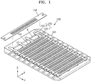
- FIG. 1 is a perspective view of a mask assembly 150 according to an embodiment.
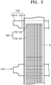
- FIG. 2 is a plan view of a mask sheet and a thin shielding plate of the mask assembly illustrated in FIG. 1 .
- FIG. 3 is a cross-sectional view of an apparatus 100 for manufacturing a display device including the mask assembly illustrated in FIG. 1 .
- the mask assembly 150 may include mask frames 151, a mask sheet 152, a thin shielding plate 153, and a support frame 154.
- a plurality of openings 152-1 may be arranged in the mask sheet 152 in a lengthwise direction of the mask sheet 152.
- the plurality of openings 152-1 may be spaced apart from each other by a predetermined interval and may substantially occupy an entire surface of the mask sheet 152.
- the thin shielding plate 153 may be installed on the mask frame 151.
- the thin shielding plate 153 may be a plurality of thin shielding plates, which may be installed on the mask frame 151 such that the thin shielding plates 153 are spaced apart from each other.
- the deposition region S may be defined by an area between the thin shielding plates 153.
- the deposition region S may have a shape other than a rectangle or a square.
- the shape of the deposition region S in plan view may be a triangle, a polygon, an ellipse, or a circle.
- the thin shielding plate 153 may include a thin shielding plate body portion 153-1 installed on the mask frame 151, and a first shielding portion 153-2 protruding from the thin shielding plate body portion 153-1.
- the thin shielding plate body portion 153-1 may include a straight line-shaped or linear plate.
- the thin shielding plate body portion 153-1 may be arranged in a direction (or a first direction) perpendicular to a lengthwise direction of the mask sheet 152, e.g. to extend along the Y-axis direction of FIG. 1 .
- the first shielding portion 153-2 may protrude in a lengthwise direction of the mask sheet 152 from the thin shielding plate body portion 153-1.
- the first shielding portion 153-2 may define an edge of the shape of the deposition region S with the thin shielding plate body portion 153-1.
- the first shielding portion 153-2 may define a portion of the edge of the deposition region S, and may form a predetermined angle with the thin shielding plate body portion 153-1, a curved portion, etc.
- the first shielding portion 153-2 may shield a portion of the plurality of openings 152-1 in the deposition region S.
- the first shielding portion 153-2 may shield a portion of the second openings 152-1 B near the edge (or the boundary) of the deposition region S.
- a deposition material may pass through only a portion of the second openings 152-1 B.
- the thin shielding plate 153 and the mask sheet 152 may include materials different from each other.
- the thin shielding plate 153 may include austenitic stainless steels
- the mask sheet 152 may include a nickel-steel alloy (such as, e.g., Invar).
- the thin shielding plate 153 and the mask sheet 152 may be fixed to the mask frame 151 while the thin shielding plate 153 and the mask sheet 152 are extended. In this case, the thin shielding plate 153 and the mask sheet 152 may be fixed to the mask frame 151 via welding.
- a support frame 154 may be provided between adjacent mask sheets 152. Both ends of the support frame 154 may be inserted into the mask frame 151. In this case, the support frame 154 may shield an interval between the mask sheets 152 and may also support the mask sheets 152, thereby preventing sagging of the mask sheets 152.
- An apparatus 100 for manufacturing a display device may include a chamber 110, a first support 120, a second support 130, the mask assembly 150, a source unit 140, a magnetic field generating unit 160, a vision unit 170, and a pressure adjustor 180.
- the chamber 110 may include a space therein, and the chamber 110 may have an opening.
- a gate valve 110-1 may be installed on the opening of the chamber 110 and the chamber 110 may be opened or closed by an operation of the gate valve 110-1.
- the first support 120 may accommodate a display substrate D thereon and support the display substrate D.
- the second support 130 may carry the mask assembly 150 thereon.
- the second support 130 may be inside the chamber 110.
- the second support 130 may fine-adjust the location of the mask assembly 150.
- the second support 130 may include a separate driver or alignment unit, etc. for moving the mask assembly 150 in different directions.
- the vision unit 170 may be installed on the chamber 110 and may capture locations of the display substrate D and the mask assembly 150.
- the vision unit 170 may include a camera capturing the display substrate D and the mask assembly 150.
- the locations of the display substrate D and the mask assembly 150 may be recognized based on an image captured by the vision unit 170.
- the second support 130 may then fine-adjust the location of the mask assembly 150 based on the image.
- the pressure adjustor 180 may be connected to the chamber 110, and may adjust the pressure of the atmosphere inside of the chamber 110.
- the pressure adjustor 180 may adjust the pressure of the inside of the chamber 110 to a pressure level the same as or similar to atmospheric pressure.
- the pressure adjustor 180 may adjust the pressure of the inside of the chamber 110 to a level the same as or similar to that of a vacuum state.
- the pressure adjustor 180 may include a connection pipe 181 connected to the chamber 110, and a pump 182 installed on the connection pipe 181.
- external air may be introduced via the connection pipe 181, or a gas inside the chamber 110 may be guided to the outside via the connection pipe 181 depending on an operation of the pump 182.
- the apparatus 100 for manufacturing the display device may be used to manufacture a display device (not shown) which will be described below.
- the pressure adjustor 180 adjusts the pressure inside the chamber 110 to a level which is the same as or similar to atmospheric pressure
- the gate valve 110-1 may operate to open the chamber 110.
- the display substrate D may be inserted from the outside of the chamber 110 into the inside of the chamber 110.
- the display substrate D may be inserted into the chamber 110 by various methods.
- the display substrate D may be inserted into the chamber 110 via a robot arm, etc. provided outside the chamber 110.
- the first support 120 in the case where the first support 120 has a shuttle form, the first support 120 is carried out from the inside of the chamber 110 to the outside of the chamber 110, and then the display substrate D is seated above the first support 120 via a separate robot arm, etc. provided outside the chamber 110. Subsequently, the first support 120 is inserted from the outside of the chamber 110 into the inside of the chamber 110.
- a case where the display substrate D is inserted from the outside of the chamber 110 into the inside of the chamber 110 via a robot arm provided outside the chamber 110 is mainly described.
- the source unit 140 may operate and supply the deposition material to the mask assembly 150.
- the deposition material that has passed through the plurality of openings 152-1 may be deposited on the display substrate D.
- the pump 182 may maintain the pressure inside the chamber 110 at a level which is the same as or similar to that of a vacuum state, by pumping a gas out of the chamber 110 and discharging the same.
- the deposition material may pass through the first openings 152-1A in the deposition region S, and may be deposited on the display substrate D. Also, the deposition material may pass through a portion of the second openings 152-1B at the edge of the deposition region S, and may be deposited on the display substrate D. In this case, the deposition region S may have a shape different from a rectangle or a square.
- the mask assembly 150, the apparatus 100 for manufacturing the display device, and a method of manufacturing the display device may be used to deposit a display area having a shape other than a rectangle or a square on the display substrate D.
- the display device manufactured via the mask assembly 150 the apparatus 100 for manufacturing the display device, and the method of manufacturing the display device are described.
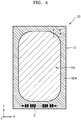
- FIG. 4 is a plan view of a display device manufactured by the apparatus illustrated in FIG. 3 .
- FIG. 5 is a cross-sectional view of the display device of FIG. 4 taken along a line V-V' of FIG. 4 .
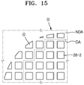
- FIG. 6 is a plan view illustrating the arrangement of an intermediate layer and a dummy intermediate layer illustrated in FIG. 5 .
- the substrate 21 may include a plastic material and may include a metallic material such as steel use stainless (SUS) or Ti. Also, the substrate 21 may include polyimide (PI). Hereinafter, for convenience of description, a case where the substrate 21 includes PI is mainly described.
- the TFT may be above the substrate 21, the passivation layer 27 may cover the TFT, and an organic light-emitting diode (OLED) 28 may be provided above the passivation layer 27.
- OLED organic light-emitting diode
- a pixel-defining layer 29 including an organic material and/or an inorganic material is formed so as to cover the pixel electrode 28-1 and the passivation layer 27.
- the pixel electrode 28-1 is exposed.
- the pixel electrode 28-1 and the opposite electrode 28-3 are insulated from each other by the intermediate layer 28-2, and light is emitted from an organic emission layer by applying voltages of different polarities to the intermediate layer 28-2.
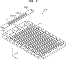
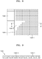
- a portion of the openings 152A-1 facing the support frame 154A may be formed by etching.
- the openings 152A-1 may be formed by performing etching twice when needed.
- one side of the second shielding portion 152A-3 may be formed after the first etching is made when forming the openings 152A-1. Therefore, the second shielding portion 152A-3 may have a variable thickness comprising areas having a thickness less than that of the rest of mask sheet 152A.
- the second shielding portion 152A-3 may have a first surface, which is flat, and a second surface opposite to the first surface comprising concave portions. The concave portions may be formed during the first etching or the second etching when forming the openings 152A-1.
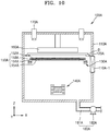
- the display substrate D is inserted into the chamber 110A and then the mask assembly 150A is arranged to face the display substrate D.
- the mask assembly 150A, the apparatus 100A for manufacturing the display device, and the method of manufacturing the display device may be used to deposit a shape which is not a rectangle or a square. Also, the mask assembly 150A, the apparatus 100A for manufacturing the display device, and the method of manufacturing the display device may improve deposition efficiency and deposition accuracy by making a more uniform interval between the display substrate D and the mask sheet 152A. The mask assembly 150A, the apparatus 100A for manufacturing the display device, and the method of manufacturing the display device may be used together to minimize deposition defects occurring during deposition.
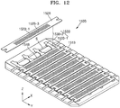
- the second shielding portion 152B-3 may shield a portion of the plurality of openings 152B-1.
- the second shielding portion 152B-3 may shield at least one opening 152B-1 arranged at the boundary of the first shielding portion 153B-2.
Landscapes
- Chemical & Material Sciences (AREA)
- Engineering & Computer Science (AREA)
- Metallurgy (AREA)
- Chemical Kinetics & Catalysis (AREA)
- Materials Engineering (AREA)
- Mechanical Engineering (AREA)
- Organic Chemistry (AREA)
- Manufacturing & Machinery (AREA)
- Microelectronics & Electronic Packaging (AREA)
- Physics & Mathematics (AREA)
- Geometry (AREA)
- Electroluminescent Light Sources (AREA)
- Physical Vapour Deposition (AREA)
- Devices For Indicating Variable Information By Combining Individual Elements (AREA)
Priority Applications (1)
| Application Number | Priority Date | Filing Date | Title |
|---|---|---|---|
| EP20193778.6A EP3767003A1 (de) | 2016-08-08 | 2017-08-07 | Anzeigevorrichtung |
Applications Claiming Priority (1)
| Application Number | Priority Date | Filing Date | Title |
|---|---|---|---|
| KR1020160100880A KR102632617B1 (ko) | 2016-08-08 | 2016-08-08 | 마스크 조립체, 이를 이용한 표시 장치의 제조장치, 이를 이용한 표시 장치의 제조방법 및 표시 장치 |
Related Child Applications (2)
| Application Number | Title | Priority Date | Filing Date |
|---|---|---|---|
| EP20193778.6A Division EP3767003A1 (de) | 2016-08-08 | 2017-08-07 | Anzeigevorrichtung |
| EP20193778.6A Division-Into EP3767003A1 (de) | 2016-08-08 | 2017-08-07 | Anzeigevorrichtung |
Publications (3)
| Publication Number | Publication Date |
|---|---|
| EP3282035A2 true EP3282035A2 (de) | 2018-02-14 |
| EP3282035A3 EP3282035A3 (de) | 2018-02-21 |
| EP3282035B1 EP3282035B1 (de) | 2020-10-07 |
Family
ID=59745148
Family Applications (2)
| Application Number | Title | Priority Date | Filing Date |
|---|---|---|---|
| EP20193778.6A Pending EP3767003A1 (de) | 2016-08-08 | 2017-08-07 | Anzeigevorrichtung |
| EP17185095.1A Active EP3282035B1 (de) | 2016-08-08 | 2017-08-07 | Maskenanordnung |
Family Applications Before (1)
| Application Number | Title | Priority Date | Filing Date |
|---|---|---|---|
| EP20193778.6A Pending EP3767003A1 (de) | 2016-08-08 | 2017-08-07 | Anzeigevorrichtung |
Country Status (5)
| Country | Link |
|---|---|
| US (2) | US10818877B2 (de) |
| EP (2) | EP3767003A1 (de) |
| JP (1) | JP6993804B2 (de) |
| KR (2) | KR102632617B1 (de) |
| CN (2) | CN114369793A (de) |
Cited By (3)
| Publication number | Priority date | Publication date | Assignee | Title |
|---|---|---|---|---|
| EP3594377A1 (de) * | 2018-06-15 | 2020-01-15 | Samsung Display Co., Ltd. | Maskenanordnung, ablagerungsvorrichtung damit und verfahren zur herstellung einer anzeigevorrichtung mit verwendung davon |
| EP3666920A1 (de) * | 2018-12-14 | 2020-06-17 | Samsung Display Co., Ltd. | Metallmaske, verfahren zu ihrer herstellung und verfahren zur herstellung einer anzeigetafel |
| EP3882369A4 (de) * | 2018-11-12 | 2022-08-10 | Boe Technology Group Co., Ltd. | Maske und verfahren zu ihrer herstellung |
Families Citing this family (38)
| Publication number | Priority date | Publication date | Assignee | Title |
|---|---|---|---|---|
| CN106480404B (zh) * | 2016-12-28 | 2019-05-03 | 京东方科技集团股份有限公司 | 一种掩膜集成框架及蒸镀装置 |
| CN107740040B (zh) | 2017-09-08 | 2019-09-24 | 上海天马有机发光显示技术有限公司 | 掩膜版组件及蒸镀装置 |
| CN107742623B (zh) * | 2017-11-15 | 2024-01-23 | 京东方科技集团股份有限公司 | 显示基板、有机发光器件及膜层蒸镀检测方法、显示装置 |
| KR102504135B1 (ko) * | 2018-03-08 | 2023-02-28 | 삼성디스플레이 주식회사 | 마스크 조립체, 마스크 조립체의 제조방법 및 표시 장치의 제조방법 |
| CN110343999B (zh) * | 2018-04-02 | 2021-10-12 | 京东方科技集团股份有限公司 | 掩模装置及其制造方法、蒸镀方法 |
| KR102191388B1 (ko) * | 2018-06-12 | 2020-12-15 | 어플라이드 머티어리얼스, 인코포레이티드 | 마스크프레임 및 마스크조립체 |
| KR102630638B1 (ko) * | 2018-08-29 | 2024-01-30 | 삼성디스플레이 주식회사 | 마스크 조립체, 표시 장치의 제조장치 및 표시 장치의 제조방법 |
| KR102618039B1 (ko) * | 2018-08-29 | 2023-12-27 | 삼성디스플레이 주식회사 | 마스크 조립체, 이를 포함한 표시 장치의 제조장치 및 표시 장치의 제조방법 |
| WO2020065955A1 (ja) * | 2018-09-28 | 2020-04-02 | シャープ株式会社 | 表示装置およびその製造方法 |
| KR102796879B1 (ko) * | 2018-10-02 | 2025-04-21 | 삼성디스플레이 주식회사 | 증착 장치 |
| KR102690567B1 (ko) * | 2018-10-02 | 2024-08-01 | 삼성디스플레이 주식회사 | 증착 장치 |
| KR20200039901A (ko) * | 2018-10-05 | 2020-04-17 | 삼성디스플레이 주식회사 | 박막 증착용 마스크 프레임 어셈블리 |
| KR102568785B1 (ko) * | 2018-11-02 | 2023-08-22 | 삼성디스플레이 주식회사 | 유기 발광 표시 장치의 제조 방법 및 마스크 조립체 |
| JP7406717B2 (ja) | 2018-12-25 | 2023-12-28 | 大日本印刷株式会社 | 蒸着マスク |
| US11773477B2 (en) | 2018-12-25 | 2023-10-03 | Dai Nippon Printing Co., Ltd. | Deposition mask |
| KR102711116B1 (ko) * | 2019-01-24 | 2024-09-27 | 삼성디스플레이 주식회사 | 표시장치 제조를 위한 마스크유닛 |
| KR20200092524A (ko) * | 2019-01-24 | 2020-08-04 | 삼성디스플레이 주식회사 | 박막 증착용 마스크 프레임 어셈블리 |
| JP7487481B2 (ja) | 2019-02-06 | 2024-05-21 | 大日本印刷株式会社 | 蒸着マスク装置、マスク支持機構及び蒸着マスク装置の製造方法 |
| KR102801662B1 (ko) * | 2019-04-16 | 2025-04-30 | 삼성디스플레이 주식회사 | 폴딩 가능한 디스플레이 장치 및 그 제조방법 |
| KR102724586B1 (ko) * | 2019-05-13 | 2024-11-01 | 삼성디스플레이 주식회사 | 마스크 어셈블리 및 이를 포함하는 증착설비 |
| KR20210009479A (ko) * | 2019-07-16 | 2021-01-27 | 삼성디스플레이 주식회사 | 표시 장치, 표시 장치의 제조장치 및 표시 장치의 제조방법 |
| KR102932280B1 (ko) * | 2019-07-25 | 2026-02-27 | 삼성디스플레이 주식회사 | 표시 장치, 표시 장치의 제조장치 및 표시 장치의 제조방법 |
| CN110438446B (zh) * | 2019-07-31 | 2020-12-29 | 昆山国显光电有限公司 | 一种掩模组件以及一种显示装置 |
| KR102889640B1 (ko) * | 2019-10-15 | 2025-11-21 | 삼성디스플레이 주식회사 | 표시 장치 |
| KR20210044947A (ko) * | 2019-10-15 | 2021-04-26 | 삼성디스플레이 주식회사 | 마스크 조립체, 표시 장치의 제조장치 및 표시 장치의 제조방법 |
| WO2021092759A1 (zh) * | 2019-11-12 | 2021-05-20 | 京东方科技集团股份有限公司 | 掩模板 |
| KR102818641B1 (ko) | 2020-01-06 | 2025-06-11 | 삼성디스플레이 주식회사 | 표시 장치의 제조장치 및 표시 장치의 제조방법 |
| KR102778477B1 (ko) * | 2020-01-20 | 2025-03-12 | 삼성디스플레이 주식회사 | 표시 장치의 제조장치 |
| KR102787865B1 (ko) * | 2020-02-21 | 2025-04-01 | 삼성디스플레이 주식회사 | 표시 장치의 제조장치, 마스크 어셈블리의 제조방법, 및 표시 장치의 제조방법 |
| US11613802B2 (en) * | 2020-04-17 | 2023-03-28 | Rockwell Collins, Inc. | Additively manufactured shadow masks for material deposition control |
| CN111769214B (zh) * | 2020-06-22 | 2022-10-04 | 武汉华星光电半导体显示技术有限公司 | 掩膜板及其制作方法 |
| CN111575648B (zh) * | 2020-06-23 | 2022-07-15 | 京东方科技集团股份有限公司 | 掩膜板组件及其制造方法 |
| KR102836944B1 (ko) * | 2020-06-29 | 2025-07-22 | 삼성디스플레이 주식회사 | 마스크 검사 장치 및 마스크 검사 방법 |
| KR102820735B1 (ko) | 2020-07-14 | 2025-06-16 | 삼성디스플레이 주식회사 | 표시 장치 |
| KR20220018140A (ko) * | 2020-08-05 | 2022-02-15 | 삼성디스플레이 주식회사 | 광조사장치 및 이의 제조방법 |
| US11781210B2 (en) * | 2021-03-09 | 2023-10-10 | Samsung Display Co., Ltd. | Magnet assembly and deposition apparatus including the same |
| CN113078279A (zh) * | 2021-03-30 | 2021-07-06 | 京东方科技集团股份有限公司 | 一种掩膜版 |
| CN115627444B (zh) * | 2022-11-02 | 2024-09-24 | 合肥维信诺科技有限公司 | 掩膜版组件及掩膜版组件的搬运方法 |
Family Cites Families (40)
| Publication number | Priority date | Publication date | Assignee | Title |
|---|---|---|---|---|
| US6221563B1 (en) * | 1999-08-12 | 2001-04-24 | Eastman Kodak Company | Method of making an organic electroluminescent device |
| US7183582B2 (en) | 2002-05-29 | 2007-02-27 | Seiko Epson Coporation | Electro-optical device and method of manufacturing the same, element driving device and method of manufacturing the same, element substrate, and electronic apparatus |
| JP2004055231A (ja) | 2002-07-17 | 2004-02-19 | Dainippon Printing Co Ltd | 有機el素子製造に用いる真空蒸着用多面付けメタルマスク |
| JP4506214B2 (ja) * | 2003-03-13 | 2010-07-21 | 東レ株式会社 | 有機電界発光装置およびその製造方法 |
| EP1605732A4 (de) * | 2003-03-17 | 2008-04-09 | Fujifilm Corp | Organische elektrolumineszenzanzeige undverfahren zu ihrer herstellung |
| KR100552972B1 (ko) * | 2003-10-09 | 2006-02-15 | 삼성에스디아이 주식회사 | 평판표시장치 및 그의 제조방법 |
| JP4608874B2 (ja) | 2003-12-02 | 2011-01-12 | ソニー株式会社 | 蒸着マスクおよびその製造方法 |
| WO2007034599A1 (ja) * | 2005-09-26 | 2007-03-29 | Sharp Kabushiki Kaisha | 表示装置 |
| KR20080045886A (ko) * | 2006-11-21 | 2008-05-26 | 삼성전자주식회사 | 유기막 증착용 마스크 및 그 제조방법, 이를 포함하는유기전계 발광표시장치의 제조방법 |
| KR20090059225A (ko) * | 2007-12-06 | 2009-06-11 | 엘지디스플레이 주식회사 | 분할 마스크 |
| KR101073561B1 (ko) * | 2009-02-05 | 2011-10-17 | 삼성모바일디스플레이주식회사 | 유기전계발광소자 및 그의 제조 방법 |
| KR101097305B1 (ko) | 2009-03-09 | 2011-12-23 | 삼성모바일디스플레이주식회사 | 더미 슬릿부를 차단하는 차단부를 구비한 고정세 증착 마스크, 상기 고정세 증착 마스크를 이용한 유기 발광 소자의 제조 방법, 및 상기 제조 방법에 의해 제조된 유기 발광 소자 |
| KR20120022135A (ko) * | 2010-09-01 | 2012-03-12 | 엘지디스플레이 주식회사 | 마스크 및 이를 이용한 증착 방법 |
| CN103237916B (zh) * | 2010-12-03 | 2015-07-22 | 夏普株式会社 | 蒸镀装置和回收装置 |
| KR101742816B1 (ko) | 2010-12-20 | 2017-06-02 | 삼성디스플레이 주식회사 | 마스크 프레임 조립체, 이의 제조 방법 및 이를 이용한 유기 발광 표시 장치의 제조 방법 |
| JP5291839B2 (ja) * | 2010-12-21 | 2013-09-18 | シャープ株式会社 | 蒸着装置及び蒸着方法 |
| KR101837624B1 (ko) * | 2011-05-06 | 2018-03-13 | 삼성디스플레이 주식회사 | 박막 증착용 마스크 프레임 조립체 및 그 제조방법 |
| KR20120131548A (ko) * | 2011-05-25 | 2012-12-05 | 삼성디스플레이 주식회사 | 유기층 증착 장치 |
| KR20130007005A (ko) * | 2011-06-28 | 2013-01-18 | 삼성디스플레이 주식회사 | 패턴 형성용 마스크 및 유기 발광 표시 장치 |
| TWI687315B (zh) * | 2012-01-12 | 2020-03-11 | 日商大日本印刷股份有限公司 | 蒸鍍遮罩、圖案之製造方法、有機半導體元件的製造方法 |
| US20130214388A1 (en) * | 2012-02-20 | 2013-08-22 | Texas Instruments Incorporated | Semiconductor Wafer Adapted to Support Transparency in Partial Wafer Processing |
| WO2014142183A1 (ja) * | 2013-03-15 | 2014-09-18 | シャープ株式会社 | アクティブマトリクス基板、アクティブマトリクス基板の製造方法、及び表示パネル |
| KR102072077B1 (ko) * | 2013-04-15 | 2020-02-03 | 삼성디스플레이 주식회사 | 유기 발광 표시 장치 및 그 제조 방법 |
| KR102061684B1 (ko) * | 2013-04-29 | 2020-01-03 | 삼성디스플레이 주식회사 | 표시패널 |
| KR102097443B1 (ko) * | 2013-05-09 | 2020-04-07 | 삼성디스플레이 주식회사 | 유기 발광 표시 장치 및 그 제조 방법 |
| KR102105077B1 (ko) * | 2013-07-01 | 2020-06-01 | 삼성디스플레이 주식회사 | 유기발광 디스플레이 장치 및 그 제조방법 |
| KR102106333B1 (ko) * | 2013-07-08 | 2020-05-06 | 삼성디스플레이 주식회사 | 마스크 조립체 및 이를 이용한 유기 발광 표시 장치의 제조 방법 |
| JP6114664B2 (ja) * | 2013-08-29 | 2017-04-12 | 株式会社ジャパンディスプレイ | 有機el表示装置 |
| KR102282996B1 (ko) * | 2013-10-30 | 2021-07-29 | 삼성디스플레이 주식회사 | 유기 발광 표시 장치 및 그의 제조 방법 |
| KR102219210B1 (ko) * | 2013-12-18 | 2021-02-23 | 삼성디스플레이 주식회사 | 단위 마스크 및 마스크 조립체 |
| KR102218644B1 (ko) * | 2013-12-19 | 2021-02-23 | 삼성디스플레이 주식회사 | 증착 장치 |
| KR102237428B1 (ko) * | 2014-02-14 | 2021-04-08 | 삼성디스플레이 주식회사 | 마스크 프레임 조립체 및 그 제조방법 |
| JP6369799B2 (ja) * | 2014-04-23 | 2018-08-08 | Tianma Japan株式会社 | 画素アレイ及び電気光学装置並びに電気機器 |
| KR20150135722A (ko) * | 2014-05-23 | 2015-12-03 | 삼성디스플레이 주식회사 | 유기발광 디스플레이 장치 및 그 제조방법 |
| KR20150141338A (ko) | 2014-06-10 | 2015-12-18 | 엘지디스플레이 주식회사 | 유기 발광 표시 장치 및 이의 제조 방법 |
| KR102273049B1 (ko) | 2014-07-04 | 2021-07-06 | 삼성디스플레이 주식회사 | 박막 증착용 마스크 프레임 어셈블리 |
| KR102162257B1 (ko) * | 2014-07-31 | 2020-10-07 | 엘지디스플레이 주식회사 | 디스플레이 장치 |
| KR102293507B1 (ko) * | 2014-12-08 | 2021-08-24 | 엘지디스플레이 주식회사 | 유기 발광 표시 장치 및 이를 제조하기 위한 박막 증착용 마스크 |
| KR102541449B1 (ko) | 2015-12-22 | 2023-06-09 | 삼성디스플레이 주식회사 | 박막 증착용 마스크 어셈블리 |
| KR102420460B1 (ko) | 2016-01-15 | 2022-07-14 | 삼성디스플레이 주식회사 | 마스크 프레임 조립체, 표시 장치의 제조 장치 및 표시 장치의 제조 방법 |
-
2016
- 2016-08-08 KR KR1020160100880A patent/KR102632617B1/ko active Active
-
2017
- 2017-07-17 US US15/651,808 patent/US10818877B2/en active Active
- 2017-07-31 JP JP2017148027A patent/JP6993804B2/ja active Active
- 2017-08-04 CN CN202210048872.XA patent/CN114369793A/zh active Pending
- 2017-08-04 CN CN201710659182.7A patent/CN107699851B/zh active Active
- 2017-08-07 EP EP20193778.6A patent/EP3767003A1/de active Pending
- 2017-08-07 EP EP17185095.1A patent/EP3282035B1/de active Active
-
2020
- 2020-10-05 US US17/063,676 patent/US11569487B2/en active Active
-
2024
- 2024-01-26 KR KR1020240012442A patent/KR102784718B1/ko active Active
Non-Patent Citations (1)
| Title |
|---|
| None |
Cited By (5)
| Publication number | Priority date | Publication date | Assignee | Title |
|---|---|---|---|---|
| EP3594377A1 (de) * | 2018-06-15 | 2020-01-15 | Samsung Display Co., Ltd. | Maskenanordnung, ablagerungsvorrichtung damit und verfahren zur herstellung einer anzeigevorrichtung mit verwendung davon |
| US11171288B2 (en) | 2018-06-15 | 2021-11-09 | Samsung Display Co., Ltd. | Mask assembly, deposition apparatus having the same, and method of fabricating display device using the same |
| EP3882369A4 (de) * | 2018-11-12 | 2022-08-10 | Boe Technology Group Co., Ltd. | Maske und verfahren zu ihrer herstellung |
| US12221684B2 (en) | 2018-11-12 | 2025-02-11 | Boe Technology Group Co., Ltd. | Mask plate and manufacturing method thereof |
| EP3666920A1 (de) * | 2018-12-14 | 2020-06-17 | Samsung Display Co., Ltd. | Metallmaske, verfahren zu ihrer herstellung und verfahren zur herstellung einer anzeigetafel |
Also Published As
| Publication number | Publication date |
|---|---|
| EP3767003A1 (de) | 2021-01-20 |
| US20180040857A1 (en) | 2018-02-08 |
| EP3282035B1 (de) | 2020-10-07 |
| JP6993804B2 (ja) | 2022-01-14 |
| KR20180017301A (ko) | 2018-02-21 |
| KR102632617B1 (ko) | 2024-02-02 |
| CN107699851B (zh) | 2022-02-08 |
| CN107699851A (zh) | 2018-02-16 |
| US11569487B2 (en) | 2023-01-31 |
| KR102784718B1 (ko) | 2025-03-24 |
| JP2018026344A (ja) | 2018-02-15 |
| EP3282035A3 (de) | 2018-02-21 |
| US10818877B2 (en) | 2020-10-27 |
| KR20240018545A (ko) | 2024-02-13 |
| CN114369793A (zh) | 2022-04-19 |
| US20210020874A1 (en) | 2021-01-21 |
Similar Documents
| Publication | Publication Date | Title |
|---|---|---|
| US11569487B2 (en) | Mask assembly, apparatus and method of manufacturing display device using the same, and display device | |
| US10224350B2 (en) | Mask for deposition, apparatus for manufacturing display apparatus having the same, and method of manufacturing display apparatus with manufacturing display apparatus having mask for deposition | |
| US9997708B2 (en) | Mask frame assembly, apparatus and method for manufacturing a display apparatus | |
| KR102424976B1 (ko) | 마스크 조립체, 이를 이용한 표시 장치의 제조장치 및 표시 장치의 제조방법 | |
| US9999943B2 (en) | Method of manufacturing a mask | |
| KR102444178B1 (ko) | 마스크 조립체, 마스크 조립체 제조방법 및 표시 장치 제조방법 | |
| KR102630638B1 (ko) | 마스크 조립체, 표시 장치의 제조장치 및 표시 장치의 제조방법 | |
| US10790447B2 (en) | Mask for thin film deposition, method of manufacturing the same, and method of manufacturing a display apparatus using the same | |
| US11678558B2 (en) | Mask assembly and apparatus and method of manufacturing display apparatus | |
| KR102606276B1 (ko) | 마스크 조립체의 제조방법 및 표시 장치의 제조방법 | |
| KR102411539B1 (ko) | 마스크 조립체, 표시 장치의 제조장치 및 표시 장치의 제조방법 | |
| KR102504135B1 (ko) | 마스크 조립체, 마스크 조립체의 제조방법 및 표시 장치의 제조방법 | |
| KR102427674B1 (ko) | 마스크 조립체 및 이를 이용한 표시 장치의 제조장치 | |
| US9803279B2 (en) | Apparatus and method for manufacturing display apparatus | |
| US8936958B2 (en) | Method of manufacturing organic light emitting display apparatus | |
| KR20260055501A (ko) | 얼라인먼트 장치, 얼라인먼트 방법, 성막 장치 및 제조방법 | |
| KR20230016097A (ko) | 마스크 조립체, 표시 장치의 제조장치 및 표시 장치의 제조방법 | |
| CN117769336A (zh) | 制造显示装置的设备和制造显示装置的方法 | |
| KR20210116802A (ko) | 디스플레이 장치의 제조장치 및 디스플레이 장치의 제조방법 |
Legal Events
| Date | Code | Title | Description |
|---|---|---|---|
| PUAI | Public reference made under article 153(3) epc to a published international application that has entered the european phase |
Free format text: ORIGINAL CODE: 0009012 |
|
| STAA | Information on the status of an ep patent application or granted ep patent |
Free format text: STATUS: THE APPLICATION HAS BEEN PUBLISHED |
|
| PUAL | Search report despatched |
Free format text: ORIGINAL CODE: 0009013 |
|
| AK | Designated contracting states |
Kind code of ref document: A2 Designated state(s): AL AT BE BG CH CY CZ DE DK EE ES FI FR GB GR HR HU IE IS IT LI LT LU LV MC MK MT NL NO PL PT RO RS SE SI SK SM TR |
|
| AX | Request for extension of the european patent |
Extension state: BA ME |
|
| AK | Designated contracting states |
Kind code of ref document: A3 Designated state(s): AL AT BE BG CH CY CZ DE DK EE ES FI FR GB GR HR HU IE IS IT LI LT LU LV MC MK MT NL NO PL PT RO RS SE SI SK SM TR |
|
| AX | Request for extension of the european patent |
Extension state: BA ME |
|
| RIC1 | Information provided on ipc code assigned before grant |
Ipc: C23C 14/04 20060101AFI20180116BHEP Ipc: H01L 27/32 20060101ALI20180116BHEP Ipc: H01L 51/00 20060101ALI20180116BHEP |
|
| STAA | Information on the status of an ep patent application or granted ep patent |
Free format text: STATUS: REQUEST FOR EXAMINATION WAS MADE |
|
| 17P | Request for examination filed |
Effective date: 20180525 |
|
| RBV | Designated contracting states (corrected) |
Designated state(s): AL AT BE BG CH CY CZ DE DK EE ES FI FR GB GR HR HU IE IS IT LI LT LU LV MC MK MT NL NO PL PT RO RS SE SI SK SM TR |
|
| STAA | Information on the status of an ep patent application or granted ep patent |
Free format text: STATUS: EXAMINATION IS IN PROGRESS |
|
| 17Q | First examination report despatched |
Effective date: 20180911 |
|
| GRAJ | Information related to disapproval of communication of intention to grant by the applicant or resumption of examination proceedings by the epo deleted |
Free format text: ORIGINAL CODE: EPIDOSDIGR1 |
|
| GRAP | Despatch of communication of intention to grant a patent |
Free format text: ORIGINAL CODE: EPIDOSNIGR1 |
|
| GRAP | Despatch of communication of intention to grant a patent |
Free format text: ORIGINAL CODE: EPIDOSNIGR1 |
|
| STAA | Information on the status of an ep patent application or granted ep patent |
Free format text: STATUS: GRANT OF PATENT IS INTENDED |
|
| INTG | Intention to grant announced |
Effective date: 20200415 |
|
| GRAS | Grant fee paid |
Free format text: ORIGINAL CODE: EPIDOSNIGR3 |
|
| GRAA | (expected) grant |
Free format text: ORIGINAL CODE: 0009210 |
|
| STAA | Information on the status of an ep patent application or granted ep patent |
Free format text: STATUS: THE PATENT HAS BEEN GRANTED |
|
| AK | Designated contracting states |
Kind code of ref document: B1 Designated state(s): AL AT BE BG CH CY CZ DE DK EE ES FI FR GB GR HR HU IE IS IT LI LT LU LV MC MK MT NL NO PL PT RO RS SE SI SK SM TR |
|
| REG | Reference to a national code |
Ref country code: GB Ref legal event code: FG4D |
|
| REG | Reference to a national code |
Ref country code: CH Ref legal event code: EP Ref country code: AT Ref legal event code: REF Ref document number: 1321235 Country of ref document: AT Kind code of ref document: T Effective date: 20201015 |
|
| REG | Reference to a national code |
Ref country code: DE Ref legal event code: R096 Ref document number: 602017024897 Country of ref document: DE |
|
| REG | Reference to a national code |
Ref country code: IE Ref legal event code: FG4D |
|
| REG | Reference to a national code |
Ref country code: NL Ref legal event code: MP Effective date: 20201007 |
|
| REG | Reference to a national code |
Ref country code: AT Ref legal event code: MK05 Ref document number: 1321235 Country of ref document: AT Kind code of ref document: T Effective date: 20201007 |
|
| PG25 | Lapsed in a contracting state [announced via postgrant information from national office to epo] |
Ref country code: NL Free format text: LAPSE BECAUSE OF FAILURE TO SUBMIT A TRANSLATION OF THE DESCRIPTION OR TO PAY THE FEE WITHIN THE PRESCRIBED TIME-LIMIT Effective date: 20201007 Ref country code: NO Free format text: LAPSE BECAUSE OF FAILURE TO SUBMIT A TRANSLATION OF THE DESCRIPTION OR TO PAY THE FEE WITHIN THE PRESCRIBED TIME-LIMIT Effective date: 20210107 Ref country code: PT Free format text: LAPSE BECAUSE OF FAILURE TO SUBMIT A TRANSLATION OF THE DESCRIPTION OR TO PAY THE FEE WITHIN THE PRESCRIBED TIME-LIMIT Effective date: 20210208 Ref country code: RS Free format text: LAPSE BECAUSE OF FAILURE TO SUBMIT A TRANSLATION OF THE DESCRIPTION OR TO PAY THE FEE WITHIN THE PRESCRIBED TIME-LIMIT Effective date: 20201007 Ref country code: GR Free format text: LAPSE BECAUSE OF FAILURE TO SUBMIT A TRANSLATION OF THE DESCRIPTION OR TO PAY THE FEE WITHIN THE PRESCRIBED TIME-LIMIT Effective date: 20210108 Ref country code: FI Free format text: LAPSE BECAUSE OF FAILURE TO SUBMIT A TRANSLATION OF THE DESCRIPTION OR TO PAY THE FEE WITHIN THE PRESCRIBED TIME-LIMIT Effective date: 20201007 |
|
| REG | Reference to a national code |
Ref country code: LT Ref legal event code: MG4D |
|
| PG25 | Lapsed in a contracting state [announced via postgrant information from national office to epo] |
Ref country code: ES Free format text: LAPSE BECAUSE OF FAILURE TO SUBMIT A TRANSLATION OF THE DESCRIPTION OR TO PAY THE FEE WITHIN THE PRESCRIBED TIME-LIMIT Effective date: 20201007 Ref country code: AT Free format text: LAPSE BECAUSE OF FAILURE TO SUBMIT A TRANSLATION OF THE DESCRIPTION OR TO PAY THE FEE WITHIN THE PRESCRIBED TIME-LIMIT Effective date: 20201007 Ref country code: BG Free format text: LAPSE BECAUSE OF FAILURE TO SUBMIT A TRANSLATION OF THE DESCRIPTION OR TO PAY THE FEE WITHIN THE PRESCRIBED TIME-LIMIT Effective date: 20210107 Ref country code: LV Free format text: LAPSE BECAUSE OF FAILURE TO SUBMIT A TRANSLATION OF THE DESCRIPTION OR TO PAY THE FEE WITHIN THE PRESCRIBED TIME-LIMIT Effective date: 20201007 Ref country code: IS Free format text: LAPSE BECAUSE OF FAILURE TO SUBMIT A TRANSLATION OF THE DESCRIPTION OR TO PAY THE FEE WITHIN THE PRESCRIBED TIME-LIMIT Effective date: 20210207 Ref country code: PL Free format text: LAPSE BECAUSE OF FAILURE TO SUBMIT A TRANSLATION OF THE DESCRIPTION OR TO PAY THE FEE WITHIN THE PRESCRIBED TIME-LIMIT Effective date: 20201007 Ref country code: SE Free format text: LAPSE BECAUSE OF FAILURE TO SUBMIT A TRANSLATION OF THE DESCRIPTION OR TO PAY THE FEE WITHIN THE PRESCRIBED TIME-LIMIT Effective date: 20201007 |
|
| PG25 | Lapsed in a contracting state [announced via postgrant information from national office to epo] |
Ref country code: HR Free format text: LAPSE BECAUSE OF FAILURE TO SUBMIT A TRANSLATION OF THE DESCRIPTION OR TO PAY THE FEE WITHIN THE PRESCRIBED TIME-LIMIT Effective date: 20201007 |
|
| REG | Reference to a national code |
Ref country code: DE Ref legal event code: R097 Ref document number: 602017024897 Country of ref document: DE |
|
| PG25 | Lapsed in a contracting state [announced via postgrant information from national office to epo] |
Ref country code: CZ Free format text: LAPSE BECAUSE OF FAILURE TO SUBMIT A TRANSLATION OF THE DESCRIPTION OR TO PAY THE FEE WITHIN THE PRESCRIBED TIME-LIMIT Effective date: 20201007 Ref country code: EE Free format text: LAPSE BECAUSE OF FAILURE TO SUBMIT A TRANSLATION OF THE DESCRIPTION OR TO PAY THE FEE WITHIN THE PRESCRIBED TIME-LIMIT Effective date: 20201007 Ref country code: LT Free format text: LAPSE BECAUSE OF FAILURE TO SUBMIT A TRANSLATION OF THE DESCRIPTION OR TO PAY THE FEE WITHIN THE PRESCRIBED TIME-LIMIT Effective date: 20201007 Ref country code: SM Free format text: LAPSE BECAUSE OF FAILURE TO SUBMIT A TRANSLATION OF THE DESCRIPTION OR TO PAY THE FEE WITHIN THE PRESCRIBED TIME-LIMIT Effective date: 20201007 Ref country code: SK Free format text: LAPSE BECAUSE OF FAILURE TO SUBMIT A TRANSLATION OF THE DESCRIPTION OR TO PAY THE FEE WITHIN THE PRESCRIBED TIME-LIMIT Effective date: 20201007 Ref country code: RO Free format text: LAPSE BECAUSE OF FAILURE TO SUBMIT A TRANSLATION OF THE DESCRIPTION OR TO PAY THE FEE WITHIN THE PRESCRIBED TIME-LIMIT Effective date: 20201007 |
|
| PLBE | No opposition filed within time limit |
Free format text: ORIGINAL CODE: 0009261 |
|
| STAA | Information on the status of an ep patent application or granted ep patent |
Free format text: STATUS: NO OPPOSITION FILED WITHIN TIME LIMIT |
|
| PG25 | Lapsed in a contracting state [announced via postgrant information from national office to epo] |
Ref country code: DK Free format text: LAPSE BECAUSE OF FAILURE TO SUBMIT A TRANSLATION OF THE DESCRIPTION OR TO PAY THE FEE WITHIN THE PRESCRIBED TIME-LIMIT Effective date: 20201007 |
|
| 26N | No opposition filed |
Effective date: 20210708 |
|
| PG25 | Lapsed in a contracting state [announced via postgrant information from national office to epo] |
Ref country code: IT Free format text: LAPSE BECAUSE OF FAILURE TO SUBMIT A TRANSLATION OF THE DESCRIPTION OR TO PAY THE FEE WITHIN THE PRESCRIBED TIME-LIMIT Effective date: 20201007 Ref country code: AL Free format text: LAPSE BECAUSE OF FAILURE TO SUBMIT A TRANSLATION OF THE DESCRIPTION OR TO PAY THE FEE WITHIN THE PRESCRIBED TIME-LIMIT Effective date: 20201007 |
|
| PG25 | Lapsed in a contracting state [announced via postgrant information from national office to epo] |
Ref country code: SI Free format text: LAPSE BECAUSE OF FAILURE TO SUBMIT A TRANSLATION OF THE DESCRIPTION OR TO PAY THE FEE WITHIN THE PRESCRIBED TIME-LIMIT Effective date: 20201007 |
|
| REG | Reference to a national code |
Ref country code: CH Ref legal event code: PL |
|
| PG25 | Lapsed in a contracting state [announced via postgrant information from national office to epo] |
Ref country code: MC Free format text: LAPSE BECAUSE OF FAILURE TO SUBMIT A TRANSLATION OF THE DESCRIPTION OR TO PAY THE FEE WITHIN THE PRESCRIBED TIME-LIMIT Effective date: 20201007 |
|
| REG | Reference to a national code |
Ref country code: BE Ref legal event code: MM Effective date: 20210831 |
|
| PG25 | Lapsed in a contracting state [announced via postgrant information from national office to epo] |
Ref country code: LI Free format text: LAPSE BECAUSE OF NON-PAYMENT OF DUE FEES Effective date: 20210831 Ref country code: CH Free format text: LAPSE BECAUSE OF NON-PAYMENT OF DUE FEES Effective date: 20210831 |
|
| PG25 | Lapsed in a contracting state [announced via postgrant information from national office to epo] |
Ref country code: IS Free format text: LAPSE BECAUSE OF FAILURE TO SUBMIT A TRANSLATION OF THE DESCRIPTION OR TO PAY THE FEE WITHIN THE PRESCRIBED TIME-LIMIT Effective date: 20210207 Ref country code: LU Free format text: LAPSE BECAUSE OF NON-PAYMENT OF DUE FEES Effective date: 20210807 |
|
| PG25 | Lapsed in a contracting state [announced via postgrant information from national office to epo] |
Ref country code: IE Free format text: LAPSE BECAUSE OF NON-PAYMENT OF DUE FEES Effective date: 20210807 Ref country code: BE Free format text: LAPSE BECAUSE OF NON-PAYMENT OF DUE FEES Effective date: 20210831 |
|
| PG25 | Lapsed in a contracting state [announced via postgrant information from national office to epo] |
Ref country code: HU Free format text: LAPSE BECAUSE OF FAILURE TO SUBMIT A TRANSLATION OF THE DESCRIPTION OR TO PAY THE FEE WITHIN THE PRESCRIBED TIME-LIMIT; INVALID AB INITIO Effective date: 20170807 |
|
| P01 | Opt-out of the competence of the unified patent court (upc) registered |
Effective date: 20230516 |
|
| PG25 | Lapsed in a contracting state [announced via postgrant information from national office to epo] |
Ref country code: CY Free format text: LAPSE BECAUSE OF FAILURE TO SUBMIT A TRANSLATION OF THE DESCRIPTION OR TO PAY THE FEE WITHIN THE PRESCRIBED TIME-LIMIT Effective date: 20201007 |
|
| PG25 | Lapsed in a contracting state [announced via postgrant information from national office to epo] |
Ref country code: MK Free format text: LAPSE BECAUSE OF FAILURE TO SUBMIT A TRANSLATION OF THE DESCRIPTION OR TO PAY THE FEE WITHIN THE PRESCRIBED TIME-LIMIT Effective date: 20201007 |
|
| PG25 | Lapsed in a contracting state [announced via postgrant information from national office to epo] |
Ref country code: MT Free format text: LAPSE BECAUSE OF FAILURE TO SUBMIT A TRANSLATION OF THE DESCRIPTION OR TO PAY THE FEE WITHIN THE PRESCRIBED TIME-LIMIT Effective date: 20201007 |
|
| PGFP | Annual fee paid to national office [announced via postgrant information from national office to epo] |
Ref country code: DE Payment date: 20250721 Year of fee payment: 9 |
|
| PGFP | Annual fee paid to national office [announced via postgrant information from national office to epo] |
Ref country code: GB Payment date: 20250722 Year of fee payment: 9 |
|
| PGFP | Annual fee paid to national office [announced via postgrant information from national office to epo] |
Ref country code: FR Payment date: 20250725 Year of fee payment: 9 |
|
| PG25 | Lapsed in a contracting state [announced via postgrant information from national office to epo] |
Ref country code: TR Free format text: LAPSE BECAUSE OF FAILURE TO SUBMIT A TRANSLATION OF THE DESCRIPTION OR TO PAY THE FEE WITHIN THE PRESCRIBED TIME-LIMIT Effective date: 20201007 |