EP3282244A1 - Dispositif de détermination de la concentration d'un analyte dans un milieu gazeux - Google Patents
Dispositif de détermination de la concentration d'un analyte dans un milieu gazeux Download PDFInfo
- Publication number
- EP3282244A1 EP3282244A1 EP17183201.7A EP17183201A EP3282244A1 EP 3282244 A1 EP3282244 A1 EP 3282244A1 EP 17183201 A EP17183201 A EP 17183201A EP 3282244 A1 EP3282244 A1 EP 3282244A1
- Authority
- EP
- European Patent Office
- Prior art keywords
- sensor unit
- insulating layer
- housing
- analyte
- medium
- Prior art date
- Legal status (The legal status is an assumption and is not a legal conclusion. Google has not performed a legal analysis and makes no representation as to the accuracy of the status listed.)
- Granted
Links
Images

Classifications
-
- G—PHYSICS
- G01—MEASURING; TESTING
- G01N—INVESTIGATING OR ANALYSING MATERIALS BY DETERMINING THEIR CHEMICAL OR PHYSICAL PROPERTIES
- G01N33/00—Investigating or analysing materials by specific methods not covered by groups G01N1/00 - G01N31/00
- G01N33/0004—Gaseous mixtures, e.g. polluted air
- G01N33/0009—General constructional details of gas analysers, e.g. portable test equipment
- G01N33/0027—General constructional details of gas analysers, e.g. portable test equipment concerning the detector
-
- G—PHYSICS
- G01—MEASURING; TESTING
- G01N—INVESTIGATING OR ANALYSING MATERIALS BY DETERMINING THEIR CHEMICAL OR PHYSICAL PROPERTIES
- G01N21/00—Investigating or analysing materials by the use of optical means, i.e. using sub-millimetre waves, infrared, visible or ultraviolet light
- G01N21/62—Systems in which the material investigated is excited whereby it emits light or causes a change in wavelength of the incident light
- G01N21/63—Systems in which the material investigated is excited whereby it emits light or causes a change in wavelength of the incident light optically excited
-
- G—PHYSICS
- G01—MEASURING; TESTING
- G01N—INVESTIGATING OR ANALYSING MATERIALS BY DETERMINING THEIR CHEMICAL OR PHYSICAL PROPERTIES
- G01N21/00—Investigating or analysing materials by the use of optical means, i.e. using sub-millimetre waves, infrared, visible or ultraviolet light
- G01N21/75—Systems in which material is subjected to a chemical reaction, the progress or the result of the reaction being investigated
- G01N21/77—Systems in which material is subjected to a chemical reaction, the progress or the result of the reaction being investigated by observing the effect on a chemical indicator
- G01N21/78—Systems in which material is subjected to a chemical reaction, the progress or the result of the reaction being investigated by observing the effect on a chemical indicator producing a change of colour
- G01N21/783—Systems in which material is subjected to a chemical reaction, the progress or the result of the reaction being investigated by observing the effect on a chemical indicator producing a change of colour for analysing gases
-
- G—PHYSICS
- G01—MEASURING; TESTING
- G01N—INVESTIGATING OR ANALYSING MATERIALS BY DETERMINING THEIR CHEMICAL OR PHYSICAL PROPERTIES
- G01N21/00—Investigating or analysing materials by the use of optical means, i.e. using sub-millimetre waves, infrared, visible or ultraviolet light
- G01N21/75—Systems in which material is subjected to a chemical reaction, the progress or the result of the reaction being investigated
- G01N21/77—Systems in which material is subjected to a chemical reaction, the progress or the result of the reaction being investigated by observing the effect on a chemical indicator
- G01N21/7703—Systems in which material is subjected to a chemical reaction, the progress or the result of the reaction being investigated by observing the effect on a chemical indicator using reagent-clad optical fibres or optical waveguides
- G01N2021/7706—Reagent provision
- G01N2021/773—Porous polymer jacket; Polymer matrix with indicator
-
- G—PHYSICS
- G01—MEASURING; TESTING
- G01N—INVESTIGATING OR ANALYSING MATERIALS BY DETERMINING THEIR CHEMICAL OR PHYSICAL PROPERTIES
- G01N21/00—Investigating or analysing materials by the use of optical means, i.e. using sub-millimetre waves, infrared, visible or ultraviolet light
- G01N21/75—Systems in which material is subjected to a chemical reaction, the progress or the result of the reaction being investigated
- G01N21/77—Systems in which material is subjected to a chemical reaction, the progress or the result of the reaction being investigated by observing the effect on a chemical indicator
- G01N2021/775—Indicator and selective membrane
-
- G—PHYSICS
- G01—MEASURING; TESTING
- G01N—INVESTIGATING OR ANALYSING MATERIALS BY DETERMINING THEIR CHEMICAL OR PHYSICAL PROPERTIES
- G01N21/00—Investigating or analysing materials by the use of optical means, i.e. using sub-millimetre waves, infrared, visible or ultraviolet light
- G01N21/75—Systems in which material is subjected to a chemical reaction, the progress or the result of the reaction being investigated
- G01N21/77—Systems in which material is subjected to a chemical reaction, the progress or the result of the reaction being investigated by observing the effect on a chemical indicator
- G01N2021/7769—Measurement method of reaction-produced change in sensor
- G01N2021/7786—Fluorescence
-
- G—PHYSICS
- G01—MEASURING; TESTING
- G01N—INVESTIGATING OR ANALYSING MATERIALS BY DETERMINING THEIR CHEMICAL OR PHYSICAL PROPERTIES
- G01N21/00—Investigating or analysing materials by the use of optical means, i.e. using sub-millimetre waves, infrared, visible or ultraviolet light
- G01N21/62—Systems in which the material investigated is excited whereby it emits light or causes a change in wavelength of the incident light
- G01N21/63—Systems in which the material investigated is excited whereby it emits light or causes a change in wavelength of the incident light optically excited
- G01N21/64—Fluorescence; Phosphorescence
- G01N21/6428—Measuring fluorescence of fluorescent products of reactions or of fluorochrome labelled reactive substances, e.g. measuring quenching effects, using measuring "optrodes"
- G01N21/643—Measuring fluorescence of fluorescent products of reactions or of fluorochrome labelled reactive substances, e.g. measuring quenching effects, using measuring "optrodes" non-biological material
-
- G—PHYSICS
- G01—MEASURING; TESTING
- G01N—INVESTIGATING OR ANALYSING MATERIALS BY DETERMINING THEIR CHEMICAL OR PHYSICAL PROPERTIES
- G01N2201/00—Features of devices classified in G01N21/00
- G01N2201/12—Circuits of general importance; Signal processing
- G01N2201/121—Correction signals
- G01N2201/1211—Correction signals for temperature
Definitions
- a "light source” is understood to mean a device which is suitable for emitting light. This does not necessarily have to be light visible to the human eye. Instead, for example, it may also be an infrared radiation or an ultraviolet radiation. In particular, as an LED light source is conceivable.
- a "light receiver” is understood to mean a device which is suitable for converting received light radiation into specific information.
- a light receiver is suitable for converting the received light into an electrical voltage or an electric current.
- Such a light receiver may also be suitable in particular for light that the human eye can not process, for example an infrared radiation.
- a light receiver may be formed by a photodiode.
- an "optical sensor unit” is understood to mean a sensor unit which, by outputting optical information, permits a conclusion to be drawn about an analyte which has been examined in each case.
- these are, in particular, those sensor units whose optical properties change as a function of the respective state parameter, for example the concentration, of the respective analyte.
- a typical example of such a sensor unit is one which has luminescent properties, wherein the luminescence of the sensor unit changes as a function of the concentration of the respective analyte.
- a conclusion can be drawn as to which concentration of the analyte is present in the gaseous medium being investigated.
- luminescent sensor units absorbing sensor units and all other technically possible sensor units are also conceivable. An absorbing sensor unit absorbs different amounts of light as a function of the state parameter, so that a conclusion can be drawn on the state parameter of the analyte by examining an unabsorbed portion.
- a “housing” is understood to be a spatially dedicated area in which, at least as a rule, all electronic components of the device are accommodated.
- the housing may be open or closed, the latter may be particularly useful if a moisture in the housing and a concomitant damage to the electronic components of the device is feared.
- An open design can in particular offer the advantage of a pressure equalization between the components of the device and the environment.
- the housing may, in particular, have a partition which represents an immediate spatial separation between a medium space and an interior of the housing, wherein the medium and the sensor unit are located on the side of the medium space and the remaining components of the apparatus are arranged on the side of the interior space.
- the partition wall possibly the entire housing, may be formed by a transparent material, so that a passage of light through the partition wall is made possible.
- the sensor units of such devices typically consist of a luminescent chemical substance whose luminescence changes as a function of the concentration of the analyte.
- a light radiation is produced starting from the sensor unit, wherein properties of this radiation emanating from the sensor unit permit a conclusion on the concentration of the analyte in or on the sensor unit.
- a typical problem in determining the concentration of an analyte by means of an optical sensor unit is that this type of sensor unit has a particularly high sensitivity to changing temperatures. This sensitivity manifests itself in the fact that the luminescent properties of the sensor unit likewise change as a result of a change in the temperature. As a result, it is understandably not possible to draw from a change in the luminescence of the sensor unit readily a direct inference to the cause of this change, so that in particular no direct statement about the concentration of the analyte in the medium to be examined is possible.
- temperature sensors are used in the prior art that continuously monitor the temperature of the sensor unit.
- a change in the temperature of the sensor unit be detected as quickly as possible and thus taken into account in the context of the evaluation of the radiation emitted by the sensor unit.
- a certain time offset between the change in the temperature of the sensor unit and their must be granted by means of a temperature measuring means a certain transitional period must first be granted in the presence of a change in the temperature of the sensor unit, before a reliable statement about the concentration of each analyte examined is possible.
- the temperature of the sensor unit deviates as little as possible from the temperature detected by the temperature measuring means. Deviations can arise in particular due to different temperatures of the medium to be examined and of the housing. These deviations can have a negative influence on the accuracy of the measurement of the analyte.
- the underlying object is achieved, starting from the device of the type described above according to the invention by a thermal insulating layer, which is adapted to at least thermally separate the optical sensor unit from the medium to be examined.
- This separation should at least be such that temperature fluctuations of the media volume flow, if at all only greatly delayed, preferably not at all, are transmitted to the sensor unit.
- the insulating layer should also be any resulting temperature differences between the Minimize temperature measuring means inside the housing and the sensor unit outside the housing, preferably completely avoid.
- a "thermal insulation layer” is understood to be a layer whose primary purpose is to provide thermal insulation of the sensor unit from the medium to be examined.
- a thermal insulation layer is defined by their suitability to provide such thermal insulation can.
- insulating layers according to the prior art for example, those which are intended to ensure optical isolation of the respective sensor unit, not as "thermal insulation” within the meaning of the present application understandable, since these known insulating layers are not as well suited, since they have a Passing of thermal energy from one side of the respective layer to the other side hardly or can not prevent.
- each layer has a certain heat capacity that enables the layer to absorb some amount of thermal energy itself.
- the thermal insulation layer according to the invention is designed such that it has a heat capacity of at least 0.3 J / gK, preferably at least 0.5 J / gK, more preferably 0.8 J / gK.
- Such an insulating layer is particularly well suited to pass on a temperature of the medium to be examined to the sensor unit, since the insulating layer itself can be changed only relatively sluggish in their temperature.
- the thermal insulating layer must cooperate in such a way with the rest of the device, that an immediate passage of the examined media volume flow is prevented at the optical sensor unit, so that at least no significant immediate exchange of thermal energy, for example due to convection, between the Medium and the sensor unit is possible. If the latter were still present despite the thermal insulation layer, the insulating layer would in fact be ineffective. Consequently, it is understood that the insulating layer must be permeable at least in some way to the respective analyte to be examined, so that despite the shielding of the media volume flow of the optical sensor unit at least the migration of individual particles of the analyte from the medium to the optical sensor unit is made possible.
- the thermal insulation layer is porous, in particular porous porous.
- a diffusion of an analyte through a solid is also possible.
- a porous embodiment of the insulating layer is advantageous for generating the lowest possible heat transfer coefficient of the insulating layer.
- the device according to the invention has many advantages.
- it is ensured by the use of the thermal insulating layer that a change in the temperature of the medium in each case is passed on, if at all only greatly delayed to the sensor unit.
- a sudden change in the temperature of the sensor unit as it must be regularly feared in the prior art, thus can not occur.
- short-term fluctuations in the temperature of the medium being studied are almost or ideally even completely unaffected by the temperature of the sensor unit. Should it come to a long-term change in the temperature of the medium, it is understood that permanently the temperature of the sensor unit will adapt accordingly. Due to the thermal insulation layer, however, this change takes place only slowly and consequently controlled.
- the detection of such a slow change in the temperature of the sensor unit can be reliably determined by means of comparatively simple temperature measuring means, so that a reliable determination of the concentration of the analyte in the medium is continuously possible.
- a further advantage of the device according to the invention is that the at least one temperature measuring means which is used to determine the temperature of the optical sensor unit can be carried out in a particularly simple and consequently inexpensive manner.
- no expensive temperature measuring means is required that is suitable for detecting short-term temperature fluctuations of the sensor unit.
- the temperature measuring means can remain within the housing of the device, that is, at least arranged at a certain distance from the sensor unit, since the latter is outside the housing. Despite this "remote arrangement" of the temperature measuring means relative to the sensor unit can be made due to the only slow fluctuations in the temperature of the sensor unit in each case, a reliable statement about just that temperature.
- a thickness of the thermal insulation layer is at least 0.5 mm, preferably at least 1.0 mm, more preferably at least 1.5 mm.
- Such an insulating layer formed is particularly well suited to ensure sufficient thermal insulation between the medium and the sensor unit.
- such a device may be of particular advantage, in which the material of the insulating layer has a thermal conductivity of at most 0.7 W / mK, preferably at most 0.5 W / mK, more preferably at most 0.3 W / mK. It is understood that the use of such a material is particularly well suited to perform a thermal insulation function.
- the device of the invention further ausgestaltend the heat transfer coefficient of the insulating layer is at most 400 W / m 2 K, preferably at most 200 W / m 2 K, more preferably at most 100 W / m 2 K. It is basically irrelevant whether the heat transfer coefficient described so due to a certain thickness of the insulating layer or due to a particularly low thermal conductivity of the material used comes about. Ideally, the insulating layer has both a certain thickness, a comparatively low thermal conductivity and a comparatively high heat capacity.
- the insulating layer is formed of a hydrophobic material, preferably of polytetrafluoroethylene (PTFE), in particular of sintered polytetrafluoroethylene, or of polyethylene (PE), in particular of sintered polyethylene.
- PTFE polytetrafluoroethylene
- PE polyethylene
- the use of a hydrophobic material is advantageous in that a precipitate of liquid, especially water, from the gaseous medium hardly occurs on a surface of the insulating layer.
- Such a liquid layer which unintentionally deposited on the surface of the insulating layer, would run the particular risk of blocking the permeability of the insulating layer for the respective analyte to be examined from the medium to the optical sensor unit and thus hinder the device as a whole.
- the implementation of the insulating layer of hydrophobic material avoids such effects.
- Polyethylene for example, has the further advantage that it has a comparatively large heat capacity, which is in the range of about 2.1 J / gK.
- the insulating layer has a multiplicity of very small pores whose maximum pore size is 200 ⁇ m, preferably not more than 100 ⁇ m, more preferably not more than 50 ⁇ m.
- the realization of this pore size has the particular advantage that a "flow" of the medium to be examined through the thermal insulating layer is virtually impossible. Consequently, in particular a convective heat exchange between the medium and the optical sensor unit is likewise not possible.
- the porosity is sufficient to allow the diffusion of individual particles of the analyte under investigation through the thermal insulating layer and consequently to achieve the concentration of the analyte in or on the sensor unit within a very short time in accordance with the concentration of the analyte immediately in the medium volume flow. If, for example, the concentration of oxygen in an air volume flow is to be investigated, using the above an adjustment of the concentration of oxygen on both sides of the thermal insulating layer within a few seconds, in particular within less than five seconds, instead of.
- the insulating layer is positioned relative to the sensor unit so that it is in direct contact with the latter. This means that advantageously there is no planned free layer between a underside of the insulating layer facing the sensor unit and a corresponding surface of the sensor unit.
- the insulating layer covers the entire surface of the sensor unit.
- the optical sensor unit has luminescent properties that depend on the state parameter of the analyte in the medium.
- a sensor unit can be converted into a luminescent state as a result of excitation by means of light, the luminescent properties of the sensor unit correlating with the concentration of the analyte at or in the sensor unit.
- Light emitted by the sensor unit can then be detected by means of the light receiver, it being possible from the properties of the emitted light to draw a conclusion on the state parameter of the analyte in the medium.
- an absorptive sensor unit which absorbs different amounts of light as a function of the respective state parameter of the analyte, so that by observing the light reflected by the sensor unit as a result of irradiation, a conclusion can also be drawn about the respective state parameter of the sensor Analytes can be pulled. It is understood that additionally or alternatively all other optical sensor units are conceivable.
- the same comprises a measuring channel which extends from a wall of the housing and within which the sensor unit and the insulating layer are arranged.
- the insulating layer is connected in such a sealing manner to an inner circumferential surface of the measuring channel, that a passage of at least the analyte between an upper side facing away from the sensor unit and a lower side of the insulating layer facing the sensor unit is possible only through the insulating layer.
- a described one Measuring channel may for example have a cylindrical or rectangular cross section, wherein the insulating layer or an insulating layer forming the insulating element is preferably connected circumferentially close to the inner circumferential surface of the measuring channel. It is understood that, starting from the housing of the device in the direction of the medium to be examined, the insulating layer adjoins the sensor unit so that it can thermally insulate the latter from the medium.
- the measuring channel described offers the advantage that an arrangement of the insulating layer in an actually thermally insulating manner relative to the sensor unit is particularly simple.
- the sensor unit can be particularly well fluidically shielded by means of a common action of a circumferential wall of the measuring channel and the insulating layer or a corresponding insulating from the medium to be examined, so that an exchange of thermal energy between the medium and the sensor unit is suppressed as possible.
- the insulating layer or an insulating layer forming the insulating element circumferentially bonded to the inner circumferential surface of the measuring channel is particularly advantageous if the adhesive has hydrophobic properties, so that a precipitate of condensed liquid is prevented from the otherwise gaseous media flow.
- the device according to the invention has the advantage that the temperature measuring means used in each case need not be in direct contact with the sensor unit in the same way in order to be able to detect a change in the temperature of the sensor unit in a sufficiently short time.
- the device according to the invention has the advantage that comparatively simple temperature measuring means can be used, which moreover can be arranged at a certain distance from the sensor unit, in particular within the housing of the device. Nevertheless, in order to detect a change in the temperature of the sensor unit as free of time offset as possible, it is understood that it is particularly advantageous if heat transfer from the sensor unit to the temperature measuring means can take place without resistance as far as possible.
- the housing as a whole, but at least one of the sensor unit harboring same, a heat transfer coefficient of at least 50 W / m 2 K, preferably at least 75 W / m 2 K, more preferably at least 100 W / m 2 K, exhibit.
- a ratio between the heat transfer coefficient of the insulating layer and the heat transfer coefficient of a partition wall of the housing at most 1: 1, preferably at most 0.5: 1, more preferably at most 0.3: 1, wherein the partition a Interior of the housing of a medium space in which the medium is located, at least structurally separate.
- an embodiment of the device according to the invention is particularly advantageous in which the temperature measuring means arranged in the interior of the housing is in direct contact with the inner surface of the wall of the housing.
- the temperature measuring means is placed so that a minimum distance between a surface of the sensor unit facing the housing and a surface of the temperature measuring means facing the housing corresponds only to a thickness of the wall of the housing.
- the sensor unit and the temperature measuring means are advantageously arranged on directly opposite points of the wall of the housing.
- an integrated temperature sensor can be used in an advantageous embodiment of the device, which is preferably arranged on a printed circuit board. Such temperature sensors are particularly reliable and at the same time favorable. Alternatively or additionally, it is also possible to use a temperature-measuring means which has at least one infrared sensor. Such a temperature measuring means is particularly suitable for contactlessly detecting the temperature of the sensor unit or of the separating wall, which cooperates with the sensor unit.
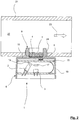
- a device 1 comprises a light source 2, a light receiver 3 and a sensor unit 4 . Furthermore, the device 1 has a temperature measuring means 5 , by means of which the temperature of the sensor unit 4 can be detected.
- the device 1 is constructed such that all electronic components are arranged within a housing 6 .
- This housing 6 is characterized in that it is fluidly completed by the respective medium to be examined, that is, an interior of the housing 6 is shielded by means of a wall 10 of the medium.
- the interior is separated by means of a partition wall 25 directly from a medium side of the housing 6 , wherein the sensor unit 4 is arranged on the medium side of the partition wall 25 .
- the walls 10 of the housing 6, in particular the partition wall 25, are formed here transparent.
- the light source 2, the light receiver 3 and the temperature measuring means 5 are arranged within the housing 6 .
- the optical sensor unit 4 is arranged outside the housing 6 , so that a direct exchange of at least individual particles of the analyte between the medium and the sensor unit 4 is possible.
- the sensor unit 4 is directly on an outer surface 12 of the partition 25 of the housing. 6 applied. It is formed here by a luminescent ink layer, which is arranged on an associated carrier.
- the temperature measuring means 5 is arranged directly on an opposite inner surface 13 of the partition wall 25 , so that a distance 14 between the sensor unit 4 and the temperature measuring means 5 is minimal. This has the advantage that a change in the temperature of the sensor unit 4 can be forwarded to the temperature measuring means 5 as quickly as possible so that the temperature measured by the temperature measuring means 5 at least substantially coincides with the actual temperature of the sensor unit 4 .
- the partition wall 25 has a heat transfer coefficient of about 100 W / m 2 K.
- the temperature measuring means 5 is formed here by an integrated temperature sensor, which is arranged on a printed circuit board 15 .
- This printed circuit board 15 is arranged in the immediate vicinity of the upper partition 25 of the housing 6 . It is further connected by means of a connecting line 20 with another circuit board 15 , which holds both the light source 2 and the light receiver 3 . By means of the connecting line 20 , an electrical connection between the circuit boards 15 is created.
- the light source 2 is formed in the example shown by a red LED. By means of the light source 2 , light is emitted in the direction of the optical sensor unit 4 . This light is in FIG. 1 illustrated by the arrow 19 shown there. In order to get to the optical sensor unit 4 , the light emitted from the light source 2 must pass through an excitation filter 16 which is suitable for transmitting only those wavelengths of the radiated light which are required for the excitation of the sensor unit 4 . In order for the light to strike the sensor unit 4 , it is understood that the housing 6 must be designed to be transparent at least in the region cooperating with the sensor unit 4 so that the light emitted by the light source 2 can strike the sensor unit 4 . In particular, the housing 6 may be formed entirely by a transparent plastic.
- the sensor unit 4 As a result of the excitation of the sensor unit 4 by means of the light emitted by the light source 2, the sensor unit 4 in turn emits light, with properties of the light thus emitted by the sensor unit 4 being directly related to the luminescent properties of the sensor unit 4 , the luminescence again being dependent on the concentration of the analyte on or in the sensor unit 4 depends.
- the light emitted by the sensor unit 4 is then received by the light receiver 3 .
- the light is in FIG. 1 symbolically illustrated by the arrow 18 shown there.
- the light receiver 3 is still preceded by an outlet filter 17 , only those Wavelengths of emitted from the sensor unit 4 light passes allowed to examine the concentration of the analyte.
- the luminescent properties of the sensor unit 4 are also very much dependent on the temperature of the sensor unit 4 in addition to the concentration of the respective analyte. For this reason, it is only necessary to constantly monitor the temperature of the sensor unit 4 by means of the temperature measuring means 5 .
- a thermal insulating layer 7 is arranged on a side of the sensor unit 4 facing away from the housing 6 . This has the primary technical effect that the sensor unit 4 is thermally isolated from the medium to be examined, so that a change in the temperature of the medium at least not directly, preferably not at all, affects the temperature of the sensor unit 4 .
- the significant advantage is achieved that the change in the temperature of the sensor unit 4 over time can be limited to a minimum and thus eliminate temperature fluctuations of the sensor unit 4 as the cause of possible measurement errors.
- the temperature measuring means 5 used can be made relatively simple, since in particular sudden changes in the temperature of the sensor unit 4 are not to be feared by significant amounts.
- the thermal insulation layer 7 here has a thickness 8 of about 2 mm.
- the support of the optical sensor unit 4 has a thickness of about 0.1 mm.
- the luminescent ink layer of the sensor unit 4 as such has only a thickness of about 0.01 mm.
- the heat transfer coefficient of the insulating layer 7 is here 30 W / m 2 K.
- the ratio of the heat transfer coefficient of the insulating layer 7 and the housing 6 (or the partition wall 25 ) here 0.3: 1.
- the thermal insulation layer 7 is formed in the example shown by sintered polytetrafluoroethylene.
- the insulating layer 7 has a multiplicity of very small pores which, in particular, allow the diffusion of the analyte proceeding from an upper side of the insulating layer 7 facing away from the housing 6 to a lower side of the insulating layer 7 facing the housing 6 .
- the pores of the insulating layer 7 here have a size of about 30 microns.
- the insulating layer 7 is arranged on the device 1 such that a direct contact between the medium to be examined and the sensor unit 4 is prevented.
- the device 1 has a measuring channel 9, which extends from the housing 6.
- the sensor unit 4 is arranged at a lower, the housing 6 facing the end of the measuring channel 9 and the insulating layer 7, so to speak "placed over it".
- the sensor unit 7 is positioned so that its underside is in direct contact with a surface of the sensor unit 4 facing away from the housing 6 . In other words, there is no free layer, for example an air layer, between the mutually facing surfaces of the insulating layer 7 and the sensor unit 4 .
- polytetrafluoroethylene is particularly advantageous in this respect insofar as it has hydrophobic properties which prevent the formation of a liquid film on the upper side of the insulating layer 7 . This ensures that the pores of the insulating layer 7, through which the respective analyte must migrate to the sensor unit 4 , are not sealed by means of a precipitated liquid.
- the adhesive by means of which, in the example shown, the same is connected to the inner circumferential surface 11 of the measuring channel 9 is also hydrophobic.
- the measuring channel 9 comprises on an outer circumferential surface an external thread 24, which cooperates with a complementary internal thread of a media line 21 .
- a respective medium 22 to be examined for example breathing air
- the medium 22 flows directly along the device 1 , wherein a direct exchange of a respective analyte between the medium 22 and the sensor unit 4 through the insulating layer 7 is possible therethrough.
- concentration of oxygen in the medium 22 should be investigated.
- the illustration readily shows that the medium 22 is at least thermally decoupled from the sensor unit 4 by means of the insulating layer 7 , so that any temperature fluctuations of the medium 22 have no direct effect on the temperature of the sensor unit 4 .
- the porosity of the insulating layer 7 allows a particularly rapid diffusion of the individual particles of the analyte to be examined through the insulating layer 7 , so that the concentration of the respective analyte in or on the sensor unit 4 within a very short time, in particular within less than two seconds. adapted to the concentration of the analyte in the medium 22 .
- the insulating layer 7 according to the invention for a particularly short response time of the sensor unit 4 is not a hindrance.
Landscapes
- Chemical & Material Sciences (AREA)
- Health & Medical Sciences (AREA)
- Life Sciences & Earth Sciences (AREA)
- Physics & Mathematics (AREA)
- Engineering & Computer Science (AREA)
- Analytical Chemistry (AREA)
- Immunology (AREA)
- Pathology (AREA)
- General Physics & Mathematics (AREA)
- Biochemistry (AREA)
- General Health & Medical Sciences (AREA)
- Combustion & Propulsion (AREA)
- Medicinal Chemistry (AREA)
- Food Science & Technology (AREA)
- Chemical Kinetics & Catalysis (AREA)
- Plasma & Fusion (AREA)
- Nuclear Medicine, Radiotherapy & Molecular Imaging (AREA)
- Investigating, Analyzing Materials By Fluorescence Or Luminescence (AREA)
- Investigating Or Analysing Materials By Optical Means (AREA)
Applications Claiming Priority (1)
| Application Number | Priority Date | Filing Date | Title |
|---|---|---|---|
| DE102016114918.7A DE102016114918B3 (de) | 2016-08-11 | 2016-08-11 | Vorrichtung zur Ermittlung der Konzentration eines Analyten in einem gasförmigen Medium |
Publications (3)
| Publication Number | Publication Date |
|---|---|
| EP3282244A1 true EP3282244A1 (fr) | 2018-02-14 |
| EP3282244C0 EP3282244C0 (fr) | 2023-07-26 |
| EP3282244B1 EP3282244B1 (fr) | 2023-07-26 |
Family
ID=59416552
Family Applications (1)
| Application Number | Title | Priority Date | Filing Date |
|---|---|---|---|
| EP17183201.7A Active EP3282244B1 (fr) | 2016-08-11 | 2017-07-26 | Dispositif de détermination de la concentration d'un analyte dans un milieu gazeux |
Country Status (3)
| Country | Link |
|---|---|
| US (1) | US10495619B2 (fr) |
| EP (1) | EP3282244B1 (fr) |
| DE (1) | DE102016114918B3 (fr) |
Families Citing this family (2)
| Publication number | Priority date | Publication date | Assignee | Title |
|---|---|---|---|---|
| JP6709429B2 (ja) * | 2015-12-21 | 2020-06-17 | スタンレー電気株式会社 | 水素濃度測定装置 |
| WO2024020073A1 (fr) | 2022-07-21 | 2024-01-25 | Conmed Corporation | Système et procédé de régulation de la concentration de gaz d'insufflation à l'aide d'un capteur optique d'oxygène |
Citations (6)
| Publication number | Priority date | Publication date | Assignee | Title |
|---|---|---|---|---|
| WO2002061399A1 (fr) * | 2001-01-31 | 2002-08-08 | Grouptek, Inc. | Appareil et procede de controle d'un analyte |
| US20070212792A1 (en) * | 2006-03-13 | 2007-09-13 | Cryovac, Inc. | Method and apparatus for measuring oxygen concentration |
| JP2008107091A (ja) * | 2006-10-23 | 2008-05-08 | Nippon Telegr & Teleph Corp <Ntt> | ガス濃度測定器 |
| US20130145845A1 (en) * | 2010-08-19 | 2013-06-13 | Inficon Ab | Gas sensor housing |
| WO2013181679A1 (fr) * | 2012-06-06 | 2013-12-12 | Joanneum Research Forschungsgesellschaft Mbh | Capteur optochimique |
| WO2015143229A1 (fr) * | 2014-03-20 | 2015-09-24 | Entegris-Jetalon Solutions, Inc. | Système et procédé de détection et de signalisation d'une fin de vie de composant dans un capteur d'oxygène dissous |
Family Cites Families (14)
| Publication number | Priority date | Publication date | Assignee | Title |
|---|---|---|---|---|
| DE9321286U1 (de) * | 1993-10-26 | 1997-01-09 | Mannesmann AG, 40213 Düsseldorf | Sonde zur Messung von Druck- und Temperaturprofilen |
| DE19512111C2 (de) * | 1995-04-03 | 1999-01-07 | Ifm Electronic Gmbh | Wärmeübergangskontroll- und/oder -meßgerät |
| US5865942A (en) | 1996-02-14 | 1999-02-02 | Sinclair; Frank | Seam welder |
| DE19756170C2 (de) * | 1997-12-17 | 2001-06-13 | Lpkf Laser & Electronics Gmbh | Verfahren zum Messen von Sorbatgehalten in Substraten |
| EP1327864A1 (fr) * | 2002-01-10 | 2003-07-16 | Abb Research Ltd. | Capteur de débit massique piézoélectrique |
| DE102004033303A1 (de) | 2004-04-16 | 2005-11-03 | Endress + Hauser Conducta Gesellschaft für Mess- und Regeltechnik mbH + Co. KG | Vorrichtung zur Bestimmung und/oder Überwachung eines in einem fluiden Prozessmedium enthaltenen Analyten |
| ES2390987T3 (es) * | 2008-12-18 | 2012-11-20 | F. Hoffmann-La Roche Ag | Método para comprobar la calidad del acoplamiento térmico de una celda de medición |
| DE102010030075A1 (de) * | 2010-06-15 | 2011-12-15 | Robert Bosch Gmbh | Vorrichtung zur Erfassung einer Temperatur eines fluiden Mediums |
| CH704445A1 (de) * | 2011-02-02 | 2012-08-15 | Kistler Holding Ag | Drucksensor. |
| WO2014111779A1 (fr) * | 2013-01-16 | 2014-07-24 | Koninklijke Philips N.V. | Capteur pour la détermination de concentration de gaz |
| DE102014112972A1 (de) | 2013-09-12 | 2015-03-12 | Endress + Hauser Conducta Gesellschaft für Mess- und Regeltechnik mbH + Co. KG | Messmembran für einen optochemischen oder amperometrischen Sensor |
| DE202014100330U1 (de) * | 2014-01-27 | 2015-05-08 | Neumann & Co. Gmbh | Thermischer Durchflussmesser |
| US10895563B2 (en) * | 2014-02-26 | 2021-01-19 | Trace-Ability, Inc. | Palette-based systems for analyte characterization |
| JP6185151B2 (ja) * | 2014-04-03 | 2017-08-23 | 株式会社日立ハイテクノロジーズ | 分析装置 |
-
2016
- 2016-08-11 DE DE102016114918.7A patent/DE102016114918B3/de active Active
-
2017
- 2017-07-26 EP EP17183201.7A patent/EP3282244B1/fr active Active
- 2017-08-11 US US15/675,300 patent/US10495619B2/en active Active
Patent Citations (6)
| Publication number | Priority date | Publication date | Assignee | Title |
|---|---|---|---|---|
| WO2002061399A1 (fr) * | 2001-01-31 | 2002-08-08 | Grouptek, Inc. | Appareil et procede de controle d'un analyte |
| US20070212792A1 (en) * | 2006-03-13 | 2007-09-13 | Cryovac, Inc. | Method and apparatus for measuring oxygen concentration |
| JP2008107091A (ja) * | 2006-10-23 | 2008-05-08 | Nippon Telegr & Teleph Corp <Ntt> | ガス濃度測定器 |
| US20130145845A1 (en) * | 2010-08-19 | 2013-06-13 | Inficon Ab | Gas sensor housing |
| WO2013181679A1 (fr) * | 2012-06-06 | 2013-12-12 | Joanneum Research Forschungsgesellschaft Mbh | Capteur optochimique |
| WO2015143229A1 (fr) * | 2014-03-20 | 2015-09-24 | Entegris-Jetalon Solutions, Inc. | Système et procédé de détection et de signalisation d'une fin de vie de composant dans un capteur d'oxygène dissous |
Also Published As
| Publication number | Publication date |
|---|---|
| EP3282244C0 (fr) | 2023-07-26 |
| US10495619B2 (en) | 2019-12-03 |
| US20180045699A1 (en) | 2018-02-15 |
| DE102016114918B3 (de) | 2017-11-02 |
| EP3282244B1 (fr) | 2023-07-26 |
Similar Documents
| Publication | Publication Date | Title |
|---|---|---|
| DE3918994C1 (fr) | ||
| EP0855592B1 (fr) | Détecteur de gaz optoacoustique | |
| DE69811098T2 (de) | Optische gasdetektion | |
| WO2008000433A1 (fr) | Détecteur spectroscopique et procédé pour déterminer la présence de sang et de marqueurs biologiques dans des liquides | |
| WO1989007753A1 (fr) | Mesurage de la temperature par ultrasons et application en spectroscopie optique et en calorimetrie | |
| DE102016003452B4 (de) | Elektrochemischer Gassensor | |
| DE10058469C1 (de) | Optischer Gassensor | |
| AT512498A4 (de) | Opto-chemischer Sensor | |
| EP3282244B1 (fr) | Dispositif de détermination de la concentration d'un analyte dans un milieu gazeux | |
| DE102009014946B4 (de) | Verfahren und Vorrichtung zur Messung der Wasserspannung | |
| DE112013007716T5 (de) | Optischer Fasersensor zur Ölzustandsüberwachung | |
| DE102008048715A1 (de) | Verbesserung der Signalqualität von Feldeffekttransistoren aufweisenden Feuchtesensoren oder Gassensoren | |
| DE102014214026A1 (de) | Sensor zum Erfassen einer Flüssigkeit in einem Fluidkanal | |
| EP0981737B1 (fr) | Detecteur pour determiner la teneur en humidite | |
| EP3596447A1 (fr) | Dispositif pour la détection optique compensée en température d'une teneur en oxygène d'un fluide | |
| DE2710473A1 (de) | Schaltungsanordnung zur bestimmung der waermeverlustgeschwindigkeit | |
| DE10008969C2 (de) | Alkoholsensor und Betriebsverfahren | |
| DE112018004522T5 (de) | Chemischer Sensor und Verfahren zum Bilden desselben | |
| DE102022116825A1 (de) | Sensor-Anordnung mit einem elektrochemischen Sensor und einem Temperatur-Sensor und Verfahren unter Verwendung einer solchen Sensor-Anordnung | |
| DE10155131B4 (de) | Sensor bzw. Füllstandsmeßgerät sowie Schutzgehäuse für ein elektronisches Gerät bzw. einen Füllstandssensor | |
| DE102025107224A1 (de) | Analysegerät mit einem chemischen Filter um die Messkammer | |
| DE102013207629A1 (de) | Optischer Sensor | |
| DE102008006035B3 (de) | Mikrotechnisches Bauelement zur Untersuchung einer fluidischen Probe und ein Verfahren zu dessen Herstellung | |
| DE102023204890A1 (de) | Ergospirometrievorrichtung und entsprechendes Herstellungsverfahren | |
| AT14051U1 (de) | Optochemischer Sensor |
Legal Events
| Date | Code | Title | Description |
|---|---|---|---|
| PUAI | Public reference made under article 153(3) epc to a published international application that has entered the european phase |
Free format text: ORIGINAL CODE: 0009012 |
|
| STAA | Information on the status of an ep patent application or granted ep patent |
Free format text: STATUS: THE APPLICATION HAS BEEN PUBLISHED |
|
| AK | Designated contracting states |
Kind code of ref document: A1 Designated state(s): AL AT BE BG CH CY CZ DE DK EE ES FI FR GB GR HR HU IE IS IT LI LT LU LV MC MK MT NL NO PL PT RO RS SE SI SK SM TR |
|
| AX | Request for extension of the european patent |
Extension state: BA ME |
|
| STAA | Information on the status of an ep patent application or granted ep patent |
Free format text: STATUS: REQUEST FOR EXAMINATION WAS MADE |
|
| 17P | Request for examination filed |
Effective date: 20180723 |
|
| RBV | Designated contracting states (corrected) |
Designated state(s): AL AT BE BG CH CY CZ DE DK EE ES FI FR GB GR HR HU IE IS IT LI LT LU LV MC MK MT NL NO PL PT RO RS SE SI SK SM TR |
|
| STAA | Information on the status of an ep patent application or granted ep patent |
Free format text: STATUS: EXAMINATION IS IN PROGRESS |
|
| 17Q | First examination report despatched |
Effective date: 20210408 |
|
| GRAP | Despatch of communication of intention to grant a patent |
Free format text: ORIGINAL CODE: EPIDOSNIGR1 |
|
| STAA | Information on the status of an ep patent application or granted ep patent |
Free format text: STATUS: GRANT OF PATENT IS INTENDED |
|
| RIC1 | Information provided on ipc code assigned before grant |
Ipc: G01N 21/77 20060101ALN20230131BHEP Ipc: G01N 21/64 20060101ALN20230131BHEP Ipc: G01N 33/00 20060101ALI20230131BHEP Ipc: G01N 21/78 20060101AFI20230131BHEP |
|
| RIC1 | Information provided on ipc code assigned before grant |
Ipc: G01N 21/77 20060101ALN20230208BHEP Ipc: G01N 21/64 20060101ALN20230208BHEP Ipc: G01N 33/00 20060101ALI20230208BHEP Ipc: G01N 21/78 20060101AFI20230208BHEP |
|
| INTG | Intention to grant announced |
Effective date: 20230223 |
|
| RIC1 | Information provided on ipc code assigned before grant |
Ipc: G01N 21/77 20060101ALN20230215BHEP Ipc: G01N 21/64 20060101ALN20230215BHEP Ipc: G01N 33/00 20060101ALI20230215BHEP Ipc: G01N 21/78 20060101AFI20230215BHEP |
|
| GRAS | Grant fee paid |
Free format text: ORIGINAL CODE: EPIDOSNIGR3 |
|
| GRAA | (expected) grant |
Free format text: ORIGINAL CODE: 0009210 |
|
| STAA | Information on the status of an ep patent application or granted ep patent |
Free format text: STATUS: THE PATENT HAS BEEN GRANTED |
|
| APBM | Appeal reference recorded |
Free format text: ORIGINAL CODE: EPIDOSNREFNO |
|
| PUAC | Information related to the publication of a b1 document modified or deleted |
Free format text: ORIGINAL CODE: 0009299EPPU |
|
| STAA | Information on the status of an ep patent application or granted ep patent |
Free format text: STATUS: GRANT OF PATENT IS INTENDED |
|
| AK | Designated contracting states |
Kind code of ref document: B1 Designated state(s): AL AT BE BG CH CY CZ DE DK EE ES FI FR GB GR HR HU IE IS IT LI LT LU LV MC MK MT NL NO PL PT RO RS SE SI SK SM TR |
|
| REG | Reference to a national code |
Ref country code: CH Ref legal event code: PK Free format text: DIE ERTEILUNG WURDE VOM EPA WIDERRUFEN. Ref country code: GB Ref legal event code: FG4D Free format text: NOT ENGLISH Ref country code: CH Ref legal event code: EP |
|
| REG | Reference to a national code |
Ref country code: DE Ref legal event code: R096 Ref document number: 502017014755 Country of ref document: DE |
|
| APAF | Appeal reference modified |
Free format text: ORIGINAL CODE: EPIDOSCREFNE |
|
| REG | Reference to a national code |
Ref country code: AT Ref legal event code: REF Ref document number: 1571203 Country of ref document: AT Kind code of ref document: T Effective date: 20230615 |
|
| REG | Reference to a national code |
Ref country code: IE Ref legal event code: FG4D Free format text: LANGUAGE OF EP DOCUMENT: GERMAN |
|
| GRAA | (expected) grant |
Free format text: ORIGINAL CODE: 0009210 |
|
| STAA | Information on the status of an ep patent application or granted ep patent |
Free format text: STATUS: THE PATENT HAS BEEN GRANTED |
|
| DB1 | Publication of patent cancelled |
Effective date: 20230526 |
|
| REG | Reference to a national code |
Ref country code: DE Ref legal event code: R107 Ref document number: 502017014755 Country of ref document: DE |
|
| AK | Designated contracting states |
Kind code of ref document: B1 Designated state(s): AL AT BE BG CH CY CZ DE DK EE ES FI FR GB GR HR HU IE IS IT LI LT LU LV MC MK MT NL NO PL PT RO RS SE SI SK SM TR |
|
| REG | Reference to a national code |
Ref country code: CH Ref legal event code: EP |
|
| REG | Reference to a national code |
Ref country code: DE Ref legal event code: R096 Ref document number: 502017014755 Country of ref document: DE |
|
| U01 | Request for unitary effect filed |
Effective date: 20230810 |
|
| U07 | Unitary effect registered |
Designated state(s): AT BE BG DE DK EE FI FR IT LT LU LV MT NL PT SE SI Effective date: 20230829 |
|
| U20 | Renewal fee for the european patent with unitary effect paid |
Year of fee payment: 7 Effective date: 20230829 |
|
| RAP4 | Party data changed (patent owner data changed or rights of a patent transferred) |
Owner name: PYROSCIENCE GMBH |
|
| U1H | Name or address of the proprietor changed after the registration of the unitary effect |
Owner name: PYROSCIENCE GMBH; DE |
|
| PG25 | Lapsed in a contracting state [announced via postgrant information from national office to epo] |
Ref country code: NO Free format text: LAPSE BECAUSE OF FAILURE TO SUBMIT A TRANSLATION OF THE DESCRIPTION OR TO PAY THE FEE WITHIN THE PRESCRIBED TIME-LIMIT Effective date: 20230831 |
|
| REG | Reference to a national code |
Ref country code: LT Ref legal event code: MG9D |
|
| PG25 | Lapsed in a contracting state [announced via postgrant information from national office to epo] |
Ref country code: IS Free format text: LAPSE BECAUSE OF FAILURE TO SUBMIT A TRANSLATION OF THE DESCRIPTION OR TO PAY THE FEE WITHIN THE PRESCRIBED TIME-LIMIT Effective date: 20230930 |
|
| PG25 | Lapsed in a contracting state [announced via postgrant information from national office to epo] |
Ref country code: GR Free format text: LAPSE BECAUSE OF FAILURE TO SUBMIT A TRANSLATION OF THE DESCRIPTION OR TO PAY THE FEE WITHIN THE PRESCRIBED TIME-LIMIT Effective date: 20231027 |
|
| PG25 | Lapsed in a contracting state [announced via postgrant information from national office to epo] |
Ref country code: RS Free format text: LAPSE BECAUSE OF FAILURE TO SUBMIT A TRANSLATION OF THE DESCRIPTION OR TO PAY THE FEE WITHIN THE PRESCRIBED TIME-LIMIT Effective date: 20230726 Ref country code: NO Free format text: LAPSE BECAUSE OF FAILURE TO SUBMIT A TRANSLATION OF THE DESCRIPTION OR TO PAY THE FEE WITHIN THE PRESCRIBED TIME-LIMIT Effective date: 20231026 Ref country code: HR Free format text: LAPSE BECAUSE OF FAILURE TO SUBMIT A TRANSLATION OF THE DESCRIPTION OR TO PAY THE FEE WITHIN THE PRESCRIBED TIME-LIMIT Effective date: 20230726 Ref country code: GR Free format text: LAPSE BECAUSE OF FAILURE TO SUBMIT A TRANSLATION OF THE DESCRIPTION OR TO PAY THE FEE WITHIN THE PRESCRIBED TIME-LIMIT Effective date: 20231027 |
|
| REG | Reference to a national code |
Ref country code: CH Ref legal event code: PL |
|
| REG | Reference to a national code |
Ref country code: IE Ref legal event code: MM4A |
|
| PG25 | Lapsed in a contracting state [announced via postgrant information from national office to epo] |
Ref country code: ES Free format text: LAPSE BECAUSE OF FAILURE TO SUBMIT A TRANSLATION OF THE DESCRIPTION OR TO PAY THE FEE WITHIN THE PRESCRIBED TIME-LIMIT Effective date: 20230726 |
|
| REG | Reference to a national code |
Ref country code: DE Ref legal event code: R097 Ref document number: 502017014755 Country of ref document: DE |
|
| PG25 | Lapsed in a contracting state [announced via postgrant information from national office to epo] |
Ref country code: SM Free format text: LAPSE BECAUSE OF FAILURE TO SUBMIT A TRANSLATION OF THE DESCRIPTION OR TO PAY THE FEE WITHIN THE PRESCRIBED TIME-LIMIT Effective date: 20230726 Ref country code: RO Free format text: LAPSE BECAUSE OF FAILURE TO SUBMIT A TRANSLATION OF THE DESCRIPTION OR TO PAY THE FEE WITHIN THE PRESCRIBED TIME-LIMIT Effective date: 20230726 Ref country code: ES Free format text: LAPSE BECAUSE OF FAILURE TO SUBMIT A TRANSLATION OF THE DESCRIPTION OR TO PAY THE FEE WITHIN THE PRESCRIBED TIME-LIMIT Effective date: 20230726 Ref country code: CZ Free format text: LAPSE BECAUSE OF FAILURE TO SUBMIT A TRANSLATION OF THE DESCRIPTION OR TO PAY THE FEE WITHIN THE PRESCRIBED TIME-LIMIT Effective date: 20230726 Ref country code: MC Free format text: LAPSE BECAUSE OF FAILURE TO SUBMIT A TRANSLATION OF THE DESCRIPTION OR TO PAY THE FEE WITHIN THE PRESCRIBED TIME-LIMIT Effective date: 20230726 Ref country code: CH Free format text: LAPSE BECAUSE OF NON-PAYMENT OF DUE FEES Effective date: 20230731 Ref country code: SK Free format text: LAPSE BECAUSE OF FAILURE TO SUBMIT A TRANSLATION OF THE DESCRIPTION OR TO PAY THE FEE WITHIN THE PRESCRIBED TIME-LIMIT Effective date: 20230726 |
|
| PLBE | No opposition filed within time limit |
Free format text: ORIGINAL CODE: 0009261 |
|
| STAA | Information on the status of an ep patent application or granted ep patent |
Free format text: STATUS: NO OPPOSITION FILED WITHIN TIME LIMIT |
|
| 26N | No opposition filed |
Effective date: 20240429 |
|
| U20 | Renewal fee for the european patent with unitary effect paid |
Year of fee payment: 8 Effective date: 20240529 |
|
| PG25 | Lapsed in a contracting state [announced via postgrant information from national office to epo] |
Ref country code: IE Free format text: LAPSE BECAUSE OF NON-PAYMENT OF DUE FEES Effective date: 20230726 |
|
| PG25 | Lapsed in a contracting state [announced via postgrant information from national office to epo] |
Ref country code: IE Free format text: LAPSE BECAUSE OF NON-PAYMENT OF DUE FEES Effective date: 20230726 |
|
| U20 | Renewal fee for the european patent with unitary effect paid |
Year of fee payment: 9 Effective date: 20250502 |
|
| PG25 | Lapsed in a contracting state [announced via postgrant information from national office to epo] |
Ref country code: PL Free format text: LAPSE BECAUSE OF FAILURE TO SUBMIT A TRANSLATION OF THE DESCRIPTION OR TO PAY THE FEE WITHIN THE PRESCRIBED TIME-LIMIT Effective date: 20230726 |
|
| PG25 | Lapsed in a contracting state [announced via postgrant information from national office to epo] |
Ref country code: CY Free format text: LAPSE BECAUSE OF FAILURE TO SUBMIT A TRANSLATION OF THE DESCRIPTION OR TO PAY THE FEE WITHIN THE PRESCRIBED TIME-LIMIT; INVALID AB INITIO Effective date: 20170726 |
|
| U1N | Appointed representative for the unitary patent procedure changed after the registration of the unitary effect |
Representative=s name: PELLENGAHR, MAXIMILIAN RUDOLF; DE |
|
| PG25 | Lapsed in a contracting state [announced via postgrant information from national office to epo] |
Ref country code: HU Free format text: LAPSE BECAUSE OF FAILURE TO SUBMIT A TRANSLATION OF THE DESCRIPTION OR TO PAY THE FEE WITHIN THE PRESCRIBED TIME-LIMIT; INVALID AB INITIO Effective date: 20170726 |
|
| PG25 | Lapsed in a contracting state [announced via postgrant information from national office to epo] |
Ref country code: TR Free format text: LAPSE BECAUSE OF FAILURE TO SUBMIT A TRANSLATION OF THE DESCRIPTION OR TO PAY THE FEE WITHIN THE PRESCRIBED TIME-LIMIT Effective date: 20230726 |