EP3282490A1 - Interconnecteur et panneau solaire - Google Patents
Interconnecteur et panneau solaire Download PDFInfo
- Publication number
- EP3282490A1 EP3282490A1 EP17184886.4A EP17184886A EP3282490A1 EP 3282490 A1 EP3282490 A1 EP 3282490A1 EP 17184886 A EP17184886 A EP 17184886A EP 3282490 A1 EP3282490 A1 EP 3282490A1
- Authority
- EP
- European Patent Office
- Prior art keywords
- detour
- photovoltaic cell
- electrode
- interconnector
- solar panel
- Prior art date
- Legal status (The legal status is an assumption and is not a legal conclusion. Google has not performed a legal analysis and makes no representation as to the accuracy of the status listed.)
- Granted
Links
Images



Classifications
-
- H—ELECTRICITY
- H10—SEMICONDUCTOR DEVICES; ELECTRIC SOLID-STATE DEVICES NOT OTHERWISE PROVIDED FOR
- H10F—INORGANIC SEMICONDUCTOR DEVICES SENSITIVE TO INFRARED RADIATION, LIGHT, ELECTROMAGNETIC RADIATION OF SHORTER WAVELENGTH OR CORPUSCULAR RADIATION
- H10F19/00—Integrated devices, or assemblies of multiple devices, comprising at least one photovoltaic cell covered by group H10F10/00, e.g. photovoltaic modules
- H10F19/90—Structures for connecting between photovoltaic cells, e.g. interconnections or insulating spacers
- H10F19/902—Structures for connecting between photovoltaic cells, e.g. interconnections or insulating spacers for series or parallel connection of photovoltaic cells
- H10F19/904—Structures for connecting between photovoltaic cells, e.g. interconnections or insulating spacers for series or parallel connection of photovoltaic cells characterised by the shapes of the structures
-
- H—ELECTRICITY
- H10—SEMICONDUCTOR DEVICES; ELECTRIC SOLID-STATE DEVICES NOT OTHERWISE PROVIDED FOR
- H10F—INORGANIC SEMICONDUCTOR DEVICES SENSITIVE TO INFRARED RADIATION, LIGHT, ELECTROMAGNETIC RADIATION OF SHORTER WAVELENGTH OR CORPUSCULAR RADIATION
- H10F19/00—Integrated devices, or assemblies of multiple devices, comprising at least one photovoltaic cell covered by group H10F10/00, e.g. photovoltaic modules
- H10F19/80—Encapsulations or containers for integrated devices, or assemblies of multiple devices, having photovoltaic cells
-
- H—ELECTRICITY
- H10—SEMICONDUCTOR DEVICES; ELECTRIC SOLID-STATE DEVICES NOT OTHERWISE PROVIDED FOR
- H10F—INORGANIC SEMICONDUCTOR DEVICES SENSITIVE TO INFRARED RADIATION, LIGHT, ELECTROMAGNETIC RADIATION OF SHORTER WAVELENGTH OR CORPUSCULAR RADIATION
- H10F19/00—Integrated devices, or assemblies of multiple devices, comprising at least one photovoltaic cell covered by group H10F10/00, e.g. photovoltaic modules
- H10F19/80—Encapsulations or containers for integrated devices, or assemblies of multiple devices, having photovoltaic cells
- H10F19/807—Double-glass encapsulation, e.g. photovoltaic cells arranged between front and rear glass sheets
-
- H—ELECTRICITY
- H10—SEMICONDUCTOR DEVICES; ELECTRIC SOLID-STATE DEVICES NOT OTHERWISE PROVIDED FOR
- H10F—INORGANIC SEMICONDUCTOR DEVICES SENSITIVE TO INFRARED RADIATION, LIGHT, ELECTROMAGNETIC RADIATION OF SHORTER WAVELENGTH OR CORPUSCULAR RADIATION
- H10F19/00—Integrated devices, or assemblies of multiple devices, comprising at least one photovoltaic cell covered by group H10F10/00, e.g. photovoltaic modules
- H10F19/80—Encapsulations or containers for integrated devices, or assemblies of multiple devices, having photovoltaic cells
- H10F19/85—Protective back sheets
-
- H—ELECTRICITY
- H10—SEMICONDUCTOR DEVICES; ELECTRIC SOLID-STATE DEVICES NOT OTHERWISE PROVIDED FOR
- H10F—INORGANIC SEMICONDUCTOR DEVICES SENSITIVE TO INFRARED RADIATION, LIGHT, ELECTROMAGNETIC RADIATION OF SHORTER WAVELENGTH OR CORPUSCULAR RADIATION
- H10F19/00—Integrated devices, or assemblies of multiple devices, comprising at least one photovoltaic cell covered by group H10F10/00, e.g. photovoltaic modules
- H10F19/90—Structures for connecting between photovoltaic cells, e.g. interconnections or insulating spacers
- H10F19/902—Structures for connecting between photovoltaic cells, e.g. interconnections or insulating spacers for series or parallel connection of photovoltaic cells
-
- H—ELECTRICITY
- H10—SEMICONDUCTOR DEVICES; ELECTRIC SOLID-STATE DEVICES NOT OTHERWISE PROVIDED FOR
- H10F—INORGANIC SEMICONDUCTOR DEVICES SENSITIVE TO INFRARED RADIATION, LIGHT, ELECTROMAGNETIC RADIATION OF SHORTER WAVELENGTH OR CORPUSCULAR RADIATION
- H10F19/00—Integrated devices, or assemblies of multiple devices, comprising at least one photovoltaic cell covered by group H10F10/00, e.g. photovoltaic modules
- H10F19/90—Structures for connecting between photovoltaic cells, e.g. interconnections or insulating spacers
- H10F19/902—Structures for connecting between photovoltaic cells, e.g. interconnections or insulating spacers for series or parallel connection of photovoltaic cells
- H10F19/906—Structures for connecting between photovoltaic cells, e.g. interconnections or insulating spacers for series or parallel connection of photovoltaic cells characterised by the materials of the structures
-
- H—ELECTRICITY
- H10—SEMICONDUCTOR DEVICES; ELECTRIC SOLID-STATE DEVICES NOT OTHERWISE PROVIDED FOR
- H10F—INORGANIC SEMICONDUCTOR DEVICES SENSITIVE TO INFRARED RADIATION, LIGHT, ELECTROMAGNETIC RADIATION OF SHORTER WAVELENGTH OR CORPUSCULAR RADIATION
- H10F19/00—Integrated devices, or assemblies of multiple devices, comprising at least one photovoltaic cell covered by group H10F10/00, e.g. photovoltaic modules
- H10F19/90—Structures for connecting between photovoltaic cells, e.g. interconnections or insulating spacers
- H10F19/902—Structures for connecting between photovoltaic cells, e.g. interconnections or insulating spacers for series or parallel connection of photovoltaic cells
- H10F19/908—Structures for connecting between photovoltaic cells, e.g. interconnections or insulating spacers for series or parallel connection of photovoltaic cells for back-contact photovoltaic cells
-
- Y—GENERAL TAGGING OF NEW TECHNOLOGICAL DEVELOPMENTS; GENERAL TAGGING OF CROSS-SECTIONAL TECHNOLOGIES SPANNING OVER SEVERAL SECTIONS OF THE IPC; TECHNICAL SUBJECTS COVERED BY FORMER USPC CROSS-REFERENCE ART COLLECTIONS [XRACs] AND DIGESTS
- Y02—TECHNOLOGIES OR APPLICATIONS FOR MITIGATION OR ADAPTATION AGAINST CLIMATE CHANGE
- Y02E—REDUCTION OF GREENHOUSE GAS [GHG] EMISSIONS, RELATED TO ENERGY GENERATION, TRANSMISSION OR DISTRIBUTION
- Y02E10/00—Energy generation through renewable energy sources
- Y02E10/50—Photovoltaic [PV] energy
Definitions
- the present invention relates to an interconnector and a solar panel.
- Japanese Laid-Open Patent Publication No. 2005-191479 discloses a prior art solar panel.
- the solar panel includes a protection cover, a back cover, a first photovoltaic cell, a second photovoltaic cell, an interconnector, and an encapsulation member.
- the protection cover is formed by an inorganic glass and transparent from an upper surface to a lower surface of the protection cover.
- the back cover is formed by a resin film or the like.
- the first photovoltaic cell and the second photovoltaic cell are located adjacent to each other in a first direction. More specifically, the first photovoltaic cell is located at one side in the first direction. The second photovoltaic cell is located at the other side in the first direction.
- the interconnector is flat.
- the interconnector is located between the first photovoltaic cell and the second photovoltaic cell to be parallel to the first photovoltaic cell and the second photovoltaic cell.
- the interconnector includes a first electrode connected to the first photovoltaic cell, a second electrode connected to the second photovoltaic cell, and a joint that connects the first electrode and the second electrode.
- the first photovoltaic cell, the second photovoltaic cell, and the interconnector, which are located between the protection cover and the back cover, are encapsulated and fixed to one another by the encapsulation member.
- the first photovoltaic cell and the second photovoltaic cell which are adjacent to each other in the first direction, are electrically connected to each other by the interconnector.
- This type of solar panel may be expanded and contracted by changes in the temperature that occur when the solar panel is manufactured or used. This changes the interval between the first photovoltaic cell and the second photovoltaic cell, which are adjacent to each other. Therefore, when the interval of the first photovoltaic cell and the second photovoltaic cell is narrowed by the contraction of the solar panel caused by changes in the temperature, the first photovoltaic cell and the second photovoltaic cell apply a compression load to the interconnector. More specifically, the interconnector is pressed by the first photovoltaic cell and the second photovoltaic cell from opposite sides. Such a load may break the interconnector in a thickness-wise direction.
- the first photovoltaic cell and the second photovoltaic cell apply a tension load to the interconnector. More specifically, the interconnector is pulled by the first photovoltaic cell and the second photovoltaic cell from opposite sides. This may separate the first electrode from the first photovoltaic cell or the second electrode from the second photovoltaic cell.
- the first photovoltaic cell and the second photovoltaic cell may be electrically disconnected from each other.
- the protection cover and the back cover are formed from a resin, the protection cover and the back cover each have a large thermal expansion coefficient. Thus, the above problem becomes more prominent.
- an interconnector is configured to electrically connect a first photovoltaic cell and a second photovoltaic cell that are adjacent to each other in a first direction.
- the first photovoltaic cell is located at a first side in the first direction.
- the second photovoltaic cell is located at a second side in the first direction.
- the interconnector includes a first electrode configured to be connected to the first photovoltaic cell, a second electrode configured to be connected to the second photovoltaic cell, and a connection body that connects the first electrode and the second electrode.
- the connection body includes a first detour connected to the first electrode and extended toward a first side in a second direction that is orthogonal to the first direction, a second detour connected to the second electrode and extended toward the first side in the second direction, and a joint extended in the first direction to connect the first detour and the second detour.
- the first detour includes a first curved part that is curved toward the first side in the first direction and connected to the first electrode.
- a solar panel includes the interconnector; the first photovoltaic cell; the second photovoltaic cell; a protection cover including an upper surface and a lower surface and is transparent from the upper surface to the lower surface; a back cover that cooperates with the protection cover to cover the first photovoltaic cell, the second photovoltaic cell, and the interconnector, which are located between the protection cover and the back cover; and an encapsulation member that encapsulates the first photovoltaic cell, the second photovoltaic cell, and the interconnector and fixes the first photovoltaic cell, the second photovoltaic cell, and the interconnector to one another.
- a first embodiment of a solar panel includes a protection plate 1, a plurality of first photovoltaic cells 3, a plurality of second photovoltaic cells 5, a plurality of tab wires 7a, 7b, a plurality of interconnectors 9, and an encapsulation member 11.
- the solar panel further includes a back panel 13.
- the protection plate 1 corresponds to a protection cover.
- the back panel 13 corresponds to a back cover. To simplify the illustration, Fig. 1 does not show a portion of the protection plate 1 that is indicated by a broken line.
- the directions indicated by arrows in Fig. 1 define a left-right direction and a front-rear direction of the solar panel.
- the left-right direction is orthogonal to the front-rear direction.
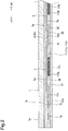
- the thickness-wise direction of the solar panel is defined as a vertical direction for example, referring to Fig. 2 .
- the left-right direction of the solar panel corresponds to a first direction. More specifically, the left side corresponds to a first side (one side) in the first direction.
- the right side corresponds to a second side (the other side) in the first direction.
- the front-rear direction of the solar panel corresponds to a second direction. More specifically, the rear side corresponds to a first side (one side) in the second direction.
- the front side corresponds to a second side (the other side) in the second direction.
- the protection plate 1 which includes an upper surface 1 a and a lower surface 1 b, is formed from a resin, the main component of which is polycarbonate, and transparent from the upper surface 1 a to the lower surface 1 b.
- the upper surface 1 a of the protection plate 1 defines an upper surface of the solar panel, that is, an ornamental surface of the solar panel.
- the upper surface 1 a is flat and level.
- the lower surface 1 b is also flat and parallel to the upper surface 1 a.
- the protection plate 1 is rectangular and flat.
- the protection plate 1 may be formed from, for example, another resin or an inorganic glass.
- the protection plate 1 may be designed to have an appropriate thickness.
- the protection cover may be formed, for example, by a transparent protection film instead of the protection plate 1.
- the protection plate 1 includes a shield 10.
- the shield 10 includes a body portion 10a, which is configured to shield the tab wires 7a, 7b from the side of the upper surface 1 a of the protection plate 1, and a plurality of connection portions 10b.
- the connection portions 10b are configured to shield the interconnectors 9 and first and second links 15a, 15b, which will be described later, from the side of the upper surface 1 a.
- the body portion 10a and the connection portions 10b are formed by painting predetermined positions of the lower surface 1 b of the protection plate 1 with an opaque color such as black or printing the predetermined positions of the lower surface 1 b in an opaque color such as black. More specifically, the body portion 10a is located on a position of the protection plate 1 defining an outer region of a photovoltaic cell group that includes the first photovoltaic cells 3 and the second photovoltaic cells 5. The body portion 10a is frame-shaped to surround the first and second photovoltaic cells 3, 5. Each of the connection portions 10b is located at an inner side of the body portion 10a and extended in the front-rear direction of the protection plate 1 to be continuous with a front end and rear end of the body portion 10a.
- the number of the connection portions 10b is set in accordance with the number of intervals between adjacent ones of the first photovoltaic cells 3 and the second photovoltaic cells 5 in the left-right direction.
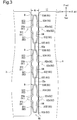
- the size of the connection portions 10b is set in correspondence with the size of the interval between the first photovoltaic cell 3 and the second photovoltaic cell 5 that are adjacent to each other in the left-right direction, more specifically, the size of an interval W (refer to Fig. 3 ), which will be described later.
- Figs. 2 and 6 to 8 do not show the shield 10.
- the first and second photovoltaic cells 3, 5 have the same structure and the same properties. More specifically, each of the first photovoltaic cells 3 has the form of a thin film and includes an upper surface 3a and a lower surface 3b. Also, each of the second photovoltaic cells 5 has the form of a thin film and includes an upper surface 5a and a lower surface 5b.
- the lower surfaces 3b of the first photovoltaic cells 3 and the lower surfaces 5b of the second photovoltaic cells 5 each include a conductive portion (not shown). Alternatively, the upper surfaces 3a of the first photovoltaic cells 3 and the upper surfaces 5a of the second photovoltaic cells 5 may each include a conductive portion.
- the first and second photovoltaic cells 3, 5 are arranged in a lattice in the front-rear and left-right directions of the solar panel. Additionally, the first photovoltaic cells 3 and the second photovoltaic cells 5 are alternately arranged adjacent to one another in the left-right direction. The size and number of the first and second photovoltaic cells 3, 5 may be changed in accordance with, for example, the size of the solar panel.
- the tab wires 7a, 7b are formed by thin metal plates.
- the tab wires 7a, 7b are located at the right end or left end of the solar panel.
- the tab wires 7a, 7b are arranged at fixed intervals.
- the tab wires 7a, 7b may electrically connect the first photovoltaic cells 3 that are located in different rows in the front-rear direction.
- the tab wires 7a, 7b may electrically connect the second photovoltaic cells 5 that are located in different rows in the front-rear direction.
- the positions where the tab wires 7a, 7b are connected to the first photovoltaic cells 3 and the positions where the tab wires 7a, 7b are connected to the second photovoltaic cells 5 may be changed in addition to the shape and number of the tab wires 7a, 7b.
- the three interconnectors 9 are connected by the first link 15a and the second link 15b to form an interconnector group 90.
- the interconnector group 90 that is, the three interconnectors 9 and the first and second links 15a, 15b, is integrally formed by stamping a copper plate.
- the interconnector group 90 is flat and parallel to the first photovoltaic cells 3 and the second photovoltaic cells 5 (refer to Fig. 2 ).
- a metal plate that differs from the copper plate may be used to form the interconnector group 90.
- the number of the interconnectors 9 forming the interconnector group 90 may be changed as long as the number is two or greater.
- the interconnector 9 includes a first electrode 91, a second electrode 92, and a connection body 93.
- the first electrode 91, the second electrode 92, and the connection body 93 are formed integrally with each other by stamping a copper plate as described above.
- the first electrode 91 is located at the left side of the interconnector 9.
- the second electrode 92 is located at the right side of the interconnector 9.
- the first electrode 91 includes a first base 91 a, which extends in the front-rear direction of the interconnector 9, and a first contact portion 91 b, which is integral with the first base 91 a and extended leftward from the first base 91 a.
- the second electrode 92 includes a second base 92a, which extends in the front-rear direction of the interconnector 9, and a second contact portion 92b, which is integral with the second base 92a and extended rightward from the second base 92a.
- the connection body 93 has the form of a fine line in a plan view.
- the connection body 93 includes a rear first detour 931, a rear second detour 932, a front first detour 933, a front second detour 934, a first joint 935, and a second joint 936.
- the rear first detour 931 and the rear second detour 932 are located at one side in the second direction.
- the front first detour 933 and the front second detour 934 are located at the other side in the second direction.
- the rear first detour 931 and the front first detour 933 are located at the left side of the connection body 93.
- the rear second detour 932 and the front second detour 934 are located at the right side of the connection body 93.
- the rear second detour 932 and the front second detour 934 are also separated from each other in the front-rear direction.
- the first joint 935 is located on a rear end of the connection body 93.
- the second joint 936 is located on a front end of the connection body 93.
- Each of the rear first detour 931 and the rear second detour 932 extends as a single line toward the rear of the interconnector 9.
- Each of the front first detour 933 and the front second detour 934 extends as a single line toward the front of the interconnector 9.
- the rear first detour 931 includes a rear first body part 931 a and a rear first curved part 931 b.
- the rear second detour 932 includes a rear second body part 932a and a rear second curved part 932b.
- the front first detour 933 includes a front first body part 933a and a front first curved part 933b.
- the front second detour 934 includes a front second body part 934a and a front second curved part 934b.
- the rear first curved part 931 b and the front first curved part 933b each correspond to a first curved part.
- the rear first detour 931 and the front first detour 933 are symmetrical at front and rear sides of the interconnector 9.
- the rear second detour 932 and the front second detour 934 are symmetrical at the front and rear sides.
- the structures of the rear first detour 931 and the rear second detour 932 will be described in detail.
- the structures of the front first detour 933 and the front second detour 934 will not be described in detail.
- the rear first body part 931 a linearly extends from the rear first curved part 931 b toward the rear of the interconnector 9 and then gradually toward the rear second detour 932.
- the rear first curved part 931 b is located on a side of the rear first detour 931 corresponding to the first electrode 91. More specifically, the rear first curved part 931 b corresponds to a front region of the rear first detour 931.
- Fig. 5 shows an enlarged view of a region X shown in Fig. 4 .
- the rear first curved part 931 b is, more specifically, a part of the rear first detour 931 defined by broken lines a1, b1 of Fig. 5 .
- the rear end of the rear first curved part 931 b is connected to the front end of the rear first body part 931 a.
- the rear first curved part 931 b is curved rightward from the front end of the rear first body part 931 a toward the rear second detour 932 and then toward the first electrode 91, more specifically, largely curved leftward, that is, toward a side opposite to the second electrode 92.
- the rear first curved part 931 b is curved to bulge toward the rear second curved part 932b.
- the front end of the rear first curved part 931 b is connected to a rear end region of the first base 91 a of the first electrode 91 from the right.
- the right edge of the rear first curved part 931 b is curved and connected to the right edge of the first base 91 a at an angle ⁇ that is greater than the right angle.
- the angle ⁇ is set to approximately 120°.
- the angle ⁇ may be set to any value that is greater than 90°.
- the left edge of the rear first curved part 931 b is curved and connected to the rear edge of the first base 91 a.
- the rear second detour 932 and the rear first detour 931 are symmetrical at the left and right sides. More specifically, the rear second body part 932a linearly extends from the rear second curved part 932b toward the rear of the interconnector 9 and then gradually toward the rear first detour 931.
- the rear second curved part 932b is located on a side of the rear second detour 932 corresponding to the second electrode 92. That is, the rear second curved part 932b corresponds to a front region of the rear second detour 932. More specifically, as shown in Fig.
- the rear second curved part 932b is a part of the rear second detour 932 defined by broken lines a2, b2 of Fig. 5 .
- the rear end of the rear second curved part 932b is connected to the front end of the rear second body part 932a.
- the rear second curved part 932b is curved leftward from the front end of the rear second body part 932a toward the rear first detour 931 and then toward the second electrode 92, more specifically, largely curved rightward, that is, toward a side opposite to the first electrode 91.
- the rear second curved part 932b is curved to bulge toward the rear first curved part 931 b.
- the front end of the rear second curved part 932b is connected to a rear region of the second base 92a of the second electrode 92 from the left.
- the left edge of the rear second curved part 932b is curved and connected to the left edge of the second base 92a at the angle ⁇ .
- the right edge of the rear second curved part 932b is curved and connected to the rear edge of the second base 92a.
- the front first curved part 933b is located on a side of the front first detour 933 corresponding to the first electrode 91. More specifically, the front first curved part 933b corresponds to a rear region of the front first detour 933.
- the front second curved part 934b is located on a side of the front second detour 934 corresponding to the second electrode 92. That is, the front second curved part 934b corresponds to a rear region of the front second detour 934. More specifically, the front first curved part 933b is a part of the front first detour 933 defined by broken lines a3, b3 shown in Fig. 5 .
- the front first curved part 933b is curved toward a side opposite to the second electrode 92.
- the front first curved part 933b is curved to bulge toward the front second curved part 934b.
- the right edge of the front first curved part 933b is curved and connected to the right edge of the first base 91 a from the right at the angle ⁇ .
- the left edge of the front first curved part 933b is curved and connected to the front edge of the first base 91 a.
- the front second curved part 934b is a part of the front second detour 934 defined by broken lines a4, b4 shown in Fig. 5 .
- the front second curved part 934b is curved toward the side opposite to the first electrode 91.
- the front second curved part 934b is curved to bulge toward the front first curved part 933b.
- the left edge of the front second curved part 934b is curved and connected to the left edge of the second base 92a from the left at the angle ⁇ .
- the right edge of the front second curved part 934b is curved and connected to the front edge of the second base 92a.
- the rear first detour 931 and the front first detour 933 are connected to the first electrode 91.
- the rear second detour 932 and the front second detour 934 are connected to the second electrode 92.
- the first joint 935 which linearly extends as a single line in the left-right direction, is connected to the rear end of the rear first body part 931 a and the rear end of the rear second body part 932a.
- the second joint 936 which linearly extends as a single line in the left-right direction, is connected to the front end of the front first body part 933a and the front end of the front second body part 934a.
- the connection body 93 the rear first detour 931 and the rear second detour 932 are joined by the first joint 935.
- the front first detour 933 and the front second detour 934 are joined by the second joint 936.
- the connection body 93 electrically connects the first electrode 91 and the second electrode 92.
- a gap 94 extends in a central portion of the interconnector 9.
- the gap 94 deforms in the front-rear and left-right directions in accordance with deformation of the interconnector 9 in the front-rear and left-right directions.
- the gap 94 spaces apart the group of the rear first detour 931, the first electrode 91, and the front first detour 933 from the group of the rear second detour 932, the second electrode 92, and the front second detour 934 in the left-right direction.
- the first link 15a connects the foremost one of the three interconnectors 9 forming the interconnector group 90 and the second foremost one of the three interconnectors 9 forming the interconnector group 90. More specifically, the first link 15a is connected to the first joint 935 of the foremost interconnector 9 and the second joint 936 of the second foremost interconnector 9. Also, in the same manner, the second link 15b is connected to the first joint 935 of the second foremost one of the three interconnectors 9 forming the interconnector group 90 and the second joint 936 of the third foremost one of the three interconnectors 9 forming the interconnector group 90.
- the first electrode 91 is connected to the first photovoltaic cell 3 so that the conductive portion of the first photovoltaic cell 3 is electrically connected to the first contact portion 91 b.
- the second electrode 92 is connected to the second photovoltaic cell 5 so that the conductive portion of the second photovoltaic cell 5 is electrically connected to the second contact portion 92b.
- the lower surface 3b of each first photovoltaic cell 3 and the lower surface 5b of each second photovoltaic cell 5 include the conductive portions.
- the first electrode 91 is connected to the lower surface 3b of the first photovoltaic cell 3.
- the second electrode 92 is connected to the lower surface 5b of the second photovoltaic cell 5.
- the shape of the interconnector 9 is simplified in Figs. 2 and 6 to 8 .
- the upper surface 3a of each first photovoltaic cell 3 and the upper surface 5a of each second photovoltaic cell 5 may include the conductive portions.
- the second electrode 92 may be connected to the upper surface 5a of the second photovoltaic cell 5.
- the interconnector group 90 is located between the first photovoltaic cell 3 and the second photovoltaic cell 5. Additionally, as shown in Fig. 2 , the interconnector group 90 is located parallel to the first photovoltaic cell 3 and the second photovoltaic cell 5. In the solar panel, adjacent ones of the first photovoltaic cells 3 and the second photovoltaic cells 5 in the left-right direction are connected to the interconnector group 90, ultimately, the interconnectors 9. As shown in Fig. 3 , the first photovoltaic cell 3 and the second photovoltaic cell 5 are separated from each other by the interval W. The interconnector group 90 is located between the first photovoltaic cell 3 and the second photovoltaic cell 5.
- the encapsulation member 11, which is shown in Fig. 2 includes ethylene-vinyl acetate copolymer (EVA).
- the encapsulation member 11 includes encapsulation sheets 11 a, 11 b, which will be described later.
- the first and second photovoltaic cells 3, 5, the tab wires 7a, 7b, and the interconnector group 90 are located between the protection plate 1 and the back panel 13, more specifically, between the lower surface 1 b of the protection plate 1 and an upper surface 13a of the back panel 13.
- the first and second photovoltaic cells 3, 5, the tab wires 7a, 7b, and the interconnector group 90 are encapsulated and fixed to one another by the encapsulation member 11.
- the encapsulation member 11 is integrated with the protection plate 1 and the back panel 13 while protecting the first and second photovoltaic cells 3, 5 from wear caused by, for example, moisture or oxygen.
- the encapsulation member 11 also includes a first silicon resin 17a and a second silicon resin 17b, which will be described later.
- the first silicon resin 17a and the second silicon resin 17b correspond to a first adhesive and a second adhesive, respectively.
- the encapsulation member 11 may include, for example, an ionomer resin, a silicon resin, or polyolefin, instead of EVA described above.
- the back panel 13 is formed by a metal plate of, for example, an aluminum alloy.
- the back panel 13 is flat and tetragonal.
- the back panel 13 includes the upper surface 13a, which is opposed to the lower surface 1 b of the protection plate 1, the first and second photovoltaic cells 3, 5, and the encapsulation member 11, and a lower surface 13b, which is opposite to the upper surface 13a.
- the back panel 13 may be formed by a resin such as carbon fiber reinforced plastic (CFRP).
- CFRP carbon fiber reinforced plastic
- the protection plate 1 and the back panel 13 may together have a structure that ensures the required rigidity of the solar panel.
- CFRP carbon fiber reinforced plastic
- the protection plate 1 is rigid enough to ensure the rigidity of the solar panel, for example, a thin film formed from polyetherketone (PEK) may be used as the back cover instead of the back panel 13.
- PEK polyetherketone
- the first and second photovoltaic cells 3, 5 are adhered to the back panel 13 by the first and second silicon resins 17a, 17b, respectively. More specifically, the first silicon resin 17a adheres the upper surface 13a of the back panel 13 to the lower surface 3b of each first photovoltaic cell 3. The second silicon resin 17b adheres the upper surface 13a of the back panel 13 to the lower surface 5b of each second photovoltaic cell 5.
- the first silicon resin 17a and the second silicon resin 17b may have the same material. Alternatively, the first silicon resin 17a and the second silicon resin 17b may have different materials taking into consideration other conditions.
- a heatable vacuum forming jig 19 is prepared as a preparing step.
- a preformed protection plate 1 is placed on the vacuum forming jig 19.
- the protection plate 1 is placed on the vacuum forming jig 19 with the upper surface 1 a opposed to the vacuum forming jig 19.
- the encapsulation sheet 11a, the first and second photovoltaic cells 3, 5, the tab wires 7a, 7b, the interconnector group 90, and the encapsulation sheet 11 b are sequentially placed on the lower surface 1 b of the protection plate 1.
- the first and second photovoltaic cells 3, 5 are electrically connected to each other by the tab wires 7a, 7b and the interconnector group 90.
- the encapsulation sheet 11b includes first cutaway portions 110a in positions opposed to the lower surfaces 3b of the first photovoltaic cells 3 and second cutaway portions 110b in position opposed to the lower surfaces 5b of the second photovoltaic cells 5.
- the encapsulation sheet 11 b includes the first cutaway portions 110a and the second cutaway portions 110b in accordance with the number of the first photovoltaic cells 3 and the second photovoltaic cells 5, respectively.
- Each of the first cutaway portions 110a is filled with the first silicon resin 17a.
- Each of the second cutaway portions 110b is filled with the second silicon resin 17b.
- the back panel 13 is placed on the encapsulation sheet 11 b with the upper surface 13a opposed to the lower surface 1 b of the protection plate 1.
- a laminating step is performed. More specifically, as shown in Fig. 8 , while a diaphragm 21 is pressed onto the vacuum forming jig 19, a vacuum state is obtained between the vacuum forming jig 19 and the diaphragm 21, that is, between the components of the solar panel described above. Additionally, at the same time as the pressing of the diaphragm 21, the vacuum forming jig 19 is heated to soften the encapsulation sheets 11 a, 11 b and adhere the components to each other.
- the first and second photovoltaic cells 3, 5, the tab wires 7a, 7b, and the interconnector group 90 which are located between the lower surface 1 b of the protection plate 1 and the upper surface 13a of the back panel 13, encapsulated and fixed to each other.
- the first silicon resin 17a adheres the first photovoltaic cells 3 to the back panel 13
- the second silicon resin 17b adheres the second photovoltaic cells 5 to the back panel 13.
- the interconnector group 90 electrically connects adjacent ones of the first photovoltaic cells 3 and the second photovoltaic cells 5 in the left-right direction.
- the first electrode 91 and the second electrode 92 are connected by the connection body 93.
- connection body 93 of the interconnector 9 is deformed like a pantograph. More specifically, the rear first detour 931 and the rear second detour 932 are deformed to be closer to each other than the state shown in Figs. 3 and 4 in the left-right direction. The front first detour 933 and the front second detour 934 are deformed to be closer to each other in the left-right direction.
- the contraction of the solar panel narrows the interval of the first photovoltaic cell 3 and the second photovoltaic cell 5 caused by changes in the temperature
- the first detours 931, 933 and the second detours 932, 934 are deformed to be closer to each other in the left-right direction. Consequently, the gap 94 in the central portion of each interconnector 9 is narrower than the state shown in Figs. 3 and 4 , and the first electrode 91 and the second electrode 92 are located closer to each other in the left-right direction.
- the rear first and second detours 931, 932 and the front first and second detours 933, 934 are deformed so that the first electrode 91 and the second electrode 92 become closer to each other in the left-right direction while buffering the compression load applied by the first photovoltaic cell 3 and the second photovoltaic cell 5 to the interconnector 9 in the left-right direction.
- the narrowed interval will not break the interconnectors 9 in the thickness-wise direction.
- the first photovoltaic cell 3 the second photovoltaic cell 5 are moved away from each other in the left-right direction. This widens the interval W of the first photovoltaic cell 3 and the second photovoltaic cell 5 from the state shown in Fig. 3 . Accordingly, in the connection body 93 of each interconnector 9, the rear first detour 931 and the rear second detour 932 are deformed and moved away from each other in the left-right direction as compared to the state shown in Figs. 3 and 4 . In the same manner, the front first detour 933 and the front second detour 934 are deformed and moved away from each other in the left-right direction.
- the central gap 94 becomes wider than the state shown in Figs. 3 and 4 , and the first electrode 91 and the second electrode 92 are moved away from each other in the left-right direction.
- the rear first and second detours 931, 932 and the front first and second detours 933, 934 are deformed so that the first electrode 91 and the second electrode 92 are moved away from each other in the left-right direction while buffering the tension load applied from the first photovoltaic cell 3 and the second photovoltaic cell 5 to the interconnector 9 in the left-right direction.
- the widened interval will not separate the first electrode 91 from the first photovoltaic cell 3 and the second electrode 92 from the second photovoltaic cell 5.
- connection body 93 the four detours of the rear first and second detours 931, 932 and the front first and second detours 933, 934 are each deformed.
- the interconnectors 9 easily change the distance between the first photovoltaic cell 3 and the second photovoltaic cell 5 in a uniform manner.
- the position where the rear first detour 931 is connected to the first base 91 a of the first electrode 91 is separated from the position where the front first detour 933 is connected to the first base 91 a of the first electrode 91 in the front-rear direction. Also, the position where the rear second detour 932 is connected to the second base 92a of the second electrode 92 is separated from the position where the front second detour 934 is connected to the second base 92a of the second electrode 92 in the front-rear direction.
- the rear first detour 931 and the front first detour 933 are independently deformable. Also, the rear second detour 932 and the front second detour 934 are independently deformable.
- first electrode 91 and the second electrode 92 are easily moved closer to and away from each other in the left-right direction.
- the rear first detour 931 includes the rear first curved part 931b.
- the rear second detour 932 includes the rear second curved part 932b.
- the right edge of the rear first curved part 931 b is curved and connected to the right edge of the first base 91 a of the first electrode 91 from the right at the angle ⁇ .
- the left edge of the rear first curved part 931 b is curved and connected to the rear edge of the first base 91 a.
- the left edge of the rear second curved part 932b is curved and connected to the left edge of the second base 92a of the second electrode 92 from the left at the angle ⁇ .
- the right edge of the rear second curved part 932b is curved and connected to the rear edge of the second base 92a.
- the connection body 93 When the connection body 93 is deformed as described above, the rear first curved part 931 b easily disperses stress in a favorable manner. This limits concentration of the stress on the position where the rear first detour 931 is connected to the first electrode 91. In the same manner, the concentration of stress on the position where the rear second detour 932 is connected to the second electrode 92 is limited. The concentration of stress also limited on the position where the front first detour 933 is connected to the first electrode 91 and the position where the front second detour 934 is connected to the second electrode 92. In the solar panel, the stress is hindered from breaking the rear first and second detours 931, 932 and the front first and second detours 933, 934 of each interconnector 9.
- the solar panel limits occurrence of defective electrical connections of the first photovoltaic cells 3 and the second photovoltaic cells 5.
- the first electrode 91, the second electrode 92, and the connection body 93 are integrally formed by stamping a copper plate.
- the first electrode 91, the second electrode 92, and the connection body 93 are formed by a single plate. This facilitates the manufacturing of the interconnectors 9, ultimately, the interconnector group 90. Thus, the manufacturing cost of the solar panel may be reduced.
- connection body 93 includes a single line of the rear first detour 931, a single line of the rear second detour 932, a single line of the front first detour 933, a single line of the front second detour 934, a single line of the first joint 935, and a single line of the second joint 936.
- the connection body 93 has the form of a fine line in a plan view. Thus, in the interconnector 9, the structure of the connection body 93 may be simplified.
- connection body and the entire interconnector may be spirally shaped or the entire interconnector may be mesh-shaped so that when changes in the temperature expand or contract the solar panel, the interconnector is deformable following the expansion or contraction.
- the shapes of the connection body and the entire interconnector are complex, and the interconnector has a number of voids. This hinders the encapsulation member from entering the voids in the interconnector in the laminating step. Thus, air bubbles tend to be formed between the encapsulation member and the interconnector. As a result, the bonding strength may be decreased between the encapsulation member and the interconnector. When the air bubbles are exposed in the ornamental surface of the solar panel, the aesthetic appeal of the solar panel is decreased.
- connection body 93 of each interconnector 9 has the form of a fine line as described above. This hinders the formation of air bubbles between the encapsulation sheets 11 a, 11 b and the interconnector 9 in the laminating step.
- the aesthetic appeal will not be decreased by air bubbles that would be exposed in the ornamental surface of the solar panel.
- the solar panel While the first silicon resin 17a adheres the first photovoltaic cells 3 to the back panel 13, the second silicon resin 17b adheres the second photovoltaic cells 5 to the back panel 13.
- the positioning of the first photovoltaic cells 3 and the second photovoltaic cells 5 are easily performed when manufacturing the solar panel.
- the back panel 13 is expanded or contracted by changes in the temperature during the manufacturing or use of the solar panel, the first photovoltaic cells 3 and the second photovoltaic cells 5 are movable following the back panel 13.
- misalignments of the first photovoltaic cells 3 and the second photovoltaic cells 5 with the protection plate 1 are limited.
- the lower surfaces 3b of the first photovoltaic cells 3 and the lower surfaces 5b of the second photovoltaic cells 5 adhere to the back panel 13.
- the first and second silicon resins 17a, 17b will not be seen when the solar panel is viewed from the upper surface 1 a of the protection plate 1. This increases the aesthetic appeal of the solar panel.
- the solar panel includes a plurality of interconnector groups 90.
- Each of the interconnector groups 90 include the three interconnectors 9, which are connected by the first and second links 15a, 15b.
- the first and second links 15a, 15b may set intervals of the interconnectors 9 to be uniform in the front-rear direction.
- the interconnectors 9 are easily positioned in the front-rear direction, for example, as compared to when three independent interconnectors 9 connect the first photovoltaic cell 3 and the second photovoltaic cell 5 that are adjacent to each other in the left-right direction.
- the interconnector group 90 connects the first photovoltaic cell 3 and the second photovoltaic cell 5 that are adjacent to each other in the left-right direction.
- the positioning of the interconnectors 9 in the front-rear direction does not have to be separately performed.
- a second embodiment of a solar panel includes a plurality of interconnectors 23 instead of the interconnector group 90 of the solar panel of the first embodiment.
- the interconnectors 23 are also formed by stamping a copper plate. The number of interconnectors 23 may be changed.
- Each of the interconnectors 23 includes the first electrode 91, the second electrode 92, and a connection body 95.
- the first base 91 a of the first electrode 91 and the second base 92a of the second electrode 92 only extend toward the rear of each interconnector 23.
- the connection body 95 includes the rear first detour 931, the rear second detour 932, and the first joint 935, which are described above.
- the connection body 95 connects the first electrode 91 and the second electrode 92.
- a gap 96 extends in a central portion of the interconnector 23. The gap 96 spaces apart a group of the rear first detour 931 and the first electrode 91 from a group of the rear second detour 932 and the second electrode 92 in the left-right direction.
- the remaining structure of the solar panel is the same as that of the solar panel of the first embodiment.
- the interconnectors 23 have the same operation as the interconnectors 9. Additionally, the connection body 95 of each interconnector 23 includes the rear first and second detours 931, 932 and the first joint 935. Thus, the interconnectors 23 are more easily formed than the interconnectors 9, ultimately, the interconnector group 90. This reduces the manufacturing cost of the solar panel of the second embodiment, which includes the interconnectors 23.
- the three interconnectors 9 are connected by the first and second links 15a, 15b to form the interconnector group 90.
- the three interconnectors 9 may be independent from each other.
- a plurality of interconnectors 23 of the solar panel of the second embodiment may be connected to form an interconnector group.
- the first and second joints 935, 936 may be curved like an arc and extended in the left-right direction.
- the interconnectors 23 of the solar panel of the second embodiment may also be modified in the same manner.
- the interconnectors 9 of the solar panel of the first embodiment may have a structure in which, for example, only the rear first detour 931 includes the rear first curved part 931 b.
- the interconnectors 23 of the solar panel of the second embodiment may also be modified in the same manner.
- the rear first body part 931 a may linearly extend from the rear first curved part 931 b toward the rear of the interconnector 9 and then gradually away from the rear second detour 932.
- the rear second body part 932a may linearly extend from the rear second curved part 932b toward the rear of the interconnector 9 and then gradually away from the rear first detour 931.
- the front first body part 933a and the front second body part 934a may also be modified in the same manner.
- the interconnectors 23 of the solar panel of the second embodiment may be modified in the same manner.
- the first silicon resin 17a may adhere the upper surfaces 3a of the first photovoltaic cells 3 to the lower surface 1 b of the protection plate 1.
- the second silicon resin 17b may adhere the upper surfaces 5a of the second photovoltaic cells 5 to the lower surface 1 b of the protection plate 1.
- the solar panels of the first and second embodiments are not limited to flat panels and may be curved.
- the present invention is applicable to a solar panel used in various types of solar photovoltaic system in addition to a solar panel installed on the roof of a vehicle.
- An interconnector includes a first electrode configured to be connected to a first photovoltaic cell, a second electrode configured to be connected to a second photovoltaic cell, and a connection body that connects the first electrode and the second electrode.
- the connection body includes a first detour, a second detour, and a joint.
- the first detour includes a first curved part that is curved toward a first side in a first direction and connected to the first electrode.
Landscapes
- Photovoltaic Devices (AREA)
Applications Claiming Priority (1)
| Application Number | Priority Date | Filing Date | Title |
|---|---|---|---|
| JP2016155359A JP6436943B2 (ja) | 2016-08-08 | 2016-08-08 | インターコネクタ及びソーラーパネル |
Publications (2)
| Publication Number | Publication Date |
|---|---|
| EP3282490A1 true EP3282490A1 (fr) | 2018-02-14 |
| EP3282490B1 EP3282490B1 (fr) | 2022-03-30 |
Family
ID=59558269
Family Applications (1)
| Application Number | Title | Priority Date | Filing Date |
|---|---|---|---|
| EP17184886.4A Not-in-force EP3282490B1 (fr) | 2016-08-08 | 2017-08-04 | Interconnecteur et panneau solaire |
Country Status (3)
| Country | Link |
|---|---|
| US (1) | US10217885B2 (fr) |
| EP (1) | EP3282490B1 (fr) |
| JP (1) | JP6436943B2 (fr) |
Families Citing this family (1)
| Publication number | Priority date | Publication date | Assignee | Title |
|---|---|---|---|---|
| US10529881B2 (en) * | 2018-03-01 | 2020-01-07 | Solaero Technologies Corp. | Interconnect member |
Citations (4)
| Publication number | Priority date | Publication date | Assignee | Title |
|---|---|---|---|---|
| JP2005191479A (ja) | 2003-12-26 | 2005-07-14 | Sekisui Jushi Co Ltd | 太陽電池モジュール |
| DE102006019638A1 (de) * | 2006-04-25 | 2007-11-08 | Solarwatt Ag | Leitungsverbinder für Solarzellen von plattenförmigen Solarmodulen |
| EP1947703A1 (fr) * | 2005-10-14 | 2008-07-23 | Sharp Kabushiki Kaisha | Interconnecteur, serie de batteries solaires utilisant un tel interconnecteur, procede pour fabriquer une telle serie de batteries solaires et module de batteries solaires utilisant une telle serie |
| US20170012576A1 (en) * | 2015-07-06 | 2017-01-12 | Kabushiki Kaisha Toyota Jidoshokki | Interconnector and solar panel |
Family Cites Families (10)
| Publication number | Priority date | Publication date | Assignee | Title |
|---|---|---|---|---|
| US4193820A (en) * | 1977-10-07 | 1980-03-18 | Organisation Europeenne De Recherches Spatiales | Interconnection device for solar cells |
| JP2004193444A (ja) * | 2002-12-13 | 2004-07-08 | Powered Kk | 半導体素子及び太陽電池 |
| US7390961B2 (en) * | 2004-06-04 | 2008-06-24 | Sunpower Corporation | Interconnection of solar cells in a solar cell module |
| US8148627B2 (en) * | 2006-08-25 | 2012-04-03 | Sunpower Corporation | Solar cell interconnect with multiple current paths |
| US20090145478A1 (en) * | 2007-12-07 | 2009-06-11 | Sharp Kabushiki Kaisha | Surface protective sheet for solar cell and solar cell module |
| WO2010007946A1 (fr) * | 2008-07-16 | 2010-01-21 | 三菱電機株式会社 | Interconnecteur |
| US20110240337A1 (en) * | 2010-04-05 | 2011-10-06 | John Montello | Interconnects for photovoltaic panels |
| WO2013018533A1 (fr) * | 2011-07-29 | 2013-02-07 | 三洋電機株式会社 | Module de piles solaires |
| JP5927550B2 (ja) | 2011-07-29 | 2016-06-01 | パナソニックIpマネジメント株式会社 | 太陽電池モジュール |
| US20140124014A1 (en) * | 2012-11-08 | 2014-05-08 | Cogenra Solar, Inc. | High efficiency configuration for solar cell string |
-
2016
- 2016-08-08 JP JP2016155359A patent/JP6436943B2/ja not_active Expired - Fee Related
-
2017
- 2017-08-01 US US15/665,720 patent/US10217885B2/en active Active
- 2017-08-04 EP EP17184886.4A patent/EP3282490B1/fr not_active Not-in-force
Patent Citations (4)
| Publication number | Priority date | Publication date | Assignee | Title |
|---|---|---|---|---|
| JP2005191479A (ja) | 2003-12-26 | 2005-07-14 | Sekisui Jushi Co Ltd | 太陽電池モジュール |
| EP1947703A1 (fr) * | 2005-10-14 | 2008-07-23 | Sharp Kabushiki Kaisha | Interconnecteur, serie de batteries solaires utilisant un tel interconnecteur, procede pour fabriquer une telle serie de batteries solaires et module de batteries solaires utilisant une telle serie |
| DE102006019638A1 (de) * | 2006-04-25 | 2007-11-08 | Solarwatt Ag | Leitungsverbinder für Solarzellen von plattenförmigen Solarmodulen |
| US20170012576A1 (en) * | 2015-07-06 | 2017-01-12 | Kabushiki Kaisha Toyota Jidoshokki | Interconnector and solar panel |
Also Published As
| Publication number | Publication date |
|---|---|
| US20180040755A1 (en) | 2018-02-08 |
| JP6436943B2 (ja) | 2018-12-12 |
| US10217885B2 (en) | 2019-02-26 |
| JP2018026380A (ja) | 2018-02-15 |
| EP3282490B1 (fr) | 2022-03-30 |
Similar Documents
| Publication | Publication Date | Title |
|---|---|---|
| JP6399990B2 (ja) | インターコネクタ及びソーラーパネル | |
| US20100243024A1 (en) | Solar cell, solar cell module and solar cell system | |
| US20130104961A1 (en) | Solar cell module and solar cell | |
| JPWO2014050087A1 (ja) | 太陽電池モジュール及び太陽電池モジュールの製造方法 | |
| US20170012576A1 (en) | Interconnector and solar panel | |
| JP5057805B2 (ja) | 太陽電池アレイ、太陽電池モジュールおよび太陽電池アレイの製造方法 | |
| US10797186B2 (en) | Solar cell, solar cell module, and solar cell manufacturing method in which wiring member is connected to surface | |
| US11145775B2 (en) | Inter-connector and solar panel | |
| JP6163014B2 (ja) | 太陽電池モジュールの製造方法 | |
| EP3282490B1 (fr) | Interconnecteur et panneau solaire | |
| US9117953B2 (en) | Solar cell module and solar cell | |
| CN102687279B (zh) | 太阳能电池单元 | |
| JP6768626B2 (ja) | ソーラーパネル | |
| JP6433405B2 (ja) | インターコネクタ及びソーラーパネル | |
| JP5047340B2 (ja) | 太陽電池モジュールの製造方法 | |
| JP2014175520A (ja) | 太陽電池モジュ−ル及びその製造方法 | |
| JP6534021B2 (ja) | 太陽電池モジュールの製造方法 | |
| JP2017175050A (ja) | インターコネクタ及びソーラーパネル | |
| US20250318285A1 (en) | Photovoltaic module and interconnector | |
| JPWO2018116553A1 (ja) | 太陽電池モジュールおよび太陽電池セル | |
| JP2017143311A (ja) | 太陽電池モジュールの製造方法 | |
| JP2025150966A (ja) | 太陽電池モジュールの製造方法、並びに、太陽電池モジュール | |
| JP2018107211A (ja) | 太陽電池モジュール | |
| JP2012195408A (ja) | 太陽電池モジュールとその製造方法 | |
| JP2012156563A (ja) | 太陽電池モジュール |
Legal Events
| Date | Code | Title | Description |
|---|---|---|---|
| PUAI | Public reference made under article 153(3) epc to a published international application that has entered the european phase |
Free format text: ORIGINAL CODE: 0009012 |
|
| STAA | Information on the status of an ep patent application or granted ep patent |
Free format text: STATUS: REQUEST FOR EXAMINATION WAS MADE |
|
| 17P | Request for examination filed |
Effective date: 20170804 |
|
| AK | Designated contracting states |
Kind code of ref document: A1 Designated state(s): AL AT BE BG CH CY CZ DE DK EE ES FI FR GB GR HR HU IE IS IT LI LT LU LV MC MK MT NL NO PL PT RO RS SE SI SK SM TR |
|
| AX | Request for extension of the european patent |
Extension state: BA ME |
|
| STAA | Information on the status of an ep patent application or granted ep patent |
Free format text: STATUS: EXAMINATION IS IN PROGRESS |
|
| 17Q | First examination report despatched |
Effective date: 20201222 |
|
| GRAP | Despatch of communication of intention to grant a patent |
Free format text: ORIGINAL CODE: EPIDOSNIGR1 |
|
| STAA | Information on the status of an ep patent application or granted ep patent |
Free format text: STATUS: GRANT OF PATENT IS INTENDED |
|
| INTG | Intention to grant announced |
Effective date: 20211022 |
|
| GRAS | Grant fee paid |
Free format text: ORIGINAL CODE: EPIDOSNIGR3 |
|
| GRAA | (expected) grant |
Free format text: ORIGINAL CODE: 0009210 |
|
| STAA | Information on the status of an ep patent application or granted ep patent |
Free format text: STATUS: THE PATENT HAS BEEN GRANTED |
|
| AK | Designated contracting states |
Kind code of ref document: B1 Designated state(s): AL AT BE BG CH CY CZ DE DK EE ES FI FR GB GR HR HU IE IS IT LI LT LU LV MC MK MT NL NO PL PT RO RS SE SI SK SM TR |
|
| REG | Reference to a national code |
Ref country code: GB Ref legal event code: FG4D |
|
| REG | Reference to a national code |
Ref country code: CH Ref legal event code: EP |
|
| REG | Reference to a national code |
Ref country code: DE Ref legal event code: R096 Ref document number: 602017055130 Country of ref document: DE |
|
| REG | Reference to a national code |
Ref country code: AT Ref legal event code: REF Ref document number: 1480001 Country of ref document: AT Kind code of ref document: T Effective date: 20220415 |
|
| REG | Reference to a national code |
Ref country code: IE Ref legal event code: FG4D |
|
| REG | Reference to a national code |
Ref country code: LT Ref legal event code: MG9D |
|
| PG25 | Lapsed in a contracting state [announced via postgrant information from national office to epo] |
Ref country code: SE Free format text: LAPSE BECAUSE OF FAILURE TO SUBMIT A TRANSLATION OF THE DESCRIPTION OR TO PAY THE FEE WITHIN THE PRESCRIBED TIME-LIMIT Effective date: 20220330 Ref country code: RS Free format text: LAPSE BECAUSE OF FAILURE TO SUBMIT A TRANSLATION OF THE DESCRIPTION OR TO PAY THE FEE WITHIN THE PRESCRIBED TIME-LIMIT Effective date: 20220330 Ref country code: NO Free format text: LAPSE BECAUSE OF FAILURE TO SUBMIT A TRANSLATION OF THE DESCRIPTION OR TO PAY THE FEE WITHIN THE PRESCRIBED TIME-LIMIT Effective date: 20220630 Ref country code: LT Free format text: LAPSE BECAUSE OF FAILURE TO SUBMIT A TRANSLATION OF THE DESCRIPTION OR TO PAY THE FEE WITHIN THE PRESCRIBED TIME-LIMIT Effective date: 20220330 Ref country code: HR Free format text: LAPSE BECAUSE OF FAILURE TO SUBMIT A TRANSLATION OF THE DESCRIPTION OR TO PAY THE FEE WITHIN THE PRESCRIBED TIME-LIMIT Effective date: 20220330 Ref country code: BG Free format text: LAPSE BECAUSE OF FAILURE TO SUBMIT A TRANSLATION OF THE DESCRIPTION OR TO PAY THE FEE WITHIN THE PRESCRIBED TIME-LIMIT Effective date: 20220630 |
|
| REG | Reference to a national code |
Ref country code: NL Ref legal event code: MP Effective date: 20220330 |
|
| REG | Reference to a national code |
Ref country code: AT Ref legal event code: MK05 Ref document number: 1480001 Country of ref document: AT Kind code of ref document: T Effective date: 20220330 |
|
| PG25 | Lapsed in a contracting state [announced via postgrant information from national office to epo] |
Ref country code: LV Free format text: LAPSE BECAUSE OF FAILURE TO SUBMIT A TRANSLATION OF THE DESCRIPTION OR TO PAY THE FEE WITHIN THE PRESCRIBED TIME-LIMIT Effective date: 20220330 Ref country code: GR Free format text: LAPSE BECAUSE OF FAILURE TO SUBMIT A TRANSLATION OF THE DESCRIPTION OR TO PAY THE FEE WITHIN THE PRESCRIBED TIME-LIMIT Effective date: 20220701 Ref country code: FI Free format text: LAPSE BECAUSE OF FAILURE TO SUBMIT A TRANSLATION OF THE DESCRIPTION OR TO PAY THE FEE WITHIN THE PRESCRIBED TIME-LIMIT Effective date: 20220330 |
|
| PG25 | Lapsed in a contracting state [announced via postgrant information from national office to epo] |
Ref country code: NL Free format text: LAPSE BECAUSE OF FAILURE TO SUBMIT A TRANSLATION OF THE DESCRIPTION OR TO PAY THE FEE WITHIN THE PRESCRIBED TIME-LIMIT Effective date: 20220330 |
|
| PG25 | Lapsed in a contracting state [announced via postgrant information from national office to epo] |
Ref country code: SM Free format text: LAPSE BECAUSE OF FAILURE TO SUBMIT A TRANSLATION OF THE DESCRIPTION OR TO PAY THE FEE WITHIN THE PRESCRIBED TIME-LIMIT Effective date: 20220330 Ref country code: SK Free format text: LAPSE BECAUSE OF FAILURE TO SUBMIT A TRANSLATION OF THE DESCRIPTION OR TO PAY THE FEE WITHIN THE PRESCRIBED TIME-LIMIT Effective date: 20220330 Ref country code: RO Free format text: LAPSE BECAUSE OF FAILURE TO SUBMIT A TRANSLATION OF THE DESCRIPTION OR TO PAY THE FEE WITHIN THE PRESCRIBED TIME-LIMIT Effective date: 20220330 Ref country code: PT Free format text: LAPSE BECAUSE OF FAILURE TO SUBMIT A TRANSLATION OF THE DESCRIPTION OR TO PAY THE FEE WITHIN THE PRESCRIBED TIME-LIMIT Effective date: 20220801 Ref country code: ES Free format text: LAPSE BECAUSE OF FAILURE TO SUBMIT A TRANSLATION OF THE DESCRIPTION OR TO PAY THE FEE WITHIN THE PRESCRIBED TIME-LIMIT Effective date: 20220330 Ref country code: EE Free format text: LAPSE BECAUSE OF FAILURE TO SUBMIT A TRANSLATION OF THE DESCRIPTION OR TO PAY THE FEE WITHIN THE PRESCRIBED TIME-LIMIT Effective date: 20220330 Ref country code: CZ Free format text: LAPSE BECAUSE OF FAILURE TO SUBMIT A TRANSLATION OF THE DESCRIPTION OR TO PAY THE FEE WITHIN THE PRESCRIBED TIME-LIMIT Effective date: 20220330 Ref country code: AT Free format text: LAPSE BECAUSE OF FAILURE TO SUBMIT A TRANSLATION OF THE DESCRIPTION OR TO PAY THE FEE WITHIN THE PRESCRIBED TIME-LIMIT Effective date: 20220330 |
|
| PG25 | Lapsed in a contracting state [announced via postgrant information from national office to epo] |
Ref country code: PL Free format text: LAPSE BECAUSE OF FAILURE TO SUBMIT A TRANSLATION OF THE DESCRIPTION OR TO PAY THE FEE WITHIN THE PRESCRIBED TIME-LIMIT Effective date: 20220330 Ref country code: IS Free format text: LAPSE BECAUSE OF FAILURE TO SUBMIT A TRANSLATION OF THE DESCRIPTION OR TO PAY THE FEE WITHIN THE PRESCRIBED TIME-LIMIT Effective date: 20220730 Ref country code: AL Free format text: LAPSE BECAUSE OF FAILURE TO SUBMIT A TRANSLATION OF THE DESCRIPTION OR TO PAY THE FEE WITHIN THE PRESCRIBED TIME-LIMIT Effective date: 20220330 |
|
| REG | Reference to a national code |
Ref country code: DE Ref legal event code: R097 Ref document number: 602017055130 Country of ref document: DE |
|
| PG25 | Lapsed in a contracting state [announced via postgrant information from national office to epo] |
Ref country code: DK Free format text: LAPSE BECAUSE OF FAILURE TO SUBMIT A TRANSLATION OF THE DESCRIPTION OR TO PAY THE FEE WITHIN THE PRESCRIBED TIME-LIMIT Effective date: 20220330 |
|
| PLBE | No opposition filed within time limit |
Free format text: ORIGINAL CODE: 0009261 |
|
| STAA | Information on the status of an ep patent application or granted ep patent |
Free format text: STATUS: NO OPPOSITION FILED WITHIN TIME LIMIT |
|
| 26N | No opposition filed |
Effective date: 20230103 |
|
| PG25 | Lapsed in a contracting state [announced via postgrant information from national office to epo] |
Ref country code: MC Free format text: LAPSE BECAUSE OF FAILURE TO SUBMIT A TRANSLATION OF THE DESCRIPTION OR TO PAY THE FEE WITHIN THE PRESCRIBED TIME-LIMIT Effective date: 20220330 |
|
| REG | Reference to a national code |
Ref country code: CH Ref legal event code: PL |
|
| GBPC | Gb: european patent ceased through non-payment of renewal fee |
Effective date: 20220804 |
|
| PG25 | Lapsed in a contracting state [announced via postgrant information from national office to epo] |
Ref country code: LU Free format text: LAPSE BECAUSE OF NON-PAYMENT OF DUE FEES Effective date: 20220804 Ref country code: LI Free format text: LAPSE BECAUSE OF NON-PAYMENT OF DUE FEES Effective date: 20220831 Ref country code: CH Free format text: LAPSE BECAUSE OF NON-PAYMENT OF DUE FEES Effective date: 20220831 |
|
| REG | Reference to a national code |
Ref country code: BE Ref legal event code: MM Effective date: 20220831 |
|
| PG25 | Lapsed in a contracting state [announced via postgrant information from national office to epo] |
Ref country code: SI Free format text: LAPSE BECAUSE OF FAILURE TO SUBMIT A TRANSLATION OF THE DESCRIPTION OR TO PAY THE FEE WITHIN THE PRESCRIBED TIME-LIMIT Effective date: 20220330 |
|
| P01 | Opt-out of the competence of the unified patent court (upc) registered |
Effective date: 20230522 |
|
| PG25 | Lapsed in a contracting state [announced via postgrant information from national office to epo] |
Ref country code: IT Free format text: LAPSE BECAUSE OF FAILURE TO SUBMIT A TRANSLATION OF THE DESCRIPTION OR TO PAY THE FEE WITHIN THE PRESCRIBED TIME-LIMIT Effective date: 20220330 Ref country code: IE Free format text: LAPSE BECAUSE OF NON-PAYMENT OF DUE FEES Effective date: 20220804 |
|
| PG25 | Lapsed in a contracting state [announced via postgrant information from national office to epo] |
Ref country code: BE Free format text: LAPSE BECAUSE OF NON-PAYMENT OF DUE FEES Effective date: 20220831 |
|
| PG25 | Lapsed in a contracting state [announced via postgrant information from national office to epo] |
Ref country code: GB Free format text: LAPSE BECAUSE OF NON-PAYMENT OF DUE FEES Effective date: 20220804 |
|
| PGFP | Annual fee paid to national office [announced via postgrant information from national office to epo] |
Ref country code: FR Payment date: 20230703 Year of fee payment: 7 Ref country code: DE Payment date: 20230627 Year of fee payment: 7 |
|
| PG25 | Lapsed in a contracting state [announced via postgrant information from national office to epo] |
Ref country code: HU Free format text: LAPSE BECAUSE OF FAILURE TO SUBMIT A TRANSLATION OF THE DESCRIPTION OR TO PAY THE FEE WITHIN THE PRESCRIBED TIME-LIMIT; INVALID AB INITIO Effective date: 20170804 |
|
| PG25 | Lapsed in a contracting state [announced via postgrant information from national office to epo] |
Ref country code: MK Free format text: LAPSE BECAUSE OF FAILURE TO SUBMIT A TRANSLATION OF THE DESCRIPTION OR TO PAY THE FEE WITHIN THE PRESCRIBED TIME-LIMIT Effective date: 20220330 Ref country code: CY Free format text: LAPSE BECAUSE OF FAILURE TO SUBMIT A TRANSLATION OF THE DESCRIPTION OR TO PAY THE FEE WITHIN THE PRESCRIBED TIME-LIMIT Effective date: 20220330 |
|
| PG25 | Lapsed in a contracting state [announced via postgrant information from national office to epo] |
Ref country code: TR Free format text: LAPSE BECAUSE OF FAILURE TO SUBMIT A TRANSLATION OF THE DESCRIPTION OR TO PAY THE FEE WITHIN THE PRESCRIBED TIME-LIMIT Effective date: 20220330 |
|
| PG25 | Lapsed in a contracting state [announced via postgrant information from national office to epo] |
Ref country code: MT Free format text: LAPSE BECAUSE OF FAILURE TO SUBMIT A TRANSLATION OF THE DESCRIPTION OR TO PAY THE FEE WITHIN THE PRESCRIBED TIME-LIMIT Effective date: 20220330 |
|
| REG | Reference to a national code |
Ref country code: DE Ref legal event code: R079 Ref document number: 602017055130 Country of ref document: DE Free format text: PREVIOUS MAIN CLASS: H01L0031050000 Ipc: H10F0019900000 |
|
| REG | Reference to a national code |
Ref country code: DE Ref legal event code: R119 Ref document number: 602017055130 Country of ref document: DE |
|
| PG25 | Lapsed in a contracting state [announced via postgrant information from national office to epo] |
Ref country code: DE Free format text: LAPSE BECAUSE OF NON-PAYMENT OF DUE FEES Effective date: 20250301 |
|
| PG25 | Lapsed in a contracting state [announced via postgrant information from national office to epo] |
Ref country code: FR Free format text: LAPSE BECAUSE OF NON-PAYMENT OF DUE FEES Effective date: 20240831 |