EP3283968B1 - Verfahren zur gemeinsamen nutzung eines speichers zwischen mindestens zwei funktionelle einheiten - Google Patents
Verfahren zur gemeinsamen nutzung eines speichers zwischen mindestens zwei funktionelle einheiten Download PDFInfo
- Publication number
- EP3283968B1 EP3283968B1 EP16730870.9A EP16730870A EP3283968B1 EP 3283968 B1 EP3283968 B1 EP 3283968B1 EP 16730870 A EP16730870 A EP 16730870A EP 3283968 B1 EP3283968 B1 EP 3283968B1
- Authority
- EP
- European Patent Office
- Prior art keywords
- data
- transformation function
- functional entity
- function
- memory
- Prior art date
- Legal status (The legal status is an assumption and is not a legal conclusion. Google has not performed a legal analysis and makes no representation as to the accuracy of the status listed.)
- Active
Links
Images


Classifications
-
- G—PHYSICS
- G06—COMPUTING OR CALCULATING; COUNTING
- G06F—ELECTRIC DIGITAL DATA PROCESSING
- G06F3/00—Input arrangements for transferring data to be processed into a form capable of being handled by the computer; Output arrangements for transferring data from processing unit to output unit, e.g. interface arrangements
- G06F3/06—Digital input from, or digital output to, record carriers, e.g. RAID, emulated record carriers or networked record carriers
- G06F3/0601—Interfaces specially adapted for storage systems
- G06F3/0602—Interfaces specially adapted for storage systems specifically adapted to achieve a particular effect
- G06F3/062—Securing storage systems
- G06F3/0622—Securing storage systems in relation to access
-
- G—PHYSICS
- G06—COMPUTING OR CALCULATING; COUNTING
- G06F—ELECTRIC DIGITAL DATA PROCESSING
- G06F12/00—Accessing, addressing or allocating within memory systems or architectures
- G06F12/14—Protection against unauthorised use of memory or access to memory
- G06F12/1416—Protection against unauthorised use of memory or access to memory by checking the object accessibility, e.g. type of access defined by the memory independently of subject rights
- G06F12/145—Protection against unauthorised use of memory or access to memory by checking the object accessibility, e.g. type of access defined by the memory independently of subject rights the protection being virtual, e.g. for virtual blocks or segments before a translation mechanism
-
- G—PHYSICS
- G06—COMPUTING OR CALCULATING; COUNTING
- G06F—ELECTRIC DIGITAL DATA PROCESSING
- G06F12/00—Accessing, addressing or allocating within memory systems or architectures
- G06F12/14—Protection against unauthorised use of memory or access to memory
- G06F12/1416—Protection against unauthorised use of memory or access to memory by checking the object accessibility, e.g. type of access defined by the memory independently of subject rights
- G06F12/1425—Protection against unauthorised use of memory or access to memory by checking the object accessibility, e.g. type of access defined by the memory independently of subject rights the protection being physical, e.g. cell, word, block
- G06F12/1441—Protection against unauthorised use of memory or access to memory by checking the object accessibility, e.g. type of access defined by the memory independently of subject rights the protection being physical, e.g. cell, word, block for a range
-
- G—PHYSICS
- G06—COMPUTING OR CALCULATING; COUNTING
- G06F—ELECTRIC DIGITAL DATA PROCESSING
- G06F12/00—Accessing, addressing or allocating within memory systems or architectures
- G06F12/14—Protection against unauthorised use of memory or access to memory
- G06F12/1458—Protection against unauthorised use of memory or access to memory by checking the subject access rights
- G06F12/1491—Protection against unauthorised use of memory or access to memory by checking the subject access rights in a hierarchical protection system, e.g. privilege levels, memory rings
-
- G—PHYSICS
- G06—COMPUTING OR CALCULATING; COUNTING
- G06F—ELECTRIC DIGITAL DATA PROCESSING
- G06F21/00—Security arrangements for protecting computers, components thereof, programs or data against unauthorised activity
- G06F21/60—Protecting data
- G06F21/64—Protecting data integrity, e.g. using checksums, certificates or signatures
-
- G—PHYSICS
- G06—COMPUTING OR CALCULATING; COUNTING
- G06F—ELECTRIC DIGITAL DATA PROCESSING
- G06F21/00—Security arrangements for protecting computers, components thereof, programs or data against unauthorised activity
- G06F21/70—Protecting specific internal or peripheral components, in which the protection of a component leads to protection of the entire computer
- G06F21/71—Protecting specific internal or peripheral components, in which the protection of a component leads to protection of the entire computer to assure secure computing or processing of information
- G06F21/74—Protecting specific internal or peripheral components, in which the protection of a component leads to protection of the entire computer to assure secure computing or processing of information operating in dual or compartmented mode, i.e. at least one secure mode
-
- G—PHYSICS
- G06—COMPUTING OR CALCULATING; COUNTING
- G06F—ELECTRIC DIGITAL DATA PROCESSING
- G06F21/00—Security arrangements for protecting computers, components thereof, programs or data against unauthorised activity
- G06F21/70—Protecting specific internal or peripheral components, in which the protection of a component leads to protection of the entire computer
- G06F21/78—Protecting specific internal or peripheral components, in which the protection of a component leads to protection of the entire computer to assure secure storage of data
- G06F21/79—Protecting specific internal or peripheral components, in which the protection of a component leads to protection of the entire computer to assure secure storage of data in semiconductor storage media, e.g. directly-addressable memories
-
- G—PHYSICS
- G06—COMPUTING OR CALCULATING; COUNTING
- G06F—ELECTRIC DIGITAL DATA PROCESSING
- G06F3/00—Input arrangements for transferring data to be processed into a form capable of being handled by the computer; Output arrangements for transferring data from processing unit to output unit, e.g. interface arrangements
- G06F3/06—Digital input from, or digital output to, record carriers, e.g. RAID, emulated record carriers or networked record carriers
- G06F3/0601—Interfaces specially adapted for storage systems
- G06F3/0628—Interfaces specially adapted for storage systems making use of a particular technique
- G06F3/0629—Configuration or reconfiguration of storage systems
- G06F3/0637—Permissions
-
- G—PHYSICS
- G06—COMPUTING OR CALCULATING; COUNTING
- G06F—ELECTRIC DIGITAL DATA PROCESSING
- G06F3/00—Input arrangements for transferring data to be processed into a form capable of being handled by the computer; Output arrangements for transferring data from processing unit to output unit, e.g. interface arrangements
- G06F3/06—Digital input from, or digital output to, record carriers, e.g. RAID, emulated record carriers or networked record carriers
- G06F3/0601—Interfaces specially adapted for storage systems
- G06F3/0628—Interfaces specially adapted for storage systems making use of a particular technique
- G06F3/0638—Organizing or formatting or addressing of data
- G06F3/0644—Management of space entities, e.g. partitions, extents, pools
-
- G—PHYSICS
- G06—COMPUTING OR CALCULATING; COUNTING
- G06F—ELECTRIC DIGITAL DATA PROCESSING
- G06F3/00—Input arrangements for transferring data to be processed into a form capable of being handled by the computer; Output arrangements for transferring data from processing unit to output unit, e.g. interface arrangements
- G06F3/06—Digital input from, or digital output to, record carriers, e.g. RAID, emulated record carriers or networked record carriers
- G06F3/0601—Interfaces specially adapted for storage systems
- G06F3/0628—Interfaces specially adapted for storage systems making use of a particular technique
- G06F3/0655—Vertical data movement, i.e. input-output transfer; data movement between one or more hosts and one or more storage devices
- G06F3/0659—Command handling arrangements, e.g. command buffers, queues, command scheduling
-
- G—PHYSICS
- G06—COMPUTING OR CALCULATING; COUNTING
- G06F—ELECTRIC DIGITAL DATA PROCESSING
- G06F3/00—Input arrangements for transferring data to be processed into a form capable of being handled by the computer; Output arrangements for transferring data from processing unit to output unit, e.g. interface arrangements
- G06F3/06—Digital input from, or digital output to, record carriers, e.g. RAID, emulated record carriers or networked record carriers
- G06F3/0601—Interfaces specially adapted for storage systems
- G06F3/0668—Interfaces specially adapted for storage systems adopting a particular infrastructure
- G06F3/0671—In-line storage system
- G06F3/0673—Single storage device
Definitions
- the present invention relates to a method of sharing a memory in a device comprising at least one memory and at least two functional entities arranged on the same support or in the same box, a first functional entity being configured to write and read data in at least a first area of the memory and a second functional entity configured to write and read data in at least a second area of the memory,
- the publication FR2989801 A1 describes a method for protecting a shared memory by at least two processors with a first processor for executing a secure application and a second processor dedicated to running an insecure application.
- the access rights imposed by the memory protection unit (MPU) of the processor P2 are locked while the secure application is executed so as to avoid the unsecured application of P2 corrupting the storage space of the memory. secure application.
- MPU memory protection unit
- MPUs Memory Protection Units
- the ARM® Cortex TM -M3 processors are equipped with a programmable MPU unit in which regions of the memory space are declared, their properties (reading or read / write accessibility, privileges, type of memory zone: shareable , buffer, cache, etc.) and associated access rights.
- the MPU units do not make it possible to counter all the known attacks and in particular the error injections on the address bus. It may furthermore be desired to provide a device with several functional entities offering a satisfactory degree of security without being equipped with a memory protection unit.
- Embodiments of the invention thus relate to a method of sharing a memory in a device comprising at least one memory and at least two functional entities arranged on the same support or in the same housing, comprising the steps of: configuring a first functional entity to write and read data in at least a first area of the memory, configure a second functional entity to write and read data in at least a second area of the memory disjoint memory of the first memory area; assigning to the first functional entity a first data transformation function and a first inverse data transformation function for restoring and / or verifying the validity of data transformed by the first transformation function; assigning to the second functional entity a second data transformation function and a second inverse data transformation function making it possible to restore and / or verify the validity of data transformed by the second transformation function, the second inverse transformation function being incompatible with the first transformation function and the first inverse transformation function incompatible with the second transformation function; configuring the first functional entity to apply the first transform function to a data item before writing it to the first memory area, and apply the first inverse transform
- the method comprises a step of performing a protection action against an attempt to read data in the first memory area by the second functional entity when the second inverse transform function provides the error information after reading a data in the memory.
- the method comprises the steps of configuring the first functional entity to also write data in a third memory area. Configuring the second functional entity to read also data in the third memory area to be allocated to the first functional entity, in addition to the first transformation function, the second transformation function, without assigning it the second inverse transformation function, and configuring the first entity operatively to apply the second transform function to data written in the third memory area and to the second functional entity.
- the method comprises the steps of configuring the first functional entity to read also data in the third memory area to configure the second functional entity to also write data in the third memory area to be allocated to the second functional entity, in addition to the second transformation function, the first transformation function, without assigning it the first inverse transformation function, and configuring the second functional entity to apply the first transformation function to data for the first functional entity written in the third memory area.
- the method comprises the steps of configuring the first and second functional entities to write and read data in a third memory area to be allocated to the first functional entity, in addition to the first transform function and the first inverse transformation function, the second transformation function and the second inverse transformation function; and not assigning to the second functional entity the first transformation function nor the first inverse transformation function configuring the first functional entity to apply the second transformation function to data written in the third memory area and to the second functional entity.
- the method comprises the steps of configuring the first functional entity so that the first transformation function includes adding a parity bit to a data to be written, and for the first inverse transformation function includes verifying that data read from the memory has a valid parity bit; and configuring the second functional entity for the second transform function to include adding an inverted parity bit to a data item to be written, and for the second inverse transforming function to include verifying that data read from the memory has a valid inverted parity bit.
- the method comprises the step of configuring at least one functional entity so that its transformation function comprises a data coding function.
- the method comprises the step of providing an encoding function using the write address of the data in the memory as a coding variable of the data item.
- the method comprises the step of configuring at least one functional entity for its transform function to include a data signature function and its inverse transform function to include a function of signature verification providing error information when reading data that has not been transformed using the signature function.
- At least one of the functional entities is chosen from the group comprising the direct memory access controllers, the signal processing processors, or software functions executed by one or more processors.
- Embodiments of the invention also relate to a device comprising at least one memory and at least two functional entities arranged on the same support or in the same box, in which a first functional entity is configured to write or read data in the same. less a first area of the memory a second functional entity is configured to write or read data in at least a second area of the disjoint memory of the first memory area;
- the first functional entity comprises a first data transformation function and a first inverse data transformation function for restoring and / or verifying the validity of data transformed by the first transformation function;
- the second functional entity comprises a second data transformation function and a second inverse data transformation function making it possible to restore and / or verify the validity of data transformed by the second transformation function, the second inverse transformation function being incompatible with the first transformation function and the first inverse transformation function incompatible with the second transformation function;
- the first functional entity is configured to apply the first transform function to a data item before writing it to the first memory area, and apply the first inverse transform function to a data item read in the first
- the second inverse transformation function is configured to provide error information during the inverse transformation of a transformed data by means of the first transformation function.
- the second functional entity is configured to perform a protection action against an attempt to read data in the first memory area by the second functional entity, when the second inverse transformation function provides the error information after reading data in the memory by the second functional entity.
- the first functional entity is configured to also write data in a third memory area; the second functional entity is configured to also read data in the third memory area the first functional entity comprises, in addition to the first transformation function, the second transformation function, but does not include the second inverse transformation function; and the first functional entity is configured to apply the second function of transforming data written in the third memory area and intended for the second functional entity.
- the first functional entity is configured to also read data in the third memory area; the second functional entity is configured to also write data to the third memory area; the second functional entity comprises, in addition to the second transformation function, the first transformation function, but does not include the first inverse transformation function, and the second functional entity is configured to apply the first transformation function to data intended to to the first functional entity written in the third memory area.
- the first and second functional entities are configured to write and read data in a third memory area; the first functional entity comprises, in addition to the first transformation function and the first inverse transformation function, the second transformation function and the second inverse transformation function; the second functional entity includes neither the first transform function nor the first inverse transform function; and the first functional entity is configured to apply the second transform function to data written in the third memory area for the second functional entity.
- the first transformation function comprises adding a parity bit to a data item to be written and the first inverse transformation function comprises verifying that a data item read in the memory has a valid parity bit.
- the second transformation function comprises adding an inverted parity bit to a data item to be written and the second inverse transforming function comprises verifying that a data item read from the memory has a valid inverse parity bit.
- the transformation function of at least one functional entity comprises a data encoding function.
- the encoding function uses the write address of the data in the memory as a coding variable of the data item.
- the transform function of at least one functional entity comprises a data signature function and the corresponding inverse transform function includes a signature verification function. providing error information when reading data that has not been transformed using the signature function.
- At least one of the functional entities is chosen from the group comprising the direct memory access controllers, the signal processing processors, or software functions executed by one or more processors.
- the figure 1 is a block diagram of a device DV1 according to the invention comprising two functional entities E1, E2 and a memory MEM1, for example a random access memory (RAM).
- the memory comprises two distinct and disjoint memory areas M1 and M2 respectively dedicated to the functional entities E1 and E2, each being configured to write and read DT data in the memory area assigned to it.
- the functional entities E1, E2 and the memory MEM1 are arranged on the same interconnection support 1, or on different interconnection supports arranged in a housing 2 of the device and interconnected.
- the interconnection support 1 may be a semiconductor chip if the functional entities and the memory are integrated on the same semiconductor chip, or a printed circuit if the functional entities and the memory are integrated on semi chips. -conductor different.
- the functional entities and / or the memory can also be arranged on different printed circuits.
- the functional entities E1, E2 can be two different processors, for example a main processor and a peripheral processor, two central units (CPU) of a multi-core processor having multiple physical cores operating in parallel, programs (services, applications) executed by the same processor or different processors, different users of the same processor not having the same access rights to the memory, for example an administrator user and a non-administrator user, etc., or a combination of these various types of functional entities.
- Memory sharing allows each functional entity to have a dedicated space where it can store application data, variables, codes, and so on.
- each functional entity E1, E2 is provided with a data transformation function, respectively T1, T2, and an inverse transformation function, respectively I1, I2.
- T1, I1, T2, I2 are represented outside the blocks designating the functional entities E1, E2, but can also be considered as forming an integral part of the functional entities E1, E2.
- Each functional entity E1, E2 is configured to write data in the memory zone reserved for it via the transformation function T1, T2 that is assigned to it, and to read data in the memory zone reserved for it. through the inverse transformation function I1, I2 assigned to it.
- Each transformation function T1, T2 is provided to provide, from DT data to be written to the memory, transformed data T1 (DT), T2 (DT), respectively.
- the functional entity E1 writes T1 data (DT) in the memory area M1
- the functional entity E2 writes T2 data (DT) in the memory area M2.
- the transformed data can be the initial data DT transformed by coding or the initial data signed, or the initial data transformed by coding and signed or signed before being transformed by coding.
- the functions T1, T2, I1, I2 can be implemented in the form of hardwares arranged in the data path connecting the functional entities E1, E2 to the memory MEM1, for example wired logic circuits.
- the functions I1, I2 verify the validity of the data read in the memory areas (that is to say that these data have indeed been transformed by the corresponding transformation function)
- these provide the error information in the form of an error signal ER which is routed, via a hardware link 10, to the entity with which they are associated, the function I1 providing the error signal ER to the functional entity E1 and the function I2 providing the ER error signal to the functional entity E2.
- the error signal is for example equal to 1 in case of invalidity of the data.
- the appearance of the error signal causes the execution of a protection action against an attempt by the entity concerned to read data in a memory zone that has not been assigned to it, for example a hardware lock or software or a resetting of the entity concerned, or the provision of arbitrary data in place of the erroneous data, because this, although erroneous, could contain exploitable information.
- the functions T1, T2, I1, I2 can also be software, for example be carried out in the form of subroutines called by the functional entities E1, E2 during the writing and reading of data in the memory MEM1.
- Known techniques for securing programs make it possible to prevent the functional entities E1, E2 from being confused by a fraudster to write data into the memory without first transforming them by means of the functions T1, T2 or to read data without going through the inverse transformation functions I1, I2.
- the routines implementing the functions T1, T2, I1, I2 may provide signatures that allow access to the memory in writing or reading, so that their execution is mandatory to access the memory.
- the error information ER is in this case software and can be treated in a similar way to the hardware error signal, to perform a protection action against the reading of a memory zone by a functional entity to which the zone memory has not been allocated, for example a blocking program of the entity that finds the existence of the read error.
- the error can, for example, give rise to the direct call, by the inverse transformation routine, to a subroutine designed to execute this action.
- each transformation function T1, T2 comprises a coding function, respectively Fc1, Fc2, and a signature function, respectively Fs1, Fs2.
- each inverse transformation function I1, I2 comprises a decoding function, respectively Fd1, Fd2, and a signature verification function, respectively Fv1, Fv2.
- the signature function Fs1, Fs2 is arranged after the coding function Fc1, Fc2, so that the transformation function T1 provides coded data signed Fc1 (DT) // S1 (// being the symbol of the concatenation and S1 being the signature provided by the function Fs1) which are recorded in the memory area M1.
- the transformation function T2 provides coded data signed Fc2 (DT) // S2 (S2 being the signature provided by the function Fs2) which are recorded in the memory area M2.
- the signature function Fs1, Fs2 is arranged before the coding function Fc1, Fc2, so that the transformation function T1 provides coded signed data Fc1 (DT // S1) and the transformation function T2 provides data. signed signatures Fc2 (DT // S2). The data is then decoded before their signature is verified.
- the order of execution of the signature and encoding operations can also be reversed between the two transform functions, one coding the data before signing them and the other signing the data before encoding them.
- the transformation function T1 may comprise only the coding function Fc1 or include only the signature function Fs1.
- the transformation function T2 may comprise only the coding function Fc2 or comprise only the signature function Fs2.
- the inverse transformation function I1 may comprise only the decoding function Fd1 or comprise only the signature verification function Fv1.
- the inverse transformation function I2 may comprise only the decoding function Fd2 or include only the signature verification function Fv2.
- the decoding function Fd1 does not modify the data and can optionally verify that the most significant bit is equal to 1, and in the negative, transmit coding error information, in addition to error information. signature provided by the signature verification function.
- the decoding function Fd2 comprises a step of inverting the polarity of all the bits of the data item DT, and can optionally verify that the most significant bit is equal to 0, and in the negative, transmit an error information of coding.
- a decoding error is not detected by the decoding function.
- the entity that reads the data written by the other entity simply receives data that is randomly erroneous.
- the encoding function Fc1, Fc2 uses, as input data, in addition to the data item DT, the address AD where the data item is to be written.
- the transformed DT data can be written: Fc1 AD , DT , or Fc2 AD , DT
- Such coding strengthens the device's resistance against error injection attacks on an address bus. Indeed, in this case, the data is decoded using an address present in the read instruction, which is different from the address where the data was read due to the error injection. The decoded data is therefore invalid.
- Embodiments of the invention may also provide for the use of known Fs1, Fs2 signature functions, such as conventional Error Detection Code (EDC) or more complex error correction codes.
- ECC error Error Correction Code
- Hamming codes such as Hamming codes.
- the function Fs1 may include the addition to the data of a signature S1 formed by a CRC code (cyclic redundancy code) which is a function of the bits of the data
- the function Fs2 may include the addition to the data of a signature S2 formed by an inverted CRC code or combined with a key.
- the signature verification function Fv1 recalculates the CRC code of the data item and compares it with the one that forms its signature S1
- the signature verification function Fv2 recalculates the CRC code of the data item, reverses the value of its data. bits or recombines it to the key, then compares it to the one that forms the S2 signature.
- the function Fs1 comprises adding to the data a signature formed by a parity bit and the function Fs2 comprises adding to the data a signature S2 formed by an inverted parity bit.
- the verification function Fv1 is incompatible with the signature function Fs2 and the verification function Fv2 is incompatible with the signature function Fs1, so that the verification by a functional entity E1, E2 of the signature of a data item signed by the other functional entity gives rise to the issue of error information.
- Table 1 below gives an example of a transformation function T1 comprising a coding function Fc1 without change of polarity and adding a bit of polarity equal to 0, combined with a signature function Fs1 including the addition of a parity bit, and the example of a transformation function T2 comprising a coding function Fc2 with a change of the polarity of the bits of the data item and adding a bit of polarity equal to 1, combined with a signature function Fs2 including the addition of an inverted parity bit.
- Table 2 shows an exemplary embodiment in which the polarity bit is not added to the data.
- ⁇ b> ⁇ u> Table 2 ⁇ / u> ⁇ /b> T1 transformation T2 transformation Fc1 coding Signature Fs1 Fc2 coding Signature Fs2 DT initial data No change of polarity Adding a parity bit to the coded data Reverse bit polarity Adding an inverted parity bit to the coded data 1000 1000 1000 1 0111 0111 0
- the transformation functions T1 and T2 are based on the same coding and / or signature algorithm and are differentiated by means of a parameter forming a key or the equivalent of a key, such as the bit. of polarity.
- the transformation functions use different coding algorithms, one using for example a bit mixing function and the other the polarity inversion function.
- FIGS. 3A, 3B show examples of violation of the MEM1 memory space that the method according to the invention allows to counter.
- the functional entity E2 has legitimately written in its memory zone M2 a data T2 (DT) transformed by the function T2.
- This data is then illegitimately read by the functional entity E1. It is thus applied to the inverse transformation function I1 which is incompatible with the transformation function T2.
- the error information ER is issued if the function I1 includes the signature verification function Fv1 with or without a decoding function Fd1.
- the read data DT * supplied by the function Fd1 is erroneous (or randomly erroneous).
- the error information ER can also be issued by the decoding function Fd1 if it includes an error detection (for example when the key or a part of the key is included in the data and a verification of the error). the relationship between the bits of the data and the bits of the key is possible). As indicated above, the error information can be used to block the functional entity E1 and thus stop the reading of the invalid data.
- the functional entity E2 has illegally written, in the memory area M1 of the functional entity E1, a data item T2 (DT) transformed by the function T2. This data is then legitimately read by the functional entity E1. It is thus applied as before the inverse transformation function I1 which is incompatible with the transformation function T2.
- the consequences are similar to those described in relation to the figure 3A .
- the figure 4 is a block diagram showing another embodiment DV2 of a device according to the invention, wherein a memory area M3 shared by the two functional entities E1, E2 is provided in the memory MEM1, in addition to the areas M1, M2.
- the objective here is to use the memory area M3 as the data exchange area of the functional entity E1 to the functional entity E2 and of the functional entity E2 to the functional entity E1.
- the functional entity E1 is assigned the transformation function T2 of the functional entity E2 without the inverse transformation function 12, and the functional entity E2 is assigned the transformation function T1 of the functional entity E1 without the inverse transformation function I1.
- the functional entity E1 uses the transformation function T2 to write data to the functional entity E2 in the memory area M3, and continues to use the transformation function T1 to write data in the memory area M1.
- the data T2 (DT) can no longer be read by the functional entity E1 because it does not have the inverse transformation function I2, and can only be read by the functional entity E2.
- the functional entity E2 uses the transformation function T1 to write data to the functional entity E1 in the memory area M3, and continues to use the transformation function T2 to write data in the memory area M2.
- the data T1 (DT) can no longer be read by the functional entity E2 because it does not have the inverse transformation function I1, and can only be read by the functional entity E1.
- the selection by the functional entity E1 of the transformation function T1 or T2 and the selection by the functional entity E2 of the transformation function T2 or T1 is ensured by a selection signal SEL which is a function of the address of the given to write.
- This signal is for example equal to 1 if the address of the data is in the memory area M3, else is 0.
- the functional entity E1 selects the function T2 if the signal SEL is equal to 1, otherwise select the T1 function by default.
- Functional entity E2 selects automatically the T1 function if the signal SEL is equal to 1, otherwise selects the T2 function by default.
- the functional entity E2 does not have the transformation function T1 and is only authorized to read the memory zone M3 or, conversely, the functional entity E1 does not have the transformation function T2 and is only authorized to read the memory area M3.
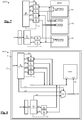
- the figure 5 shows an example architecture of the DV2 device.
- the functional entities E1, E2 and the memory MEM1 are arranged on the same interconnection support 1 or on different interconnection supports arranged in a housing 2 of the device. Only the functional entity E1 is represented, the functional entity E2 being of the same architecture and of the same arrangement, replacing the reference "I1" by the reference "12".
- the device DV2 comprises a data bus DTB, an address bus ADB, and an address multiplexer 15 controlled by a control signal CT, the output of which is connected to the address bus ADB.
- the control signal CT is provided by a bus arbitrator, not shown, which grants each of the entities periods of access to the memory MEM1 on requests thereof, and manages the access priorities.
- the memory MEM1 comprises a data input / output DIO connected to the data bus DTB and an address input AIN connected to the address bus ADB.
- the functional entity E1 comprises an address output connected to an input of the address multiplexer 15, the other input receives an address output of the functional entity E2 (not shown).
- the inverse transformation function I1 comprises a data input connected to the data bus DTB, for receiving transformed data T1 (DT) and an output connected to a data input of the functional entity E1, to supply the functional entity E1 DT data present in the transformed data T1 (DT).
- the functions T1, T2 and the function I1 also comprise an input connected to the address output of the functional entity E1, to use the AD address of a data item as input data for the data transformation DT in data T1 (DT) or T2 (DT) and their decoding according to the address AD.
- the device DV2 also comprises an address detector ADT having an address input connected to the address bus ADB and supplying the selection signal SEL to the functional entities E1 and E2.
- This address detector is for example a programmable circuit with secure access comprising address registers (not shown) configurable via the bus. DTB data, as shown, or via secure private links. These registers are used to define the start and end address of the shared area M3.
- the address detector ADT may be more complex and allow the programming of several address areas.
- the detector could also provide a selection signal SEL1 dedicated to the functional entity E1 and a selection signal SEL2 dedicated to the functional entity E2.
- the address detector is therefore similar to a simplified type of memory protection unit devoid of the usual functions of monitoring instructions and controlling the access rights of the functional entities E1, E2, the security of the memory MEM1 being here offered by the prediction of the functions of transformation and inverse transformation.
- the memory sharing method according to the invention is combined with the use of a real memory protection unit (MPU), which can then be configured to provide the SEL signal and thus replace the detector. of address ADT.
- MPU real memory protection unit
- the figure 6 shows an embodiment of the functional entity E1 of the figure 5 wherein the transform function T1 comprises an encoding function Fc1 and a signature function Fs1, the transform function T2 comprises an encoding function Fc2 and a signature function Fs2, and the inverse transformation function I1 comprises a decoding function Fdl and a signature verification function Fv1.
- the coding functions Fc1, Fc2 and decoding Fd1 are represented in block form and can be performed in the manner described above, in the form of a wired logic algorithm using a different key for each coding function.
- the coding functions Fc1, Fc2 each have an input connected to the data output of the functional entity E1, to receive the data DT, and optionally an input to the address output of the functional entity E1, to receive data. AD addresses, and an output connected to the DTB data bus.
- the decoding function Fd1 has an input connected to the data bus DTB, and optionally an input connected to the address output of the functional entity E1, to receive AD addresses, and an output connected to the data input of the functional entity E1.
- the input and the output of data of the functional entity E1 represented as distinct in the figure can be formed by the same binary port.
- the signature functions Fs1, Fs2 are realized here by means of an EXCLUSIVE OR (“XOR") logic gate G1 having an input receiving the signal SEL and N inputs receiving bits b0-bn-1 of a coded data item.
- Fc1 (DT), Fc2 (DT) provided by the function Fc1, respectively Fc2.
- the output of the gate G1 provides a parity bit of the coded data Fc1 (DT) or an inverted parity bit of the coded data Fc2 (DT).
- the parity bit or the inverted parity bit is concatenated with the bits of the coded data item as a "bn" bit of highest weight to form a coded data item signed b0-bn-1 // bn in which the bit bn forms the signature S1 or the signature S2, ie a data item Fc1 (DT) // S1 or Fc2 (DT) // S2.
- the concatenation may consist in adding a conductive track to the N tracks carrying the bits, the assembly being directly connected to the data bus DTB, which then comprises N + 1 bits, or connected to the data bus via a buffer circuit (not shown).
- the signature verification function Fv1 is carried out here by means of two doors G2, G3 of the EXCLUSIVE OR type.
- Gate G2 has an input receiving a configuration bit bc of fixed value 0 or 1, and N inputs receiving bits b0-bn-1 of coded data Fc1 (DT) or Fc2 (DT) provided by the data bus. DTB after reading the memory MEM1 (not shown, Cf. Fig. 5 ).
- the bits b0-bn-1 are also applied to the data input of the decoding function Fd1.
- the configuration bit bc is here equal to 0 and the output of the gate G2 provides a parity bit bn 'which is a function of the data bits b0-bn-1, which is applied to an input of the gate G3.
- the latter receives on another input the parity bit bn taken from the data bus DTB and supplies the error signal ER which is equal to 1 when the parity bits bn and bn 'are different, which indicates that the data read in the memory was corrupted during storage or that the data was written into the memory by the functional entity E2 and therefore has an inverted parity bit.
- the figure 7 shows another embodiment DV3 of a device according to the invention in which the functional entity E1 is a trusted entity, for example a CPU of a secure processor, designated "master" entity.
- the functional entity E2 is then a "slave” entity, it is for example a direct access memory processor "DMA"("Direct Memory Access”).
- the DMA processor forming the functional entity E2 comprises a serial input SIN connected to various peripheral processors which can thus directly access the memory MEM1 without going through the functional entity E1.
- the memory comprises a memory zone M3 which is as previously accessible for reading and writing to the two functional entities E1, E2.
- the objective here is to use the memory area M3 as the data exchange area of the functional entity E1 to the functional entity E2 and of the functional entity E2 to the functional entity E1.
- the functional entity E1 is assigned the function T2 of the functional entity E2 and its inverse transformation function I2, in addition to its own transformation function T1 and its inverse transformation function I1.
- entity Functional E2 only has its own T2 transformation and I2 inverse transformation functions.
- the functional entity E1 uses the transformation function T2 to write T2 data (DT) for the functional entity E2 in the memory area M3, and can use the transformation function T1 to write in the memory area M1 or in the memory area M3 T1 data (DT) that are not intended for the functional entity E2 and can not be read by it.
- T2 data DT
- the data T2 (DT) can also be read by the functional entity E1 because it has here the inverse transformation function I2.
- the functional entity E2 uses its transformation function T2 to write T2 data (DT) for the functional entity E1 in the memory area M3, which the functional entity E1 can read by virtue of the inverse transformation function. I2, or to write in the memory area M1 T2 data (DT) specific to it, but that the functional entity E1 could also read here being master of the memory.
- the functional entity E1 uses, as previously, a selection signal SEL on the one hand to select the transformation function T1 or the transformation function T2 when writing a data item in the memory zone M1 or M3 (it could also write data in the memory area M2 of the functional entity E2), and secondly to select the inverse transformation function I1 or the inverse transformation function I2 when reading a data item in the memory area M1 or M3.
- This selection signal is not provided here by an address detector ADT as before, but by the entity itself E1 as the memory master entity of the memory.
- the figure 8 shows an example architecture of the DV3 device.
- the functional entities E1, E2 and the memory MEM1 are arranged on the same interconnection support 1 or on different interconnection supports arranged in a housing 2 of the device.
- the device DV3 comprises, as before, the data bus DTB and the address bus ADB, and the address multiplexer 15 controlled by the control signal CT.
- the control signal CT is here supplied by the functional entity E1 which is here designated as arbitrator of the address bus and grants access periods to the memory MEM1 to the functional entity E2 and the peripheral processors, on request of the functional entity E2 or peripheral processors.
- the memory MEM1 comprises, as before, a data input / output DIO connected to the data bus DTB and an address input AIN connected to the address bus ADB.
- the functional entity E1 comprises an address output connected to an input of the address multiplexer 15 whose other input receives the address output of the functional entity E2.
- the transformation functions T1, T2 of the functional entity E1 each include a output connected to the data bus DTB and an input connected to a data output of the functional entity E1.
- the inverse transformation functions I1, I2 of the functional entity E1 each comprise a data input connected to the data bus, and an output connected to a data input of the functional entity E1.
- the transformation function T2 of the functional entity E2 comprises an output connected to the data bus DTB and an input connected to a data output of the functional entity E2.
- the inverse transformation function I2 of the functional entity E2 comprises a data input connected to the data bus, and an output connected to a data input of the functional entity E2.
- this embodiment can also be implemented in a software form, the inputs and outputs then being themselves software.
- a device according to the invention is susceptible of various other embodiments.
- a memory sharing method according to the invention may be applied to devices having a number of entities greater than 2 and more than one shared memory.
- the memory or memories can be volatile memories (RAM), programmable memories and electrically erasable (EEPROM, Flash), or other types of memory.
- RAM volatile memories
- EEPROM electrically erasable
- Flash electrically erasable
- a device according to the invention can comprise multiple private memory areas and multiple shared memory areas, and the same entity can be assigned several private memory areas.
- a device according to the invention is also capable of various applications.
- a device according to the invention may for example form all or part of a mobile phone, a radio-television decoder, a smart card, etc.
Landscapes
- Engineering & Computer Science (AREA)
- Theoretical Computer Science (AREA)
- Physics & Mathematics (AREA)
- Computer Security & Cryptography (AREA)
- General Engineering & Computer Science (AREA)
- General Physics & Mathematics (AREA)
- Computer Hardware Design (AREA)
- Software Systems (AREA)
- Human Computer Interaction (AREA)
- General Health & Medical Sciences (AREA)
- Bioethics (AREA)
- Health & Medical Sciences (AREA)
- Mathematical Physics (AREA)
- Storage Device Security (AREA)
Claims (22)
- Verfahren zum gemeinsamen Nutzen eines Speichers in einer Vorrichtung (DV1, DV2, DV3), die mindestens einen Speicher (MEM1) und mindestens zwei Funktionseinheiten (E1, E2) umfasst, die auf demselben Träger (1) oder in demselben Gehäuse (2) angeordnet sind, umfassend die Schritte, die darin bestehen,- eine erste Funktionseinheit (E1) dafür zu konfigurieren, dass sie Daten in mindestens einen ersten Bereich (M1) des Speichers schreibt und Daten aus diesem ersten Bereich ausliest,- eine zweite Funktionseinheit (E2) dafür zu konfigurieren, dass sie Daten in mindestens einen zweiten Bereich (M2) des Speichers, der vom ersten Speicherbereich (M1) getrennt ist, schreibt und Daten aus diesem zweiten Bereich ausliest,dadurch gekennzeichnet, dass es die folgenden Schritte umfasst, die darin bestehen,- der ersten Funktionseinheit (E1) eine erste Daten-Transformationsfunktion (T1) und eine erste Daten-Rücktransformationsfunktion (I1), welche die Wiederherstellung und/oder Überprüfung der Gültigkeit der mittels der ersten Transformationsfunktion transformierten Daten ermöglicht, zuzuordnen,- der zweiten Funktionseinheit (E2) eine zweite Daten-Transformationsfunktion (T2) und eine zweite Daten-Rücktransformationsfunktion welche die Wiederherstellung und/oder Überprüfung der Gültigkeit der mittels der zweiten Transformationsfunktion transformierten Daten ermöglicht, zuzuordnen, wobei die zweite Rücktransformationsfunktion (I2) mit der ersten Transformationsfunktion (T1) inkompatibel ist und die erste Rücktransformationsfunktion (I1) mit der zweiten Transformationsfunktion (T2) inkompatibel ist,- die erste Funktionseinheit (E1) dafür zu konfigurieren, dass sie die erste Transformationsfunktion (T1) auf eine Dateneinheit anwendet, bevor sie diese in den ersten Speicherbereich (M1) schreibt, und die erste Rücktransformationsfunktion (I1) auf eine aus dem ersten Speicherbereich (M1) ausgelesene Dateneinheit anwendet,- die zweite Funktionseinheit (E2) dafür zu konfigurieren, dass sie die zweite Transformationsfunktion (T2) auf eine Dateneinheit anwendet, bevor sie diese in den zweiten Speicherbereich (M2) schreibt, und die zweite Rücktransformationsfunktion (I2) auf eine aus dem zweiten Speicherbereich (M2) ausgelesene Dateneinheit anwendet.
- Verfahren nach Anspruch 1, umfassend einen Schritt, der darin besteht, mindestens die zweite Rücktransformationsfunktion (I2) dafür zu konfigurieren, dass sie bei der Rücktransformation einer mittels der ersten Transformationsfunktion (T1) transformierten Dateneinheit eine Fehlerinformation (ER) liefert.
- Verfahren nach Anspruch 2, umfassend einen Schritt, der darin besteht, eine Schutzmaßnahme gegen einen Versuch der zweiten Funktionseinheit (E2), Daten aus dem ersten Speicherbereich (M1) auszulesen, durchzuführen, wenn die zweite Rücktransformationsfunktion (I2) nach einem Auslesen einer Dateneinheit aus dem Speicher die Fehlerinformation (ER) liefert.
- Verfahren nach einem der Ansprüche 1 bis 3, umfassend die Schritte, die darin bestehen,- die erste Funktionseinheit (E1) dafür zu konfigurieren, dass sie Daten auch in einen dritten Speicherbereich (M3) schreibt,- die zweite Funktionseinheit (E2) dafür zu konfigurieren, dass sie Daten auch aus dem dritten Speicherbereich (M3) ausliest,- der ersten Funktionseinheit (E1) zusätzlich zur ersten Transformationsfunktion (T1) die zweite Transformationsfunktion (T2) zuzuordnen, ohne ihr die zweite Rücktransformationsfunktion (I2) zuzuordnen, und- die erste Funktionseinheit (E1) dafür zu konfigurieren, dass sie die zweite Transformationsfunktion (T2) auf Daten anwendet, die in den dritten Speicherbereich (M3) geschrieben werden und für die zweite Funktionseinheit (E2, DMA) bestimmt sind.
- Verfahren nach Anspruch 4, umfassend die Schritte, die darin bestehen,- die erste Funktionseinheit (E1) dafür zu konfigurieren, dass sie Daten auch aus dem dritten Speicherbereich (M3) ausliest,- die zweite Funktionseinheit (E2) dafür zu konfigurieren, dass sie Daten auch in den dritten Speicherbereich (M3) schreibt,- der zweiten Funktionseinheit (E2) zusätzlich zur zweiten Transformationsfunktion (T2) die erste Transformationsfunktion (T1) zuzuordnen, ohne ihr die erste Rücktransformationsfunktion (I1) zuzuordnen, und- die zweite Funktionseinheit (E2) dafür zu konfigurieren, dass sie die erste Transformationsfunktion (T1) auf für die erste Funktionseinheit bestimmte Daten anwendet, die in den dritten Speicherbereich (M3) geschrieben werden.
- Verfahren nach einem der Ansprüche 1 bis 3, umfassend die Schritte, die darin bestehen,- die erste und die zweite Funktionseinheit (E1, E2) dafür zu konfigurieren, dass sie Daten in einen dritten Speicherbereich (M3) schreiben und Daten aus diesem auslesen,- der ersten Funktionseinheit (E1, CPU) zusätzlich zur ersten Transformationsfunktion (T1) und zur ersten Rücktransformationsfunktion (I1) die zweite Transformationsfunktion (T2) und die zweite Rücktransformationsfunktion (I2) zuzuordnen,- der zweiten Funktionseinheit (E2, DMA) weder die erste Transformationsfunktion (T1) noch die erste Rücktransformationsfunktion (I1) zuzuordnen,- die erste Funktionseinheit (E1, CPU) dafür zu konfigurieren, dass sie die zweite Transformationsfunktion (T2) auf Daten anwendet, die in den dritten Speicherbereich geschrieben werden und für die zweite Funktionseinheit (E2, DMA) bestimmt sind.
- Verfahren nach einem der Ansprüche 1 bis 6, umfassend die Schritte, die darin bestehen,- die erste Funktionseinheit dafür zu konfigurieren, dass die erste Transformationsfunktion (T1) das Hinzufügen eines Paritätsbits (bn) zu einer zu schreibenden Dateneinheit umfasst, und dafür, dass die erste Rücktransformationsfunktion (I1) das Verifizieren, dass eine aus dem Speicher ausgelesene Dateneinheit ein gültiges Paritätsbit aufweist, umfasst und- die zweite Funktionseinheit dafür zu konfigurieren, dass die zweite Transformationsfunktion (T2) das Hinzufügen eines invertierten Paritätsbits (/bn) zu einer zu schreibenden Dateneinheit umfasst, und dafür, dass die zweite Rücktransformationsfunktion (I2) das Verifizieren, dass eine aus dem Speicher ausgelesene Dateneinheit ein gültiges invertiertes Paritätsbit aufweist, umfasst.
- Verfahren nach einem der Ansprüche 1 bis 7, umfassend den Schritt, der darin besteht, mindestens eine Funktionseinheit dafür zu konfigurieren, dass ihre Transformationsfunktion (T1, T2) eine Datencodierfunktion (Fc1, Fc2) umfasst.
- Verfahren nach Anspruch 8, umfassend den Schritt, der darin besteht, eine Codierfunktion bereitzustellen, welche die Adresse (AD) für das Schreiben der Dateneinheit in den Speicher als Codiervariable der Dateneinheit verwendet.
- Verfahren nach einem der Ansprüche 1 bis 9, umfassend den Schritt, der darin besteht, mindestens eine Funktionseinheit dafür zu konfigurieren, dass ihre Transformationsfunktion (T1, T2) eine Datensignaturfunktion (Fs1, Fs2) umfasst und ihre Rücktransformationsfunktion (11, 12) eine Signaturprüffunktion (Fv1, Fv2) umfasst, die beim Lesen einer Dateneinheit, die nicht mittels der Signaturfunktion (Fs1, Fs2) transformiert wurde, eine Fehlerinformation (ER) liefert.
- Verfahren nach einem der Ansprüche 1 bis 10, wobei mindestens eine der Funktionseinheiten aus der Gruppe ausgewählt ist, die Steuerungen des direkten Speicherzugriffs (DMA), Signalverarbeitungsprozessoren (CPU) oder Softwarefunktionen, die von einem oder mehreren Prozessoren ausgeführt werden, umfasst.
- Vorrichtung (DV1, DV2, DV3), die mindestens einen Speicher (MEM1) und mindestens zwei Funktionseinheiten (E1, E2), die auf demselben Träger (1) oder in demselben Gehäuse (2) angeordnet sind, umfasst, wobei- eine erste Funktionseinheit (E1) dafür konfiguriert ist, Daten in mindestens einen ersten Bereich (M1) des Speichers zu schreiben oder Daten aus diesem ersten Bereich auszulesen,- eine zweite Funktionseinheit (E2) dafür konfiguriert ist, Daten in mindestens einen zweiten Bereich (M2) des Speichers, der vom ersten Speicherbereich (M1) getrennt ist, zu schreiben oder Daten aus diesem zweiten Bereich auszulesen,dadurch gekennzeichnet, dass- die erste Funktionseinheit (E1) eine erste Daten-Transformationsfunktion (T1) und eine erste Daten-Rücktransformationsfunktion (I1), welche die Wiederherstellung und/oder Überprüfung der Gültigkeit von mittels der ersten Transformationsfunktion transformierten Daten ermöglicht, umfasst,- die zweite Funktionseinheit (E2) eine zweite Daten-Transformationsfunktion (T2) und eine zweite Daten-Rücktransformationsfunktion welche die Wiederherstellung und/oder Überprüfung der Gültigkeit von mittels der zweiten Transformationsfunktion transformierten Daten ermöglicht, umfasst, wobei die zweite Rücktransformationsfunktion (I2) mit der ersten Transformationsfunktion (T1) inkompatibel ist und die erste Rücktransformationsfunktion (I1) mit der zweiten Transformationsfunktion (T2) inkompatibel ist,- die erste Funktionseinheit (E1) dafür konfiguriert ist, die erste Transformationsfunktion (T1) auf eine Dateneinheit anzuwenden, bevor sie diese in den ersten Speicherbereich (M1) schreibt, und die erste Rücktransformationsfunktion (I1) auf eine aus dem ersten Speicherbereich (M1) ausgelesene Dateneinheit anzuwenden, und- die zweite Funktionseinheit (E2) dafür konfiguriert ist, die zweite Transformationsfunktion (T2) auf eine Dateneinheit anzuwenden, bevor sie diese in den zweiten Speicherbereich (M2) schreibt, und die zweite Rücktransformationsfunktion (I2) auf eine aus dem zweiten Speicherbereich (M2) ausgelesene Dateneinheit anzuwenden.
- Vorrichtung nach Anspruch 12, wobei die zweite Rücktransformationsfunktion (I2) dafür konfiguriert ist, bei der Rücktransformation einer mittels der ersten Transformationsfunktion (T1) transformierten Dateneinheit eine Fehlerinformation (ER) zu liefern.
- Vorrichtung nach Anspruch 13, wobei die zweite Funktionseinheit (E2) dafür konfiguriert ist, eine Schutzmaßnahme gegen einen Versuch der zweiten Funktionseinheit (E2), Daten aus dem ersten Speicherbereich (M1) auszulesen, durchzuführen, wenn die zweite Rücktransformationsfunktion (I2) nach einem durch die zweite Funktionseinheit (E2) erfolgten Auslesen einer Dateneinheit aus dem Speicher die Fehlerinformation (ER) liefert.
- Vorrichtung (DV2) nach einem der Ansprüche 12 bis 14, wobei- die erste Funktionseinheit (E1) dafür konfiguriert ist, Daten auch in einen dritten Speicherbereich (M3) zu schreiben,- die zweite Funktionseinheit (E2) dafür konfiguriert ist, Daten auch aus dem dritten Speicherbereich (M3) auszulesen,- die erste Funktionseinheit (E1) zusätzlich zur ersten Transformationsfunktion (T1) die zweite Transformationsfunktion (T2) umfasst, jedoch nicht die zweite Rücktransformationsfunktion (I2) umfasst, und- die erste Funktionseinheit (E1) dafür konfiguriert ist, die zweite Transformationsfunktion (T2) auf Daten anzuwenden, die in den dritten Speicherbereich (M3) geschrieben werden und für die zweite Funktionseinheit (E2, DMA) bestimmt sind.
- Vorrichtung nach Anspruch 15, wobei- die erste Funktionseinheit (E1) dafür konfiguriert ist, Daten auch aus dem dritten Speicherbereich (M3) auszulesen,- die zweite Funktionseinheit (E2) dafür konfiguriert ist, Daten auch in den dritten Speicherbereich (M3) zu schreiben,- die zweite Funktionseinheit (E2) zusätzlich zur zweiten Transformationsfunktion die erste Transformationsfunktion (T1) umfasst, jedoch nicht die erste Rücktransformationsfunktion (I1) umfasst, und- die zweite Funktionseinheit (E2) dafür konfiguriert ist, die erste Transformationsfunktion (T1) auf für die erste Funktionseinheit bestimmte Daten anzuwenden, die in den dritten Speicherbereich (M3) geschrieben werden.
- Vorrichtung (DV3) nach einem der Ansprüche 12 bis 14, wobei- die erste und die zweite Funktionseinheit (E1, E2) dafür konfiguriert sind, Daten in einen dritten Speicherbereich (M3) zu schreiben und Daten aus diesem auszulesen,- die erste Funktionseinheit (E1, CPU) zusätzlich zur ersten Transformationsfunktion (T1) und zur ersten Rücktransformationsfunktion (I1) die zweite Transformationsfunktion (T2) und die zweite Rücktransformationsfunktion (I2) umfasst,- die zweite Funktionseinheit (E2, DMA) weder die erste Transformationsfunktion (T1) noch die erste Rücktransformationsfunktion (I1) umfasst, und- die erste Funktionseinheit (E1, CPU) dafür konfiguriert ist, die zweite Transformationsfunktion (T2) auf Daten anzuwenden, die in den dritten Speicherbereich geschrieben werden und für die zweite Funktionseinheit (E2, DMA) bestimmt sind.
- Vorrichtung nach einem der Ansprüche 12 bis 17, wobei- die erste Transformationsfunktion (T1) das Hinzufügen eines Paritätsbits (bn) zu einer zu schreibenden Dateneinheit umfasst und die erste Rücktransformationsfunktion (I1) das Verifizieren, dass eine aus dem Speicher ausgelesene Dateneinheit ein gültiges Paritätsbit aufweist, umfasst, und- die zweite Transformationsfunktion (T2) das Hinzufügen eines invertierten Paritätsbits (/bn) zu einer zu schreibenden Dateneinheit umfasst, und die zweite Rücktransformationsfunktion (I2) das Verifizieren, dass eine aus dem Speicher ausgelesene Dateneinheit ein gültiges invertiertes Paritätsbit aufweist, umfasst.
- Vorrichtung nach einem der Ansprüche 12 bis 18, wobei die Transformationsfunktion (T1, T2) mindestens einer Funktionseinheit eine Datencodierfunktion (Fc1, Fc2) umfasst.
- Vorrichtung nach Anspruch 19, wobei die Codierfunktion die Adresse (AD) für das Schreiben der Dateneinheit in den Speicher als Codiervariable der Dateneinheit verwendet.
- Vorrichtung nach einem der Ansprüche 12 bis 20, wobei die Transformationsfunktion (T1, T2) mindestens einer Funktionseinheit eine Datensignaturfunktion (Fs1, Fs2) umfasst und die entsprechende Rücktransformationsfunktion (11, 12) eine Signaturprüffunktion (Fv1, Fv2) umfasst, die beim Lesen einer Dateneinheit, die nicht mittels der Signaturfunktion (Fs1, Fs2) transformiert wurde, eine Fehlerinformation (ER) liefert.
- Vorrichtung nach einem der Ansprüche 12 bis 20, wobei mindestens eine der Funktionseinheiten aus der Gruppe ausgewählt ist, die Steuerungen des direkten Speicherzugriffs (DMA), Signalverarbeitungsprozessoren (CPU) oder Softwarefunktionen, die von einem oder mehreren Prozessoren ausgeführt werden, umfasst.
Applications Claiming Priority (2)
| Application Number | Priority Date | Filing Date | Title |
|---|---|---|---|
| FR1553369A FR3035241B1 (fr) | 2015-04-16 | 2015-04-16 | Procede de partage d'une memoire entre au moins deux entites fonctionnelles |
| PCT/FR2016/050801 WO2016166450A1 (fr) | 2015-04-16 | 2016-04-07 | Procede de partage d'une memoire entre au moins deux entites fonctionnelles |
Publications (2)
| Publication Number | Publication Date |
|---|---|
| EP3283968A1 EP3283968A1 (de) | 2018-02-21 |
| EP3283968B1 true EP3283968B1 (de) | 2019-03-20 |
Family
ID=55236433
Family Applications (1)
| Application Number | Title | Priority Date | Filing Date |
|---|---|---|---|
| EP16730870.9A Active EP3283968B1 (de) | 2015-04-16 | 2016-04-07 | Verfahren zur gemeinsamen nutzung eines speichers zwischen mindestens zwei funktionelle einheiten |
Country Status (5)
| Country | Link |
|---|---|
| US (1) | US10496301B2 (de) |
| EP (1) | EP3283968B1 (de) |
| CN (1) | CN107466400B (de) |
| FR (1) | FR3035241B1 (de) |
| WO (1) | WO2016166450A1 (de) |
Families Citing this family (3)
| Publication number | Priority date | Publication date | Assignee | Title |
|---|---|---|---|---|
| CN107451494B (zh) * | 2017-06-30 | 2020-05-22 | 杭州旗捷科技有限公司 | 一种芯片改写设备的数据保护方法、电子设备及存储介质 |
| CN115237659B (zh) * | 2021-04-23 | 2026-04-10 | 伊姆西Ip控股有限责任公司 | 编码方法、电子设备和程序产品 |
| FR3129499B1 (fr) * | 2021-11-25 | 2024-06-28 | Stmicroelectronics Grand Ouest Sas | Gestion dynamique d’un pare-feu de mémoire |
Family Cites Families (21)
| Publication number | Priority date | Publication date | Assignee | Title |
|---|---|---|---|---|
| JPH0630245A (ja) * | 1992-05-23 | 1994-02-04 | Takayama:Kk | 画像処理装置 |
| JP2002342164A (ja) * | 2001-05-22 | 2002-11-29 | Hitachi Ltd | 記憶装置及びデータ処理装置並びに記憶部制御方法 |
| JP3866597B2 (ja) * | 2002-03-20 | 2007-01-10 | 株式会社東芝 | 内部メモリ型耐タンパプロセッサおよび秘密保護方法 |
| JP4338989B2 (ja) * | 2003-02-20 | 2009-10-07 | パナソニック株式会社 | メモリデバイス |
| US7827156B2 (en) * | 2003-02-26 | 2010-11-02 | Microsoft Corporation | Issuing a digital rights management (DRM) license for content based on cross-forest directory information |
| CN1802813A (zh) * | 2003-06-05 | 2006-07-12 | 松下电器产业株式会社 | 用于接收许可的用户终端 |
| EP1542181A1 (de) * | 2003-12-11 | 2005-06-15 | Banksys S.A. | Elektronische Datenverarbeitungseinrichtung |
| US20050198062A1 (en) * | 2004-03-05 | 2005-09-08 | Shapiro Richard B. | Method and apparatus for accelerating data access operations in a database system |
| KR100634566B1 (ko) * | 2005-10-06 | 2006-10-16 | 엠텍비젼 주식회사 | 공유 메모리 제어 방법 및 공유 메모리 동작 제어를수행하는 사용자 단말기 |
| US20070157030A1 (en) * | 2005-12-30 | 2007-07-05 | Feghali Wajdi K | Cryptographic system component |
| US7616206B1 (en) * | 2006-06-16 | 2009-11-10 | Nvidia Corporation | Efficient multi-chip GPU |
| US7966465B2 (en) * | 2008-01-17 | 2011-06-21 | Broadcom Corporation | Method and system for secure code encryption for PC-slave devices |
| US20100106758A1 (en) * | 2008-10-24 | 2010-04-29 | Microsoft Corporation | Computing discrete fourier transforms |
| US8352719B2 (en) * | 2009-07-31 | 2013-01-08 | Cleversafe, Inc. | Computing device booting utilizing dispersed storage |
| US20120110303A1 (en) * | 2010-10-28 | 2012-05-03 | International Business Machines Corporation | Method for Process Synchronization of Embedded Applications in Multi-Core Systems |
| US9753864B2 (en) * | 2011-06-15 | 2017-09-05 | Nokia Technologies Oy | Method and apparatus for implementing memory segment access control in a distributed memory environment |
| FR2989801B1 (fr) * | 2012-04-18 | 2014-11-21 | Schneider Electric Ind Sas | Procede de gestion securisee d'un espace memoire pour microcontroleur |
| US9430384B2 (en) * | 2013-03-31 | 2016-08-30 | Intel Corporation | Instructions and logic to provide advanced paging capabilities for secure enclave page caches |
| US9922200B2 (en) * | 2014-06-30 | 2018-03-20 | Microsoft Technology Licensing, Llc | Securely storing content within public clouds |
| US20160232088A1 (en) * | 2014-07-17 | 2016-08-11 | Sandisk Enterprise Ip Llc | Garbage Collection in Storage System with Distributed Processors |
| US10089964B2 (en) * | 2015-12-18 | 2018-10-02 | Intel Corporation | Graphics processor logic for encoding increasing or decreasing values |
-
2015
- 2015-04-16 FR FR1553369A patent/FR3035241B1/fr not_active Expired - Fee Related
-
2016
- 2016-04-07 EP EP16730870.9A patent/EP3283968B1/de active Active
- 2016-04-07 WO PCT/FR2016/050801 patent/WO2016166450A1/fr not_active Ceased
- 2016-04-07 CN CN201680021722.2A patent/CN107466400B/zh active Active
-
2017
- 2017-10-13 US US15/784,007 patent/US10496301B2/en active Active
Also Published As
| Publication number | Publication date |
|---|---|
| FR3035241B1 (fr) | 2017-12-22 |
| US20180039438A1 (en) | 2018-02-08 |
| FR3035241A1 (fr) | 2016-10-21 |
| CN107466400B (zh) | 2020-12-04 |
| CN107466400A (zh) | 2017-12-12 |
| EP3283968A1 (de) | 2018-02-21 |
| WO2016166450A1 (fr) | 2016-10-20 |
| US10496301B2 (en) | 2019-12-03 |
Similar Documents
| Publication | Publication Date | Title |
|---|---|---|
| CA2121410C (fr) | Dispositif de protection des cles d'une carte a puce | |
| US10318765B2 (en) | Protecting critical data structures in an embedded hypervisor system | |
| US10069860B1 (en) | Protection for computing systems from revoked system updates | |
| KR20230042346A (ko) | 마스터 키 에스크로 프로세스 | |
| US20070297606A1 (en) | Multiple key security and method for electronic devices | |
| FR2948795A1 (fr) | Detecteur d'injection de fautes dans un circuit integre | |
| EP3283968B1 (de) | Verfahren zur gemeinsamen nutzung eines speichers zwischen mindestens zwei funktionelle einheiten | |
| FR2976147A1 (fr) | Schema d'entrelacement de donnees pour une memoire externe d'un microcontroleur securise | |
| FR2979443A1 (fr) | Microcontroleur securise a base de mode | |
| US20220038270A1 (en) | Data processing system and method | |
| EP1983436B1 (de) | Kontrolle der Integrität eines prozessorexternen Speichers | |
| FR2806858A1 (fr) | Procede cryptographique de protection contre la fraude | |
| EP1489517B1 (de) | Schutz eines auf ausführungwartenden Programms in einem Speicher für einen Mikroprozessor | |
| Kiš et al. | A cybersecurity case for the adoption of blockchain in the financial industry | |
| FR2923923A1 (fr) | Verification de donnees lues en memoire | |
| WO2006061481A1 (fr) | Dispositif et procede de controle d’acces, noyau a composants le comportant et son utilisation | |
| KR20170095780A (ko) | 클락 윌슨 모델을 적용한 모바일 장치 및 그것의 동작 방법 | |
| FR2890202A1 (fr) | Demonstration d'une modification des donnees d'un ensemble de donnees | |
| FR2889005A1 (fr) | Integrite materielle permanente des donnees | |
| EP3026555B1 (de) | Verwaltungsverfahren einer architektur, und entsprechende architektur | |
| FR3132365A1 (fr) | Mémoire non volatile sécurisée | |
| FR3161046A1 (fr) | Procédé de protection d’un microcontrôleur | |
| CN106709329B (zh) | 由处理单元处理期间对经加密的信息的保护 | |
| Manzhosov et al. | Polymorphic Error Correction | |
| McLean et al. | Dependence on Cyberscribes-issues in e-Security |
Legal Events
| Date | Code | Title | Description |
|---|---|---|---|
| STAA | Information on the status of an ep patent application or granted ep patent |
Free format text: STATUS: THE INTERNATIONAL PUBLICATION HAS BEEN MADE |
|
| PUAI | Public reference made under article 153(3) epc to a published international application that has entered the european phase |
Free format text: ORIGINAL CODE: 0009012 |
|
| STAA | Information on the status of an ep patent application or granted ep patent |
Free format text: STATUS: REQUEST FOR EXAMINATION WAS MADE |
|
| 17P | Request for examination filed |
Effective date: 20170927 |
|
| AK | Designated contracting states |
Kind code of ref document: A1 Designated state(s): AL AT BE BG CH CY CZ DE DK EE ES FI FR GB GR HR HU IE IS IT LI LT LU LV MC MK MT NL NO PL PT RO RS SE SI SK SM TR |
|
| AX | Request for extension of the european patent |
Extension state: BA ME |
|
| DAV | Request for validation of the european patent (deleted) | ||
| DAX | Request for extension of the european patent (deleted) | ||
| GRAP | Despatch of communication of intention to grant a patent |
Free format text: ORIGINAL CODE: EPIDOSNIGR1 |
|
| STAA | Information on the status of an ep patent application or granted ep patent |
Free format text: STATUS: GRANT OF PATENT IS INTENDED |
|
| INTG | Intention to grant announced |
Effective date: 20181019 |
|
| GRAS | Grant fee paid |
Free format text: ORIGINAL CODE: EPIDOSNIGR3 |
|
| GRAA | (expected) grant |
Free format text: ORIGINAL CODE: 0009210 |
|
| STAA | Information on the status of an ep patent application or granted ep patent |
Free format text: STATUS: THE PATENT HAS BEEN GRANTED |
|
| AK | Designated contracting states |
Kind code of ref document: B1 Designated state(s): AL AT BE BG CH CY CZ DE DK EE ES FI FR GB GR HR HU IE IS IT LI LT LU LV MC MK MT NL NO PL PT RO RS SE SI SK SM TR |
|
| REG | Reference to a national code |
Ref country code: GB Ref legal event code: FG4D Free format text: NOT ENGLISH |
|
| REG | Reference to a national code |
Ref country code: CH Ref legal event code: EP |
|
| REG | Reference to a national code |
Ref country code: DE Ref legal event code: R096 Ref document number: 602016011355 Country of ref document: DE |
|
| REG | Reference to a national code |
Ref country code: AT Ref legal event code: REF Ref document number: 1111230 Country of ref document: AT Kind code of ref document: T Effective date: 20190415 |
|
| REG | Reference to a national code |
Ref country code: IE Ref legal event code: FG4D Free format text: LANGUAGE OF EP DOCUMENT: FRENCH |
|
| REG | Reference to a national code |
Ref country code: NL Ref legal event code: MP Effective date: 20190320 |
|
| PG25 | Lapsed in a contracting state [announced via postgrant information from national office to epo] |
Ref country code: SE Free format text: LAPSE BECAUSE OF FAILURE TO SUBMIT A TRANSLATION OF THE DESCRIPTION OR TO PAY THE FEE WITHIN THE PRESCRIBED TIME-LIMIT Effective date: 20190320 Ref country code: NO Free format text: LAPSE BECAUSE OF FAILURE TO SUBMIT A TRANSLATION OF THE DESCRIPTION OR TO PAY THE FEE WITHIN THE PRESCRIBED TIME-LIMIT Effective date: 20190620 Ref country code: FI Free format text: LAPSE BECAUSE OF FAILURE TO SUBMIT A TRANSLATION OF THE DESCRIPTION OR TO PAY THE FEE WITHIN THE PRESCRIBED TIME-LIMIT Effective date: 20190320 Ref country code: LT Free format text: LAPSE BECAUSE OF FAILURE TO SUBMIT A TRANSLATION OF THE DESCRIPTION OR TO PAY THE FEE WITHIN THE PRESCRIBED TIME-LIMIT Effective date: 20190320 |
|
| REG | Reference to a national code |
Ref country code: LT Ref legal event code: MG4D |
|
| PG25 | Lapsed in a contracting state [announced via postgrant information from national office to epo] |
Ref country code: BG Free format text: LAPSE BECAUSE OF FAILURE TO SUBMIT A TRANSLATION OF THE DESCRIPTION OR TO PAY THE FEE WITHIN THE PRESCRIBED TIME-LIMIT Effective date: 20190620 Ref country code: GR Free format text: LAPSE BECAUSE OF FAILURE TO SUBMIT A TRANSLATION OF THE DESCRIPTION OR TO PAY THE FEE WITHIN THE PRESCRIBED TIME-LIMIT Effective date: 20190621 Ref country code: NL Free format text: LAPSE BECAUSE OF FAILURE TO SUBMIT A TRANSLATION OF THE DESCRIPTION OR TO PAY THE FEE WITHIN THE PRESCRIBED TIME-LIMIT Effective date: 20190320 Ref country code: LV Free format text: LAPSE BECAUSE OF FAILURE TO SUBMIT A TRANSLATION OF THE DESCRIPTION OR TO PAY THE FEE WITHIN THE PRESCRIBED TIME-LIMIT Effective date: 20190320 Ref country code: HR Free format text: LAPSE BECAUSE OF FAILURE TO SUBMIT A TRANSLATION OF THE DESCRIPTION OR TO PAY THE FEE WITHIN THE PRESCRIBED TIME-LIMIT Effective date: 20190320 Ref country code: RS Free format text: LAPSE BECAUSE OF FAILURE TO SUBMIT A TRANSLATION OF THE DESCRIPTION OR TO PAY THE FEE WITHIN THE PRESCRIBED TIME-LIMIT Effective date: 20190320 |
|
| REG | Reference to a national code |
Ref country code: AT Ref legal event code: MK05 Ref document number: 1111230 Country of ref document: AT Kind code of ref document: T Effective date: 20190320 |
|
| REG | Reference to a national code |
Ref country code: DE Ref legal event code: R081 Ref document number: 602016011355 Country of ref document: DE Owner name: VERIMATRIX, FR Free format text: FORMER OWNER: INSIDE SECURE, MEYREUIL, FR Ref country code: DE Ref legal event code: R081 Ref document number: 602016011355 Country of ref document: DE Owner name: RAMBUS INC., SUNNYVALE, US Free format text: FORMER OWNER: INSIDE SECURE, MEYREUIL, FR |
|
| PG25 | Lapsed in a contracting state [announced via postgrant information from national office to epo] |
Ref country code: RO Free format text: LAPSE BECAUSE OF FAILURE TO SUBMIT A TRANSLATION OF THE DESCRIPTION OR TO PAY THE FEE WITHIN THE PRESCRIBED TIME-LIMIT Effective date: 20190320 Ref country code: SK Free format text: LAPSE BECAUSE OF FAILURE TO SUBMIT A TRANSLATION OF THE DESCRIPTION OR TO PAY THE FEE WITHIN THE PRESCRIBED TIME-LIMIT Effective date: 20190320 Ref country code: CZ Free format text: LAPSE BECAUSE OF FAILURE TO SUBMIT A TRANSLATION OF THE DESCRIPTION OR TO PAY THE FEE WITHIN THE PRESCRIBED TIME-LIMIT Effective date: 20190320 Ref country code: EE Free format text: LAPSE BECAUSE OF FAILURE TO SUBMIT A TRANSLATION OF THE DESCRIPTION OR TO PAY THE FEE WITHIN THE PRESCRIBED TIME-LIMIT Effective date: 20190320 Ref country code: IT Free format text: LAPSE BECAUSE OF FAILURE TO SUBMIT A TRANSLATION OF THE DESCRIPTION OR TO PAY THE FEE WITHIN THE PRESCRIBED TIME-LIMIT Effective date: 20190320 Ref country code: ES Free format text: LAPSE BECAUSE OF FAILURE TO SUBMIT A TRANSLATION OF THE DESCRIPTION OR TO PAY THE FEE WITHIN THE PRESCRIBED TIME-LIMIT Effective date: 20190320 Ref country code: PT Free format text: LAPSE BECAUSE OF FAILURE TO SUBMIT A TRANSLATION OF THE DESCRIPTION OR TO PAY THE FEE WITHIN THE PRESCRIBED TIME-LIMIT Effective date: 20190720 Ref country code: AL Free format text: LAPSE BECAUSE OF FAILURE TO SUBMIT A TRANSLATION OF THE DESCRIPTION OR TO PAY THE FEE WITHIN THE PRESCRIBED TIME-LIMIT Effective date: 20190320 |
|
| PG25 | Lapsed in a contracting state [announced via postgrant information from national office to epo] |
Ref country code: PL Free format text: LAPSE BECAUSE OF FAILURE TO SUBMIT A TRANSLATION OF THE DESCRIPTION OR TO PAY THE FEE WITHIN THE PRESCRIBED TIME-LIMIT Effective date: 20190320 Ref country code: SM Free format text: LAPSE BECAUSE OF FAILURE TO SUBMIT A TRANSLATION OF THE DESCRIPTION OR TO PAY THE FEE WITHIN THE PRESCRIBED TIME-LIMIT Effective date: 20190320 |
|
| REG | Reference to a national code |
Ref country code: CH Ref legal event code: PL |
|
| REG | Reference to a national code |
Ref country code: BE Ref legal event code: MM Effective date: 20190430 |
|
| PG25 | Lapsed in a contracting state [announced via postgrant information from national office to epo] |
Ref country code: AT Free format text: LAPSE BECAUSE OF FAILURE TO SUBMIT A TRANSLATION OF THE DESCRIPTION OR TO PAY THE FEE WITHIN THE PRESCRIBED TIME-LIMIT Effective date: 20190320 Ref country code: LU Free format text: LAPSE BECAUSE OF NON-PAYMENT OF DUE FEES Effective date: 20190407 Ref country code: IS Free format text: LAPSE BECAUSE OF FAILURE TO SUBMIT A TRANSLATION OF THE DESCRIPTION OR TO PAY THE FEE WITHIN THE PRESCRIBED TIME-LIMIT Effective date: 20190720 |
|
| REG | Reference to a national code |
Ref country code: DE Ref legal event code: R097 Ref document number: 602016011355 Country of ref document: DE |
|
| PLBE | No opposition filed within time limit |
Free format text: ORIGINAL CODE: 0009261 |
|
| STAA | Information on the status of an ep patent application or granted ep patent |
Free format text: STATUS: NO OPPOSITION FILED WITHIN TIME LIMIT |
|
| REG | Reference to a national code |
Ref country code: DE Ref legal event code: R081 Ref document number: 602016011355 Country of ref document: DE Owner name: RAMBUS INC., SUNNYVALE, US Free format text: FORMER OWNER: VERIMATRIX, MEYREUIL, FR |
|
| PG25 | Lapsed in a contracting state [announced via postgrant information from national office to epo] |
Ref country code: LI Free format text: LAPSE BECAUSE OF NON-PAYMENT OF DUE FEES Effective date: 20190430 Ref country code: CH Free format text: LAPSE BECAUSE OF NON-PAYMENT OF DUE FEES Effective date: 20190430 Ref country code: DK Free format text: LAPSE BECAUSE OF FAILURE TO SUBMIT A TRANSLATION OF THE DESCRIPTION OR TO PAY THE FEE WITHIN THE PRESCRIBED TIME-LIMIT Effective date: 20190320 Ref country code: MC Free format text: LAPSE BECAUSE OF FAILURE TO SUBMIT A TRANSLATION OF THE DESCRIPTION OR TO PAY THE FEE WITHIN THE PRESCRIBED TIME-LIMIT Effective date: 20190320 |
|
| 26N | No opposition filed |
Effective date: 20200102 |
|
| PG25 | Lapsed in a contracting state [announced via postgrant information from national office to epo] |
Ref country code: SI Free format text: LAPSE BECAUSE OF FAILURE TO SUBMIT A TRANSLATION OF THE DESCRIPTION OR TO PAY THE FEE WITHIN THE PRESCRIBED TIME-LIMIT Effective date: 20190320 Ref country code: BE Free format text: LAPSE BECAUSE OF NON-PAYMENT OF DUE FEES Effective date: 20190430 |
|
| REG | Reference to a national code |
Ref country code: GB Ref legal event code: 732E Free format text: REGISTERED BETWEEN 20200227 AND 20200304 |
|
| PG25 | Lapsed in a contracting state [announced via postgrant information from national office to epo] |
Ref country code: TR Free format text: LAPSE BECAUSE OF FAILURE TO SUBMIT A TRANSLATION OF THE DESCRIPTION OR TO PAY THE FEE WITHIN THE PRESCRIBED TIME-LIMIT Effective date: 20190320 |
|
| PG25 | Lapsed in a contracting state [announced via postgrant information from national office to epo] |
Ref country code: IE Free format text: LAPSE BECAUSE OF NON-PAYMENT OF DUE FEES Effective date: 20190407 |
|
| PG25 | Lapsed in a contracting state [announced via postgrant information from national office to epo] |
Ref country code: CY Free format text: LAPSE BECAUSE OF FAILURE TO SUBMIT A TRANSLATION OF THE DESCRIPTION OR TO PAY THE FEE WITHIN THE PRESCRIBED TIME-LIMIT Effective date: 20190320 |
|
| PG25 | Lapsed in a contracting state [announced via postgrant information from national office to epo] |
Ref country code: HU Free format text: LAPSE BECAUSE OF FAILURE TO SUBMIT A TRANSLATION OF THE DESCRIPTION OR TO PAY THE FEE WITHIN THE PRESCRIBED TIME-LIMIT; INVALID AB INITIO Effective date: 20160407 Ref country code: MT Free format text: LAPSE BECAUSE OF FAILURE TO SUBMIT A TRANSLATION OF THE DESCRIPTION OR TO PAY THE FEE WITHIN THE PRESCRIBED TIME-LIMIT Effective date: 20190320 |
|
| PG25 | Lapsed in a contracting state [announced via postgrant information from national office to epo] |
Ref country code: MK Free format text: LAPSE BECAUSE OF FAILURE TO SUBMIT A TRANSLATION OF THE DESCRIPTION OR TO PAY THE FEE WITHIN THE PRESCRIBED TIME-LIMIT Effective date: 20190320 |
|
| PGFP | Annual fee paid to national office [announced via postgrant information from national office to epo] |
Ref country code: DE Payment date: 20250429 Year of fee payment: 10 |
|
| PGFP | Annual fee paid to national office [announced via postgrant information from national office to epo] |
Ref country code: FR Payment date: 20250425 Year of fee payment: 10 |
|
| PGFP | Annual fee paid to national office [announced via postgrant information from national office to epo] |
Ref country code: GB Payment date: 20260327 Year of fee payment: 11 |