EP3285308B1 - Oled-substrat, herstellungsverfahren dafür und anzeigevorrichtung - Google Patents
Oled-substrat, herstellungsverfahren dafür und anzeigevorrichtung Download PDFInfo
- Publication number
- EP3285308B1 EP3285308B1 EP15883650.2A EP15883650A EP3285308B1 EP 3285308 B1 EP3285308 B1 EP 3285308B1 EP 15883650 A EP15883650 A EP 15883650A EP 3285308 B1 EP3285308 B1 EP 3285308B1
- Authority
- EP
- European Patent Office
- Prior art keywords
- pattern
- metal extending
- extending portion
- cathode
- layer
- Prior art date
- Legal status (The legal status is an assumption and is not a legal conclusion. Google has not performed a legal analysis and makes no representation as to the accuracy of the status listed.)
- Active
Links
Images
Classifications
-
- H—ELECTRICITY
- H10—SEMICONDUCTOR DEVICES; ELECTRIC SOLID-STATE DEVICES NOT OTHERWISE PROVIDED FOR
- H10K—ORGANIC ELECTRIC SOLID-STATE DEVICES
- H10K59/00—Integrated devices, or assemblies of multiple devices, comprising at least one organic light-emitting element covered by group H10K50/00
- H10K59/10—OLED displays
- H10K59/12—Active-matrix OLED [AMOLED] displays
- H10K59/122—Pixel-defining structures or layers, e.g. banks
-
- H—ELECTRICITY
- H10—SEMICONDUCTOR DEVICES; ELECTRIC SOLID-STATE DEVICES NOT OTHERWISE PROVIDED FOR
- H10D—INORGANIC ELECTRIC SEMICONDUCTOR DEVICES
- H10D86/00—Integrated devices formed in or on insulating or conducting substrates, e.g. formed in silicon-on-insulator [SOI] substrates or on stainless steel or glass substrates
-
- H—ELECTRICITY
- H10—SEMICONDUCTOR DEVICES; ELECTRIC SOLID-STATE DEVICES NOT OTHERWISE PROVIDED FOR
- H10K—ORGANIC ELECTRIC SOLID-STATE DEVICES
- H10K50/00—Organic light-emitting devices
- H10K50/80—Constructional details
- H10K50/805—Electrodes
- H10K50/81—Anodes
- H10K50/813—Anodes characterised by their shape
-
- H—ELECTRICITY
- H10—SEMICONDUCTOR DEVICES; ELECTRIC SOLID-STATE DEVICES NOT OTHERWISE PROVIDED FOR
- H10K—ORGANIC ELECTRIC SOLID-STATE DEVICES
- H10K50/00—Organic light-emitting devices
- H10K50/80—Constructional details
- H10K50/805—Electrodes
- H10K50/81—Anodes
- H10K50/814—Anodes combined with auxiliary electrodes, e.g. ITO layer combined with metal lines
-
- H—ELECTRICITY
- H10—SEMICONDUCTOR DEVICES; ELECTRIC SOLID-STATE DEVICES NOT OTHERWISE PROVIDED FOR
- H10K—ORGANIC ELECTRIC SOLID-STATE DEVICES
- H10K50/00—Organic light-emitting devices
- H10K50/80—Constructional details
- H10K50/805—Electrodes
- H10K50/82—Cathodes
- H10K50/824—Cathodes combined with auxiliary electrodes
-
- H—ELECTRICITY
- H10—SEMICONDUCTOR DEVICES; ELECTRIC SOLID-STATE DEVICES NOT OTHERWISE PROVIDED FOR
- H10K—ORGANIC ELECTRIC SOLID-STATE DEVICES
- H10K59/00—Integrated devices, or assemblies of multiple devices, comprising at least one organic light-emitting element covered by group H10K50/00
- H10K59/10—OLED displays
- H10K59/12—Active-matrix OLED [AMOLED] displays
- H10K59/131—Interconnections, e.g. wiring lines or terminals
-
- H—ELECTRICITY
- H10—SEMICONDUCTOR DEVICES; ELECTRIC SOLID-STATE DEVICES NOT OTHERWISE PROVIDED FOR
- H10K—ORGANIC ELECTRIC SOLID-STATE DEVICES
- H10K71/00—Manufacture or treatment specially adapted for the organic devices covered by this subclass
- H10K71/10—Deposition of organic active material
- H10K71/12—Deposition of organic active material using liquid deposition, e.g. spin coating
- H10K71/13—Deposition of organic active material using liquid deposition, e.g. spin coating using printing techniques, e.g. ink-jet printing or screen printing
-
- H—ELECTRICITY
- H10—SEMICONDUCTOR DEVICES; ELECTRIC SOLID-STATE DEVICES NOT OTHERWISE PROVIDED FOR
- H10K—ORGANIC ELECTRIC SOLID-STATE DEVICES
- H10K50/00—Organic light-emitting devices
- H10K50/10—OLEDs or polymer light-emitting diodes [PLED]
- H10K50/11—OLEDs or polymer light-emitting diodes [PLED] characterised by the electroluminescent [EL] layers
-
- H—ELECTRICITY
- H10—SEMICONDUCTOR DEVICES; ELECTRIC SOLID-STATE DEVICES NOT OTHERWISE PROVIDED FOR
- H10K—ORGANIC ELECTRIC SOLID-STATE DEVICES
- H10K50/00—Organic light-emitting devices
- H10K50/80—Constructional details
- H10K50/805—Electrodes
- H10K50/82—Cathodes
- H10K50/822—Cathodes characterised by their shape
-
- H—ELECTRICITY
- H10—SEMICONDUCTOR DEVICES; ELECTRIC SOLID-STATE DEVICES NOT OTHERWISE PROVIDED FOR
- H10K—ORGANIC ELECTRIC SOLID-STATE DEVICES
- H10K59/00—Integrated devices, or assemblies of multiple devices, comprising at least one organic light-emitting element covered by group H10K50/00
- H10K59/10—OLED displays
- H10K59/12—Active-matrix OLED [AMOLED] displays
- H10K59/1201—Manufacture or treatment
Definitions
- the present invention belongs to the field of display technology, particularly to an OLED substrate and a manufacturing method thereof, a display device.
- the organic light-emitting device has broad application prospects because it has the advantages of simple manufacturing process, low cost, low power consumption, high luminance, wide adaptation range of the working temperature etc.
- the OLED has extremely wide applications in the aspect of display.
- an OLED substrate is taken as an example for illustration.
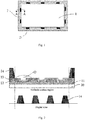
- the OLED substrate comprises a display area 1, and a peripheral area 2 around the display area 1, and the peripheral area 2 comprises a plurality of cathode contact regions 21.
- a source-drain (SD) metal extending portion 11 is formed on a base substrate 10 of the OLED substrate. The source-drain metal extending portion 11 extends from the display area to the cathode contact regions of the peripheral area.
- SD source-drain
- a passivation layer 12 (PVX) is formed on a layer where the source-drain metal extending portion 11 locates, and a plurality of via holes are formed in the passivation layer 12 located in the cathode contact regions.
- An anode and an anode metal extending portion of the OLED device are formed on the passivation layer 12.
- the anode of the OLED device is located in the display area, and is arranged in a same layer as the anode metal extending portion 13.
- the anode metal extending portion 13 also extends from the display area to the cathode contact regions of the peripheral area.
- the anode metal extending portion 13 is connected with the source-drain metal extending portion 11 at the cathode contact regions through the via holes.
- a pixel definition layer 14 is formed on the layer where the anode and the anode metal extending portion of the OLED device locate.
- the pixel definition layer 14 comprises first openings located in the display area and second openings located in the cathode contact regions of the peripheral area. Each of the first openings is used for accommodating the light emitting material of an OLED device.
- the width of the second opening is much larger than the width of the first opening, and the width of the second opening is even larger than the width of the cathode contact region.
- the cathode and the cathode metal extending portion of the OLED device are formed.
- the cathode of the OLED device is located in the display area and is connected with the anode metal extending portion 13.
- the cathode metal extending portion extends from the display area to the cathode contact regions of the peripheral area.
- US2003184217 , US2005179377 or US2011095299 all show cathode contact regions in the periphery of an OLED display the cathode contact regions featuring the pixel definition layer having a groove.
- the pixel definition layer in the cathode contact region of US2015090966 features several grooves.
- the first opening in the display area 1 approximately can accommodate 2-6 Q regions as shown in Fig. 2 , while Fig. 1 is only a schematic representation. Therefore, how to avoid the organic light emitting material from being formed at positions where the via hole locate is an urgent problem to be solved.
- the technical problem to be solved by the present invention includes, with respect to the above problem in the existing OLED substrate, providing an OLED substrate, for which the cleaning is convenient and even the step of cleaning up the light emitting material may be omitted, a manufacturing method thereof, and a display device.
- an OLED substrate may be divided into a display area and a peripheral area around the display area, the peripheral area having a plurality of cathode contact regions.
- the OLED substrate comprises: a base substrate, a source-drain metal extending portion arranged on the base substrate, and the source-drain metal extending portion extending from the display area to the cathode contact regions of the peripheral area, a passivation layer arranged on a layer where the source-drain metal extending portion locates, and the passivation layer having a plurality of via holes at positions corresponding to the cathode contact regions, an anode metal extending portion arranged on the passivation layer, and the anode metal extending portion extending from the display area to the cathode contact regions of the peripheral area and being electrically connected with the source-drain metal extending portion through the via holes, a pixel definition layer arranged on a layer where the anode metal extending portion locates, and the pixel
- a width of the protrusion portion of the first pattern is same as a width of the groove portion of the second pattern, and a width of the groove portion of the first pattern is same as a width of the protrusion portion of the second pattern.
- the OLED substrate further comprises a light emitting material layer, the light emitting material layer is arranged in the groove portion of the first pattern and on the protrusion portion of the second pattern.
- the OLED substrate further comprises a cathode and a cathode metal extending portion connected with the cathode.
- the cathode and the cathode metal extending portion are arranged on the light emitting material layer, and the cathode is arranged in the display area, the cathode metal extending portion extends from the display area to the cathode contact regions of the peripheral area and is connected with the anode metal extending portion through the groove portion of the second pattern.
- the OLED substrate further comprises an anode arranged in the display area, and the anode is arranged in a same layer as the anode metal extending portion and is disconnected from the anode metal extending portion.
- a manufacturing method of an OLED substrate comprising the steps of:
- a width of the protrusion portion of the first pattern is same as a width of the groove portion of the second pattern, and a width of the groove portion of the first pattern is same as a width of the protrusion portion of the second pattern.
- the method further comprises forming a light emitting material layer, the light emitting material layer is formed in the groove portion of the first pattern and on the protrusion portion of the second pattern.
- the light emitting material layer is formed by continuous printing.
- the method further comprises forming a pattern comprising a cathode and a cathode metal extending portion connected with the cathode through a patterning process.
- the cathode and the cathode metal extending portion are arranged on the light emitting material layer, and the cathode is arranged in the display area, the cathode metal extending portion extends from the display area to the cathode contact regions of the peripheral area and is connected with the anode metal extending portion through the groove portion of the second pattern.
- an anode is further formed while forming the anode metal extending portion, and the anode is arranged in a same layer as the anode metal extending portion and is disconnected from the anode metal extending portion.
- a display device comprising an OLED substrate as described above is provided.
- the present invention has the following beneficial effect:
- the pixel definition layer of the present invention has a plurality of successively arranged first patterns at positions corresponding to the display area and a plurality of successively arranged second patterns at positions corresponding to the cathode contact regions of the peripheral area, moreover, the protrusion portion of the first pattern corresponds to the groove portion of the second pattern, and the groove portion of the first pattern corresponds to the protrusion portion of the second pattern; in other words, the first pattern and the second pattern are opposite patterns.
- the light emitting material when printing a light emitting material in the pixel definition layer by continuous printing so as to form a light emitting material layer of the OLED device, the light emitting material will not be printed into the groove portion of the second pattern while only being left on the protrusion portion of the second pattern, thus the problem of being difficult to clean up the light emitting material falling into positions under the groove portion of the second pattern corresponding to the via holes of the passivation layer is avoided.
- this embodiment provides an OLED substrate. Because the planar schematic view of the OLED substrate of this embodiment is same as the prior art, both are represented by Fig. 1 .
- the OLED substrate is divided into a display area 1 and a peripheral area 2 around the display area 1.
- the peripheral area 2 has a plurality of cathode contact regions 21.
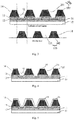
- the OLED substrate of this embodiment comprises: a base substrate 10; a source-drain metal extending portion 11, arranged on the base substrate 10, and the source-drain metal extending portion 11 extending from the display area 1 to the cathode contact regions 21 of the peripheral area 2; a passivation layer 12, arranged on a layer where the source-drain metal extending portion 11 locates, and the passivation layer 12 having a plurality of via holes at positions corresponding to the cathode contact regions 21; an anode metal extending portion 13, arranged on the passivation layer 12, and the anode metal extending portion 13 extending from the display area 1 to the cathode contact regions 21 of the peripheral area 2 and being electrically connected with the source-drain metal extending portion 11 through the via holes; a pixel definition layer 14, arranged on a layer where the anode metal extending portion 13 locates, and the pixel definition layer 14 having a plurality of successively arranged first patterns 100 at positions corresponding to the display area 1, each of the first patterns 100 having
- the pixel definition layer 14 has a plurality of successively arranged first patterns 100 at positions corresponding to the display area 1 and has a plurality of successively arranged second patterns 200 at positions corresponding to the cathode contact regions 21 of the peripheral area 2, moreover, the protrusion portion 102 of the first pattern corresponds to the groove portion 201 of the second pattern, and the groove portion 101 of the first pattern corresponds to the protrusion portion 202 of the second pattern.
- the first pattern 100 and the second pattern 200 are opposite patterns.
- the continuous printing means printing successively in a row direction or a column direction where the groove portion 101 of the first pattern locates.
- the groove portions and the protrusion portions of the first pattern 100 and the second pattern 200 have exactly opposite positions, when it is printed to the second pattern 200, the light emitting material can only be printed to the position of the protrusion portion of the second pattern 200.
- the groove portion 101 of the first pattern located in the display area 1 for example can correspond to a size of about 2-6 Q positions.
- Fig. 3 is only a schematic representation.
- Respective layer structures of a thin film transistor e.g. a gate layer, a gate insulating layer, an active layer, a source and a drain etc., can also be arranged on the base substrate 10.
- the source-drain metal extending portion 11 is arranged in a same layer as the source and the drain.
- a width of the protrusion portion 102 of the first pattern is same as a width of the groove portion 201 of the second pattern, and a width of the groove portion 101 of the first pattern is same as a width of the protrusion portion 202 of the second pattern.
- the OLED substrate of this embodiment further comprises a light emitting material layer 15.
- the light emitting material layer 15 is arranged in the groove portion 101 of the first pattern and on the protrusion portion 202 of the second pattern. That is to say, when printing the light emitting material continuously so as to form the light emitting material layer 15, in the display area 1, the light emitting material falls into the groove portion 101 of each first pattern, so as to form a light emitting material layer 15 of each OLED light emitting unit.
- the light emitting material falls onto the protrusion portion 202 of the second pattern, thereby enabling the light emitting material to be kept on the protrusion portion 202 of the second pattern while not having to be cleaned up, which improves the production efficiency.
- the light emitting material on the protrusion portion 202 of the second pattern can also be cleaned up.
- the material of the pixel definition layer 14 can be a hydrophobic material, hence, when the light emitting material is printed onto the protrusion portion 202 of the second pattern, it will not flow into the groove portion 201 of the second pattern either.
- the OLED substrate of this embodiment further comprises a cathode, and a cathode metal extending portion 16 connected with the cathode.
- the cathode and the cathode metal extending portion 16 are arranged on the light emitting material layer 15, and the cathode is arranged in the display area 1.
- the cathode metal extending portion 16 extends from the display area 1 to the cathode contact regions 21 of the peripheral area 2, and is connected with the anode metal extending portion 13 through the groove portion 201 of the second pattern.
- a signal required by the cathode can be inputted at the positions of the cathode contact regions 21.
- the OLED substrate of this embodiment further comprises an anode arranged in the display area 1.
- the anode is arranged in a same layer as the anode metal extending portion 13 and is disconnected from the anode metal extending portion 13. It can be understood that each OLED light emitting unit formed on the OLED substrate has a separate anode. Each anode is driven by a thin film transistor in a corresponding pixel unit.
- the structure of the OLED substrate provided by this embodiment solves the problem of being difficult to clean up the light emitting material of the existing OLED substrate.
- This embodiment provides a manufacturing method of an OLED substrate, which can be used for manufacturing the OLED substrate in Embodiment 1.
- the manufacturing method comprises: Step I, forming, on a base substrate 10, a pattern comprising a source-drain metal extending portion 11 through a patterning process, the source-drain metal extending portion 11 extending from a display area 1 to cathode contact regions 21 of a peripheral area 2.
- the method may further comprise forming respective layer structures of the thin film transistor on the base substrate 10.
- the source-drain metal extending portion 11 can be formed with the source and the drain of the thin film transistor by one patterning process, so as to simplify the process.
- the base substrate 10 in this step for example can be made from a transparent material such as glass, resin, sapphire or quartz, and is pre-cleaned.
- a source-drain metal film can be formed on the base substrate 10 by sputtering, thermal evaporation or chemical vapor deposition (CVD). Photoresist coating, exposing, developing, etching, and photoresist stripping are performed to the source-drain metal film so as to form a pattern comprising the source-drain metal extending portion 11.
- the material of the source-drain metal film can be one of Mo, MoNb, Al, AINd, Ti and Cu.
- the source-drain metal film can be a monolayer or multilayer composite lamination formed by several materials of the above materials.
- it can be a monolayer or multilayer composite film consisting of Mo, Al or an alloy containing Mo, Al.
- Step II forming a passivation layer 12 on the base substrate 10 where the above step has been performed, and forming a plurality of via holes at positions corresponding to the cathode contact regions 21 in the passivation layer 12 through a patterning process.
- the passivation layer 12 can be formed by means of manufacturing processes such as thermal growth, normal pressure CVD, low pressure CVD, plasma assisted CVD or sputtering. Then, a plurality of via holes penetrating through the passivation layer 12 are formed by performing photoresist coating, exposing, developing, etching, and photoresist stripping on the passivation layer 12.
- the material of the passivation layer 12 can be SiOx, SiNx, HfOx, SiON, AlOx, etc., alternatively, the passivation layer can consist of multilayer films of two or three of the above materials.
- Step III forming, on the base substrate 10 where the above steps have been performed, a pattern comprising an anode metal extending portion 13 through a patterning process, the anode metal extending portion 13 extending from the display area 1 to the cathode contact regions 21 of the peripheral area 2 and being electrically connected with the source-drain metal extending portion 11 through the via holes.
- an anode is also formed in the display area 1 at the same time.
- the anode is disconnected from the anode metal extending portion 13.
- an electrically conductive film can be deposited by sputtering, thermal evaporation or chemical vapor deposition, and the anode and the anode metal extending portion 13 can be formed through a patterning process.
- the anode is electrically connected with the drain of the thin film transistor.
- the anode metal extending portion 13 is electrically connected with the source-drain metal extending portion 11 through the via hole.
- the electrically conductive film can be a structure of ITO/Ag/ITO or a structure of Ag/ITO; alternatively, the ITO in the above structure is replaced with IZO, IGZO or InGaSnO.
- the conductive film can also be formed from an inorganic metal oxide, an organic electrically conductive polymer or a metal material with electrical conductivity and high work function value.
- the inorganic metal oxide comprises ITO or ZnO.
- the organic electrically conductive polymer comprises PEDOT:SS, PANI.
- the metal material comprises gold, copper, silver or platinum.
- Step IV forming a pixel definition layer 14 on the base substrate 10 where the above steps have been performed, and forming a plurality of successively arranged first patterns 100 at positions corresponding to the display area 1 in the pixel definition layer 14 through a patterning process, each of the first patterns 100 having a protrusion portion 102 and a groove portion 101, forming a plurality of successively arranged second patterns 200 at positions corresponding to the cathode contact regions 21 of the peripheral area 2 in the pixel definition layer 14, each of the second pattern 200 having a protrusion portion 202 and a groove portion 201, the protrusion portion 102 of the first pattern corresponding to the groove portion 201 of the second pattern, and the groove portion 101 of the first pattern corresponding to the protrusion portion 202 of the second pattern.
- the pixel definition layer 14 can be formed by means of coating. Then, through exposure, development etc., a plurality of first patterns 100 are formed at positions corresponding to the display area 1 in the pixel definition layer 14, and a plurality of second patterns 200 are formed at positions corresponding to the cathode contact regions 21 in the pixel definition layer 14.
- the material of the pixel definition layer 14 can be a lyophobic organic fluorine containing material.
- the width of the protrusion portion 102 of the first pattern for example can be same as the width of the groove portion 201 of the second pattern, and the width of the groove portion 101 of the first pattern for example can be same as the width of the protrusion portion 202 of the second pattern. The reason why it is set in such a way is for the sake of avoiding as much as possible the problem of being difficult to clean up the light emitting material falling into the groove portion 201 of the second pattern when forming the organic light emitting material layer.
- Step V forming a light emitting material layer 15 on the base substrate 10 where the above steps have been performed, the light emitting material layer being formed in the groove portion 101 of the first pattern and on the protrusion portion 202 of the second pattern.
- the light emitting material layer can be formed by continuous printing.
- Step VI forming, on the base substrate 10 where the above steps have been performed, a pattern comprising a cathode and a cathode metal extending portion 16 connected with the cathode through a patterning process.
- the cathode is formed in the display area 1, the cathode metal extending portion 16 extends from the display area 1 to the cathode contact regions 21 of the peripheral area 2 and is connected with the anode metal extending portion 13 through the groove portion 201 of the second pattern.
- the cathode and the cathode metal extending portion 16 connected with the cathode can be formed by sputtering or evaporation.
- the materials of the cathode and the cathode metal extending portion 16 are low work function metal materials, such as lithium, magnesium,, calcium, strontium, aluminum, indium or alloys of the above metals with copper, gold, silver; alternatively, the cathode and the cathode metal extending portion 16 can be composed of a very thin buffer insulating layer (e.g., LiF, CsCO 3 etc.) and the above metals or alloys.
- a very thin buffer insulating layer e.g., LiF, CsCO 3 etc.
- the OLED substrate is formed.
- This embodiment provides a display device comprising the above OLED substrate.
- the display device can be any product or component with the display function such as a mobile phone, a panel computer, a television, a display, a laptop, a digital photo frame, a navigator etc.
- the display device of this embodiment comprises the OLED substrate in Embodiment 1, its performance is better.
- the display device of this embodiment can also comprise other conventional structures, such as a power supply unit, a display driving unit etc.
Landscapes
- Engineering & Computer Science (AREA)
- Microelectronics & Electronic Packaging (AREA)
- Physics & Mathematics (AREA)
- Optics & Photonics (AREA)
- Manufacturing & Machinery (AREA)
- Electroluminescent Light Sources (AREA)
Claims (12)
- OLED-Substrat, unterteilt in einen Displaybereich (1) und einen Peripheriebereich (2) um den Displaybereich (1) herum, wobei der Peripheriebereich (2) mehrere Kathoden-Kontaktregionen (21) aufweist,
wobei das OLED-Substrat Folgendes umfasst:ein Basissubstrat (10);einen sich erstreckenden Source-Drain-Metallabschnitt (11), der auf dem Basissubstrat (10) angeordnet ist, und wobei sich der erstreckende Source-Drain-Metallabschnitt (11) von dem Displaybereich (1) zu den Kathoden-Kontaktregionen (21) des Peripheriebereichs (2) erstreckt;eine Passivierungsschicht (12), die auf einer Schicht angeordnet ist, auf der sich der sich erstreckende Source-Drain-Metallabschnitt (11) befindet, und wobei die Passivierungsschicht (12) mehrere Durchgangslöcher in Positionen aufweist, die den Kathoden-Kontaktregionen (21) entsprechen;einen sich erstreckenden Anoden-Metallabschnitt (13), der auf der Passivierungsschicht (12) angeordnet ist, und wobei der sich erstreckende Anoden-Metallabschnitt (13) sich von dem Displaybereich (1) zu den Kathoden-Kontaktregionen (21) des Peripheriebereichs (2) erstreckt und elektrisch mit dem sich erstreckenden Source-Drain-Metallabschnitt (11) durch die Durchgangslöcher verbunden ist;eine Pixel-Definitionsschicht (14), die auf einer Schicht angeordnet ist, auf der sich der sich erstreckende Anoden-Metallabschnitt (13) befindet, und wobei die Pixel-Definitionsschicht (14) mehrere nacheinander angeordnete erste Strukturen (100) an Positionen aufweist, die dem Displaybereich (1) entsprechen, wobei jede der ersten Strukturen (100) einen überstehenden Abschnitt (102) und einen Rillenabschnitt (101) aufweist; wobei die Pixel-Definitionsschicht (14) mehrere nacheinander angeordnete zweite Strukturen (200) in Positionen aufweist, die den Kathoden-Kontaktregionen (21) entsprechen, wobei jede der zweiten Strukturen (200) einen überstehenden Abschnitt (202) und einen Rillenabschnitt (201) aufweist, wobei der überstehende Abschnitt (102) der ersten Struktur (100) dem Rillenabschnitt (201) der zweiten Struktur (200) entspricht, und der Rillenabschnitt (101) der ersten Struktur (100) der überstehenden Struktur (202) der zweiten Struktur (200) entspricht. - OLED-Substrat nach Anspruch 1, wobei eine Breite des überstehenden Abschnitts (102) der ersten Struktur (100) dieselbe ist wie eine Breite des Rillenabschnitts (201) der zweiten Struktur (200), und eine Breite des Rillenabschnitts (101) der ersten Struktur (100) dieselbe ist wie eine Breite des überstehenden Abschnitts (202) der zweiten Struktur (200).
- OLED-Substrat nach Anspruch 1, ferner umfassend eine Licht emittierende Materialschicht (15), wobei die Licht emittierende Materialschicht (15) in dem Rillenabschnitt (101) der ersten Struktur (100) und auf dem überstehenden Abschnitt (202) der zweiten Struktur (200) angeordnet ist.
- OLED-Substrat nach Anspruch 3, ferner umfassend eine Kathode und einen sich erstreckenden Kathoden-Metallabschnitt (16), der mit der Kathode verbunden ist, wobei die Kathode und der sich erstreckende Kathoden-Metallabschnitt (16) auf der Licht emittierenden Materialschicht (15) angeordnet sind, und die Kathode in dem Displaybereich (1) angeordnet ist, wobei der sich erstreckende Kathoden-Metallabschnitt (16) sich von dem Displaybereich (1) zu den Kathoden-Kontaktregionen (21) des Peripheriebereichs (2) erstreckt und mit dem sich erstreckenden Anoden-Metallabschnitt (13) durch den Rillenabschnitt (201) der zweiten Struktur (200) verbunden ist.
- OLED-Substrat nach einem der Ansprüche 1 bis 4, ferner umfassend eine Anode, die in dem Displaybereich (1) angeordnet ist, wobei die Anode in einer selben Schicht wie der sich erstreckende Anoden-Metallabschnitt (13) angeordnet und von dem sich erstreckenden Anoden-Metallabschnitt (13) getrennt ist.
- Herstellungsverfahren eines OLED-Substrats, umfassend:Bilden, auf einem Basissubstrat (10), einer Struktur, die einen sich erstreckenden Source-Drain-Metallabschnitt (11) aufweist, durch einen Strukturierungsprozess, wobei der sich erstreckende Source-Drain-Metallabschnitt (11) sich von einem Displaybereich (1) zu Kathoden-Kontaktregionen (21) eines Peripheriebereichs (2) erstreckt;Bilden einer Passivierungsschicht (12) auf dem Basissubstrat (10), auf dem der obige Schritt durchgeführt wurde, und Bilden mehrerer Durchgangslöcher an Positionen, die den Kathoden-Kontaktregionen (21) entsprechen, in der Passivierungsschicht (12), durch einen Strukturierungsprozess;Bilden, auf dem Basissubstrat (10), auf dem die obigen Schritte durchgeführt wurden, einer Struktur, umfassend einen sich erstreckenden Anoden-Metallabschnitt (13) durch einen Strukturierungsprozess, wobei der sich erstreckende Anoden-Metallabschnitt (13) sich von dem Displaybereich (1) zu den Kathoden-Kontaktregionen (21) des Peripheriebereichs (2) erstreckt und elektrisch mit dem sich erstreckenden Source-Drain-Metallabschnitt (11) durch die Durchgangslöcher verbunden ist;Bilden einer Pixel-Definitionsschicht (14) auf dem Basissubstrat (10), auf dem die obigen Schritte durchgeführt wurden, und Bilden mehrerer nacheinander angeordneter erster Strukturen (100) in Positionen, die dem Displaybereich (1) entsprechen, in der Pixel-Definitionsschicht (14), durch einen Strukturierungsprozess, wobei jede der ersten Strukturen (100) einen überstehenden Abschnitt (102) und einen Rillenabschnitt (101) aufweist, Bilden mehrerer nacheinander angeordneter zweiter Strukturen (200) in Positionen, die den Kathoden-Kontaktregionen (21) des Peripheriebereichs (2) entsprechen, in der Pixel-Definitionsschicht (14), wobei jede der zweiten Strukturen (200) einen überstehenden Abschnitt (202) und einen Rillenabschnitt (201) aufweist, wobei der überstehende Abschnitt (102) der ersten Struktur (100) dem Rillenabschnitt (201) der zweiten Struktur (200) entspricht, und der Rillenabschnitt (101) der ersten Struktur (100) dem überstehenden Abschnitt (202) der zweiten Struktur (200) entspricht.
- Herstellungsverfahren eines OLED-Substrats nach Anspruch 6, wobei eine Breite des überstehenden Abschnitts (102) der ersten Struktur (100) dieselbe ist wie eine Breite des Rillenabschnitts (201) der zweiten Struktur (200), und eine Breite des Rillenabschnitts (101) der ersten Struktur (100) dieselbe ist wie eine Breite des überstehenden Abschnitts (202) der zweiten Struktur (200).
- Herstellungsverfahren eines OLED-Substrats nach Anspruch 6, wobei nach dem Schritt des Bildens der Pixel-Definitionsschicht (14) das Verfahren ferner umfasst:
Bilden einer Licht emittierenden Materialschicht (15), wobei die Licht emittierende Materialschicht (15) in dem Rillenabschnitt (101) der ersten Struktur (100) und auf dem überstehenden Abschnitt (202) der zweiten Struktur (200) gebildet ist. - Herstellungsverfahren eines OLED-Substrats nach Anspruch 8, wobei die Licht emittierende Materialschicht (15) durch Endlosdruck gebildet ist.
- Herstellungsverfahren eines OLED-Substrats nach Anspruch 9, wobei nach dem Schritt des Bildens der Licht emittierenden Materialschicht (15) das Verfahren ferner umfasst:
Bilden einer Struktur, die eine Kathode und einen sich erstreckenden Kathoden-Metallabschnitt (16) umfasst, der mit der Kathode verbunden ist, durch einen Strukturierungsprozess, wobei die Kathode und der sich erstreckende Kathoden-Metallabschnitt (16) auf der Licht emittierenden Materialschicht (15) angeordnet sind, und die Kathode in dem Displaybereich (1) angeordnet ist, wobei der sich erstreckende Kathoden-Metallabschnitt (16) sich von dem Displaybereich (1) zu den Kathoden-Kontaktregionen (21) des Peripheriebereichs (2) erstreckt und mit dem sich erstreckenden Anoden-Metallabschnitt (13) durch den Rillenabschnitt (201) der zweiten Struktur (200) verbunden ist. - Herstellungsverfahren eines OLED-Substrats nach Anspruch 6, wobei eine Anode ferner gebildet wird, während der sich erstreckende Anoden-Metallabschnitt (13) gebildet wird, wobei die Anode in einer selben Schicht wie der sich erstreckende Anoden-Metallabschnitt (13) angeordnet ist und von dem sich erstreckenden Anoden-Metallabschnitt (13) getrennt ist.
- Displayvorrichtung, umfassend ein OLED-Substrat nach einem der Ansprüche 1 bis 5.
Applications Claiming Priority (2)
| Application Number | Priority Date | Filing Date | Title |
|---|---|---|---|
| CN201510185625.4A CN104766930B (zh) | 2015-04-17 | 2015-04-17 | Oled基板及其制备方法、显示装置 |
| PCT/CN2015/085574 WO2016165238A1 (zh) | 2015-04-17 | 2015-07-30 | Oled基板及其制备方法、显示装置 |
Publications (3)
| Publication Number | Publication Date |
|---|---|
| EP3285308A1 EP3285308A1 (de) | 2018-02-21 |
| EP3285308A4 EP3285308A4 (de) | 2019-01-02 |
| EP3285308B1 true EP3285308B1 (de) | 2020-05-06 |
Family
ID=53648650
Family Applications (1)
| Application Number | Title | Priority Date | Filing Date |
|---|---|---|---|
| EP15883650.2A Active EP3285308B1 (de) | 2015-04-17 | 2015-07-30 | Oled-substrat, herstellungsverfahren dafür und anzeigevorrichtung |
Country Status (4)
| Country | Link |
|---|---|
| US (1) | US10403694B2 (de) |
| EP (1) | EP3285308B1 (de) |
| CN (1) | CN104766930B (de) |
| WO (1) | WO2016165238A1 (de) |
Families Citing this family (7)
| Publication number | Priority date | Publication date | Assignee | Title |
|---|---|---|---|---|
| CN104766930B (zh) | 2015-04-17 | 2017-07-25 | 京东方科技集团股份有限公司 | Oled基板及其制备方法、显示装置 |
| KR102582466B1 (ko) | 2016-09-21 | 2023-09-25 | 삼성디스플레이 주식회사 | 표시 장치 |
| CN107170788A (zh) * | 2017-06-06 | 2017-09-15 | 武汉华星光电技术有限公司 | 一种显示屏 |
| CN109728031B (zh) * | 2017-10-31 | 2020-03-24 | 昆山国显光电有限公司 | 有机电致发光器件、显示器及移动通信设备 |
| KR102431788B1 (ko) * | 2017-12-13 | 2022-08-10 | 엘지디스플레이 주식회사 | 표시장치 |
| CN110335889A (zh) * | 2019-07-01 | 2019-10-15 | 深圳市华星光电半导体显示技术有限公司 | 显示面板及其制备方法 |
| KR20230089244A (ko) | 2021-12-13 | 2023-06-20 | 엘지디스플레이 주식회사 | 표시 장치 |
Family Cites Families (17)
| Publication number | Priority date | Publication date | Assignee | Title |
|---|---|---|---|---|
| US7190335B2 (en) * | 2002-03-26 | 2007-03-13 | Semiconductor Energy Laboratory Co., Ltd. | Light emitting device and method of manufacturing the same |
| WO2005067352A1 (en) * | 2004-01-08 | 2005-07-21 | Samsung Electronics Co., Ltd. | Display device, and method of manufacturing the display device |
| JP3951055B2 (ja) * | 2004-02-18 | 2007-08-01 | セイコーエプソン株式会社 | 有機エレクトロルミネッセンス装置及び電子機器 |
| KR100647339B1 (ko) * | 2006-01-11 | 2006-11-23 | 삼성전자주식회사 | 평판표시장치 |
| KR20160095209A (ko) * | 2008-09-12 | 2016-08-10 | 닛토덴코 가부시키가이샤 | 섬유증 질환의 조영제 |
| KR101319096B1 (ko) * | 2009-02-24 | 2013-10-17 | 엘지디스플레이 주식회사 | 탑 에미션 인버티드형 유기발광 다이오드 표시장치 및 그의제조방법 |
| JP5593676B2 (ja) * | 2009-10-22 | 2014-09-24 | ソニー株式会社 | 表示装置および表示装置の製造方法 |
| CN101867023A (zh) | 2010-02-26 | 2010-10-20 | 信利半导体有限公司 | 一种有机电致发光显示器的封装方法 |
| KR20120103970A (ko) * | 2011-03-11 | 2012-09-20 | 삼성디스플레이 주식회사 | 유기전계발광 표시장치 |
| KR101881083B1 (ko) * | 2011-11-09 | 2018-07-24 | 삼성디스플레이 주식회사 | 유기 발광 표시 장치 |
| TWI549283B (zh) * | 2011-12-29 | 2016-09-11 | 三星顯示器有限公司 | 有機發光二極體顯示器以及製造其之方法 |
| KR20140031003A (ko) * | 2012-09-04 | 2014-03-12 | 삼성디스플레이 주식회사 | 유기 발광 표시 장치 및 그 제조 방법 |
| KR20140128080A (ko) | 2013-04-26 | 2014-11-05 | 삼성디스플레이 주식회사 | 유기 발광 표시 장치 및 그 제조 방법 |
| JP2015049972A (ja) * | 2013-08-30 | 2015-03-16 | 株式会社ジャパンディスプレイ | 有機el表示装置 |
| KR102114316B1 (ko) * | 2013-10-02 | 2020-05-25 | 삼성디스플레이 주식회사 | 유기발광 디스플레이 장치 및 그 제조방법 |
| CN103545345B (zh) * | 2013-11-11 | 2016-09-21 | 京东方科技集团股份有限公司 | 一种显示面板及其制备方法、显示装置 |
| CN104766930B (zh) * | 2015-04-17 | 2017-07-25 | 京东方科技集团股份有限公司 | Oled基板及其制备方法、显示装置 |
-
2015
- 2015-04-17 CN CN201510185625.4A patent/CN104766930B/zh active Active
- 2015-07-30 EP EP15883650.2A patent/EP3285308B1/de active Active
- 2015-07-30 US US15/124,444 patent/US10403694B2/en active Active
- 2015-07-30 WO PCT/CN2015/085574 patent/WO2016165238A1/zh not_active Ceased
Non-Patent Citations (1)
| Title |
|---|
| None * |
Also Published As
| Publication number | Publication date |
|---|---|
| WO2016165238A1 (zh) | 2016-10-20 |
| US20170084674A1 (en) | 2017-03-23 |
| EP3285308A1 (de) | 2018-02-21 |
| US10403694B2 (en) | 2019-09-03 |
| CN104766930A (zh) | 2015-07-08 |
| EP3285308A4 (de) | 2019-01-02 |
| CN104766930B (zh) | 2017-07-25 |
Similar Documents
| Publication | Publication Date | Title |
|---|---|---|
| EP3285308B1 (de) | Oled-substrat, herstellungsverfahren dafür und anzeigevorrichtung | |
| US20160005799A1 (en) | Thin film transistor, tft array substrate, manufacturing method thereof and display device | |
| US20150214249A1 (en) | Array Substrate, Display Device and Manufacturing Method | |
| CN104681629B (zh) | 薄膜晶体管、阵列基板及其各自的制备方法、显示装置 | |
| US9590177B2 (en) | Organic light-emitting display panel and fabrication method thereof | |
| CN107680993A (zh) | Oled面板及其制作方法 | |
| US11296235B2 (en) | Thin film transistor having a wire grid on a channel region and manufacturing method thereof, array substrate and manufacturing method thereof, and display panel | |
| US20210202464A1 (en) | Electrostatic Discharge Unit, Array Substrate and Display Panel | |
| US9929183B2 (en) | Array substrate, manufacturing method of array substrate and display device | |
| JP6818554B2 (ja) | アレイ基板の製造方法、アレイ基板および表示装置 | |
| US20200075773A1 (en) | Thin film transistor, method of manufacturing thin film transistor, array substrate and display panel | |
| CN105355646A (zh) | 阵列基板及其制备方法、显示装置 | |
| US9171941B2 (en) | Fabricating method of thin film transistor, fabricating method of array substrate and display device | |
| US9978876B2 (en) | Thin film transistor comprising light shielding layers, array substrate and manufacturing processes of them | |
| KR102185577B1 (ko) | Oled 기판 및 그 제조 방법 | |
| EP3159734B1 (de) | Arraysubstrat und herstellungsverfahren dafür sowie anzeigevorrichtung | |
| US20160035753A1 (en) | Complementary Thin Film Transistor and Manufacturing Method Thereof, Array Substrate, Display Apparatus | |
| CN103383945A (zh) | 一种阵列基板、显示装置及阵列基板的制造方法 | |
| CN108400151B (zh) | 显示基板及其制作方法、显示装置 | |
| US9684217B2 (en) | Array substrate, method for manufacturing the same and liquid crystal display device | |
| KR20130098709A (ko) | 박막트랜지스터 기판 및 이의 제조 방법 | |
| KR101689886B1 (ko) | 산화물 반도체를 이용한 박막트랜지스터 기판의 제조방법 | |
| US10784287B2 (en) | TFT substrate and manufacturing method thereof | |
| US9165954B2 (en) | Array substrate and method for manufacturing the same, and display device | |
| KR102039424B1 (ko) | 산화물 박막 트랜지스터의 제조방법 |
Legal Events
| Date | Code | Title | Description |
|---|---|---|---|
| STAA | Information on the status of an ep patent application or granted ep patent |
Free format text: STATUS: THE INTERNATIONAL PUBLICATION HAS BEEN MADE |
|
| PUAI | Public reference made under article 153(3) epc to a published international application that has entered the european phase |
Free format text: ORIGINAL CODE: 0009012 |
|
| STAA | Information on the status of an ep patent application or granted ep patent |
Free format text: STATUS: REQUEST FOR EXAMINATION WAS MADE |
|
| 17P | Request for examination filed |
Effective date: 20160907 |
|
| AK | Designated contracting states |
Kind code of ref document: A1 Designated state(s): AL AT BE BG CH CY CZ DE DK EE ES FI FR GB GR HR HU IE IS IT LI LT LU LV MC MK MT NL NO PL PT RO RS SE SI SK SM TR |
|
| AX | Request for extension of the european patent |
Extension state: BA ME |
|
| DAV | Request for validation of the european patent (deleted) | ||
| DAX | Request for extension of the european patent (deleted) | ||
| A4 | Supplementary search report drawn up and despatched |
Effective date: 20181130 |
|
| RIC1 | Information provided on ipc code assigned before grant |
Ipc: H01L 27/12 20060101ALI20181126BHEP Ipc: H01L 51/52 20060101AFI20181126BHEP |
|
| GRAP | Despatch of communication of intention to grant a patent |
Free format text: ORIGINAL CODE: EPIDOSNIGR1 |
|
| STAA | Information on the status of an ep patent application or granted ep patent |
Free format text: STATUS: GRANT OF PATENT IS INTENDED |
|
| INTG | Intention to grant announced |
Effective date: 20191204 |
|
| GRAS | Grant fee paid |
Free format text: ORIGINAL CODE: EPIDOSNIGR3 |
|
| GRAA | (expected) grant |
Free format text: ORIGINAL CODE: 0009210 |
|
| STAA | Information on the status of an ep patent application or granted ep patent |
Free format text: STATUS: THE PATENT HAS BEEN GRANTED |
|
| AK | Designated contracting states |
Kind code of ref document: B1 Designated state(s): AL AT BE BG CH CY CZ DE DK EE ES FI FR GB GR HR HU IE IS IT LI LT LU LV MC MK MT NL NO PL PT RO RS SE SI SK SM TR |
|
| REG | Reference to a national code |
Ref country code: GB Ref legal event code: FG4D |
|
| REG | Reference to a national code |
Ref country code: CH Ref legal event code: EP Ref country code: AT Ref legal event code: REF Ref document number: 1268262 Country of ref document: AT Kind code of ref document: T Effective date: 20200515 |
|
| REG | Reference to a national code |
Ref country code: IE Ref legal event code: FG4D |
|
| REG | Reference to a national code |
Ref country code: DE Ref legal event code: R096 Ref document number: 602015052570 Country of ref document: DE |
|
| REG | Reference to a national code |
Ref country code: LT Ref legal event code: MG4D |
|
| REG | Reference to a national code |
Ref country code: NL Ref legal event code: MP Effective date: 20200506 |
|
| PG25 | Lapsed in a contracting state [announced via postgrant information from national office to epo] |
Ref country code: LT Free format text: LAPSE BECAUSE OF FAILURE TO SUBMIT A TRANSLATION OF THE DESCRIPTION OR TO PAY THE FEE WITHIN THE PRESCRIBED TIME-LIMIT Effective date: 20200506 Ref country code: PT Free format text: LAPSE BECAUSE OF FAILURE TO SUBMIT A TRANSLATION OF THE DESCRIPTION OR TO PAY THE FEE WITHIN THE PRESCRIBED TIME-LIMIT Effective date: 20200907 Ref country code: NO Free format text: LAPSE BECAUSE OF FAILURE TO SUBMIT A TRANSLATION OF THE DESCRIPTION OR TO PAY THE FEE WITHIN THE PRESCRIBED TIME-LIMIT Effective date: 20200806 Ref country code: FI Free format text: LAPSE BECAUSE OF FAILURE TO SUBMIT A TRANSLATION OF THE DESCRIPTION OR TO PAY THE FEE WITHIN THE PRESCRIBED TIME-LIMIT Effective date: 20200506 Ref country code: GR Free format text: LAPSE BECAUSE OF FAILURE TO SUBMIT A TRANSLATION OF THE DESCRIPTION OR TO PAY THE FEE WITHIN THE PRESCRIBED TIME-LIMIT Effective date: 20200807 Ref country code: SE Free format text: LAPSE BECAUSE OF FAILURE TO SUBMIT A TRANSLATION OF THE DESCRIPTION OR TO PAY THE FEE WITHIN THE PRESCRIBED TIME-LIMIT Effective date: 20200506 Ref country code: IS Free format text: LAPSE BECAUSE OF FAILURE TO SUBMIT A TRANSLATION OF THE DESCRIPTION OR TO PAY THE FEE WITHIN THE PRESCRIBED TIME-LIMIT Effective date: 20200906 |
|
| PG25 | Lapsed in a contracting state [announced via postgrant information from national office to epo] |
Ref country code: LV Free format text: LAPSE BECAUSE OF FAILURE TO SUBMIT A TRANSLATION OF THE DESCRIPTION OR TO PAY THE FEE WITHIN THE PRESCRIBED TIME-LIMIT Effective date: 20200506 Ref country code: HR Free format text: LAPSE BECAUSE OF FAILURE TO SUBMIT A TRANSLATION OF THE DESCRIPTION OR TO PAY THE FEE WITHIN THE PRESCRIBED TIME-LIMIT Effective date: 20200506 Ref country code: RS Free format text: LAPSE BECAUSE OF FAILURE TO SUBMIT A TRANSLATION OF THE DESCRIPTION OR TO PAY THE FEE WITHIN THE PRESCRIBED TIME-LIMIT Effective date: 20200506 Ref country code: BG Free format text: LAPSE BECAUSE OF FAILURE TO SUBMIT A TRANSLATION OF THE DESCRIPTION OR TO PAY THE FEE WITHIN THE PRESCRIBED TIME-LIMIT Effective date: 20200806 |
|
| REG | Reference to a national code |
Ref country code: AT Ref legal event code: MK05 Ref document number: 1268262 Country of ref document: AT Kind code of ref document: T Effective date: 20200506 |
|
| PG25 | Lapsed in a contracting state [announced via postgrant information from national office to epo] |
Ref country code: AL Free format text: LAPSE BECAUSE OF FAILURE TO SUBMIT A TRANSLATION OF THE DESCRIPTION OR TO PAY THE FEE WITHIN THE PRESCRIBED TIME-LIMIT Effective date: 20200506 Ref country code: NL Free format text: LAPSE BECAUSE OF FAILURE TO SUBMIT A TRANSLATION OF THE DESCRIPTION OR TO PAY THE FEE WITHIN THE PRESCRIBED TIME-LIMIT Effective date: 20200506 |
|
| PG25 | Lapsed in a contracting state [announced via postgrant information from national office to epo] |
Ref country code: IT Free format text: LAPSE BECAUSE OF FAILURE TO SUBMIT A TRANSLATION OF THE DESCRIPTION OR TO PAY THE FEE WITHIN THE PRESCRIBED TIME-LIMIT Effective date: 20200506 Ref country code: ES Free format text: LAPSE BECAUSE OF FAILURE TO SUBMIT A TRANSLATION OF THE DESCRIPTION OR TO PAY THE FEE WITHIN THE PRESCRIBED TIME-LIMIT Effective date: 20200506 Ref country code: RO Free format text: LAPSE BECAUSE OF FAILURE TO SUBMIT A TRANSLATION OF THE DESCRIPTION OR TO PAY THE FEE WITHIN THE PRESCRIBED TIME-LIMIT Effective date: 20200506 Ref country code: CZ Free format text: LAPSE BECAUSE OF FAILURE TO SUBMIT A TRANSLATION OF THE DESCRIPTION OR TO PAY THE FEE WITHIN THE PRESCRIBED TIME-LIMIT Effective date: 20200506 Ref country code: DK Free format text: LAPSE BECAUSE OF FAILURE TO SUBMIT A TRANSLATION OF THE DESCRIPTION OR TO PAY THE FEE WITHIN THE PRESCRIBED TIME-LIMIT Effective date: 20200506 Ref country code: EE Free format text: LAPSE BECAUSE OF FAILURE TO SUBMIT A TRANSLATION OF THE DESCRIPTION OR TO PAY THE FEE WITHIN THE PRESCRIBED TIME-LIMIT Effective date: 20200506 Ref country code: SM Free format text: LAPSE BECAUSE OF FAILURE TO SUBMIT A TRANSLATION OF THE DESCRIPTION OR TO PAY THE FEE WITHIN THE PRESCRIBED TIME-LIMIT Effective date: 20200506 Ref country code: AT Free format text: LAPSE BECAUSE OF FAILURE TO SUBMIT A TRANSLATION OF THE DESCRIPTION OR TO PAY THE FEE WITHIN THE PRESCRIBED TIME-LIMIT Effective date: 20200506 |
|
| REG | Reference to a national code |
Ref country code: DE Ref legal event code: R097 Ref document number: 602015052570 Country of ref document: DE |
|
| PG25 | Lapsed in a contracting state [announced via postgrant information from national office to epo] |
Ref country code: SK Free format text: LAPSE BECAUSE OF FAILURE TO SUBMIT A TRANSLATION OF THE DESCRIPTION OR TO PAY THE FEE WITHIN THE PRESCRIBED TIME-LIMIT Effective date: 20200506 Ref country code: MC Free format text: LAPSE BECAUSE OF FAILURE TO SUBMIT A TRANSLATION OF THE DESCRIPTION OR TO PAY THE FEE WITHIN THE PRESCRIBED TIME-LIMIT Effective date: 20200506 Ref country code: PL Free format text: LAPSE BECAUSE OF FAILURE TO SUBMIT A TRANSLATION OF THE DESCRIPTION OR TO PAY THE FEE WITHIN THE PRESCRIBED TIME-LIMIT Effective date: 20200506 |
|
| REG | Reference to a national code |
Ref country code: CH Ref legal event code: PL |
|
| PLBE | No opposition filed within time limit |
Free format text: ORIGINAL CODE: 0009261 |
|
| STAA | Information on the status of an ep patent application or granted ep patent |
Free format text: STATUS: NO OPPOSITION FILED WITHIN TIME LIMIT |
|
| 26N | No opposition filed |
Effective date: 20210209 |
|
| REG | Reference to a national code |
Ref country code: BE Ref legal event code: MM Effective date: 20200731 |
|
| PG25 | Lapsed in a contracting state [announced via postgrant information from national office to epo] |
Ref country code: FR Free format text: LAPSE BECAUSE OF NON-PAYMENT OF DUE FEES Effective date: 20200731 Ref country code: LU Free format text: LAPSE BECAUSE OF NON-PAYMENT OF DUE FEES Effective date: 20200730 Ref country code: LI Free format text: LAPSE BECAUSE OF NON-PAYMENT OF DUE FEES Effective date: 20200731 Ref country code: CH Free format text: LAPSE BECAUSE OF NON-PAYMENT OF DUE FEES Effective date: 20200731 |
|
| PG25 | Lapsed in a contracting state [announced via postgrant information from national office to epo] |
Ref country code: BE Free format text: LAPSE BECAUSE OF NON-PAYMENT OF DUE FEES Effective date: 20200731 Ref country code: SI Free format text: LAPSE BECAUSE OF FAILURE TO SUBMIT A TRANSLATION OF THE DESCRIPTION OR TO PAY THE FEE WITHIN THE PRESCRIBED TIME-LIMIT Effective date: 20200506 |
|
| PG25 | Lapsed in a contracting state [announced via postgrant information from national office to epo] |
Ref country code: IE Free format text: LAPSE BECAUSE OF NON-PAYMENT OF DUE FEES Effective date: 20200730 |
|
| PG25 | Lapsed in a contracting state [announced via postgrant information from national office to epo] |
Ref country code: TR Free format text: LAPSE BECAUSE OF FAILURE TO SUBMIT A TRANSLATION OF THE DESCRIPTION OR TO PAY THE FEE WITHIN THE PRESCRIBED TIME-LIMIT Effective date: 20200506 Ref country code: MT Free format text: LAPSE BECAUSE OF FAILURE TO SUBMIT A TRANSLATION OF THE DESCRIPTION OR TO PAY THE FEE WITHIN THE PRESCRIBED TIME-LIMIT Effective date: 20200506 Ref country code: CY Free format text: LAPSE BECAUSE OF FAILURE TO SUBMIT A TRANSLATION OF THE DESCRIPTION OR TO PAY THE FEE WITHIN THE PRESCRIBED TIME-LIMIT Effective date: 20200506 |
|
| PG25 | Lapsed in a contracting state [announced via postgrant information from national office to epo] |
Ref country code: MK Free format text: LAPSE BECAUSE OF FAILURE TO SUBMIT A TRANSLATION OF THE DESCRIPTION OR TO PAY THE FEE WITHIN THE PRESCRIBED TIME-LIMIT Effective date: 20200506 |
|
| REG | Reference to a national code |
Ref country code: DE Ref legal event code: R079 Ref document number: 602015052570 Country of ref document: DE Free format text: PREVIOUS MAIN CLASS: H01L0051520000 Ipc: H10K0050800000 |
|
| PGFP | Annual fee paid to national office [announced via postgrant information from national office to epo] |
Ref country code: DE Payment date: 20250728 Year of fee payment: 11 |
|
| PGFP | Annual fee paid to national office [announced via postgrant information from national office to epo] |
Ref country code: GB Payment date: 20250722 Year of fee payment: 11 |