EP3285356B1 - Ladevorrichtung, elektronische vorrichtung und ladeverfahren - Google Patents
Ladevorrichtung, elektronische vorrichtung und ladeverfahren Download PDFInfo
- Publication number
- EP3285356B1 EP3285356B1 EP17186821.9A EP17186821A EP3285356B1 EP 3285356 B1 EP3285356 B1 EP 3285356B1 EP 17186821 A EP17186821 A EP 17186821A EP 3285356 B1 EP3285356 B1 EP 3285356B1
- Authority
- EP
- European Patent Office
- Prior art keywords
- pin
- charger
- electronic device
- charge
- power
- Prior art date
- Legal status (The legal status is an assumption and is not a legal conclusion. Google has not performed a legal analysis and makes no representation as to the accuracy of the status listed.)
- Not-in-force
Links
Images


Classifications
-
- H—ELECTRICITY
- H02—GENERATION; CONVERSION OR DISTRIBUTION OF ELECTRIC POWER
- H02J—ELECTRIC POWER NETWORKS; CIRCUIT ARRANGEMENTS OR SYSTEMS FOR SUPPLYING OR DISTRIBUTING ELECTRIC POWER; SYSTEMS FOR STORING ELECTRIC ENERGY
- H02J7/00—Circuit arrangements for charging or discharging batteries or for supplying loads from batteries
- H02J7/90—Regulation of charging or discharging current or voltage
- H02J7/927—Regulation of charging or discharging current or voltage with introduction of pulses during the charging process
-
- H—ELECTRICITY
- H02—GENERATION; CONVERSION OR DISTRIBUTION OF ELECTRIC POWER
- H02J—ELECTRIC POWER NETWORKS; CIRCUIT ARRANGEMENTS OR SYSTEMS FOR SUPPLYING OR DISTRIBUTING ELECTRIC POWER; SYSTEMS FOR STORING ELECTRIC ENERGY
- H02J7/00—Circuit arrangements for charging or discharging batteries or for supplying loads from batteries
- H02J7/40—Circuit arrangements for charging or discharging batteries or for supplying loads from batteries characterised by the exchange of charge or discharge related data
- H02J7/42—Circuit arrangements for charging or discharging batteries or for supplying loads from batteries characterised by the exchange of charge or discharge related data with electronic devices having internal batteries, e.g. mobile phones
-
- H—ELECTRICITY
- H02—GENERATION; CONVERSION OR DISTRIBUTION OF ELECTRIC POWER
- H02J—ELECTRIC POWER NETWORKS; CIRCUIT ARRANGEMENTS OR SYSTEMS FOR SUPPLYING OR DISTRIBUTING ELECTRIC POWER; SYSTEMS FOR STORING ELECTRIC ENERGY
- H02J7/00—Circuit arrangements for charging or discharging batteries or for supplying loads from batteries
- H02J7/40—Circuit arrangements for charging or discharging batteries or for supplying loads from batteries characterised by the exchange of charge or discharge related data
- H02J7/47—Arrangements for checking compatibility or authentication between one component, e.g. a battery or a battery charger, and another component, e.g. a power source
Definitions
- This disclosure relates to an electronic device, and more particularly relates to an electronic device with a rechargeable battery, a charger to charge the electronic device, and a charging method thereof.
- Document D1 discloses a power adaptor (100) comprising a power conversion unit (110) and a power supply line (121), and the power conversion unit (110) charges a terminal (200) by means of the power supply line (121).
- the power adaptor (100) further comprises a communication unit (130) and a data line (122).
- the communication unit (130) communicates with the terminal (200) by means of the data line (122) when the power adaptor (100) is connected to the terminal (200), and the power adaptor (100) charges the terminal (200) using the power supply line (121), and the power adaptor (100) communicates with the terminal (200) by means of the data line (122).
- Document D2 discloses a quick method comprising: upon determining that an electronic device has successfully performed a handshake with a USB host device via a USB interface, measuring, according to a preset charging current threshold, a corresponding charging data set of the electronic device at the charging current threshold (S101), the charging current threshold comprising at least a first charging current threshold and a second charging current threshold, and the charging data set comprising at least a corresponding first charging voltage value and first charging current value of the electronic device at the first charging current threshold and a corresponding second charging voltage value and second charging current value of the electronic device at the second charging current threshold.
- S101 preset charging current threshold
- the charging current threshold comprising at least a first charging current threshold and a second charging current threshold
- the charging data set comprising at least a corresponding first charging voltage value and first charging current value of the electronic device at the first charging current threshold and a corresponding second charging voltage value and second charging current value of the electronic device at the second charging current threshold.
- Document D3 discloses a method for continuously detecting when a USB client device may be charged according to a BCS charging standard. Power is supplied from a USB host device to the USB client device with a first current limit. Next, the USB host device monitors data lines D+ and D- for a first part of a handshake. When the first part of the handshake is detected, a second part of the handshake is provided by the USB host device indicating that the USB client device may be changed according to the BCS charging standard. All current sources and all voltage sources that are coupled to the data lines D+ and D- are decoupled from data lines D+ and D- after the handshake is complete.
- Embodiments of the disclosure provide a charger, an electronic device, and a charging method, to enhance charge speed by using normal charge ports and a normal charge cable.
- the disclosure provides a charger that comprises: a charge port, a controller, and a connection switching circuit.
- the charge port comprises a power pin, a first data pin, a second data pin, and a ground pin, the first data pin is disconnected to the second data pin, the charge port is configured to connect to an electronic device.
- the controller is connected to the first data pin and the second data pin.
- the connection switching circuit is connected to the power pin, the first data pin, the second data pin, and the ground pin, and the controller. Therein, the controller is configured to control the connection switching circuit to connect the first data pin to the power pin and connect the second data pin to the ground pin, when a handshake between the charger and the electronic device connected to the charge port is created successfully.
- the disclosure further provides an electronic device that comprises a power port, a processor, and a connection switching circuit.
- the power port comprises a power pin, a first data pin, a second data pin, and a ground pin, the first data pin is disconnected to the second data pin, the power port is configured to connect to a charger.
- the processor is connected to the first data pin and the second data pin.
- the connection switching circuit is connected to the power pin, the first data pin, the second data pin, and the ground pin, and the processor.
- the processor is configured to initiate a handshake between the electronic device and the charger when the power port connects to the a charge port of the charger, and control the connection switching circuit to connect the first data pin to the power pin and connect the second data pin to the ground pin when the handshake between the electronic device and the charger is created successfully.
- the disclosure further provides a charging method for charging an electronic device by using a charger, the charging method comprise: initiating a handshake between the electronic device and the charger when the electronic device is connected to the charger via a charge cable; controlling a first data pin of a power port of the electronic device to connect to a first power pin of the power port of the electronic device and controlling a second data pin of the power port of the electronic device to connect to a first ground pin of the power port of the electronic device after the handshake between the electronic device and the charger is created successfully; and controlling a third data pin of a charge port of the charger to connect to a second power pin of the charge port of the charger and controlling a fourth data pin of the charge port of the charger to connect to a second ground pin of the charge port of the charger after the handshake between the electronic device and the charger is created successfully, wherein the third data pin is always disconnected to the fourth data pin.
- the charge speed can be enhanced through making the power pin of the charge port of the charger and the first data pin of the charge port of the charger to be short circuited, and making the ground pin of the charge port of the charger and the second data pin of the charge port of the charger to be short circuited. Furthermore, the through enhancing the power output to the power pin and the first data pin which are short circuited, and the ground pin and the second data pin which are short circuited, the charge speed would be further enhance, and the charge time becomes more shorter.
- the charge system 1 includes an electronic device 100, a charger 200, and a charge cable 300.
- the charger 200 is used to charge the electronic device 100 via the charge cable 300.
- the charger 200 can connect to the electronic device 100 directly and charge the electronic device 100 directly.
- the electronic device 100 includes a power port 11, a processor 12, a connection switching circuit 13, a charge management unit 14, and a battery 15.
- the battery 15 is a rechargeable battery.
- the charger 200 includes a power plug 21, a charge port 22, a controller 23, and a connection switching circuit 24.
- the power plug 21 of the charger 200 is used to be plugged into a power supply 2, such as an alternating current main supply.
- the power port 11 of the electronic device 100 is used to connect to the charge port 22 of the charger 200 via the charge cable 300.
- the power port 11 of the electronic device 100 and the charge port 22 of the charger 200 both are universal serial bus (USB) ports, each of them includes a power pin Vbus, a first data pin D-, a second data pin D+, and a ground pin GND.
- the charge cable 300 includes a power line L1, a ground line L2, and two data lines D1, D2.
- the power line of the charge cable 300 is connected to the power pins Vbus of the power port 11 and the charge port 22; the ground line L2 of the charge cable 300 is connected to the ground pins GND of the power port 11 and the charge port 22; the data lines D1 of the charge cable 300 is connected to the first data pins D- of the power port 11 and the charge port 22; and the data line D2 of the charge cable 300 is connected to the second data pins D+ of the power port 11 and the charge port 22.
- connection switching circuit 13 of the electronic device 100 is connected between the processor 12 and the power pin Vbus, the first data pin D-, the second data pin D+, and the ground pin GND of the power port 11.
- the connection switching circuit 13 connects the first data pin D- and the second data pin D+ of the power port 11 to the processor 12 by default.
- connection switching circuit 24 of the charger 200 is connected between the controller 23 and the power pin Vbus, the first data pin D-, the second data pin D+, and the ground pin GND of the charge port 22.
- the connection switching circuit 24 connects the first data pin D- and the second data pin D+ of the charge port 22 to the controller 23 by default.
- the processor 12 of the electronic device 100 is used to initiate a handshake between the processor and the controller 23 of the charger 200, after the power port 11 of the electronic device 100 is connected to the charge port 22 of the charger 200.
- the processor 12 initiates the handshake between the processor 12 and the controller 23 via the first data pins D-, the second data pins D+ of the power port 11 and the first data pins D-, the second data pins D+ of the charge port 22.
- the processor 12 controls the connection switching circuit 13 to switch the first data pin D- and the second data pin D+ of the power port 11 to connect with the power pin Vbus and the ground pin GND of the power port 11 respectively.
- the processor 12 controls the connection switching circuit 13 to connect the first data pin D- of the power port 11 to the power pin Vbus of the power port 11, and connect the second data pin D+ of the power port 11 to the ground pin GND of the power port 11.
- the processor 12 also can control the connection switching circuit 13 to connect the second data pin D+ of the power port 11 to the power pin Vbus of the power port 11, and connect the first data pin D- of the power port 11 to the ground pin GND of the power port 11.
- the processor 12 controls the connection switching circuit 13 to connect one of the two data pins of the power port 11 to the power pin Vbus of the power port 11, and to connect another of the two data pins of the power port 11 to the ground pin GND of the power port 11, no matter which data pin is connected to the power pin Vbus or the ground pin GND.
- the first data pin D- and the second data pin D+ just are different names to distinguish the two data pins of the power port 11.
- the controller 23 also controls the connection switching circuit 24 to switch the first data pin D- and the second data pin D+ of the charge port 22 to connect with the power pin Vbus and the ground pin GND of the charge port 22 respectively. Namely, the controller 23 controls the connection switching circuit 24 to connect the first data pin D- of the charge port 22 to the power pin Vbus of the charge port 22, and connect the second data pin D+ of the charge port 22 to the ground pin GND of the charge port 22.
- the controller 23 when the second data pin D+ of the power port 11 is connected to the power pin Vbus of the power port 11 and the first data pin D- of the power port 11 is connected to the ground pin GND of the power port 11, the controller 23 correspondingly controls the connection switching circuit 24 to connect the second data pin D+ of the charge port 22 to the power pin Vbus of the charge port 22, and connect the first data pin D- of the charge port 22 to the ground pin GND of the charge port 22.
- the controller 12 controls the connection switching circuit 13 to connect one of the two data pins of the charge port 22 to the power pin Vbus of the charge port 22, and to connect another of the two data pins of the charge port 22 to the ground pin GND of the charge port 22.
- the data line D1 and the power line L1 of the charge cable 300 is short circuited, and the data line D2 and the ground line L2 of the charge cable 300 is also short circuited.
- the lines of the power cable 300 used to transmit charge current are increased, namely, the data line D1 and the power line L1 are used as one line with a function of the power line L1, the data line D2 and the ground line L2 are combined as one line with a function of the ground line L2.
- the resistance value of the charge cable 300 would be decreased to a half of an original value. Therefore, the charge current flowing through the charge cable 300 would be increased, such as doubled, at the same charge voltage, the charge speed for charging the electronic device would be enhanced greatly without need a particular charge cable and a particular charge port.
- the charge cable 300 further includes two charge plug J1, J2.
- the charge cable 300 connects to the charge port 22 of the charger 200 via the charge plug J1, and connects to the power port 11 of the electronic device 100 via the charge plug J2.
- the charge cable 300 can be a USB charge cable
- the charge plug J1 can be a USB plug
- the charge port 22 of the charger 200 can be a USB port to receive the charge plug J1
- the charge plug J2 can be a mini-USB plug
- the power port 11 of the electronic device 100 can be a mini-USB port to receive the charge plug J2.
- the charge management unit 14 is connected to the power port 11 of the electronic device 100, and is used to receive power energy provided by the charger 200 from the power port 11, and convert the power energy to a suitable charge voltage or a suitable charge current to charge the battery 15.
- the charge management unit 14 includes a first charge management unit 141 and a second charge management unit 142.
- the first charge management unit 141 and the second charge management unit 142 are both connected to the power pin Vbus and the ground pin GND of the power port 11.
- Input current of the charge management unit 14, received from the power pin Vbus and/or the ground pin GND of the power port 11 are shunted to two shunt current, and the two shunt current are respectively transmitted to the first charge management unit 141 and the second charge management unit 142.
- the input current is divided to two shunt current less than an original charge current, such as, the two shunt current both are a half of the charge current received from the power pin Vbus and the ground pin GND, therefore, the shunt current flowing through each of the first charge management unit 141 and the second charge management unit 142 would be less than the charge current.
- the current flowing through the first charge management unit 141 and the second charge management unit 142 can be maintained to a preset value or lower than the preset value, thus preventing the charge management unit 14 from overheating effectively.
- the first charge management unit 141 and the second charge management unit 142 both are further connected to the battery 15, output current I1, I2 that output from the first charge management unit 141 and the second charge management unit 142 are combined into a joint current Ic to charge the battery 15. Therefore, the battery 15 is also charged by a larger current when the charge current transmitted by the charge cable 300 is increased, thus achieving fast charge effect.
- the charger 200 further includes a rectifier and filter circuit 25 and a voltage conversion circuit 26.
- the rectifier and filter circuit 25 is connected between the power plug 21 and the voltage conversion circuit 26, the voltage conversion circuit 26 is further connected to the charge port 22.
- the rectifier and filter circuit 25 is used to rectify and filter a voltage or a current with alternating current form received by the power plug 11, thus to convert the voltage or the current with alternating current form to a voltage or a current with direct current form.
- the voltage conversion circuit 26 is used to convert the voltage or the current output by the rectifier and filter circuit 25 to a suitable charge voltage or a suitable charge current, and output the suitable charge voltage or the suitable charge current via the charge port 22.
- connection switching circuit 13 is a double-pole double-throw relay, the connection switching circuit 13 includes switches K1, K2, and an enable port S1.
- a common terminal T11 of the switch K1 is connected to the first data pin D- of the power port 11, a normally closed terminal T12 of the switch K1 is connected to the processor 12, and a normally open terminal T13 of the switch K1 is connected to the power pin Vbus of the power port 11.
- a common terminal T21 of the switch K2 is connected to the second data pin D+ of the power port 11, a normally closed terminal T22 of the switch K2 is connected to the processor 12, and a normally open terminal T23 of the switch K2 is connected to the ground pin GND of the power port 11.
- the common terminals T11, T21 of the switches K1, K2 are respectively connected to the normally closed terminals T12, T22 of the switches K1, K2, thus causing the first data pin D- and the second data pin D+ of the power port 11 both are connected to the processor 12.
- the common terminal T11 is connected to the normally closed terminal T12 of the switch K1
- the common terminal T21 is connected to the normally closed terminal T22 of the switch K2 by default, and the first data pin D- and the second data pin D+ of the power port 11 are always disconnected.
- the enable port S1 is connected between the power pin Vbus of the power port 11 and a grounded switch Q1.
- the processor 12 is further connected to the grounded switch Q1.
- connection switching circuit 24 of the charger 200 is also a double-pole double-throw relay, the connection switching circuit 24 includes switches K3, K4, and an enable port S2.
- a common terminal T31 of the switch K3 is connected to the first data pin D- of the charge port 22, a normally closed terminal T32 of the switch K3 is connected to the controller 23, and a normally open terminal T33 of the switch K3 is connected to the power pin Vbus of the charge port 22.
- a common terminal T41 of the switch K4 is connected to the second data pin D+ of the charge port 22, a normally closed terminal T42 of the switch K4 is connected to the controller 23, and a normally open terminal T43 of the switch K4 is connected to the ground pin GND of the charge port 22.
- the common terminals T31, T41 of the switches K3, K4 are respectively connected to the normally closed terminals T32, T42 of the switches K3, K4, thus causing the first data pin D- and the second data pin D+ of the charge port 22 both are connected to the controller 23.
- the common terminal T31 is connected to the normally closed terminal T32 of the switch K3
- the common terminal T41 is connected to the normally closed terminal T42 of the switch 42 by default, and the first data pin D- and the second data pin D+ of the charge port 22 of the charger are disconnected, which is different from the known technology.
- the enable port S2 is connected between the power pin Vbus of the charge port 22 and a grounded switch Q2.
- the controller 23 is further connected to the grounded switch Q2.
- the first data pin D- and the second data pin D+ of the power port 11 are respectively connected to the first data pin D- and the second data pin D+ of the charge port 22 via the data lines D1, D2 of the charge cable 300.
- the processor 12 of the electronic device 100 is connected to the first data pin D- and the second data pin D+ of the charge port 22 via the first data pin D- and the second data pin D+ of the power port 11, and is further connected to the controller 23 via the first data pin D- and the second data pin D+ of the charge port 22.
- the processor 12 of the electronic device 100 can communicate with the controller 23 of the charger 200 to create handshake, via the data lines D1, D2 of the charge cable 300.
- the processor 12 of the electronic device 100 determines the handshake between the processor 12 and the controller 23 is created successfully, the processor 12 outputs a signal (such as an "on" signal) to the grounded switch Q1 to turn on the grounded switch Q1. Therefore, a circuit branch where the enable port S1 locates is turned on and generates a current flowing through the enable port S1, thus triggering the common terminal T11 of the switch K1 to connect to the normally open terminal T13 of the switch K1, and triggering the common terminal T21 of the switch K2 to connect to the normally open terminal T23 of the switch K2.
- a signal such as an "on” signal
- the first data pin D- of the power port 11 is connected to the power pin Vbus of the power port 11 due to the common terminal T11 of the switch K1 is connected to the normally open terminal T13 of the switch K1.
- the second data pin D+ of the power port 11 is connected to the ground pin GND of the power port 11 due to the common terminal T21 of the switch K1 is connected to the normally open terminal T23 of the switch K1.
- the first data pin D- of the power port 11 is connected to the power pin Vbus of the power port 11 and the second data pin D+ of the power port 11 is connected to the ground pin GND of the power port 11.
- the controller 23 When the handshake between the processor 12 and the controller 23 is created successfully, the controller 23 outputs a signal (such as an "on" signal) to the grounded switch Q2 to turn on the grounded switch Q2. Therefore, a circuit branch where the enable port S2 locates is turned on and generates a current flowing through the enable port S2, thus triggering the common terminal T31 of the switch K3 to connect to the normally open terminal T33 of the switch K3, and triggering the common terminal T41 of the switch K4 to connect to the normally open terminal T43 of the switch K4. Therefore, the first data pin D- of the charge port 22 is connected to the power pin Vbus of the charge port 22 due to the common terminal T31 of the switch K3 is connected to the normally open terminal T33 of the switch K3. At the same time, the second data pin D+ of the charge port 22 is connected to the ground pin GND of the charge port 22 due to the common terminal T41 of the switch K4 is connected to the normally open terminal T43 of the switch K4.
- a signal such as an "on” signal
- the first data pin D- of the charge port 22 is connected to the power pin Vbus of the charge port 22 and the second data pin D+ of the charge port 22 is connected to the ground pin GND of the charge port 22.
- two ends of the data line D1 of the charge cable 300 are respectively connected to two ends of the power line L1 of the charge cable 300, due to the first data pin D- and the power pin Vbus of the power port 11 are connected to each other and the first data pin D- and the power pin Vbus of the charge port 22 are connected to each other.
- Two ends of the data line D2 of the charge cable 300 are respectively connected to two ends of the ground line L1 of the charge cable 300, due to the second data pin D+ and the ground pin GND of the power port 11 are connected to each other and the second data pin D+ and the ground pin GND of the charge port 22 are connected to each other. That is, the data line D1 and the power line L1 of the charge cable 300 are short circuited, and the data line D2 and the ground line L2 of the charge cable 300 are also short circuited.
- the lines of the power cable 300 used to transmit the charge current are increased, namely, the data line D1 and the power line L1 are used as a more larger power line, the data line D2 and the ground line L2 are combined as a more larger ground line.
- the lines used to transmit the charge current become more thicker, and the resistance value of the charge cable 300 is decreased, thus the charge current would be increased under the same charge voltage, which enhances the charge speed.
- the number of lines of the power cable 300 used to transmit the charge current increases twice as original number, and the resistance value of the charge cable 300 is decreased to a half of a original resistance value of the charge cable 30, thus the charge current would be increased as twice as before when the charge cable 300 is applied to the same charge voltage, thus the charge speed would be enhanced to twice as before.
- the processor 12 of the electronic device 100 initiates the handshake between the processor 12 of the electronic device 100 and the controller 23 of the charger 300 may include: the processor 12 sends a first preset pulse signal to the controller 23 via the charge cable 300; therein, the controller 23 sends a second preset pulse signal to the processor 12 via the charge cable 300 after receiving the first preset pulse signal.
- the first preset pulse signal is a handshake request signal for requesting the charger 200 to establish handshake
- the second preset pulse signal is a handshake confirm signal used to inform the electronic device 100 that the charger 200 agrees to the request.
- the processor 12 determines the handshake between the processor 12 and the controller 23 is created successfully when the processor 12 receives the second preset pulse signal, and controls the connection switching circuit 13 to connect the common terminals T11, T21 of the switches K1, K2 to the normally open terminals T13, T23 of the switches K1, K2 respectively, as described above.
- the controller 23 determines the handshake between the processor 12 and the controller 23 is created successfully when receiving the first preset pulse signal, and sends the second preset pulse signal to the processor 12, and then controls the connection switching circuit 24 to connect the common terminals T31, T41 of the switches K3, K4 to the normally open terminals T33, T43 of the switches K3, K4 respectively, as described above. Therefore, according to the above controlling, hardware preparation for fast charge is finished.
- the controller 23 can send the first preset pulse signal to the processor to initiate the handshake between the processor 12 and the controller 23. That is, in other embodiments, the handshake can be initiated by the controller 23.
- the first preset pulse signal and the second preset pulse signal may be ten continuous pulses, and a cycle of each pulse is 20 milliseconds, a duty ratio of each pulse is 50%.
- the processor 12 of the electronic device 100 initiates the handshake between the processor 12 of the electronic device 100 and the controller 23 of the charger 300 may include: the processor 12 sends a first preset pulse signal to the controller 23 via the charge cable 300, thus to generate a fast charge request to the charger 200.
- the controller 23 sends a second preset pulse signal to the processor 12 via the charge cable 300 when receiving the first preset pulse signal, thus to inform the processor 12 that the controller 23 has received the first preset pulse signal.
- the second preset pulse signal is used to indicate that the charger 200 agrees to the fast charge request, and request the electronic device 100 to do the hardware preparation for the fast charge, such as control the switches K1, K2 to changes their switch state.
- the processor 12 determines the handshake between the processor 12 and the controller 23 is created successfully when receiving the second preset pulse signal, and sends a third preset pulse signal to the controller 23 of the charger 200 to request the charger 200 to do the hardware preparation for the fast charge.
- the processor 12 then controls the common terminals T11, T21 of the switches K1, K2 to connect to the normally open terminals T13, T23 of the switches K1, K2 as described above.
- the first preset pulse signal is the handshake request signal for requesting the charger 200 to establish handshake
- the second preset pulse signal is a handshake confirm signal used to inform the electronic device 100 that the charger 200 agrees to the request.
- the third preset pulse signal is a charge request signal, used to request the charger 200 to prepare charge the electronic device 100.
- the controller 23 determines the handshake between the processor 12 and the controller 23 is created successfully when the controller 23 receives the third preset pulse signal, and controls the connection switching circuit 24 to connect the common terminals T31, T41 of the switches K3, K4 to the normally open terminals T33, T43 of the switches K3, K4 respectively, as described above.
- the controller 23 controls the connection switching circuit 24 to connect the common terminals T31, T41 of the switches K3, K4 to the normally open terminals T33, T43 of the switches K3, K4 respectively, and a charge power output by the charger 200 is enhanced after the common terminals T31, T41 of the switches K3, K4 are connected to the normally open terminals T33, T43 of the switches K3, K4 respectively.
- the charger 200 enter a fast charge mode after the common terminals T31, T41 of the switches K3, K4 are respectively connected to the normally open terminals T33, T43 of the switches K3, K4.
- the third preset pulse signal may be five continuous pulses, and a cycle of each pulse is 20 milliseconds, a duty ratio of each pulse is 50%.
- the controller 23 further cuts off the connection between the first data pin D- and the power pin Vbus and cuts off the connection between the second data pin D+ and the ground pin GND, when the charge port 22 and the electronic device 100 is disconnected or the battery 15 of the electronic device 100 is fully charged.
- the charger 200 further includes a power control circuit 27, the power control circuit 27 is connected to the controller 23 and is used to control power output to the charge port 22 under the controlling of the controller 23.
- the power control circuit 27 is further connected to the power pin Vbus and the ground pin GND of the charge port 22.
- the controller 23 controls the connection switching circuit 24 to connect the first data pin D- of the charge port 22 to the power pin Vbus of the charge port 22, and controls the connection switching circuit 24 to connect the second data pin D+ of the charge port 22 to the ground pin GND of the charge port 22.
- the controller 23 controls the power control circuit 27 to enhance the power output to the short-circuited first data pin D- and the power pin Vbus of the charge port 22, and the short-circuited second data pin D+ and the ground pin GND of the charge port 22, thus the power output by the charge port 22 is enhanced accordingly.
- the controller 23 controls the power control circuit 27 to enhance current output to the short-circuited first data pin D- and the power pin Vbus of the charge port 22.
- the controller 23 controls the power control circuit 27 to enhance the current flowing through the short-circuited first data pin D- and the power pin Vbus to a value larger than 1.8A, and the current flowing through the short-circuited second data pin D+ and the ground pin GND is also enhanced to a value larger than 1.8A.
- the controller 23 controls the power control circuit 27 to output the current with 1.8A to each of the first data pin D- and the power pin Vbus, thus the value of the current output to the short-circuited first data pin D- and the power pin Vbus are combined to 3.6 A; the combined current flows back to the second data pin D+ and the ground pin GND which are short circuited, thus the value of the current flowing through the short-circuited second data pin D+ and the ground pin GND are also combined to 3.6A.
- the controller 23 may control the power control circuit 27 to output the current with 2A to each of the first data pin D- and the power pin Vbus, thus the value of the current output to the short-circuited first data pin D- and the power pin Vbus are combined to 4A.
- the charger 200 maintains at an initial charge state, namely the first data pin D- and the power pin Vbus is not short circuited, and the second data pin D+ and the ground pin GND is also not short circuited.
- a largest current output to the power pin Vbus and the ground pin GND are maintained to 1.8A.
- the conductivity of the pins of the charge port 22 are good, the largest current output to the power pin Vbus and the ground pin GND may reach to 2A.
- the controller 23 controls the power control circuit 27 to enhance voltages output to the short-circuited first data pin D- and the power pin Vbus of the charge port 22.
- the controller 23 controls the power control circuit 27 to enhance the voltage applied to the short-circuited first data pin D- and the power pin Vbus to a value larger than 3.8V.
- the controller 23 controls the power control circuit 27 to apply a voltage with a value from 3.8V to 20V to the short-circuited first data pin D- and the power pin Vbus. Therefore, the short-circuited first data pin D- and the power pin Vbus of the charge port 22 can output the voltage with the value from 3.8V to 20V.
- the charger 200 maintains at an initial charge state, namely the first data pin D- and the power pin Vbus is not short circuited, and the second data pin D+ and the ground pin GND is also not short circuited, the voltage output by the power pin Vbus is maintained to 3.8V.
- the controller 23 controls the power control circuit 27 to enhance the current output to the short-circuited first data pin D- and the power pin Vbus of the charge port 22, and the short-circuited second data pin D+ and the ground pin GND of the charge port 22, and enhance the voltages output to the short-circuited first data pin D- and the power pin Vbus of the charge port 22 simultaneously.
- the controller 23 controls the power control circuit 27 to enhance the current output to the short-circuited first data pin D- and the power pin Vbus of the charge port 22, and the short-circuited second data pin D+ and the ground pin GND of the charge port 22 to values larger than 1.8 A.
- the controller 23 also controls power control circuit 27 to enhance the voltages output to the short-circuited first data pin D- and the power pin Vbus of the charge port 22 to values larger than 3.8V.
- the power control circuit 27 can be a power management chip, and is used to provide corresponding current or voltage to the corresponding pins of the charge port under the controlling of the controller 23.
- the charging method is used to control the charger 200 to charge the electronic device 100.
- the method includes the following steps.
- Block 401 when the electronic device 100 is connected to the charger 200 via the charge cable 300, the electronic device 100 initiates a handshake between the electronic device 100 and the charger 200.
- Block 402 after the handshake between the electronic device 100 and the charger 200 is created successfully, the electronic device 100 controls the first data pin D- of the power port 11 of the electronic device 100 to connect with the power pin Vbus of the power port 11 of the electronic device 100 and controls the second data pin D+ of the power port 11 of the electronic device 100 to connect with the ground pin GND of the power port 11 of the electronic device 100.
- the electronic device 100 includes a connection switching circuit 13, the connection switching circuit 13 includes the switches K1, K2, and the enable port S1.
- the common terminal T11 of the switch K1 is connected to the first data pin D- of the power port 11
- the normally closed terminal T12 of the switch K1 is connected to the processor 12, and the normally open terminal T13 of the switch K1 is connected to the power pin Vbus of the power port 11.
- the common terminal T21 of the switch K2 is connected to the second data pin D+ of the power port 11
- the normally closed terminal T22 of the switch K2 is connected to the processor 12, and the normally open terminal T23 of the switch K2 is connected to the ground pin GND of the power port 11.
- the processor 12 controls the common terminal T11 of the switch K1 to connect to the normally open terminal T13 of the switch K1 to establish an electrical connection between the first data pin D- and the power pin Vbus of the power port 11.
- the processor 12 of the electronic device 100 controls the common terminal T21 of the switch K2 to connect to the normally open terminal T23 of the switch K2 to establish an electrical connection between the second data pin D+ and the ground pin GND of the power port 11.
- Block 403 after the handshake between the electronic device 100 and the charger 200 is created, the charger 200 controls the first data pin D- of the charge port 22 of the charger 200 to connect to the power pin Vbus of the charge port 22 of the charger 200 and controls the second data pin D+ of the charge port 22 of the charger 200 to connect to the ground pin GND of the charge port 22 of the charger 200.
- the charger 200 includes a connection switching circuit 24, the connection switching circuit 24 includes the switches K3, K4, and the enable port S2.
- the common terminal T31 of the switch K3 is connected to the first data pin D- of the charge port 22, the normally closed terminal T32 of the switch K3 is connected to the controller 23, and the normally open terminal T33 of the switch K3 is connected to the power pin Vbus of the charge port 22.
- the common terminal T41 of the switch K4 is connected to the second data pin D+ of the charge port 22, the normally closed terminal T42 of the switch K4 is connected to the controller 23, and the normally open terminal T43 of the switch K4 is connected to the ground pin GND of the charge port 22.
- the controller 23 of the charger 200 controls the common terminal T31 of the switch K3 to connect to the normally open terminal T33 of the switch K3 to establish an electrical connection between the first data pin D- and the power pin Vbus of the charge port 22.
- the controller 23 controls the common terminal T41 of the switch K4 to connect to the normally open terminal T43 of the switch K4 to establish an electrical connection between the second data pin D+ and the ground pin GND of the charge port 22.
- the controller 23 of the charger 200 further judges a current Iq of the charger 200 whether is larger than a first preset current value. If yes, namely if the current Iq of the charger 200 is larger than the first preset current value, then the controller 23 controls the first data pin D- of the charge port 22 to connect to the power pin Vbus of the charge port 22, and controls the second data pin D+ of the charge port 22 to connect to the ground pin GND of the charge port 22.
- the controller 23 controls the first data pin D- of the charge port 22 to connect to the power pin Vbus of the charge port 22, and controls the second data pin D+ of the charge port 22 to connect to the ground pin GND of the charge port 22, only if the current Iq of the charger 200 is larger than the first preset current value.
- the first preset current value is 1A.
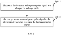
- FIG. 6 illustrates a sub-process of the block 401 of FIG. 5 , according to one embodiment of the disclosure.
- the block 401 may include the flowing steps.
- Block 4011 the electronic device 100 sends a first preset pulse signal to the charger 200 via the charge cable 300.
- the first preset pulse signal is a handshake request signal used to request a handshake for fast charge.
- Block 4012 the charger 200 sends a second preset pulse signal to the electronic device 100 to inform the electronic device 100 that the charger 200 has received the first preset pulse signal, and controls the common terminals T31, T41 of the switches K3, K4 of the connection switching circuit 24 to respectively connect to the normally open terminals T33, T43 of the switches K3, K4 of the connection switching circuit 24. That is, the second preset pulse signal is a handshake confirm signal to inform the electronic device 100 that the charger 200 agrees to the request.
- the second preset pulse signal is a handshake confirm signal to inform the electronic device 100 that the charger 200 agrees to the request.
- the electronic device 100 determines the handshake between the electronic device 100 and the charger 200 is created successfully when receiving the second preset pulse signal, the electronic device 100 then controls the common terminals T11, T21 of the switches K1, K2 of the connection switching circuit 13 to respectively connect to the normally open terminals T13, T23 of the switches K1, K2 of the connection switching circuit 13.
- FIG. 7 illustrates a sub-process of the block 401 of FIG. 5 , according to another embodiment of the disclosure.
- the block 401 may include the flowing steps.
- Block 4013 the electronic device 100 sends a first preset pulse signal to the charger 200 via the charge cable 300.
- the first preset pulse signal is a handshake request signal used to request a handshake for fast charge.
- Block 4014 The charger 200 sends a second preset pulse signal to the electronic device 100 to inform the electronic device 100 that the charger 200 has received the first preset pulse signal and request the electronic device 100 to switch a circuit connection to a fast charge circuit connection. That is, the second preset pulse signal is a handshake confirm signal to inform the electronic device 100 that the charger 200 agrees to the request.
- the second preset pulse signal is a handshake confirm signal to inform the electronic device 100 that the charger 200 agrees to the request.
- Block 4015 the electronic device 100 determines the handshake between the electronic device 100 and the charger 200 is created successfully when receiving the second preset pulse signal, and sends a third preset pulse signal to the controller 23 of the charger 200, and then controls the common terminals T11, T21 of the switches K1, K2 of the connection switching circuit 13 to respectively connect to the normally open terminals T13, T23 of the switches K1, K2 of the connection switching circuit 13.
- the charger 200 determines the handshake between the electronic device 100 and the charger 200 is created successfully when receiving the third preset pulse signal, and controls the common terminals T31, T41 of the switches K3, K4 of the connection switching circuit 24 to respectively connect to the normally open terminals T33, T43 of the switches K3, K4 of the connection switching circuit 24, and enhances the charge power output to the electronic device 100.
- the third preset pulse signal is a charge request signal used to request the charger 200 to prepare charge the electronic device 100.
- the charger 200 may enhance the charge voltage or the charge current provided to the electronic device 100.
Landscapes
- Engineering & Computer Science (AREA)
- Power Engineering (AREA)
- Charge And Discharge Circuits For Batteries Or The Like (AREA)
Claims (15)
- Ladegerät (200), das Folgendes umfasst:einen Ladeport (22), der einen Leistungskontakt (Vbus), einen ersten Datenkontakt (D-), einen zweiten Datenkontakt (D+) und einen Massekontakt (GND) umfasst, wobei der erste Datenkontakt (D-) vom zweiten Datenkontakt (D+) getrennt ist, wobei der Ladeport (22) zum Verbinden mit einem elektronischen Gerät (100) konfiguriert ist;eine Steuerung (23), die mit dem ersten Datenkontakt (D-) und dem zweiten Datenkontakt (D+) verbunden ist;wobei das Ladegerät (200) dadurch gekennzeichnet ist, dass es Folgendes umfasst:einen Verbindungsschaltkreis (24), der mit dem Leistungskontakt (Vbus), dem ersten Datenkontakt (D-), dem zweiten Datenkontakt (D+) und dem Massekontakt (GND) und der Steuerung (23) verbunden ist;wobei die Steuerung (23) zum Steuern des Verbindungsschaltkreises (24) zum Verbinden des ersten Datenkontakts (D-) mit dem Leistungskontakt (Vbus) und zum Verbinden des zweiten Datenkontakts (D+) mit dem Massekontakt (GND) konfiguriert ist, wenn ein Handshake zwischen dem Ladegerät (200) und dem am Ladeport (22) angeschlossenen elektronischen Gerät (100) erfolgreich erzeugt ist.
- Ladegerät (200) nach Anspruch 1, wobei die Steuerung (23) ein Handshake-Anforderungssignal von dem elektronischen Gerät (100) über den ersten Datenkontakt (D-) und/oder den zweiten Datenkontakt (D+) empfängt und ein Handshake-Bestätigungssignal zu dem elektronischen Gerät (100) über den ersten Datenkontakt (D-) und/oder den zweiten Datenkontakt (D+) als Reaktion auf das Handshake-Anforderungssignal sendet; wobei die Steuerung (23) feststellt, dass das Handshake zwischen dem Ladegerät (200) und dem elektronischen Gerät (100) erfolgreich erzeugt ist, wenn sie das Handshake-Anforderungssignal von dem elektronischen Gerät (100) empfängt.
- Ladegerät (200) nach Anspruch 1, wobei die Steuerung (23) ein Handshake-Anforderungssignal von dem elektronischen Gerät (100) über den ersten Datenkontakt (D-) und/oder den zweiten Datenkontakt (D+) empfängt und ein Handshake-Bestätigungssignal sendet, um das elektronische Gerät (100) zu informieren, dass das Ladegerät (200) das Handshake-Anforderungssignal empfangen hat, und um das elektronische Gerät (100) zum Schalten einer Schaltkreisverbindung auf eine schnelle Ladekreisverbindung aufzufordern; die Steuerung (23) feststellt, dass das Handshake zwischen dem Ladegerät (200) und dem elektronischen Gerät (100) erfolgreich erzeugt ist, wenn sie ein Ladeanforderungssignal vom elektronischen Gerät (100) erhält, das Ladeanforderungssignal gesendet wird, wenn das elektronische Gerät (100) das Handshake-Bestätigungssignal vom Ladegerät (200) empfängt.
- Ladegerät (200) nach einem der Ansprüche 1-3, wobei der Verbindungsschaltkreis (24) einen ersten Schalter (K3) und einen zweiten Schalter (K4) umfasst; der erste Schalter (K3) und der zweite Schalter (K4) jeweils eine gemeinsame Klemme (T31/T41), eine Öffnungsklemme (T32/T42) und eine Schließklemme (T33/T43) umfassen; die gemeinsame Klemme (T31) des ersten Schalters (K3) mit dem ersten Datenkontakt (D-) des Ladeports (22) verbunden ist, die Öffnungsklemme (T32) des ersten Schalters (K3) mit der Steuerung (23) verbunden ist und die Schließklemme (T33) des ersten Schalters (K3) mit dem Leistungskontakt (Vbus) des Ladeports (22) verbunden ist; die gemeinsame Klemme (T41) des zweiten Schalters (K4) mit dem zweiten Datenkontakt (D+) des Ladeports (22) verbunden ist, die Öffnungsklemme (T42) des zweiten Schalters (K4) mit der Steuerung (23) verbunden ist und die Schließklemme (T43) des zweiten Schalters (K4) mit dem Massekontakt (GND) des Ladeports (22) verbunden ist; anfänglich die gemeinsamen Klemmen (T31/T41) des ersten Schalters (K3) und des zweiten Schalters (K4) jeweils mit den Öffnungsklemmen (T32/T42) des ersten Schalters (K3) und des zweiten Schalters (K4) verbunden sind; wenn das Handshake zwischen dem Ladegerät (200) und dem elektronischen Gerät (100) erfolgreich erzeugt ist, dann steuert die Steuerung (23) die gemeinsame Klemme (T31) des ersten Schalters (K3) zum Verbinden mit der Schließklemme (T33) des ersten Schalters (K3) und steuert die gemeinsame Klemme (T41) des zweiten Schalters (K4) zum Verbinden mit der Schließklemme (T43) des zweiten Schalters (K4), um so den ersten Datenkontakt (D-) des Ladeports (22) mit dem Leistungskontakt (Vbus) des Ladeports (22) zu verbinden und den zweiten Datenkontakt (D+) des Ladeports (22) mit dem Massekontakt (GND) des Ladeports (22) zu verbinden.
- Ladegerät (200) nach einem der Ansprüche 1-3, wobei die Steuerung (23) ferner zum Unterbrechen der Verbindung zwischen dem ersten Datenkontakt (D-) und dem Leistungskontakt (Vbus) und zum Unterbrechen der Verbindung zwischen dem zweiten Datenkontakt (D+) und dem Massekontakt (GND) konfiguriert ist, wenn der Ladeport (22) und das elektronische Gerät (100) getrennt sind oder das elektronische Gerät (100) voll aufgeladen ist.
- Ladegerät (200) nach Anspruch 1, das ferner eine mit der Steuerung (23) verbundene Leistungsregelschaltung (27) umfasst, wenn das Handshake zwischen dem elektronischen Gerät (100) und dem Ladegerät (200) erfolgreich erzeugt ist, die Steuerung (23) ferner die Leistungsregelschaltung (27) zum Verstärken des Stromausgangs zum kurzgeschlossenen ersten Datenkontakt (D-) und zum Leistungskontakt (Vbus) und zum Verstärken des Stromausgangs zum kurzgeschlossenen zweiten Datenkontakt (D+) und zum Massekontakt (GND) steuert.
- Ladegerät (200) nach Anspruch 1, das ferner einen mit der Steuerung (23) verbundenen Leistungsregelkreis (27) umfasst, wenn das Handshake zwischen dem elektronischen Gerät (100) und dem Ladegerät (200) erfolgreich erzeugt ist, die Steuerung (23) ferner die Leistungsregelschaltung (27) zum Verstärken des Spannungsausgangs zu dem kurzgeschlossenen ersten Datenkontakt (D-) und dem Leistungskontakt (Vbus) und zum Verstärken des Spannungsausgangs zu dem kurzgeschlossenen zweiten Datenkontakt (D+) und dem Massekontakt (GND) steuert.
- Elektronisches Gerät (100), das Folgendes umfasst:einen Leistungsport (11), der einen Leistungskontakt (Vbus), einen ersten Datenkontakt (D-), einen zweiten Datenkontakt (D+) und einen Massekontakt (GND) umfasst, wobei der erste Datenkontakt (D-) vom zweiten Datenkontakt (D+) getrennt ist, wobei der Leistungsport (11) zum Verbinden mit einem Ladegerät (200) konfiguriert ist;einen Prozessor (12), der mit dem ersten Datenkontakt (D-) und dem zweiten Datenkontakt (D+) verbunden ist;wobei das elektronische Gerät (100) dadurch gekennzeichnet ist, dass es ferner Folgendes umfasst:einen Verbindungsschaltkreis (13), der mit dem Leistungskontakt (Vbus), dem ersten Datenkontakt (D-), dem zweiten Datenkontakt (D+) und dem Massekontakt (GND) und dem Prozessor (12) verbunden ist;wobei der Prozessor (12) konfiguriert ist zum Einleiten eines Handshake zwischen dem elektronischen Gerät (100) und dem Ladegerät (200), wenn der Leistungsport (11) mit einem Ladeport (22) des Ladegeräts (200) verbunden ist, und zum Steuern des Verbindungsschaltkreises (13) zum Verbinden des ersten Datenkontakts (D-) mit dem Leistungskontakt (Vbus) und zum Verbinden des zweiten Datenkontakts (D+) mit dem Massekontakt (GND), wenn das Handshake zwischen dem elektronischen Gerät (100) und dem Ladegerät (200) erfolgreich erzeugt ist.
- Elektronisches Gerät (100) nach Anspruch 8, wobei der Verbindungsschaltkreis (13) einen ersten Schalter (K1) und einen zweiten Schalter (K2) umfasst; der erste Schalter (K1) und der zweite Schalter (K2) jeweils eine gemeinsame Klemme (T11/T21), eine Öffnungsklemme (T12/T22) und eine Schließklemme (T13/T23) umfassen; die gemeinsame Klemme (T11) des ersten Schalters (K1) mit dem ersten Datenkontakt (D-) des Leistungsports (11) verbunden ist, die Öffnungsklemme (T12) des ersten Schalters (K1) mit dem Prozessor (12) verbunden ist und die Schließklemme (T13) des ersten Schalters (K1) mit dem Leistungskontakt (Vbus) des Leistungsports (11) verbunden ist; die gemeinsame Klemme (T21) des zweiten Schalters (K2) mit dem zweiten Datenkontakt (D+) des Leistungsports (11) verbunden ist, die Öffnungsklemme (T22) des zweiten Schalters (K2) mit dem Prozessor (12) verbunden ist und die Schließklemme (T23) des zweiten Schalters (K2) mit dem Massekontakt (GND) des Leistungsports (11) verbunden ist; anfänglich die gemeinsamen Klemmen (T11/T21) des ersten Schalters (K1) und des zweiten Schalters (K2) jeweils mit den Öffnungsklemmen (T12/T22) des ersten Schalters (K1) und des zweiten Schalters (K2) verbunden sind; wenn das Handshake zwischen dem elektronischen Gerät (100) und dem Ladegerät (200) erfolgreich erzeugt ist, dann steuert der Prozessor (12) die gemeinsame Klemme (T11) des ersten Schalters (K1) zum Verbinden mit der Schließklemme (T13) des ersten Schalters (K1) und steuert die gemeinsame Klemme (T21) des zweiten Schalters (K2) zum Verbinden mit der Schließklemme (T23) des zweiten Schalters (K2), um so den ersten Datenkontakt (D-) des Leistungsports (11) mit dem Leistungskontakt (Vbus) des Leistungsports (11) zu verbinden und den zweiten Datenkontakt (D+) des Leistungsports (11) mit dem Massekontakt (GND) des Leistungsports (11) zu verbinden.
- Elektronisches Gerät (100) nach Anspruch 8, wobei der Prozessor (12) ferner einen dritten Datenkontakt (D-) des Ladeports (22) zum Verbinden mit einem zweiten Leistungskontakt (Vbus) des Ladeports (22) auslöst und einen vierten Datenkontakt (D+) des Ladeports (22) zum Verbinden mit einem zweiten Massekontakt (GND) des Ladeports (22) auslöst, wenn das Handshake zwischen dem elektronischen Gerät (100) und dem Ladegerät (200) erfolgreich erzeugt ist.
- Elektronisches Gerät (100) nach einem der Ansprüche 8-10, wobei der Prozessor (12) das Handshake zwischen dem elektronischen Gerät (100) und dem Ladegerät (200) wie folgt einleitet: der Prozessor (12) sendet ein Handshake-Anforderungssignal zum Ladegerät (200) über den ersten Datenkontakt (D-) und/oder den zweiten Datenkontakt (D+) und empfängt ein Handshake-Bestätigungssignal, zurückgesendet vom Ladegerät (200), das auf das Handshake-Anforderungssignal antwortet, über den ersten Datenkontakt (D-) und/oder den zweiten Datenkontakt (D+); der Prozessor (12) stellt fest, dass das Handshake zwischen dem elektronischen Gerät (100) und dem Ladegerät (200) erfolgreich erzeugt ist, wenn er das Handshake-Bestätigungssignal empfängt.
- Elektronisches Gerät (100) nach Anspruch 11, wobei der Prozessor (12) ferner eine Ladeanforderung zum Ladegerät (200) sendet, wenn er das Handshake-Bestätigungssignal empfängt, um das Ladegerät (200) zu informieren, einen dritten Datenkontakt (D-) des Ladegeräts (200) mit dem Leistungskontakt (Vbus) des Ladegeräts (200) zu verbinden und den vierten Datenkontakt (D+) des Ladegeräts (200) mit dem Massekontakt (GND) des Ladegeräts (200) zu verbinden.
- Elektronisches Gerät (100) nach Anspruch 11, wobei das elektronische Gerät (100) ferner eine Lademanagementeinheit (14) und eine Batterie (15) umfasst, die Lademanagementeinheit (14) mit dem Leistungsport (11) und der Batterie (15) verbunden ist, und konfiguriert ist zum Empfangen von Leistungsenergie, die das Ladegerät (200) vom Leistungsport (11) bereitstellt, und zum Umwandeln der Leistungsenergie in eine geeignete Ladespannung oder einen geeigneten Ladestrom zum Laden der Batterie (15).
- Elektronisches Gerät (100) nach Anspruch 13, wobei die Lademanagementeinheit (14) eine erste Lademanagementeinheit (141) und eine zweite Lademanagementeinheit (142) umfasst, wobei die erste Lademanagementeinheit (141) und die zweite Lademanagementeinheit (142) beide mit dem Leistungskontakt (Vbus) und dem Massekontakt (GND) des Leistungsports (11) verbunden sind, ein vom Leistungskontakt (Vbus) und vom Massekontakt (GND) empfangener Eingangsstrom zu zwei Shuntströmen geschaltet werden, und die zwei Shuntströme jeweils zur ersten Lademanagementeinheit (141) und zur zweiten Lademanagementeinheit (142) übertragen werden; die erste Lademanagementeinheit (141) und die zweite Lademanagementeinheit (142) beide mit der Batterie (15) verbunden sind, und von der ersten Lademanagementeinheit (141) und der zweiten Lademanagementeinheit (142) ausgegebene Ausgangsströme zu einem gemeinsamen Strom zum Laden der Batterie (15) kombiniert werden.
- Ladeverfahren, konfiguriert zum Laden eines elektronischen Geräts (100) mittels eines Ladegeräts (200), wobei das Ladeverfahren Folgendes beinhaltet:Einleiten eines Handshake zwischen dem elektronischen Gerät (100) und dem Ladegerät (200), wenn das elektronische Gerät (100) über ein Ladekabel (300) mit dem Ladegerät (200) verbunden ist;wobei das Ladeverfahren dadurch gekennzeichnet ist, dass es ferner Folgendes beinhaltet:Steuern eines ersten Datenkontakts (D-) eines Leistungsports (11) des elektronischen Geräts (100) zum Verbinden mit einem ersten Leistungskontakt (Vbus) des Leistungsports (11) des elektronischen Geräts (100) und zum Steuern eines zweiten Datenkontakts (D+) des Leistungsports (11) des elektronischen Geräts (100) zum Verbinden mit einem ersten Massekontakt (GND) des Leistungsports (11) des elektronischen Geräts (100), wenn das Handshake zwischen dem elektronischen Gerät (100) und dem Ladegerät (200) erfolgreich erzeugt ist; undSteuern eines dritten Datenkontakts (D-) eines Ladeports (22) des Ladegeräts (200) zum Verbinden mit einem zweiten Leistungskontakt (Vbus) des Ladeports (22) des Ladegeräts (200) und Steuern eines vierten Datenkontakts (D+) des Ladeports (22) des Ladegeräts (200) zum Verbinden mit einem zweiten Massekontakt (GND) des Ladeports (22) des Ladegeräts (200), wenn das Handshake zwischen dem elektronischen Gerät (100) und dem Ladegerät (200) erfolgreich erzeugt ist, wobei der Datenkontakt (D-) immer vom vierten Datenkontakt (D+) getrennt ist.
Applications Claiming Priority (2)
| Application Number | Priority Date | Filing Date | Title |
|---|---|---|---|
| PCT/CN2016/096043 WO2018032503A1 (zh) | 2016-08-19 | 2016-08-19 | 一种电源适配器、终端设备、充电系统及充电方法 |
| PCT/CN2016/106600 WO2018090371A1 (zh) | 2016-11-21 | 2016-11-21 | 电子装置、充电器、充电系统及充电方法 |
Publications (2)
| Publication Number | Publication Date |
|---|---|
| EP3285356A1 EP3285356A1 (de) | 2018-02-21 |
| EP3285356B1 true EP3285356B1 (de) | 2019-02-20 |
Family
ID=59686769
Family Applications (1)
| Application Number | Title | Priority Date | Filing Date |
|---|---|---|---|
| EP17186821.9A Not-in-force EP3285356B1 (de) | 2016-08-19 | 2017-08-18 | Ladevorrichtung, elektronische vorrichtung und ladeverfahren |
Country Status (3)
| Country | Link |
|---|---|
| US (1) | US10461556B2 (de) |
| EP (1) | EP3285356B1 (de) |
| CN (2) | CN207398851U (de) |
Families Citing this family (20)
| Publication number | Priority date | Publication date | Assignee | Title |
|---|---|---|---|---|
| SG11201700500WA (en) * | 2015-09-22 | 2017-04-27 | Guangdong Oppo Mobile Telecomm | Charge control method and device, and electronic device |
| JP6838879B2 (ja) * | 2016-07-13 | 2021-03-03 | ローム株式会社 | 受電装置およびその制御回路、電子機器、給電システムの動作方法 |
| CN207398851U (zh) * | 2016-08-19 | 2018-05-22 | 深圳市柔宇科技有限公司 | 充电器、电子装置及充电系统 |
| CN111201690A (zh) * | 2017-12-11 | 2020-05-26 | 深圳市柔宇科技有限公司 | 充电控制方法、电子装置、电源适配器及充电控制系统 |
| TWI673612B (zh) * | 2018-08-07 | 2019-10-01 | 技嘉科技股份有限公司 | 具有充電功能的主機板 |
| TWI662764B (zh) | 2018-08-07 | 2019-06-11 | 技嘉科技股份有限公司 | 具有智能充電功能的主機板 |
| WO2020073231A1 (zh) * | 2018-10-10 | 2020-04-16 | 深圳市柔宇科技有限公司 | 一种goa电路及显示装置 |
| CN110021981B (zh) * | 2019-04-30 | 2021-03-23 | 维沃移动通信有限公司 | 充电器及终端 |
| CN110289663B (zh) * | 2019-07-30 | 2021-02-23 | Oppo(重庆)智能科技有限公司 | 一种终端设备及其电源电路和电源适配器 |
| EP3979454B1 (de) | 2019-08-29 | 2023-04-19 | Guangdong Oppo Mobile Telecommunications Corp., Ltd. | Aufladbare vorrichtung und ladeverfahren |
| CN111030219B (zh) * | 2019-12-13 | 2021-09-17 | 深圳市普威技术有限公司 | 一种可实时通信的快充数据线 |
| CN113364072A (zh) * | 2020-03-06 | 2021-09-07 | 华为技术有限公司 | 一种充电方法、设备和系统 |
| CN112994161A (zh) * | 2020-05-28 | 2021-06-18 | 上海闻泰电子科技有限公司 | 终端和充电器 |
| CN111509818B (zh) * | 2020-05-29 | 2022-06-24 | 维沃移动通信有限公司 | 充电器、数据线和充电设备 |
| CN111817382B (zh) * | 2020-07-14 | 2022-02-08 | 维沃移动通信有限公司 | 充电器、数据线和充电设备 |
| US12212162B2 (en) * | 2020-07-15 | 2025-01-28 | Huawei Technologies Co., Ltd. | Charging cable-based data transmission method and electronic device |
| CN112086830B (zh) * | 2020-07-23 | 2022-12-06 | 福建联迪商用设备有限公司 | 一种与iOS设备通信的数据线电路 |
| CN111864864B (zh) * | 2020-08-21 | 2025-01-17 | 上海木木聚枞机器人科技有限公司 | 一种自动回充方法及系统 |
| US20230361592A1 (en) * | 2020-11-26 | 2023-11-09 | Annvolt Technology Co., Ltd. | Charger and charging system |
| CN114759809A (zh) * | 2022-05-10 | 2022-07-15 | 昂宝电子(上海)有限公司 | 开关电源和用在开关电源中的方法 |
Family Cites Families (18)
| Publication number | Priority date | Publication date | Assignee | Title |
|---|---|---|---|---|
| US8386814B2 (en) | 2009-07-20 | 2013-02-26 | Texas Instruments Incorporated | Continuous monitoring of a USB client for battery charging specification charging capacity |
| CN102393837B (zh) | 2011-11-08 | 2014-07-30 | 深圳市海思半导体有限公司 | 一种usb充电器识别装置及方法 |
| JP2013102625A (ja) | 2011-11-09 | 2013-05-23 | Sony Corp | 充電制御装置及び充電制御方法 |
| CN102684270B (zh) | 2012-05-31 | 2014-12-10 | 华为技术有限公司 | 一种识别usb充电器类型的方法及usb设备 |
| JP5986026B2 (ja) * | 2013-03-21 | 2016-09-06 | ルネサスエレクトロニクス株式会社 | ホスト装置、ホスト装置の制御方法及び半導体装置 |
| CN203747451U (zh) | 2014-01-28 | 2014-07-30 | 广东欧珀移动通信有限公司 | 电池充电装置 |
| CN105022468B (zh) * | 2014-04-21 | 2018-06-01 | 国基电子(上海)有限公司 | Usb适配器及usb线 |
| CN104124732A (zh) * | 2014-06-27 | 2014-10-29 | 青岛众海汇智能源科技有限责任公司 | 基于usb接口的移动终端通用无线供电电路及其供电方法 |
| JP5986145B2 (ja) | 2014-07-02 | 2016-09-06 | レノボ・シンガポール・プライベート・リミテッド | ポータブル・デバイス、ケーブル・アセンブリおよびusbシステム |
| EP3159999B1 (de) * | 2014-07-16 | 2019-01-16 | Huawei Technologies Co., Ltd. | Verfahren, einrichtung und vorrichtung zum schnellladen einer elektronischen vorrichtung |
| CN104393628B (zh) * | 2014-08-29 | 2017-02-01 | 展讯通信(上海)有限公司 | Usb充电器、移动终端和充电控制方法 |
| CN104300628A (zh) | 2014-10-17 | 2015-01-21 | 无锡中星微电子有限公司 | 借用智能设备显示移动电源信息的移动电源及方法 |
| MY176505A (en) * | 2014-11-11 | 2020-08-12 | Guangdong Oppo Mobile Telecommunications Corp Ltd | Power adapter and terminal |
| KR101898185B1 (ko) * | 2014-11-11 | 2018-09-12 | 광동 오포 모바일 텔레커뮤니케이션즈 코포레이션 리미티드 | 전원 어댑터, 단말기 및 충전 시스템 |
| CN104506055B (zh) | 2014-12-26 | 2018-07-06 | 东莞市时瑞电池有限公司 | 自适应电压输出电源电路及电源装置 |
| CN105098900B (zh) * | 2015-08-05 | 2018-05-29 | 青岛海信移动通信技术股份有限公司 | 移动终端、可直充电源适配器及充电方法 |
| CN106058983B (zh) | 2016-06-30 | 2019-01-29 | 维沃移动通信有限公司 | 一种充电控制电路、电子设备,及充电控制方法 |
| CN207398851U (zh) * | 2016-08-19 | 2018-05-22 | 深圳市柔宇科技有限公司 | 充电器、电子装置及充电系统 |
-
2017
- 2017-08-18 CN CN201721035898.1U patent/CN207398851U/zh active Active
- 2017-08-18 EP EP17186821.9A patent/EP3285356B1/de not_active Not-in-force
- 2017-08-18 US US15/680,340 patent/US10461556B2/en not_active Expired - Fee Related
- 2017-08-18 CN CN201710710224.5A patent/CN107359668A/zh active Pending
Non-Patent Citations (1)
| Title |
|---|
| None * |
Also Published As
| Publication number | Publication date |
|---|---|
| US20180054074A1 (en) | 2018-02-22 |
| US10461556B2 (en) | 2019-10-29 |
| EP3285356A1 (de) | 2018-02-21 |
| CN207398851U (zh) | 2018-05-22 |
| CN107359668A (zh) | 2017-11-17 |
Similar Documents
| Publication | Publication Date | Title |
|---|---|---|
| EP3285356B1 (de) | Ladevorrichtung, elektronische vorrichtung und ladeverfahren | |
| US20190109484A1 (en) | Electronic device, charger, and charging method | |
| US8386814B2 (en) | Continuous monitoring of a USB client for battery charging specification charging capacity | |
| US11451077B2 (en) | Electronic equipment, charger and charging method | |
| CN105576727B (zh) | 一种快速充电的方法、装置和系统 | |
| KR101474097B1 (ko) | 케이블 내의 전력 분배 | |
| EP2854253B1 (de) | Ladegerät, Ladeendgerät, Ladesystem und Steuerverfahren zum Laden | |
| US20180254650A1 (en) | Methods, electronic devices, and charger apparatus for quick usb charging | |
| CN104065147B (zh) | 一种充电适配器、终端、充电控制方法 | |
| CN105140583B (zh) | 基于usb端口的快速充电方法 | |
| EP3086433A1 (de) | Ladeverfahren, wechselstromadapter, lademanagementvorrichtung und endvorrichtung | |
| EP3032693B1 (de) | Elektronische vorrichtung und netzadapter mit fähigkeit zur kommunikation miteinander und zugehöriges ladesystem | |
| CN111049214A (zh) | 一种充电方法、终端及充电适配器 | |
| CN105471008A (zh) | 一种信息处理方法、第一电子设备和第二电子设备 | |
| CN110492575B (zh) | 用于手持设备的快速充电系统及方法、手持设备 | |
| US20150349561A1 (en) | Charging an electrical device via a data interface | |
| CN106249830B (zh) | 电能传输系统及方法 | |
| JP2016218972A (ja) | Usbハブ装置 | |
| JP3796419B2 (ja) | 端末装置 | |
| KR20180033452A (ko) | 전력 어댑터, 단말기 장치, 충전 시스템 및 충전 방법 | |
| CN109861038B (zh) | 可自动切换连接模式的usb连接埠及其控制方法 | |
| CN108336791B (zh) | 充电控制方法以及电子设备 | |
| CN107492921B (zh) | 电子装置及其充电控制电路 | |
| CN118842138A (zh) | 一种支持双向盲插的多功能充电装置 | |
| CN204886334U (zh) | 充电识别电路及充电识别芯片 |
Legal Events
| Date | Code | Title | Description |
|---|---|---|---|
| PUAI | Public reference made under article 153(3) epc to a published international application that has entered the european phase |
Free format text: ORIGINAL CODE: 0009012 |
|
| STAA | Information on the status of an ep patent application or granted ep patent |
Free format text: STATUS: REQUEST FOR EXAMINATION WAS MADE |
|
| 17P | Request for examination filed |
Effective date: 20170818 |
|
| AK | Designated contracting states |
Kind code of ref document: A1 Designated state(s): AL AT BE BG CH CY CZ DE DK EE ES FI FR GB GR HR HU IE IS IT LI LT LU LV MC MK MT NL NO PL PT RO RS SE SI SK SM TR |
|
| AX | Request for extension of the european patent |
Extension state: BA ME |
|
| GRAP | Despatch of communication of intention to grant a patent |
Free format text: ORIGINAL CODE: EPIDOSNIGR1 |
|
| STAA | Information on the status of an ep patent application or granted ep patent |
Free format text: STATUS: GRANT OF PATENT IS INTENDED |
|
| INTG | Intention to grant announced |
Effective date: 20180904 |
|
| GRAS | Grant fee paid |
Free format text: ORIGINAL CODE: EPIDOSNIGR3 |
|
| GRAA | (expected) grant |
Free format text: ORIGINAL CODE: 0009210 |
|
| STAA | Information on the status of an ep patent application or granted ep patent |
Free format text: STATUS: THE PATENT HAS BEEN GRANTED |
|
| AK | Designated contracting states |
Kind code of ref document: B1 Designated state(s): AL AT BE BG CH CY CZ DE DK EE ES FI FR GB GR HR HU IE IS IT LI LT LU LV MC MK MT NL NO PL PT RO RS SE SI SK SM TR |
|
| REG | Reference to a national code |
Ref country code: GB Ref legal event code: FG4D |
|
| REG | Reference to a national code |
Ref country code: CH Ref legal event code: EP |
|
| REG | Reference to a national code |
Ref country code: DE Ref legal event code: R096 Ref document number: 602017002220 Country of ref document: DE |
|
| REG | Reference to a national code |
Ref country code: AT Ref legal event code: REF Ref document number: 1099445 Country of ref document: AT Kind code of ref document: T Effective date: 20190315 |
|
| REG | Reference to a national code |
Ref country code: IE Ref legal event code: FG4D |
|
| REG | Reference to a national code |
Ref country code: LT Ref legal event code: MG4D Ref country code: NL Ref legal event code: MP Effective date: 20190220 |
|
| PG25 | Lapsed in a contracting state [announced via postgrant information from national office to epo] |
Ref country code: NO Free format text: LAPSE BECAUSE OF FAILURE TO SUBMIT A TRANSLATION OF THE DESCRIPTION OR TO PAY THE FEE WITHIN THE PRESCRIBED TIME-LIMIT Effective date: 20190520 Ref country code: FI Free format text: LAPSE BECAUSE OF FAILURE TO SUBMIT A TRANSLATION OF THE DESCRIPTION OR TO PAY THE FEE WITHIN THE PRESCRIBED TIME-LIMIT Effective date: 20190220 Ref country code: PT Free format text: LAPSE BECAUSE OF FAILURE TO SUBMIT A TRANSLATION OF THE DESCRIPTION OR TO PAY THE FEE WITHIN THE PRESCRIBED TIME-LIMIT Effective date: 20190620 Ref country code: LT Free format text: LAPSE BECAUSE OF FAILURE TO SUBMIT A TRANSLATION OF THE DESCRIPTION OR TO PAY THE FEE WITHIN THE PRESCRIBED TIME-LIMIT Effective date: 20190220 Ref country code: SE Free format text: LAPSE BECAUSE OF FAILURE TO SUBMIT A TRANSLATION OF THE DESCRIPTION OR TO PAY THE FEE WITHIN THE PRESCRIBED TIME-LIMIT Effective date: 20190220 |
|
| PG25 | Lapsed in a contracting state [announced via postgrant information from national office to epo] |
Ref country code: BG Free format text: LAPSE BECAUSE OF FAILURE TO SUBMIT A TRANSLATION OF THE DESCRIPTION OR TO PAY THE FEE WITHIN THE PRESCRIBED TIME-LIMIT Effective date: 20190520 Ref country code: GR Free format text: LAPSE BECAUSE OF FAILURE TO SUBMIT A TRANSLATION OF THE DESCRIPTION OR TO PAY THE FEE WITHIN THE PRESCRIBED TIME-LIMIT Effective date: 20190521 Ref country code: RS Free format text: LAPSE BECAUSE OF FAILURE TO SUBMIT A TRANSLATION OF THE DESCRIPTION OR TO PAY THE FEE WITHIN THE PRESCRIBED TIME-LIMIT Effective date: 20190220 Ref country code: IS Free format text: LAPSE BECAUSE OF FAILURE TO SUBMIT A TRANSLATION OF THE DESCRIPTION OR TO PAY THE FEE WITHIN THE PRESCRIBED TIME-LIMIT Effective date: 20190620 Ref country code: LV Free format text: LAPSE BECAUSE OF FAILURE TO SUBMIT A TRANSLATION OF THE DESCRIPTION OR TO PAY THE FEE WITHIN THE PRESCRIBED TIME-LIMIT Effective date: 20190220 Ref country code: HR Free format text: LAPSE BECAUSE OF FAILURE TO SUBMIT A TRANSLATION OF THE DESCRIPTION OR TO PAY THE FEE WITHIN THE PRESCRIBED TIME-LIMIT Effective date: 20190220 Ref country code: NL Free format text: LAPSE BECAUSE OF FAILURE TO SUBMIT A TRANSLATION OF THE DESCRIPTION OR TO PAY THE FEE WITHIN THE PRESCRIBED TIME-LIMIT Effective date: 20190220 |
|
| REG | Reference to a national code |
Ref country code: AT Ref legal event code: MK05 Ref document number: 1099445 Country of ref document: AT Kind code of ref document: T Effective date: 20190220 |
|
| PG25 | Lapsed in a contracting state [announced via postgrant information from national office to epo] |
Ref country code: RO Free format text: LAPSE BECAUSE OF FAILURE TO SUBMIT A TRANSLATION OF THE DESCRIPTION OR TO PAY THE FEE WITHIN THE PRESCRIBED TIME-LIMIT Effective date: 20190220 Ref country code: IT Free format text: LAPSE BECAUSE OF FAILURE TO SUBMIT A TRANSLATION OF THE DESCRIPTION OR TO PAY THE FEE WITHIN THE PRESCRIBED TIME-LIMIT Effective date: 20190220 Ref country code: SK Free format text: LAPSE BECAUSE OF FAILURE TO SUBMIT A TRANSLATION OF THE DESCRIPTION OR TO PAY THE FEE WITHIN THE PRESCRIBED TIME-LIMIT Effective date: 20190220 Ref country code: CZ Free format text: LAPSE BECAUSE OF FAILURE TO SUBMIT A TRANSLATION OF THE DESCRIPTION OR TO PAY THE FEE WITHIN THE PRESCRIBED TIME-LIMIT Effective date: 20190220 Ref country code: AL Free format text: LAPSE BECAUSE OF FAILURE TO SUBMIT A TRANSLATION OF THE DESCRIPTION OR TO PAY THE FEE WITHIN THE PRESCRIBED TIME-LIMIT Effective date: 20190220 Ref country code: DK Free format text: LAPSE BECAUSE OF FAILURE TO SUBMIT A TRANSLATION OF THE DESCRIPTION OR TO PAY THE FEE WITHIN THE PRESCRIBED TIME-LIMIT Effective date: 20190220 Ref country code: ES Free format text: LAPSE BECAUSE OF FAILURE TO SUBMIT A TRANSLATION OF THE DESCRIPTION OR TO PAY THE FEE WITHIN THE PRESCRIBED TIME-LIMIT Effective date: 20190220 Ref country code: EE Free format text: LAPSE BECAUSE OF FAILURE TO SUBMIT A TRANSLATION OF THE DESCRIPTION OR TO PAY THE FEE WITHIN THE PRESCRIBED TIME-LIMIT Effective date: 20190220 |
|
| PGFP | Annual fee paid to national office [announced via postgrant information from national office to epo] |
Ref country code: FR Payment date: 20190830 Year of fee payment: 3 Ref country code: DE Payment date: 20190807 Year of fee payment: 3 |
|
| REG | Reference to a national code |
Ref country code: DE Ref legal event code: R097 Ref document number: 602017002220 Country of ref document: DE |
|
| PG25 | Lapsed in a contracting state [announced via postgrant information from national office to epo] |
Ref country code: PL Free format text: LAPSE BECAUSE OF FAILURE TO SUBMIT A TRANSLATION OF THE DESCRIPTION OR TO PAY THE FEE WITHIN THE PRESCRIBED TIME-LIMIT Effective date: 20190220 Ref country code: SM Free format text: LAPSE BECAUSE OF FAILURE TO SUBMIT A TRANSLATION OF THE DESCRIPTION OR TO PAY THE FEE WITHIN THE PRESCRIBED TIME-LIMIT Effective date: 20190220 |
|
| PLBE | No opposition filed within time limit |
Free format text: ORIGINAL CODE: 0009261 |
|
| STAA | Information on the status of an ep patent application or granted ep patent |
Free format text: STATUS: NO OPPOSITION FILED WITHIN TIME LIMIT |
|
| PG25 | Lapsed in a contracting state [announced via postgrant information from national office to epo] |
Ref country code: AT Free format text: LAPSE BECAUSE OF FAILURE TO SUBMIT A TRANSLATION OF THE DESCRIPTION OR TO PAY THE FEE WITHIN THE PRESCRIBED TIME-LIMIT Effective date: 20190220 |
|
| 26N | No opposition filed |
Effective date: 20191121 |
|
| PG25 | Lapsed in a contracting state [announced via postgrant information from national office to epo] |
Ref country code: SI Free format text: LAPSE BECAUSE OF FAILURE TO SUBMIT A TRANSLATION OF THE DESCRIPTION OR TO PAY THE FEE WITHIN THE PRESCRIBED TIME-LIMIT Effective date: 20190220 |
|
| PG25 | Lapsed in a contracting state [announced via postgrant information from national office to epo] |
Ref country code: TR Free format text: LAPSE BECAUSE OF FAILURE TO SUBMIT A TRANSLATION OF THE DESCRIPTION OR TO PAY THE FEE WITHIN THE PRESCRIBED TIME-LIMIT Effective date: 20190220 |
|
| PG25 | Lapsed in a contracting state [announced via postgrant information from national office to epo] |
Ref country code: LU Free format text: LAPSE BECAUSE OF NON-PAYMENT OF DUE FEES Effective date: 20190818 Ref country code: MC Free format text: LAPSE BECAUSE OF FAILURE TO SUBMIT A TRANSLATION OF THE DESCRIPTION OR TO PAY THE FEE WITHIN THE PRESCRIBED TIME-LIMIT Effective date: 20190220 |
|
| REG | Reference to a national code |
Ref country code: BE Ref legal event code: MM Effective date: 20190831 |
|
| PG25 | Lapsed in a contracting state [announced via postgrant information from national office to epo] |
Ref country code: IE Free format text: LAPSE BECAUSE OF NON-PAYMENT OF DUE FEES Effective date: 20190818 |
|
| PG25 | Lapsed in a contracting state [announced via postgrant information from national office to epo] |
Ref country code: BE Free format text: LAPSE BECAUSE OF NON-PAYMENT OF DUE FEES Effective date: 20190831 |
|
| REG | Reference to a national code |
Ref country code: DE Ref legal event code: R119 Ref document number: 602017002220 Country of ref document: DE |
|
| REG | Reference to a national code |
Ref country code: CH Ref legal event code: PL |
|
| PG25 | Lapsed in a contracting state [announced via postgrant information from national office to epo] |
Ref country code: LI Free format text: LAPSE BECAUSE OF NON-PAYMENT OF DUE FEES Effective date: 20200831 Ref country code: CH Free format text: LAPSE BECAUSE OF NON-PAYMENT OF DUE FEES Effective date: 20200831 |
|
| PG25 | Lapsed in a contracting state [announced via postgrant information from national office to epo] |
Ref country code: CY Free format text: LAPSE BECAUSE OF FAILURE TO SUBMIT A TRANSLATION OF THE DESCRIPTION OR TO PAY THE FEE WITHIN THE PRESCRIBED TIME-LIMIT Effective date: 20190220 |
|
| PG25 | Lapsed in a contracting state [announced via postgrant information from national office to epo] |
Ref country code: DE Free format text: LAPSE BECAUSE OF NON-PAYMENT OF DUE FEES Effective date: 20210302 Ref country code: FR Free format text: LAPSE BECAUSE OF NON-PAYMENT OF DUE FEES Effective date: 20200831 Ref country code: HU Free format text: LAPSE BECAUSE OF FAILURE TO SUBMIT A TRANSLATION OF THE DESCRIPTION OR TO PAY THE FEE WITHIN THE PRESCRIBED TIME-LIMIT; INVALID AB INITIO Effective date: 20170818 Ref country code: MT Free format text: LAPSE BECAUSE OF FAILURE TO SUBMIT A TRANSLATION OF THE DESCRIPTION OR TO PAY THE FEE WITHIN THE PRESCRIBED TIME-LIMIT Effective date: 20190220 |
|
| GBPC | Gb: european patent ceased through non-payment of renewal fee |
Effective date: 20210818 |
|
| PG25 | Lapsed in a contracting state [announced via postgrant information from national office to epo] |
Ref country code: MK Free format text: LAPSE BECAUSE OF FAILURE TO SUBMIT A TRANSLATION OF THE DESCRIPTION OR TO PAY THE FEE WITHIN THE PRESCRIBED TIME-LIMIT Effective date: 20190220 |
|
| PG25 | Lapsed in a contracting state [announced via postgrant information from national office to epo] |
Ref country code: GB Free format text: LAPSE BECAUSE OF NON-PAYMENT OF DUE FEES Effective date: 20210818 |