EP3285404A2 - Digital-zentrische vollduplex-architektur - Google Patents
Digital-zentrische vollduplex-architektur Download PDFInfo
- Publication number
- EP3285404A2 EP3285404A2 EP17173593.9A EP17173593A EP3285404A2 EP 3285404 A2 EP3285404 A2 EP 3285404A2 EP 17173593 A EP17173593 A EP 17173593A EP 3285404 A2 EP3285404 A2 EP 3285404A2
- Authority
- EP
- European Patent Office
- Prior art keywords
- signal
- analog
- circuit
- digital
- full
- Prior art date
- Legal status (The legal status is an assumption and is not a legal conclusion. Google has not performed a legal analysis and makes no representation as to the accuracy of the status listed.)
- Granted
Links
Images





Classifications
-
- H—ELECTRICITY
- H04—ELECTRIC COMMUNICATION TECHNIQUE
- H04B—TRANSMISSION
- H04B1/00—Details of transmission systems, not covered by a single one of groups H04B3/00 - H04B13/00; Details of transmission systems not characterised by the medium used for transmission
- H04B1/06—Receivers
- H04B1/10—Means associated with receiver for limiting or suppressing noise or interference
- H04B1/12—Neutralising, balancing, or compensation arrangements
- H04B1/123—Neutralising, balancing, or compensation arrangements using adaptive balancing or compensation means
-
- H—ELECTRICITY
- H04—ELECTRIC COMMUNICATION TECHNIQUE
- H04L—TRANSMISSION OF DIGITAL INFORMATION, e.g. TELEGRAPHIC COMMUNICATION
- H04L5/00—Arrangements affording multiple use of the transmission path
- H04L5/14—Two-way operation using the same type of signal, i.e. duplex
- H04L5/1461—Suppression of signals in the return path, i.e. bidirectional control circuits
-
- H—ELECTRICITY
- H04—ELECTRIC COMMUNICATION TECHNIQUE
- H04B—TRANSMISSION
- H04B1/00—Details of transmission systems, not covered by a single one of groups H04B3/00 - H04B13/00; Details of transmission systems not characterised by the medium used for transmission
- H04B1/38—Transceivers, i.e. devices in which transmitter and receiver form a structural unit and in which at least one part is used for functions of transmitting and receiving
- H04B1/40—Circuits
- H04B1/44—Transmit/receive switching
-
- H—ELECTRICITY
- H04—ELECTRIC COMMUNICATION TECHNIQUE
- H04B—TRANSMISSION
- H04B1/00—Details of transmission systems, not covered by a single one of groups H04B3/00 - H04B13/00; Details of transmission systems not characterised by the medium used for transmission
- H04B1/38—Transceivers, i.e. devices in which transmitter and receiver form a structural unit and in which at least one part is used for functions of transmitting and receiving
- H04B1/40—Circuits
- H04B1/50—Circuits using different frequencies for the two directions of communication
- H04B1/52—Hybrid arrangements, i.e. arrangements for transition from single-path two-direction transmission to single-direction transmission on each of two paths or vice versa
- H04B1/525—Hybrid arrangements, i.e. arrangements for transition from single-path two-direction transmission to single-direction transmission on each of two paths or vice versa with means for reducing leakage of transmitter signal into the receiver
Definitions
- the disclosure relates to the field of wireless communications, including full-duplex architectures.
- Wireless communication has become ubiquitous in modem society.
- Wireless radios may be designed to operate in half-duplex mode, where the half-duplex radio may transmit or receive on the same frequency band (also referred to as channel), but not both simultaneously.
- In-band full-duplex radios may concurrently transmit and receive signals in the same frequency band.
- In-band full-duplex radios have tremendous implications on wireless network design, not the least of which is cutting spectrum requirements in half.
- LTE Long-Term Evolution
- An in-band full-duplex radio would be able to achieve the same performance using a single channel as a radio implementing LTE.
- In-band full-duplex may be referred to as full-duplex hereinafter, unless otherwise described.
- full-duplex radios also referred to as full-duplex systems, full-duplex radio systems, or full-duplex radio devices
- FDD frequency-division duplex
- Full-duplex radios generate self-interference signals (also referred to as self-interference) that may limit performance.
- TX transmission
- RX receiver
- the self-interference signal acts as unwanted noise and reduces the signal-to-noise ratio (SNR) and throughput of the full-duplex radio.
- SNR signal-to-noise ratio
- Cancellation of self-interference to the noise floor of the full-duplex radio is desirable, but difficult.
- the noise floor may refer to the level of noise introduced by a system (or the level of background noise in a signal), below which the signal that is being captured cannot be isolated from the noise.
- the transmitted analog TX signal may look very different from its digital representation in baseband (also referred to as digital TX baseband signal).
- Baseband or baseband signal may refer to the original frequency range of a transmission signal (e.g., analog TX signal) before the signal is converted or modulated to a different frequency range.
- the numerous analog components in the TX chain of the full-duplex radio may distort the digital TX baseband signal in both linear and non-linear ways.
- the self-interference signal may include, in addition to the baseband signal (e.g., linear noise component), harmonics (e.g., non-linear noise component) from analog circuits and additional broadband noise (e.g., transmitter noise component) from the power amplifiers, for example.
- the baseband signal e.g., linear noise component
- harmonics e.g., non-linear noise component
- additional broadband noise e.g., transmitter noise component
- the present disclosure addresses the above-mentioned and other deficiencies by using a receiver circuit to tap the analog TX circuit for a copy of the transmitted analog TX signal.
- the feedback receiver circuit may convert the copy of the transmitted analog TX signal into a digital representation of the analog TX signal (also referred to as digital TX signal).
- the digital representation may be used to digitally cancel (e.g., performed in the digital domain) at least the transmission noise component of the self-interference signal.
- the receiver circuit taps the output of the power amplifier to receive the copy of the analog TX signal.
- the receiver circuit converts the copy of the analog TX signal into a digital representation.
- the receiver circuit sends the digital TX signal to the digital receiver (RX) circuit to digitally cancel (e.g., in the digital domain) at least the transmission noise component of the self-interference signal.
- the digital RX circuit may cancel the linear noise component of the self-interference signal using another signal, such as the digital TX baseband signal from the digital TX circuit.
- the digital RX circuit uses the digital TX signal to digitally cancel the transmission noise component and the non-linear noise component of the self-interference signal.
- the digital RX circuit uses the digital TX signal to cancel the transmission noise component of the self-interference signal, and the digital RX circuit cancels the linear and non-linear noise component of the self-interference signal using the digital TX baseband signal.
- digital RX circuit may cancel the linear noise component, non-linear noise component, and transmitter noise component using the digital TX signal.
- the feedback receiver is operatively coupled to the analog TX circuit to receive a feedback cancellation signal and the analog TX signal.
- the feedback cancellation signal may be used cancel a part of the analog TX signal in the analog domain and prior to conversion to the digital domain (e.g., prior to the analog-to-digital converter (ADC) of the feedback receiver circuit).
- Analog domain may refer to data that has been converted into and is manipulated in an analog format (e.g., waveforms).
- the analog domain may include a signal prior to being received by an ADC or a signal output from a digital-to-analog converter (DAC).
- Digital domain may refer to data that has been converted into and is manipulated in a digital format (e.g., bits).
- the digital domain may include a signal prior to being received by DAC or a signal output from an ADC. Canceling a part of the analog TX signal prior to conversion to the digital domain may help reduce the dynamic range requirement of the ADC of the feedback receiver circuit.
- the remaining portion of the analog TX signal may be converted into a digital representation and used to digitally cancel at least the transmission noise component of the self-interference while reducing the dynamic range requirement of the ADC of the feedback receiver circuit.
- a full-duplex radio may implement a compensating transmitter circuit to cancel at least a part of the self-interference signal (e.g., linear noise component) in the analog domain prior to the self-interference signal being converted into digital domain by the main ADC of the digital RX circuit. Similar as described above, canceling a part of the self-interference signal in the RX signal path prior to conversion to the digital domain may help reduce the dynamic range of the main ADC of the digital RX circuit.
- the self-interference signal e.g., linear noise component
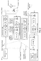
- FIG. 1 is a block diagram illustrating a full-duplex system, according to some implementations.
- Full-duplex system 100 may perform cancellation of self-interference signal 152 in the digital domain.
- self-interference signal 152 may contain both self-interference and other signal components, such as the wanted RX signal (e.g., a signal from another user equipment device, such as a base station).
- the wanted RX signal e.g., a signal from another user equipment device, such as a base station.
- self-interference signal 152 may refer to the self-interference, unless otherwise described.
- Full-duplex system 100 includes a transmission (TX) signal path, a receiving (RX) signal path, and a feedback signal path (e.g., feedback path).
- the TX signal path includes digital TX circuit 102 and analog TX circuit 104.
- the RX signal path includes analog RX circuit 112 and digital RX circuit 114. Although certain components are illustrated as belonging to analog TX circuit 104, feedback receiver circuit 106, analog RX circuit 112, or digital RX circuit 114, it may be noted that components of a particular circuit may be part of another circuit. For example, ADC 130 may be considered part of the analog RX circuit 112. In another example, DAC 120 may be considered part of digital TX circuit 102.
- the feedback signal path includes feedback receiver circuit 106. Feedback receiver circuit 106 may obtain a copy of analog TX signal 151 and convert the analog TX signal 151 into a digital representation, i.e., digital TX signal 153. Feedback receiver circuit 106 sends digital TX signal 153 to digital RX circuit 114. Digital RX circuit 114 uses digital TX signal 153 to cancel at least the transmission noise component of self-interference signal 152 in the digital domain.
- digital RX circuit 114 may include ADC 130, summation circuit 132, and digital RX signal processing circuit 134.
- Full-duplex system 100 may also include a circulator 108.
- the circulator 108 allows a signal to enter a first port and exit an adjacent second port.
- circulator 108 allows analog TX signal 151 to enter into port one (e.g., connection between analog TX circuit 104 and circulator 108) and exit port two (e.g., connection between circulator 108 and antenna 110) to transmit analog TX signal 151 using antenna 110.
- Circulator 108 may attenuate analog TX signal 151 traveling from port one to port three.
- self-interference signal 152 output at port three may be much weaker than analog TX signal 151 at port one or port two.
- other components for achieving isolation may be used, e.g. tunable or non-tunable duplex filters, or separate antenna structures, achieving some isolation between the signals.
- Antenna 110 may be a single antenna or multiple antennas. It may be noted that full-duplex system 100 illustrates various components for purposes of illustration, rather than limitation. I may be noted that the same, fewer, more, or different components may be implemented.
- full-duplex system 100 generates self-interference signal 152.
- the analog RX circuit 112 of full-duplex system 100 may also receive the analog TX signal 151 (i.e., self-interference signal 152).
- the analog TX signal 151 transmitted by full-duplex system 100 may be a significantly distorted version of digital TX baseband signal 150.
- Self-interference signal 152 may include three noise components: a linear noise component, a non-linear noise component, and a transmitter noise component.
- a linear noise component corresponds to the frequency of the transmitted baseband signal, e.g., at or near frequency of the digital TX baseband signal 150 after up conversion by up converter 122 to the carrier frequency.
- the linear noise component is a known signal because the frequency of the baseband signal (e.g., digital TX baseband signal 150) is known.
- the linear noise component may be attenuated and include reflections (e.g., echoes) from the environment or from within the full-duplex system 100 itself.
- the linear noise component may be a linear combination of the different delayed copies of the original transmitted baseband signal.
- the non-linear noise component may include harmonics of digital TX baseband signal 150.
- analog TX circuit 104 may receive digital TX baseband signal 150 and output non-linear squared, cubic, and higher order terms.
- the harmonics may have significant frequency content close to the transmitted baseband signal.
- Harmonics may be signal distortions that occur at equally spaced frequency intervals from the transmitted baseband frequency. Apart from harmonics, also so-called mixing products may be present. These mixing products appear when feeding at least two signal components with different frequencies to an element that has non-linear properties. It may be noted that since the transmitted baseband frequency is known, the non-linear noise components of self-interference signal 152 may also be known.
- a transmitter noise component also referred to as broadband noise
- Full-duplex system 100 e.g. RX signal path of full-duplex system 100
- the transmitter noise component may be an unwanted signal (e.g., noise) above the noise floor of the full-duplex radio.
- the transmitter noise component may be generated from high power components, such as power amplifier 124 or preceding components like up converter 122.
- the transmitter noise component is random and not known. Known noise signals may be inferred by an algorithm and canceled accordingly. Unknown noise signals are random, may not be inferred by an algorithm, and may be canceled by a copy of the unknown signal where the unknown signal is generated. It may be noted that a known noise signal may also be canceled by a copy of the known noise signal where the known noise signal is generated.
- circulator 108 may not perfectly isolate analog TX signal 151 from analog RX circuit 112 (e.g., port one to port 3).
- circulator 108 may couple an attenuated version of analog TX signal 151 (e.g., self-interference signal 152) to analog RX circuit 112.
- self-interference signal 152 may include echo copies of analog TX signal 151 received from the reflection of the analog TX signal 151 on objects in the environment subsequent transmission.
- the self-interference signal 152 is 110dB.
- the linear noise component of self-interference signal 152 may be 110dB, for example.
- the non-linear noise component of self-interference signal 152 may be 80dB, for example.
- the transmitter noise component of self-interference signal 152 may be 50dB, for example.
- Summation circuits may be implemented in various ways.
- summation circuit may be a coupler, such as a directional coupler.
- a coupler may split a signal into two copies with selectable power ratio.
- the splitting of a signal such as analog TX signal 151, may be used to tap a copy of the analog TX signal 151 after the power amplifier 124.
- the copy of analog TX signal 151 may be sent to feedback receiver circuit 106.
- a very small fraction of the signal e.g., attenuated analog TX signal 151
- the attenuated analog TX signal 151 may be sufficient to operate the feedback receiver 106.
- couplers may also be used to combine two signals into a single signal i.e. a summation operation or function.
- the summation operation of couplers may be used to implement the summation circuits, such as summation circuit 132.
- Couplers may also perform a subtraction operation. For example, a subtraction operation may be implemented by summing a signal after a 180-degree phase shift. It may be noted that other circuits may be used to implement the operations of summation circuits.
- a connection of two signals via two resistors may perform similar operations as described above with respect to summation circuits.
- summation circuit 232D or 232A or 232B of Figure 2 may be implemented with two resistors.
- summation circuits such as summation circuits 132, may be realized by digital adders.
- the addition (or subtraction) operations may be performed by a processor e.g. a digital signal processor (DSP) or by dedicated hardware.
- DSP digital signal processor
- digital TX circuit 102 sends digital TX baseband signal 150 to analog TX circuit 104. It may be noted that additional components may exist between digital TX circuit 102 and analog TX circuit 104.
- Analog TX circuit 104 converts digital TX baseband signal 150 into an analog signal (e.g., analog TX signal 151) using digital-to-analog converter (DAC) 120.
- Analog TX signal 151 is up-converted to a carrier frequency by up converter 122.
- digital-to-analog converter (DAC) 120 and up converter 122 may be combined into a single unit, e.g. a so-called RF-DAC that generates the analog RF signal directly from the digital TX baseband signal 150.
- Power amplifier 124 amplifies analog TX signal 151 to the appropriate power level for transmission.
- the output of power amplifier 124 is coupled to circulator 108.
- analog TX signal 151 is transmitted though port one of circulator 108 to a port two of circulator 108, where antenna 110 may transmit analog TX signal 151 as a wireless signal.
- the RX signal path of full-duplex system 100 may also receive at least an attenuated version of analog TX signal 151, illustrated as self-interference signal 152.
- Analog RX circuit 112 may receive self-interference signal 152 responsive to the transmission of analog TX signal 151.
- the low-noise amplifier (LNA) 126 of analog RX circuit 112 may receive self-interference signal 152.
- LNA 126 may send self-interference signal 152 to down converter 128 to convert self-interference signal 152 from a carrier frequency to an analog representation of self-interference signal 152 in baseband.
- Down converter sends self-interference signal 152 in baseband to ADC 130 of digital RX circuit 114.
- ADC 130 converts the self-interference signal 152 to a digital representation. Similar to the TX signal path, the functionalities of multiple components in the RX signal path may be merged into one or more components having the combined functionalities of the individual components.
- Summation circuit 132 receives digital TX signal 153, and the digital representation of self-interference signal 152. It may be noted that in some implementations, digital TX signal 153 may include the linear noise component, non-linear noise component, and transmitter noise component and be used to cancel all or some of the noise components from self-interference signal 152.
- summation circuit 132 of digital RX circuit 114 may cancel at least transmitter noise component of the digital representation of self-interference signal 152 using digital TX signal 153 (as will be described further below).
- digital TX signal 153 may be used to cancel noise components (e.g., linear noise component, non-linear noise component, or transmitter noise component) is self-interference signal 152 that are directly from leakage of circulator 108 (e.g., from port 1 to port 3), and may be used to cancel echoes of analog TX signal 151.
- the echoes of analog TX signal 151 may be part of self-interference signal 152, be external echoes that stem from reflections after circulator 108. These echoes may be delayed and phase shifted. Both the delay and phase shift of the echoes may be taken into account by digital RX circuit 114.
- the noise components of self-interference signal 152 may be canceled to the noise floor of full-duplex system 100.
- feedback receiver circuit 106 may tap analog TX circuit 104 at the output of power amplifier 124 to receive a copy of analog TX signal 151.
- Feedback receiver circuit 106 may convert the copy of analog TX signal 151 to a digital representation of analog TX signal 151 (e.g., digital TX signal 153).
- Digital TX signal 153 may be used by digital RX circuit 114 to digitally cancel (e.g., cancel in the digital domain) at least the transmission noise component of self-interference signal 152 associated with the transmission of analog TX signal 151 in full-duplex system 100.
- summation circuit 132 of digital RX circuit 114 may be coupled to the ADC 138 of feedback receiver circuit 106 to receive digital TX signal 153.
- Digital RX circuit 114 may use digital TX signal 153 to digitally cancel at least the transmitter noise component of self-interference signal 152.
- feedback receiver circuit 106 receives a copy of analog TX signal 151 and down converts the copy of analog TX signal 151 into baseband using down converter 136.
- Down converter 136 provides analog TX signal 151 in baseband to ADC 138.
- ADC 138 converts analog TX signal 151 into a digital representation (e.g., digital TX signal 153).
- Feedback receiver circuit 106 sends digital TX signal 153 to summation circuit 132 of digital RX circuit 114 where the digital TX signal 153 is used to cancel at least the transmitter noise component of self-interference signal 152.
- self-interference happens due to several phenomena occurring at different places within the TX and RX signal paths and outside of the full-duplex system 100, e.g. external echoes due to external reflections.
- the level of interference may vary by several orders of magnitude. For example, the further away a reflection occurs the weaker the self-interference.
- the different noise components of the transmitted signal e.g., analog TX signal 151, may also have different magnitudes. For weaker echoes, the dominant noise components contribute significantly to self-interference.
- Weaker echoes may be easily cancelled in the digital domain by taking the digital TX baseband signal 150 into account (e.g., disregarding non-linear noise component and transmitter noise) (e.g., illustrated by arrow connecting digital baseband signal 150 to summation circuit 132).
- the cancellation using the digital TX baseband signal 150 may be performed after all transmission / reception and associated analog and digital signal processing.
- the cancellation may not be constraint by any real-time requirements.
- the aforementioned cancellation may be referred to as outer cancelation or outer digital cancellation.
- the cancellation may be performed in the digital domain where it is comparatively easy to calculate multiple delayed and amplitude/phase adapted copies of a signal and in outer compensation, which is not time critical.
- RX/TX signal path e.g., RX/TX processing chain
- Cancellation that is immersed into the RX/TX signal path may be referred to as inner cancellation or inner digital cancellation.
- Inner cancellation may take advantage of intermediate signals, e.g., digital TX signal 153, or may be applied to the intermediate signals, as described further below.
- Non-in-band full-duplex systems may perform concurrent transmission and reception, although not necessarily on the same radio channel or frequency band.
- Non-in-band full-duplex systems may be susceptible to self-interference due to concurrent operation of transmission (TX) and reception (RX).
- TX transmission
- RX reception
- the self-interference of non-in-band full-duplex systems may be at least partly mitigated by filters e.g. duplex filters.
- duplex filters may contribute to the cost of the RF frontend.
- duplexer may be required for each band.
- increasing data rates by spatial multiplexing may require several TX or RX antennas and several duplexers for a single frequency band.
- duplexers may be replaced with circulators that can provide isolation in multiple frequency bands.
- Duplexers may also be replaced by tunable duplexers that can be tuned to different frequency bands. Tunable duplexers and circulators may not provide the isolation to operate the RX signal path with full sensitivity.
- a transmitter may be used instead of or in addition to analog TX circuit 104.
- a transmitter may be an electronic device that produces radio signals (e.g. analog TX signal 151) using an antenna, such as antenna 110.
- Some, all, or none of the components of analog TX circuit 104 may be implemented in a transmitter.
- the transmitter may include a power amplifier, such as power amplifier 124.
- TX circuit may refer to all or part of digital TX circuit 102 or analog TX circuit 104.
- RX circuit may refer to all or part of analog RX circuit 112 or digital RX circuit 114.
- Figure 2 is a block diagram illustrating a full-duplex system, according to other implementations. It may be noted that Figure 2 may have similar or corresponding features with respect to Figure 1 .
- Full-duplex system 200 includes delay phase amplifier 240, delay phase amplifier 241, one or more additional summation circuits 232, and compensating transmitter circuit 216.
- Compensating transmitter circuit 216 may include DAC 242, up converter 243, and amplifier 244 (e.g., tunable amplifier).
- amplifier 244 may be a tunable amplifier that may be able to provide tunable amplification to a received signal.
- amplifier 244 may be preceded or followed by a tunable attenuator to achieve amplification tuning.
- amplifier 244 may be an attenuator, e.g., an amplifier with an amplification ratio below 1 or below 0dB. This may be the case if the signal coming from a preceding stage is strong enough so that no amplification is used.
- the term amplifier is used in this more general meaning throughout the disclosure, unless described othewise.
- amplifier 244 may include or be combined with a phase shifter in order to set the phase of, for example, the analog TX baseband signal 254, to optimize cancellation.
- phase and amplitude tuning may not be implemented as phase and amplitude of the self-interference may be constant.
- full-duplex system 200 may cancel self-interference signal 152 and reduce the dynamic range requirement of ADC, such as ADC 138 or ADC 130.
- full-duplex system 200 may reduce the linearity requirement of components, such as LNA 126, mixer (not shown), or other components.
- Linearity requirement may refer to the ability of a circuit to amplify an input signal and generate an output signal without altering the content of the input signal.
- feedback receiver circuit 106 may be implemented to digitally cancel at least the transmitter noise component of self-interference signal 152 associated with the transmission of analog TX signal 151 in full-duplex system 200.
- Feedback receiver circuit 106 may be configured to receive a copy of analog TX signal 151 at the output of power amplifier 124 of analog TX circuit 104 and a feedback cancellation signal 255 from analog TX circuit 104 at some point prior to the power amplifier 124.
- feedback receiver circuit 106 may use feedback cancellation signal 255 from an amplifier, such as delay phase amplifier 240 or delay phase amplifier 241 or both, to cancel a portion of analog TX signal 151 prior to ADC 138.
- delay phase amplifier 241 taps analog TX circuit 104 after up converter 122 and prior to power amplifier 124.
- the aforementioned tap samples a "clean" analog TX signal 151 before the PA, a clean analog TX signal 151 may be a signal without the noise or distortions caused by power amplifier 124. Clean analog TX signal 151 may be used to cancel the dominant linear part of the analog TX signal 151 to better receive non-linear noise components of analog TX signal 151 and to reduce dynamic range of the ADC 138.
- delay phase amplifier 240 or delay phase amplifier 241 or both may be replaced by a tunable attenuator and phase shifter.
- another dedicated DAC may be used instead of picking up the signal after the DAC 120 and before up converter 122.
- the dedicated DAC may be fed with a copy of the digital TX baseband signal 150 including the desired phase and amplitude change.
- the desired phase and amplitude change maybe calculated in the digital domain, e.g. by multiplying with the desired amplitude modulation and by a complex multiplication with the desired phase rotation. A larger fraction of the cancellation may be performed in the digital domain taking advantage of Moore's law. Canceling a portion of analog TX signal 151 may reduce the signal strength of analog TX signal 151 and reduce the dynamic range requirement of ADC 138.
- the dynamic range requirement of ADC 138 may also be reduced by 30dB (e.g., equivalent to a 5-bit reduction of ADC 138). It may be noted that the reduced dynamic range of the ADC, or equivalently reducing the number of bits of a DAC, allows for a reduction in power consumption.
- Delay phase amplifier 240 or 241 may provide signal delay or amplitude or phase alignment of feedback cancellation signal 255.
- Feedback receiver circuit 106 may use feedback cancellation signal 255 to cancel a portion of the analog TX circuit 104 using summation circuit 232B or 232A, depending on the implementation.
- the remaining portion of analog TX signal 151 (the portion remaining after canceling analog TX signal 151 using feedback cancellation signal 255) may be sent to ADC 138 to generate a digital representation of the remaining portion of analog TX signal 151 (e.g., digital TX signal 253).
- Feedback receiver circuit 106 may send digital TX signal 253 to digital RX circuit 114.
- Digital RX circuit 114 may use digital TX signal 253 to digitally cancel at least transmitter noise component of self-interference signal 152. It may be noted that, in some implementations, power amplifier 124 may be responsible for a majority, if not all, transmitter noise component of self-interference signal 152.
- an amplifier such as delay phase amplifier 240 or 241 is coupled between analog TX circuit 104 and feedback receiver circuit 106 to tap analog TX circuit 104 and to provide feedback cancellation signal 255 to feedback receiver circuit 106.
- delay phase amplifier 241 taps analog TX circuit 104 after up converter 122 and prior to power amplifier 124.
- delay phase amplifier 240 taps analog TX circuit 104 after DAC 120 and before up converter 122.
- analog TX circuit 104 may be tapped by both delay phase amplifier 240 and delay phase amplifier 241 at the aforementioned locations.
- analog TX circuit 104 may have multiple successively coupled up converters, e.g. first create a signal at an intermediate frequency that is subsequently up converted to the final frequency.
- Analog TX circuit 104 may be tapped at the intermediate frequency.
- feedback receiver circuit 216 may similarly have multiple downconversion stages and may combine the tapped signal at a corresponding downconversion stage.
- intermediate frequencies are not explicitly mentioned, but it may be understood that all compensations may also be done at intermediate frequencies.
- digital RX circuit 114 may use digital TX signal 253 to digitally cancel at least the transmitter noise component and the non-linear noise component of self-interference signal 152.
- non-linear noise component may be added to digital TX signal 253.
- the digital TX signal 253 is not a direct copy of the leaked analog TX signal 151.
- the digital TX signal 253 may be self-interference signal 152 less the feedback cancellation signal 255.
- self-interference signal 152 e.g., including direct and echoes of the analog TX signal 151 that are reflected after the antenna
- both direct and echoes of analog TX signal 151 may be canceled with a suitable phase and amplitude adaptation.
- the feedback cancellation signal 255 may not be measured explicitly by feedback receiver 106, because it can be derived from digital TX baseband signal 150.
- feedback cancellation signal 254 and digital TX baseband signal 150 are identical, besides the amplification and some phase shift. Therefore both signals may be combined by digital RX circuit 114, taking the phase and amplitude into account e.g. by multiplication with an amplitude and phase factor (not shown) before the digital cancellation in summation circuit 132.
- Deviations from the ideal TX signal, in particular non-linear noise (e.g. non-linear distortions) and transmitter noise may be captured by feedback receiver 106.
- the transmitter noise component may not be possible to predict from the digital TX baseband signal 150.
- the non-linear noise component may also be measured implementation by feedback receiver 106 that may help to reduce computation complexity in the digital domain. For example, while these distortions, such as a non-linear noise component may be calculated in the digital domain, calculating in the digital domain may require additional processing power and increase the power consumption.
- compensating transmitter circuit 216 may be implemented to cancel at least part of the self-interference signal 152 (e.g., linear noise component) in the analog domain to reduce the dynamic range requirement of ADC 130 of digital TX circuit 102 or the linearity requirement of LNA 126 (or other components, such as a mixer in down converter 128).
- Digital TX circuit 102 may be coupled to compensating transmitter circuit 216 and provide digital TX baseband signal 150 to compensating transmitter circuit 216.
- Compensating transmitter circuit 216 may convert digital TX baseband signal 150 to an analog representation (e.g., analog TX baseband signal 254) using DAC 242. Phase and amplitude alignment can be performed by digital multiplication before DAC 242 or by tunable attenuator or amplifier and phase shifters.
- compensating transmitter circuit 216 may send analog TX baseband signal 254 to analog RX circuit 112 to cancel at least the linear noise component of self-interference signal 152 using analog TX baseband signal 254. It may be noted that in some implementations if a single tap is used after DAC 242 to summation circuit 232D, compensating transmitter circuit 216 may not include up converter 243 or amplifier 244, and analog TX baseband signal 254 may not be sent to summation circuit 232C. Analog TX baseband signal 254 may be received prior to ADC 130 of digital RX circuit 114 and after down converter 128 of analog RX circuit 112. In such an implementation, up converter 243 and amplifier 244 may be omitted from compensating transmitter circuit 216.
- compensating transmitter circuit 216 may process digital TX baseband signal 150 using DAC 242, followed by up conversion by up converter 243, and amplification by amplifier 244 (e.g., tunable amplifier) to output analog TX baseband signal 254.
- Compensating transmitter circuit 216 may send analog TX baseband signal 254 to summation circuit 232C of analog RX circuit 112.
- Compensating transmitter circuit 216 sends analog TX baseband signal 254 to a position before LNA 126 of analog RX circuit 112 to cancel at least the linear noise component of self-interference signal 152 and reduce the linearity requirement of LNA 126.
- compensating transmitter circuit 216 may provide analog TX baseband signal 254 to summation circuit 232D and to summation circuit 232C, as described above. It may be noted that in other implementations, analog TX baseband signal 254 may contain the linear noise component and the non-linear noise component of self-interference signal 152 and be used to cancel linear noise component and non-linear noise component of self-interference signal 152 in a similar manner as described above. The non-linear noise component of self-interference signal 152 may be calculated from digital TX baseband signal 150 via digital processing by simulating the known non-linearities of power amplifier 124. It may also be appreciated that in other implementations, digital TX circuit 102 may send a signal (represented by the dashed line from digital TX circuit 102 to digital RX circuit 114) to cancel the non-linear noise component of self-interference signal 152.
- FIG. 3 is a block diagram illustrating a full-duplex system, according to implementations.
- full-duplex system 300 includes tap delay 345 and summation circuit 332.
- Tap delay 345 may tap the output of analog TX circuit 104 to capture a copy of analog TX signal 151.
- Summation circuit 332 may combine analog TX signal 151 from tap delay 345 with analog TX baseband signal 254 from compensating transmitter circuit 216.
- Summation circuit 332 may send the combined signal to analog RX circuit 112 to cancel a portion of self-interference signal 152 via summation circuit 232C and reduce the dynamic range requirement of at least ADC 130, as well as components in compensating transmitter circuit 216 e.g. DAC 242.
- summation circuit 332 may be replaced by two individual summation circuits. Each one of the two individual summation circuits may be used to cancel the output of tap delay 345 or the output from compensating transmitter circuit 216.
- tap delay 345 may be a single tap delay. Tap delay 345 may make delay and/or phase adjustments to analog TX signal 151. Tap delay 345 may be used to cancel self-interference from the direct path between the port 1 and port 3 of circulator 108, rather than echoes of analog TX signal 151. Cancellation of the linear noise component, the non-linear noise component, and the transmitter noise component may performed in a similar manner as described with respect to the above Figures. In other implementations, more than one tap delay 345 may be implemented.
- FIG. 4 is a block diagram illustrating a full-duplex system, according to some implementations.
- full-duplex system 400 includes circulator 418 and digital predistortion (DPD) circuit 446.
- circulator 418 may be implemented with similar elements as circulator 108. Rather than an antenna, circulator 418 may have a reflector at port two at which an antenna would otherwise be connected.
- Circulator 418 may generate a similar delay or phase change of analog TX signal 151 as circulator 108 generates with self-interference signal 152.
- Circulator 418 may tap analog TX circuit 104 at the output of power amplifier 124 for a copy of analog TX signal 151.
- Circulator 418 may output, at port three, analog TX signal 151 with delay or phase change similar to self-interference signal 152.
- Summation circuit 332 may combine analog TX signal 151 from circulator 418 with analog TX baseband signal 254 from compensating transmitter circuit 216.
- the combined signal may be used to cancel a portion of self-interference signal 152 and reduce the dynamic range requirement of at least ADC 138 and ADC 130, as well as components in compensating transmitter circuit 216.
- a filter with a similar delay as circulator 108 or a filter with a tunable delay may be implemented.
- a duplexer can be used which may be implemented as Surface Acoustic Wave (SAW) filter or Bulk Acoustic Wave (BAW) filter or other technology.
- the filter delay may be similar to the delay caused by circulator or duplexer 108.
- circulator may refer to any implementation (e.g., filter, duplexer, etc.).
- identical or similar units for both circulator 108 and circulator 418 are used.
- Circulator418 may not provide insulation of TX and RX signals from one another and may be simpler, cheaper, and smaller. Cancellation of the linear noise component, the non-linear noise component, and the transmitter noise component may be performed in a similar manner as described with respect to the above Figures.
- digital TX circuit 102 may include DPD circuit 446. It may also be appreciated that DPD circuit 446 may also be implemented in one or more of the full-duplex systems described with respect to Figures 1-3 . DPD circuit 446 may provide digital predistortion for transmission linearization of analog TX signal 151. DPD circuit 446 may provide DPD in parallel with inner digital cancellation, while outer digital cancellation considers DPD and imperfections of DPD later during RX processing. All digital processing may be completed before the transmission of analog TX signal 151. In other implementations, DPD circuit may include multi-stage DPD (e.g., using multiple iterations). In multi-stage DPD, a subset of the stages may be considered for inner digital cancellation.
- a model of the imperfections of the DPD may be used.
- the imperfections of the DPD may be considered as noise on top of the ideal TX signal and eventually subtracted in the digital domain, either due to measurements by the feedback receiver circuit 106 or by further, more precise calculations available at a later time.
- the digital TX baseband signal 150 may not be considered fully “clean", as it contains predistortion components that are used so that the final TX signal is undistorted or less distorted.
- the predistortion components may be canceled and are not actually present in the analogue TX signal 151.
- the cancellation step actually introduces the predistortion components into the digital TX signal 253.
- the introduced predistortion components may be cancelled in subsequent digital processing stages.
- the predistortion components are known because they have been deliberately introduced by the DPD, they can be subtracted later on in the digital RX circuit 114.
- outer digital cancellation may receive a copy of the predistorted signal or information about the predistortion components.
- the digital TX baseband signal 150 may still be considered "clean" as regards to TX noise and other components that are not targeted by DPD and still function as described in the present disclosure.
- adaptation loops may be implemented. Adaptation loops may include channel adaptation, parameter adaptation, estimation, or correlation, for example. It may be noted that in some implementations of the full-duplex systems of Figures 1-4 , outer digital cancellation loops may take into account cancellation already performed by inner cancellation (e.g., inner analog cancellation, inner digital cancellation), including inner loop imperfections, (e.g., canceling residual interference from imperfections of the inner loops). The aforementioned is illustrated in Figure 4 by the order of the two dashed boxes labeled inner digital cancellation and outer digital cancellation.
- Outer digital cancellation may receive information about the performed inner digital cancellation and take into account that inner digital cancellation has already been performed by compensating transmitter circuit 216 and applied in analog RX circuit 112. Outer digital cancellation may omit cancelling of the components already cancelled by inner cancellation. In some examples including DPD, inner digital cancelation may not include the effect of DPD and achieve partial compensation. Outer digital cancellation may consider effects of DPD 446 and perform the outer digital cancellation later than inner digital cancellation, as described above. Outer digital cancellation loops may take additional information into account to reconstruct data as compared to the information available for inner digital cancellation loops. For example, the additional information includes information such as latest channel estimation such as samples received or processed after inner digital cancellation loops have been executed (e.g., even samples received after reception of the sample to be compensated).
- Channel prediction may be implemented for inner digital cancellation loops as the inner digital cancellation loops may be computed before the time of the actual transmission of a particular sample and therefore may rely on historic data. Additionally outer digital cancellation may also consider measurements from feedback receiver circuit 106 (i.e. digital TX signal 253) into account (not shown in Figure 4 ) on top of or instead of information from DPD 446. Inner digital cancellation may have compensated the linear components for several echoes, and outer digital cancellation may additionally cancel the effect of non-linear components and/or TX noise for these echoes. To save processing power, outer digital cancellation may consider the additional components for a selection of echoes, in particular for the strongest echoes, or select echoes depending on both strengths of the echoes and the required receive sensitivity, i.e. based on the expected performance degradation if not canceling a specific component of a specific echo.
- implementations described herein may be implemented in base stations, repeaters, and mobile devices, among others.
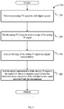
- Figure 5 is a flow diagram of operation of a full-duplex system, according to an implementation. It may be noted that features of Figures 1-4 may be described below to help illustrate method 500. Method 500 may be performed as operations. It may be noted that method 500 may be performed in any order and may include the same, more, or fewer operations. It may be noted that method 500 may be performed by one or more components of a full-duplex system described herein.
- Method 500 begins at operation 510 where full-duplex system 100 transmits analog TX signal 151 (e.g., sends analog TX signal 151 to circulator 108 for wireless transmission using antenna 110).
- feedback receiver circuit 106 taps analog TX circuit 104 at the output of power amplifier 124 to receive a copy of analog TX signal 151.
- feedback receiver circuit 106 converts analog TX signal 151 into a digital representation (e.g., digital TX signal 153).
- feedback receiver circuit 106 sends digital TX signal 153 to digital RX circuit 114 to digitally cancel at least the transmitter noise component of self-interference signal 152 associated with the transmission. Additional details of method 500 may be described at least with respect to Figure 1 .
- Figure 6 is a flow diagram of operation of a full-duplex system, according to an implementation. It may be noted that features of Figures 1-4 may be described below to help illustrate method 600. Method 600 may be performed as operations. It may be noted that method 600 may be performed in any order and may include the same, more, or fewer operations. It may be noted that method 600 may be performed by one or more components of full-duplex system described herein.
- Method 600 begins at operation 610 where feedback receiver circuit 106 of full-duplex system 200 taps analog TX circuit 104 to receive a feedback cancellation signal 255.
- full-duplex system 200 transmits analog TX signal 151.
- feedback receiver circuit 106 taps analog TX circuit 104 at the output of power amplifier 124 to receive a copy of analog TX signal 151.
- feedback receiver circuit 106 uses feedback cancellation signal 255 to cancel a portion of the analog TX signal 151 in the analog domain.
- compensating transmitter circuit 216 receives digital TX baseband signal 150 and converts digital TX baseband signal 150 into an analog representation (e.g. analog TX baseband signal 254).
- Compensating transmitter circuit 216 sends analog TX baseband signal 254 to the RX signal to cancel in the analog domain a linear noise component of the self-interference signal 152.
- feedback receiver circuit 106 provides a digital representation of the remaining portion of analog TX signal 151 (e.g., digital TX signal 253) to digital RX circuit 114 to digitally cancel at least the transmitter noise component of self-interference signal 152 associated with the transmission. Additional details of method 600 may be described at least with respect to Figure 2 and additionally Figures 3 and 4 .
- FIG 7 is a system diagram in which a full-duplex system may be implemented.
- user equipment (UE) device 700 may include a full-duplex system as described herein.
- the UE device 700 may include application circuitry 702, digital circuitry 704, Radio Frequency (RF) circuitry 706, front-end module (FEM) circuitry 708 and one or more antennas 710, coupled together at least as shown.
- RF Radio Frequency
- FEM front-end module
- digital TX circuit 102 and digital RX circuit 114 described with respect to Figures 1-4 may be included in digital circuitry 704.
- RF circuitry 706 may be included in RF circuitry 706 or FEM circuitry 708. It may be noted features described with respect to Figures 1-4 may be part of any of application circuitry 702, digital circuitry 704, Radio Frequency (RF) circuitry 706, or front-end module (FEM) circuitry 708. It may be noted that multiple instances of the mentioned circuitries may be present in the full duplex system. It may be noted that UE device 700 may also be a base station or access point or a repeater (also called a relay), possibly also containing a wired or wireless backhaul interface e.g. connected to application circuitry 702.
- RF Radio Frequency
- FEM front-end module
- TX and RX signals may contain the same user-data, but may be received from a terminal and forwarded (transmitted) towards a base station and vice versa.
- repeaters may operate on the same frequency for this forwarding of data, both from the base station to device (downlink) and vice versa (uplink) even though up- and downlink may operate on different frequencies or at different times, e.g., they may implement a hybrid of same-frequency full duplex and conventional duplex methods.
- the application circuitry 702 may include one or more application processors.
- the application circuitry 702 may include circuitry such as, but not limited to, one or more single-core or multi-core processors.
- the processor(s) may include any combination of general-purpose processors and dedicated processors (e.g., graphics processors, application processors, etc.).
- the processors may be coupled with and/or may include memory/storage and may be configured to execute instructions stored in the memory/storage to enable various applications and/or operating systems to run on the system.
- the digital circuitry 704 may include circuitry such as, but not limited to, one or more single-core or multi-core processors.
- the digital circuitry 704 may include one or more baseband processors and/or control logic to process baseband signals received from a receive signal path of the RF circuitry 706 and to generate baseband signals (e.g., digital TX baseband signal 150) for a transmit signal path of the RF circuitry 706.
- Digital circuity 704 may interface with the application circuitry 702 for generation and processing of the baseband signals and for controlling operations of the RF circuitry 706.
- the digital circuitry 704 may include a second generation (2G) baseband processor 704a, third generation (3G) baseband processor 704b, fourth generation (4G) baseband processor 704c, and/or other baseband processor(s) 704d for other existing generations, generations in development or to be developed in the future (e.g., fifth generation (5G), 6G, etc.).
- the digital circuitry 704 e.g., one or more of baseband processors 704a-d
- the radio control functions may include, but are not limited to, signal modulation/demodulation, encoding/decoding, radio frequency shifting, etc.
- modulation/demodulation circuitry of the digital circuitry 704 may include Fast-Fourier Transform (FFT), precoding, and/or constellation mapping/demapping functionality.
- FFT Fast-Fourier Transform
- encoding/decoding circuitry of the digital circuitry 704 may include convolution, tail-biting convolution, turbo, Viterbi, and/or Low Density Parity Check (LDPC) encoder/decoder functionality. Implementations of modulation/demodulation and encoder/decoder functionality are not limited to these examples and may include other suitable functionality in other implementations.
- the digital circuitry 704 may include elements of a protocol stack such as, for example, elements of an evolved universal terrestrial radio access network (EUTRAN) protocol (or successor protocols like 5 th Generation) (5G) including, for example, physical (PHY), media access control (MAC), radio link control (RLC), packet data convergence protocol (PDCP), and/or radio resource control (RRC) elements.
- EUTRAN evolved universal terrestrial radio access network
- 5G 5 th Generation
- a central processing unit (CPU) 704e of the digital circuitry 704 may be configured to run elements of the protocol stack for signaling of the PHY, MAC, RLC, PDCP, NAS and/or RRC layers.
- the digital circuitry may include one or more audio digital signal processor(s) (DSP) 704f.
- DSP audio digital signal processor
- the audio DSP(s) 704f may include elements for compression/decompression and echo cancellation and may include other suitable processing elements in other implementations.
- Components of the digital circuitry may be suitably combined in a single chip, a single chipset, or disposed on a same circuit board in some implementations.
- some or all of the constituent components of the baseband circuitry 704 and the application circuitry 702 may be implemented together such as, for example, on a system on a chip (SoC).
- SoC system on a chip
- the digital circuitry 704 may provide for communication compatible with one or more radio technologies.
- the digital circuitry 704 may support communication with an evolved universal terrestrial radio access network (EUTRAN) and/or other wireless metropolitan area networks (WMAN), a wireless local area network (WLAN), a wireless personal area network (WPAN).
- EUTRAN evolved universal terrestrial radio access network
- WMAN wireless metropolitan area networks
- WLAN wireless local area network
- WPAN wireless personal area network
- RF circuitry 706 may enable communication with wireless networks using modulated electromagnetic radiation through a non-solid medium.
- the RF circuitry 706 may include switches, filters, amplifiers, etc. to facilitate the communication with the wireless network.
- RF circuitry 706 may include a receive signal path which may include circuitry to down-convert RF signals received from the FEM circuitry 708 and provide baseband signals to the digital circuitry 704.
- RF circuitry 706 may also include a transmit signal path which may include circuitry to up-convert baseband signals provided by the digital circuitry 704 and provide RF output signals to the FEM circuitry 708 for transmission.
- the RF circuitry 706 may include a receive signal path and a transmit signal path.
- the receive signal path of the RF circuitry 706 may include mixer circuitry 706a, amplifier circuitry 706b and filter circuitry 706c.
- the transmit signal path of the RF circuitry 706 may include filter circuitry 706c and mixer circuitry 706a.
- RF circuitry 706 may also include synthesizer circuitry 706d for synthesizing a frequency for use by the mixer circuitry 706a of the receive signal path and the transmit signal path.
- the mixer circuitry 706a of the receive signal path may be configured to down-convert RF signals received from the FEM circuitry 708 based on the synthesized frequency provided by synthesizer circuitry 706d.
- the amplifier circuitry 706b may be configured to amplify the down-converted signals and the filter circuitry 706c may be a low-pass filter (LPF) or bandpass filter (BPF) configured to remove unwanted signals from the down-converted signals to generate output baseband signals.
- LPF low-pass filter
- BPF bandpass filter
- Output baseband signals may be provided to the digital circuitry 704 for further processing.
- the output baseband signals may be zero-frequency baseband signals, although this is not a requirement.
- mixer circuitry 706a of the receive signal path may comprise passive mixers, although the scope of the implementations is not limited in this respect.
- the mixer circuitry 706a of the transmit signal path may be configured to up-convert input baseband signals based on the synthesized frequency provided by the synthesizer circuitry 706d to generate RF output signals for the FEM circuitry 708.
- the baseband signals may be provided by the digital circuitry 704 and may be filtered by filter circuitry 706c.
- the filter circuitry 706c may include a low-pass filter (LPF), although the scope of the implementations is not limited in this respect.
- LPF low-pass filter
- the mixer circuitry 706a of the receive signal path and the mixer circuitry 706a of the transmit signal path may include two or more mixers and may be arranged for quadrature down conversion and/or up conversion respectively.
- the mixer circuitry 706a of the receive signal path and the mixer circuitry 706a of the transmit signal path may include two or more mixers and may be arranged for image rejection (e.g., Hartley image rejection).
- the mixer circuitry 706a of the receive signal path and the mixer circuitry 706a may be arranged for direct down conversion and/or direct up conversion, respectively.
- the mixer circuitry 706a of the receive signal path and the mixer circuitry 706a of the transmit signal path may be configured for super-heterodyne operation.
- the output baseband signals and the input baseband signals may be analog baseband signals, although the scope of the implementations is not limited in this respect.
- the output baseband signals and the input baseband signals may be digital baseband signals.
- the RF circuitry 706 may include analog-to-digital converter (ADC) and digital-to-analog converter (DAC) circuitry and the digital circuitry 704 may include a digital baseband interface to communicate with the RF circuitry 706.
- ADC analog-to-digital converter
- DAC digital-to-analog converter
- a separate radio IC circuitry may be provided for processing signals for each spectrum, although the scope of the implementations is not limited in this respect.
- the synthesizer circuitry 706d may be a fractional-N synthesizer or a fractional N/N+1 synthesizer, although the scope of the implementations is not limited in this respect as other types of frequency synthesizers may be suitable.
- synthesizer circuitry 706d may be a delta-sigma synthesizer, a frequency multiplier, or a synthesizer comprising a phase-locked loop with a frequency divider.
- the synthesizer circuitry 706d may be configured to synthesize an output frequency for use by the mixer circuitry 706a of the RF circuitry 706 based on a frequency input and a divider control input. In some implementations, the synthesizer circuitry 706d may be a fractional N/N+1 synthesizer.
- frequency input may be provided by a voltage controlled oscillator (VCO), although that is not a requirement.
- VCO voltage controlled oscillator
- Divider control input may be provided by either the digital circuitry 704 or the application circuitry 702 depending on the desired output frequency.
- a divider control input (e.g., N) may be determined from a look-up table based on a channel indicated by the applications processor 702.
- Synthesizer circuitry 706d of the RF circuitry 706 may include a divider, a delay-locked loop (DLL), a multiplexer and a phase accumulator.
- the divider may be a dual modulus divider (DMD) and the phase accumulator may be a digital phase accumulator (DPA).
- the DMD may be configured to divide the input signal by either N or N+1 (e.g., based on a carry out) to provide a fractional division ratio.
- the DLL may include a set of cascaded, tunable, delay elements, a phase detector, a charge pump and a D-type flip-flop.
- the delay elements may be configured to break a VCO period up into N d equal packets of phase, where N d is the number of delay elements in the delay line.
- N d is the number of delay elements in the delay line.
- synthesizer circuitry 706d may be configured to generate a carrier frequency as the output frequency, while in other implementations, the output frequency may be a multiple of the carrier frequency (e.g., twice the carrier frequency, four times the carrier frequency) and used in conjunction with quadrature generator and divider circuitry to generate multiple signals at the carrier frequency with multiple different phases with respect to each other.
- the output frequency may be a LO frequency (f LO ).
- the RF circuitry 706 may include an IQ/polar converter.
- FEM circuitry 708 may include a receive signal path which may include circuitry configured to operate on RF signals received from one or more antennas 710, amplify the received signals and provide the amplified versions of the received signals to the RF circuitry 706 for further processing.
- FEM circuitry 708 may also include a transmit signal path which may include circuitry configured to amplify signals for transmission provided by the RF circuitry 706 for transmission by one or more of the one or more antennas 710.
- the FEM circuitry 708 may include a TX/RX switch to switch between transmit mode and receive mode operation.
- the FEM circuitry may include a receive signal path and a transmit signal path.
- the receive signal path of the FEM circuitry may include a low-noise amplifier (LNA) to amplify received RF signals and provide the amplified received RF signals as an output (e.g., to the RF circuitry 706).
- the transmit signal path of the FEM circuitry 708 may include a power amplifier (PA) to amplify input RF signals (e.g., provided by RF circuitry 706), and one or more filters to generate RF signals for subsequent transmission (e.g., by one or more of the one or more antennas 710).
- PA power amplifier
- the UE device 700 may include additional elements such as, for example, memory/storage, display, camera, sensor, and/or input/output (I/O) interface.
- additional elements such as, for example, memory/storage, display, camera, sensor, and/or input/output (I/O) interface.
- one or more processing devices for performing the operations of the above described implementations are disclosed. Additionally, in implementations of the disclosure, a non-transitory computer readable storage medium stores instructions for performing the operations of the described implementations. Also in other implementations, systems for performing the operations of the described implementations are also disclosed
- the present disclosure also relates to an apparatus for performing the operations herein.
- This apparatus may be specially constructed for the required purposes, or it may include a general purpose computer selectively activated or reconfigured by a computer program stored in the computer.
- a computer program may be stored in a computer readable storage medium, such as, but not limited to, any type of disk including a floppy disk, an optical disk, a compact disc read-only memory (CD-ROM), a magnetic-optical disk, a read-only memory (ROM), a random access memory (RAM), an erasable programmable read-only memory (EPROM), an electrically erasable programmable read-only memory (EEPROM), a magnetic or optical card, or any type of media suitable for storing electronic instructions.
- a computer readable storage medium such as, but not limited to, any type of disk including a floppy disk, an optical disk, a compact disc read-only memory (CD-ROM), a magnetic-optical disk, a read-only memory (ROM), a random
- example or “exemplary” are used herein to mean serving as an example, instance, or illustration. Any aspect or design described herein as “example' or “exemplary” is not necessarily to be construed as preferred or advantageous over other aspects or designs. Rather, use of the words “example” or “exemplary” is intended to present concepts in a concrete fashion.
- the term “or” is intended to mean an inclusive “or” rather than an exclusive “or.” That is, unless specified otherwise, or clear from context, "X includes A or B" is intended to mean any of the natural inclusive permutations.
Landscapes
- Engineering & Computer Science (AREA)
- Signal Processing (AREA)
- Computer Networks & Wireless Communication (AREA)
- Transceivers (AREA)
- Noise Elimination (AREA)
Applications Claiming Priority (1)
| Application Number | Priority Date | Filing Date | Title |
|---|---|---|---|
| US15/197,528 US11451363B2 (en) | 2016-06-29 | 2016-06-29 | Digital-centric full-duplex architecture |
Publications (3)
| Publication Number | Publication Date |
|---|---|
| EP3285404A2 true EP3285404A2 (de) | 2018-02-21 |
| EP3285404A3 EP3285404A3 (de) | 2018-06-20 |
| EP3285404B1 EP3285404B1 (de) | 2020-04-29 |
Family
ID=59053895
Family Applications (1)
| Application Number | Title | Priority Date | Filing Date |
|---|---|---|---|
| EP17173593.9A Active EP3285404B1 (de) | 2016-06-29 | 2017-05-30 | Digital-zentrische vollduplex-architektur |
Country Status (2)
| Country | Link |
|---|---|
| US (1) | US11451363B2 (de) |
| EP (1) | EP3285404B1 (de) |
Families Citing this family (24)
| Publication number | Priority date | Publication date | Assignee | Title |
|---|---|---|---|---|
| US10110306B2 (en) | 2015-12-13 | 2018-10-23 | GenXComm, Inc. | Interference cancellation methods and apparatus |
| US10257746B2 (en) * | 2016-07-16 | 2019-04-09 | GenXComm, Inc. | Interference cancellation methods and apparatus |
| WO2018218089A1 (en) * | 2017-05-24 | 2018-11-29 | The Board Of Trustees Of The University Of Illinois | Self-interference cancellation for in-band full duplex single antenna communication systems |
| CN108768431A (zh) * | 2018-04-21 | 2018-11-06 | 成都定为电子技术有限公司 | 一种同时同频全双工对讲机及其实现方法 |
| US11150409B2 (en) | 2018-12-27 | 2021-10-19 | GenXComm, Inc. | Saw assisted facet etch dicing |
| US10673661B1 (en) * | 2019-03-28 | 2020-06-02 | Intel Corporation | Signal component cancellation for feedback receiver |
| US11431367B2 (en) * | 2019-06-28 | 2022-08-30 | Indian Institute Of Technology, Bombay | System for cancelling interference in a full-duplex wireline communication link |
| US10727945B1 (en) | 2019-07-15 | 2020-07-28 | GenXComm, Inc. | Efficiently combining multiple taps of an optical filter |
| US11152966B1 (en) * | 2019-09-10 | 2021-10-19 | Amazon Technologies, Inc. | Digital active interference cancellation for full duplex transmit-receive (TX-RX) concurrency |
| US11215755B2 (en) | 2019-09-19 | 2022-01-04 | GenXComm, Inc. | Low loss, polarization-independent, large bandwidth mode converter for edge coupling |
| US11539394B2 (en) | 2019-10-29 | 2022-12-27 | GenXComm, Inc. | Self-interference mitigation in in-band full-duplex communication systems |
| US11796737B2 (en) | 2020-08-10 | 2023-10-24 | GenXComm, Inc. | Co-manufacturing of silicon-on-insulator waveguides and silicon nitride waveguides for hybrid photonic integrated circuits |
| US11245430B1 (en) | 2020-08-14 | 2022-02-08 | Apple Inc. | Wireless transmitters having self-interference cancellation circuitry |
| US12001065B1 (en) | 2020-11-12 | 2024-06-04 | ORCA Computing Limited | Photonics package with tunable liquid crystal lens |
| US12057873B2 (en) | 2021-02-18 | 2024-08-06 | GenXComm, Inc. | Maximizing efficiency of communication systems with self-interference cancellation subsystems |
| EP4331120A1 (de) | 2021-04-29 | 2024-03-06 | Genxcomm, Inc. | Selbstinterferenzunterdrückungssubsysteme für mesh-netzwerkknoten |
| US11838056B2 (en) | 2021-10-25 | 2023-12-05 | GenXComm, Inc. | Hybrid photonic integrated circuits for ultra-low phase noise signal generators |
| US12206441B2 (en) | 2022-03-31 | 2025-01-21 | Dell Products L.P. | Detection and cancellation of unwanted signals in a wireless communication radio unit |
| US12224782B2 (en) | 2022-04-14 | 2025-02-11 | Dell Products L.P. | Detection, cancellation, and evaluation of signals in a wireless communication radio unit |
| US12003280B2 (en) | 2022-04-22 | 2024-06-04 | Dell Products L.P. | Analog domain loopback modes |
| CN115065374A (zh) * | 2022-04-27 | 2022-09-16 | 深圳市国电科技通信有限公司 | 电力线载波通信收发机和电力线载波通信系统 |
| TWI892088B (zh) * | 2023-02-21 | 2025-08-01 | 瑞昱半導體股份有限公司 | 收發器以及用來在收發器中抑制諧波訊號的方法 |
| US20250293719A1 (en) * | 2024-03-15 | 2025-09-18 | Analog Devices International Unlimited Company | Apparatus and methods for self-jamming cancellation in full duplex radios |
| CN118100981B (zh) * | 2024-04-19 | 2024-07-16 | 南京仁芯科技有限公司 | 全双工高速有线通信的回声消除方法、收发器系统及芯片 |
Family Cites Families (9)
| Publication number | Priority date | Publication date | Assignee | Title |
|---|---|---|---|---|
| GB8705155D0 (en) | 1987-03-05 | 1987-04-08 | Lucas Ind Plc | Fuel injection nozzles |
| EP2095516A2 (de) | 2006-11-06 | 2009-09-02 | Nokia Corporation | Analogsignalwegmodellierung für selbstinterferenzunterdrückung |
| US8306480B2 (en) | 2008-01-22 | 2012-11-06 | Texas Instruments Incorporated | System and method for transmission interference cancellation in full duplex transceiver |
| US20130259099A1 (en) | 2012-03-30 | 2013-10-03 | Qualcomm Incorporated | Tunable notch filter using feedback through an existing feedback receiver |
| EP3229375B1 (de) | 2013-07-01 | 2020-11-18 | Telefonaktiebolaget LM Ericsson (publ) | Digitale unterdrückung von senderzwischenmodulation bei einem empfänger |
| CN104518808B (zh) * | 2013-09-29 | 2017-07-14 | 华为技术有限公司 | 自干扰信号消除设备及方法 |
| WO2015171177A1 (en) | 2014-05-05 | 2015-11-12 | The Regents Of The University Of California | Full-duplex self-interference cancellation systems |
| US9847865B2 (en) | 2014-08-20 | 2017-12-19 | Huawei Technologies Co., Ltd. | System and method for digital cancellation of self-interference in full-duplex communications |
| WO2016073925A1 (en) * | 2014-11-06 | 2016-05-12 | GM Global Technology Operations LLC | Software programmable cellular radio architecture for wide bandwidth radio systems including telematics and infotainment systems |
-
2016
- 2016-06-29 US US15/197,528 patent/US11451363B2/en active Active
-
2017
- 2017-05-30 EP EP17173593.9A patent/EP3285404B1/de active Active
Non-Patent Citations (1)
| Title |
|---|
| None |
Also Published As
| Publication number | Publication date |
|---|---|
| US20180006795A1 (en) | 2018-01-04 |
| EP3285404A3 (de) | 2018-06-20 |
| US11451363B2 (en) | 2022-09-20 |
| EP3285404B1 (de) | 2020-04-29 |
Similar Documents
| Publication | Publication Date | Title |
|---|---|---|
| EP3285404B1 (de) | Digital-zentrische vollduplex-architektur | |
| US9647705B2 (en) | Digital self-interference residual cancellation | |
| US10284356B2 (en) | Self-interference cancellation | |
| CN108028673B (zh) | 收发机和用于减少收发机的自干扰的方法 | |
| TWI499224B (zh) | 多模式射頻存取技術裝置中可消除干擾之接收器及其方法 | |
| CN106464617B (zh) | 一种干扰消除的装置和方法 | |
| EP3210307B1 (de) | Vollduplex-funkgerät mit tx-leck-unterdrückung | |
| CN104518808B (zh) | 自干扰信号消除设备及方法 | |
| JP2013532447A (ja) | Rf消去基準を使用した中継器のためのハイブリッド無線アーキテクチャ | |
| CN104796170A (zh) | 生成补偿信号的方法和收发机设备 | |
| US20210050878A1 (en) | Integrated circuit for self-interference cancellation and method of performing full-duplex radio communication | |
| Kanumalli et al. | Mixed-signal based enhanced widely linear cancellation of modulated spur interference in LTE-CA transceivers | |
| EP3335391B1 (de) | Homodyn-empfängerkalibrierung | |
| US10623045B2 (en) | Receiver and a method for reducing a distortion component within a baseband receive signal | |
| JP2012060433A (ja) | 送受信機及びそれを用いた携帯電話用端末向けrfic並びに携帯電話用基地局 | |
| HK1191760B (en) | Interference cancellation in multi-mode radio access technology devices |
Legal Events
| Date | Code | Title | Description |
|---|---|---|---|
| PUAI | Public reference made under article 153(3) epc to a published international application that has entered the european phase |
Free format text: ORIGINAL CODE: 0009012 |
|
| STAA | Information on the status of an ep patent application or granted ep patent |
Free format text: STATUS: REQUEST FOR EXAMINATION WAS MADE |
|
| 17P | Request for examination filed |
Effective date: 20170530 |
|
| AK | Designated contracting states |
Kind code of ref document: A2 Designated state(s): AL AT BE BG CH CY CZ DE DK EE ES FI FR GB GR HR HU IE IS IT LI LT LU LV MC MK MT NL NO PL PT RO RS SE SI SK SM TR |
|
| AX | Request for extension of the european patent |
Extension state: BA ME |
|
| PUAL | Search report despatched |
Free format text: ORIGINAL CODE: 0009013 |
|
| AK | Designated contracting states |
Kind code of ref document: A3 Designated state(s): AL AT BE BG CH CY CZ DE DK EE ES FI FR GB GR HR HU IE IS IT LI LT LU LV MC MK MT NL NO PL PT RO RS SE SI SK SM TR |
|
| AX | Request for extension of the european patent |
Extension state: BA ME |
|
| RIC1 | Information provided on ipc code assigned before grant |
Ipc: H04B 1/525 20150101ALI20180511BHEP Ipc: H04B 1/12 20060101AFI20180511BHEP |
|
| GRAP | Despatch of communication of intention to grant a patent |
Free format text: ORIGINAL CODE: EPIDOSNIGR1 |
|
| STAA | Information on the status of an ep patent application or granted ep patent |
Free format text: STATUS: GRANT OF PATENT IS INTENDED |
|
| INTG | Intention to grant announced |
Effective date: 20190624 |
|
| GRAJ | Information related to disapproval of communication of intention to grant by the applicant or resumption of examination proceedings by the epo deleted |
Free format text: ORIGINAL CODE: EPIDOSDIGR1 |
|
| STAA | Information on the status of an ep patent application or granted ep patent |
Free format text: STATUS: REQUEST FOR EXAMINATION WAS MADE |
|
| GRAP | Despatch of communication of intention to grant a patent |
Free format text: ORIGINAL CODE: EPIDOSNIGR1 |
|
| STAA | Information on the status of an ep patent application or granted ep patent |
Free format text: STATUS: GRANT OF PATENT IS INTENDED |
|
| INTC | Intention to grant announced (deleted) | ||
| INTG | Intention to grant announced |
Effective date: 20191112 |
|
| GRAS | Grant fee paid |
Free format text: ORIGINAL CODE: EPIDOSNIGR3 |
|
| GRAA | (expected) grant |
Free format text: ORIGINAL CODE: 0009210 |
|
| STAA | Information on the status of an ep patent application or granted ep patent |
Free format text: STATUS: THE PATENT HAS BEEN GRANTED |
|
| AK | Designated contracting states |
Kind code of ref document: B1 Designated state(s): AL AT BE BG CH CY CZ DE DK EE ES FI FR GB GR HR HU IE IS IT LI LT LU LV MC MK MT NL NO PL PT RO RS SE SI SK SM TR |
|
| REG | Reference to a national code |
Ref country code: GB Ref legal event code: FG4D |
|
| REG | Reference to a national code |
Ref country code: CH Ref legal event code: EP |
|
| REG | Reference to a national code |
Ref country code: DE Ref legal event code: R096 Ref document number: 602017015506 Country of ref document: DE |
|
| REG | Reference to a national code |
Ref country code: AT Ref legal event code: REF Ref document number: 1264863 Country of ref document: AT Kind code of ref document: T Effective date: 20200515 |
|
| REG | Reference to a national code |
Ref country code: IE Ref legal event code: FG4D |
|
| REG | Reference to a national code |
Ref country code: DE Ref legal event code: R082 Ref document number: 602017015506 Country of ref document: DE Representative=s name: BARDEHLE PAGENBERG PARTNERSCHAFT MBB PATENTANW, DE Ref country code: DE Ref legal event code: R081 Ref document number: 602017015506 Country of ref document: DE Owner name: APPLE INC., CUPERTINO, US Free format text: FORMER OWNER: INTEL IP CORPORATION, SANTA CLARA, CALIF., US Ref country code: DE Ref legal event code: R081 Ref document number: 602017015506 Country of ref document: DE Owner name: APPLE INC., CUPERTINO, US Free format text: FORMER OWNER: INTEL IP CORPORATION, SANTA CLARA, CA, US |
|
| REG | Reference to a national code |
Ref country code: NL Ref legal event code: MP Effective date: 20200429 |
|
| REG | Reference to a national code |
Ref country code: LT Ref legal event code: MG4D |
|
| PG25 | Lapsed in a contracting state [announced via postgrant information from national office to epo] |
Ref country code: IS Free format text: LAPSE BECAUSE OF FAILURE TO SUBMIT A TRANSLATION OF THE DESCRIPTION OR TO PAY THE FEE WITHIN THE PRESCRIBED TIME-LIMIT Effective date: 20200829 Ref country code: PT Free format text: LAPSE BECAUSE OF FAILURE TO SUBMIT A TRANSLATION OF THE DESCRIPTION OR TO PAY THE FEE WITHIN THE PRESCRIBED TIME-LIMIT Effective date: 20200831 Ref country code: GR Free format text: LAPSE BECAUSE OF FAILURE TO SUBMIT A TRANSLATION OF THE DESCRIPTION OR TO PAY THE FEE WITHIN THE PRESCRIBED TIME-LIMIT Effective date: 20200730 Ref country code: LT Free format text: LAPSE BECAUSE OF FAILURE TO SUBMIT A TRANSLATION OF THE DESCRIPTION OR TO PAY THE FEE WITHIN THE PRESCRIBED TIME-LIMIT Effective date: 20200429 Ref country code: FI Free format text: LAPSE BECAUSE OF FAILURE TO SUBMIT A TRANSLATION OF THE DESCRIPTION OR TO PAY THE FEE WITHIN THE PRESCRIBED TIME-LIMIT Effective date: 20200429 Ref country code: NO Free format text: LAPSE BECAUSE OF FAILURE TO SUBMIT A TRANSLATION OF THE DESCRIPTION OR TO PAY THE FEE WITHIN THE PRESCRIBED TIME-LIMIT Effective date: 20200729 Ref country code: SE Free format text: LAPSE BECAUSE OF FAILURE TO SUBMIT A TRANSLATION OF THE DESCRIPTION OR TO PAY THE FEE WITHIN THE PRESCRIBED TIME-LIMIT Effective date: 20200429 |
|
| REG | Reference to a national code |
Ref country code: AT Ref legal event code: MK05 Ref document number: 1264863 Country of ref document: AT Kind code of ref document: T Effective date: 20200429 |
|
| PG25 | Lapsed in a contracting state [announced via postgrant information from national office to epo] |
Ref country code: BG Free format text: LAPSE BECAUSE OF FAILURE TO SUBMIT A TRANSLATION OF THE DESCRIPTION OR TO PAY THE FEE WITHIN THE PRESCRIBED TIME-LIMIT Effective date: 20200729 Ref country code: LV Free format text: LAPSE BECAUSE OF FAILURE TO SUBMIT A TRANSLATION OF THE DESCRIPTION OR TO PAY THE FEE WITHIN THE PRESCRIBED TIME-LIMIT Effective date: 20200429 Ref country code: HR Free format text: LAPSE BECAUSE OF FAILURE TO SUBMIT A TRANSLATION OF THE DESCRIPTION OR TO PAY THE FEE WITHIN THE PRESCRIBED TIME-LIMIT Effective date: 20200429 Ref country code: RS Free format text: LAPSE BECAUSE OF FAILURE TO SUBMIT A TRANSLATION OF THE DESCRIPTION OR TO PAY THE FEE WITHIN THE PRESCRIBED TIME-LIMIT Effective date: 20200429 |
|
| PG25 | Lapsed in a contracting state [announced via postgrant information from national office to epo] |
Ref country code: AL Free format text: LAPSE BECAUSE OF FAILURE TO SUBMIT A TRANSLATION OF THE DESCRIPTION OR TO PAY THE FEE WITHIN THE PRESCRIBED TIME-LIMIT Effective date: 20200429 Ref country code: NL Free format text: LAPSE BECAUSE OF FAILURE TO SUBMIT A TRANSLATION OF THE DESCRIPTION OR TO PAY THE FEE WITHIN THE PRESCRIBED TIME-LIMIT Effective date: 20200429 |
|
| PG25 | Lapsed in a contracting state [announced via postgrant information from national office to epo] |
Ref country code: DK Free format text: LAPSE BECAUSE OF FAILURE TO SUBMIT A TRANSLATION OF THE DESCRIPTION OR TO PAY THE FEE WITHIN THE PRESCRIBED TIME-LIMIT Effective date: 20200429 Ref country code: SM Free format text: LAPSE BECAUSE OF FAILURE TO SUBMIT A TRANSLATION OF THE DESCRIPTION OR TO PAY THE FEE WITHIN THE PRESCRIBED TIME-LIMIT Effective date: 20200429 Ref country code: EE Free format text: LAPSE BECAUSE OF FAILURE TO SUBMIT A TRANSLATION OF THE DESCRIPTION OR TO PAY THE FEE WITHIN THE PRESCRIBED TIME-LIMIT Effective date: 20200429 Ref country code: AT Free format text: LAPSE BECAUSE OF FAILURE TO SUBMIT A TRANSLATION OF THE DESCRIPTION OR TO PAY THE FEE WITHIN THE PRESCRIBED TIME-LIMIT Effective date: 20200429 Ref country code: ES Free format text: LAPSE BECAUSE OF FAILURE TO SUBMIT A TRANSLATION OF THE DESCRIPTION OR TO PAY THE FEE WITHIN THE PRESCRIBED TIME-LIMIT Effective date: 20200429 Ref country code: CZ Free format text: LAPSE BECAUSE OF FAILURE TO SUBMIT A TRANSLATION OF THE DESCRIPTION OR TO PAY THE FEE WITHIN THE PRESCRIBED TIME-LIMIT Effective date: 20200429 Ref country code: IT Free format text: LAPSE BECAUSE OF FAILURE TO SUBMIT A TRANSLATION OF THE DESCRIPTION OR TO PAY THE FEE WITHIN THE PRESCRIBED TIME-LIMIT Effective date: 20200429 Ref country code: RO Free format text: LAPSE BECAUSE OF FAILURE TO SUBMIT A TRANSLATION OF THE DESCRIPTION OR TO PAY THE FEE WITHIN THE PRESCRIBED TIME-LIMIT Effective date: 20200429 Ref country code: CH Free format text: LAPSE BECAUSE OF NON-PAYMENT OF DUE FEES Effective date: 20200531 Ref country code: LI Free format text: LAPSE BECAUSE OF NON-PAYMENT OF DUE FEES Effective date: 20200531 Ref country code: MC Free format text: LAPSE BECAUSE OF FAILURE TO SUBMIT A TRANSLATION OF THE DESCRIPTION OR TO PAY THE FEE WITHIN THE PRESCRIBED TIME-LIMIT Effective date: 20200429 |
|
| REG | Reference to a national code |
Ref country code: DE Ref legal event code: R097 Ref document number: 602017015506 Country of ref document: DE |
|
| PG25 | Lapsed in a contracting state [announced via postgrant information from national office to epo] |
Ref country code: SK Free format text: LAPSE BECAUSE OF FAILURE TO SUBMIT A TRANSLATION OF THE DESCRIPTION OR TO PAY THE FEE WITHIN THE PRESCRIBED TIME-LIMIT Effective date: 20200429 Ref country code: PL Free format text: LAPSE BECAUSE OF FAILURE TO SUBMIT A TRANSLATION OF THE DESCRIPTION OR TO PAY THE FEE WITHIN THE PRESCRIBED TIME-LIMIT Effective date: 20200429 |
|
| PLBE | No opposition filed within time limit |
Free format text: ORIGINAL CODE: 0009261 |
|
| STAA | Information on the status of an ep patent application or granted ep patent |
Free format text: STATUS: NO OPPOSITION FILED WITHIN TIME LIMIT |
|
| REG | Reference to a national code |
Ref country code: BE Ref legal event code: MM Effective date: 20200531 |
|
| PG25 | Lapsed in a contracting state [announced via postgrant information from national office to epo] |
Ref country code: LU Free format text: LAPSE BECAUSE OF NON-PAYMENT OF DUE FEES Effective date: 20200530 |
|
| 26N | No opposition filed |
Effective date: 20210201 |
|
| PG25 | Lapsed in a contracting state [announced via postgrant information from national office to epo] |
Ref country code: IE Free format text: LAPSE BECAUSE OF NON-PAYMENT OF DUE FEES Effective date: 20200530 Ref country code: FR Free format text: LAPSE BECAUSE OF NON-PAYMENT OF DUE FEES Effective date: 20200629 |
|
| PG25 | Lapsed in a contracting state [announced via postgrant information from national office to epo] |
Ref country code: SI Free format text: LAPSE BECAUSE OF FAILURE TO SUBMIT A TRANSLATION OF THE DESCRIPTION OR TO PAY THE FEE WITHIN THE PRESCRIBED TIME-LIMIT Effective date: 20200429 Ref country code: BE Free format text: LAPSE BECAUSE OF NON-PAYMENT OF DUE FEES Effective date: 20200531 |
|
| PG25 | Lapsed in a contracting state [announced via postgrant information from national office to epo] |
Ref country code: TR Free format text: LAPSE BECAUSE OF FAILURE TO SUBMIT A TRANSLATION OF THE DESCRIPTION OR TO PAY THE FEE WITHIN THE PRESCRIBED TIME-LIMIT Effective date: 20200429 Ref country code: MT Free format text: LAPSE BECAUSE OF FAILURE TO SUBMIT A TRANSLATION OF THE DESCRIPTION OR TO PAY THE FEE WITHIN THE PRESCRIBED TIME-LIMIT Effective date: 20200429 Ref country code: CY Free format text: LAPSE BECAUSE OF FAILURE TO SUBMIT A TRANSLATION OF THE DESCRIPTION OR TO PAY THE FEE WITHIN THE PRESCRIBED TIME-LIMIT Effective date: 20200429 |
|
| PG25 | Lapsed in a contracting state [announced via postgrant information from national office to epo] |
Ref country code: MK Free format text: LAPSE BECAUSE OF FAILURE TO SUBMIT A TRANSLATION OF THE DESCRIPTION OR TO PAY THE FEE WITHIN THE PRESCRIBED TIME-LIMIT Effective date: 20200429 |
|
| P01 | Opt-out of the competence of the unified patent court (upc) registered |
Effective date: 20230523 |
|
| REG | Reference to a national code |
Ref country code: GB Ref legal event code: 732E Free format text: REGISTERED BETWEEN 20240704 AND 20240710 |
|
| PGFP | Annual fee paid to national office [announced via postgrant information from national office to epo] |
Ref country code: DE Payment date: 20250402 Year of fee payment: 9 |
|
| PGFP | Annual fee paid to national office [announced via postgrant information from national office to epo] |
Ref country code: GB Payment date: 20260313 Year of fee payment: 10 |