EP3286593B1 - Integrationskegel für eine beleuchtungsvorrichtung - Google Patents
Integrationskegel für eine beleuchtungsvorrichtung Download PDFInfo
- Publication number
- EP3286593B1 EP3286593B1 EP16722452.6A EP16722452A EP3286593B1 EP 3286593 B1 EP3286593 B1 EP 3286593B1 EP 16722452 A EP16722452 A EP 16722452A EP 3286593 B1 EP3286593 B1 EP 3286593B1
- Authority
- EP
- European Patent Office
- Prior art keywords
- light
- solid state
- state lighting
- cone
- lighting device
- Prior art date
- Legal status (The legal status is an assumption and is not a legal conclusion. Google has not performed a legal analysis and makes no representation as to the accuracy of the status listed.)
- Active
Links
Images




Classifications
-
- F—MECHANICAL ENGINEERING; LIGHTING; HEATING; WEAPONS; BLASTING
- F21—LIGHTING
- F21V—FUNCTIONAL FEATURES OR DETAILS OF LIGHTING DEVICES OR SYSTEMS THEREOF; STRUCTURAL COMBINATIONS OF LIGHTING DEVICES WITH OTHER ARTICLES, NOT OTHERWISE PROVIDED FOR
- F21V9/00—Elements for modifying spectral properties, polarisation or intensity of the light emitted, e.g. filters
- F21V9/30—Elements containing photoluminescent material distinct from or spaced from the light source
-
- F—MECHANICAL ENGINEERING; LIGHTING; HEATING; WEAPONS; BLASTING
- F21—LIGHTING
- F21V—FUNCTIONAL FEATURES OR DETAILS OF LIGHTING DEVICES OR SYSTEMS THEREOF; STRUCTURAL COMBINATIONS OF LIGHTING DEVICES WITH OTHER ARTICLES, NOT OTHERWISE PROVIDED FOR
- F21V13/00—Producing particular characteristics or distribution of the light emitted by means of a combination of elements specified in two or more of main groups F21V1/00 - F21V11/00
- F21V13/02—Combinations of only two kinds of elements
- F21V13/08—Combinations of only two kinds of elements the elements being filters or photoluminescent elements and reflectors
-
- F—MECHANICAL ENGINEERING; LIGHTING; HEATING; WEAPONS; BLASTING
- F21—LIGHTING
- F21V—FUNCTIONAL FEATURES OR DETAILS OF LIGHTING DEVICES OR SYSTEMS THEREOF; STRUCTURAL COMBINATIONS OF LIGHTING DEVICES WITH OTHER ARTICLES, NOT OTHERWISE PROVIDED FOR
- F21V13/00—Producing particular characteristics or distribution of the light emitted by means of a combination of elements specified in two or more of main groups F21V1/00 - F21V11/00
- F21V13/12—Combinations of only three kinds of elements
- F21V13/14—Combinations of only three kinds of elements the elements being filters or photoluminescent elements, reflectors and refractors
-
- F—MECHANICAL ENGINEERING; LIGHTING; HEATING; WEAPONS; BLASTING
- F21—LIGHTING
- F21V—FUNCTIONAL FEATURES OR DETAILS OF LIGHTING DEVICES OR SYSTEMS THEREOF; STRUCTURAL COMBINATIONS OF LIGHTING DEVICES WITH OTHER ARTICLES, NOT OTHERWISE PROVIDED FOR
- F21V5/00—Refractors for light sources
- F21V5/04—Refractors for light sources of lens shape
-
- G—PHYSICS
- G01—MEASURING; TESTING
- G01N—INVESTIGATING OR ANALYSING MATERIALS BY DETERMINING THEIR CHEMICAL OR PHYSICAL PROPERTIES
- G01N21/00—Investigating or analysing materials by the use of optical means, i.e. using sub-millimetre waves, infrared, visible or ultraviolet light
- G01N21/62—Systems in which the material investigated is excited whereby it emits light or causes a change in wavelength of the incident light
- G01N21/63—Systems in which the material investigated is excited whereby it emits light or causes a change in wavelength of the incident light optically excited
- G01N21/64—Fluorescence; Phosphorescence
- G01N21/645—Specially adapted constructive features of fluorimeters
- G01N21/6456—Spatial resolved fluorescence measurements; Imaging
- G01N21/6458—Fluorescence microscopy
-
- G—PHYSICS
- G02—OPTICS
- G02B—OPTICAL ELEMENTS, SYSTEMS OR APPARATUS
- G02B17/00—Systems with reflecting surfaces, with or without refracting elements
- G02B17/004—Systems comprising a plurality of reflections between two or more surfaces, e.g. cells, resonators
-
- G—PHYSICS
- G02—OPTICS
- G02B—OPTICAL ELEMENTS, SYSTEMS OR APPARATUS
- G02B19/00—Condensers, e.g. light collectors or similar non-imaging optics
- G02B19/0004—Condensers, e.g. light collectors or similar non-imaging optics characterised by the optical means employed
- G02B19/0019—Condensers, e.g. light collectors or similar non-imaging optics characterised by the optical means employed having reflective surfaces only (e.g. louvre systems, systems with multiple planar reflectors)
-
- G—PHYSICS
- G02—OPTICS
- G02B—OPTICAL ELEMENTS, SYSTEMS OR APPARATUS
- G02B19/00—Condensers, e.g. light collectors or similar non-imaging optics
- G02B19/0033—Condensers, e.g. light collectors or similar non-imaging optics characterised by the use
- G02B19/0047—Condensers, e.g. light collectors or similar non-imaging optics characterised by the use for use with a light source
- G02B19/0061—Condensers, e.g. light collectors or similar non-imaging optics characterised by the use for use with a light source the light source comprising a LED
-
- G—PHYSICS
- G02—OPTICS
- G02B—OPTICAL ELEMENTS, SYSTEMS OR APPARATUS
- G02B19/00—Condensers, e.g. light collectors or similar non-imaging optics
- G02B19/0033—Condensers, e.g. light collectors or similar non-imaging optics characterised by the use
- G02B19/0095—Condensers, e.g. light collectors or similar non-imaging optics characterised by the use for use with ultraviolet radiation
-
- G—PHYSICS
- G02—OPTICS
- G02B—OPTICAL ELEMENTS, SYSTEMS OR APPARATUS
- G02B21/00—Microscopes
- G02B21/06—Means for illuminating specimens
- G02B21/08—Condensers
-
- G—PHYSICS
- G02—OPTICS
- G02B—OPTICAL ELEMENTS, SYSTEMS OR APPARATUS
- G02B21/00—Microscopes
- G02B21/16—Microscopes adapted for ultraviolet illumination ; Fluorescence microscopes
-
- G—PHYSICS
- G02—OPTICS
- G02B—OPTICAL ELEMENTS, SYSTEMS OR APPARATUS
- G02B27/00—Optical systems or apparatus not provided for by any of the groups G02B1/00 - G02B26/00, G02B30/00
- G02B27/09—Beam shaping, e.g. changing the cross-sectional area, not otherwise provided for
- G02B27/0938—Using specific optical elements
- G02B27/0994—Fibers, light pipes
-
- G—PHYSICS
- G02—OPTICS
- G02B—OPTICAL ELEMENTS, SYSTEMS OR APPARATUS
- G02B27/00—Optical systems or apparatus not provided for by any of the groups G02B1/00 - G02B26/00, G02B30/00
- G02B27/10—Beam splitting or combining systems
- G02B27/1006—Beam splitting or combining systems for splitting or combining different wavelengths
-
- G—PHYSICS
- G02—OPTICS
- G02B—OPTICAL ELEMENTS, SYSTEMS OR APPARATUS
- G02B27/00—Optical systems or apparatus not provided for by any of the groups G02B1/00 - G02B26/00, G02B30/00
- G02B27/10—Beam splitting or combining systems
- G02B27/14—Beam splitting or combining systems operating by reflection only
- G02B27/141—Beam splitting or combining systems operating by reflection only using dichroic mirrors
-
- G—PHYSICS
- G02—OPTICS
- G02B—OPTICAL ELEMENTS, SYSTEMS OR APPARATUS
- G02B6/00—Light guides; Structural details of arrangements comprising light guides and other optical elements, e.g. couplings
- G02B6/0001—Light guides; Structural details of arrangements comprising light guides and other optical elements, e.g. couplings specially adapted for lighting devices or systems
-
- F—MECHANICAL ENGINEERING; LIGHTING; HEATING; WEAPONS; BLASTING
- F21—LIGHTING
- F21Y—INDEXING SCHEME ASSOCIATED WITH SUBCLASSES F21K, F21L, F21S and F21V, RELATING TO THE FORM OR THE KIND OF THE LIGHT SOURCES OR OF THE COLOUR OF THE LIGHT EMITTED
- F21Y2113/00—Combination of light sources
- F21Y2113/10—Combination of light sources of different colours
- F21Y2113/13—Combination of light sources of different colours comprising an assembly of point-like light sources
-
- F—MECHANICAL ENGINEERING; LIGHTING; HEATING; WEAPONS; BLASTING
- F21—LIGHTING
- F21Y—INDEXING SCHEME ASSOCIATED WITH SUBCLASSES F21K, F21L, F21S and F21V, RELATING TO THE FORM OR THE KIND OF THE LIGHT SOURCES OR OF THE COLOUR OF THE LIGHT EMITTED
- F21Y2115/00—Light-generating elements of semiconductor light sources
- F21Y2115/10—Light-emitting diodes [LED]
-
- G—PHYSICS
- G01—MEASURING; TESTING
- G01N—INVESTIGATING OR ANALYSING MATERIALS BY DETERMINING THEIR CHEMICAL OR PHYSICAL PROPERTIES
- G01N21/00—Investigating or analysing materials by the use of optical means, i.e. using sub-millimetre waves, infrared, visible or ultraviolet light
- G01N21/62—Systems in which the material investigated is excited whereby it emits light or causes a change in wavelength of the incident light
- G01N21/63—Systems in which the material investigated is excited whereby it emits light or causes a change in wavelength of the incident light optically excited
- G01N21/64—Fluorescence; Phosphorescence
- G01N21/645—Specially adapted constructive features of fluorimeters
- G01N2021/6463—Optics
- G01N2021/6471—Special filters, filter wheel
-
- G—PHYSICS
- G01—MEASURING; TESTING
- G01N—INVESTIGATING OR ANALYSING MATERIALS BY DETERMINING THEIR CHEMICAL OR PHYSICAL PROPERTIES
- G01N21/00—Investigating or analysing materials by the use of optical means, i.e. using sub-millimetre waves, infrared, visible or ultraviolet light
- G01N21/62—Systems in which the material investigated is excited whereby it emits light or causes a change in wavelength of the incident light
- G01N21/63—Systems in which the material investigated is excited whereby it emits light or causes a change in wavelength of the incident light optically excited
- G01N21/64—Fluorescence; Phosphorescence
- G01N21/645—Specially adapted constructive features of fluorimeters
- G01N2021/6463—Optics
- G01N2021/6478—Special lenses
Definitions
- the present invention relates to illumination, and more particularly, is related to solid state illumination devices.
- Solid state technology has progressed very far in recent decades. However there is still significant room for improvement in the green/yellow/amber range of the electromagnetic spectrum, approximately 520-600 nm. Direct light emitting diodes (LEDs) or laser diodes in this range are traditionally very low powered and/or inefficient from an electro-optical perspective. This issue with solid state lighting producing light at wavelengths in the green/yellow/amber range is fundamentally limited by the physics of the semiconductor materials used in the construction of these devices, as the band-gap of the materials does not favor emission of light in this spectral range. This problem is commonly referred to in the industry as the 'green gap'.
- Solid state lighting solutions are sought after in all areas of general lighting to improve energy efficiency and increase luminaire lifetime.
- existing solid state apparatuses and methods for generating green light that meets optical power requirements for fluorescence imaging applications are generally costly.
- the conventional approach has been either devices having low output in the green-yellow band or low coupling efficiency for large area LEDs.
- LED array or laser pumped crystal or phosphor solutions are relatively expensive compared to arc lamps for some applications with low cost requirements.
- a conventional approach to producing broadband light, such as white, is to use ultra violet light, royal blue, or near-ultra violet light from LEDs which have a phosphor powder deposited onto the LED surface.
- the most popular of these methods is creation of a 'white' LED which includes a phosphor of Ce:YAG (cerium doped yttrium aluminum garnet, Y 3 Al 5 O 12 :Ce 3+ ) suspended in an encapsulating material such as silicone, embedded in a transmissive ceramic, or deposited directly onto a blue LED die or die array with a peak wavelength between about 445 nm and 475 nm.
- the light absorbed by the phosphor is converted to a broadband green/yellow/amber light, which combines with un-absorbed scattered blue light to produce a spectrum that appears white.
- the brightness of white light is limited by the blue light intensity from the LED, phosphor quantum efficiency, and thermal quenching, especially in the yellow (approximately 560 nm) and amber (approximately 590 nm) spectral bands.
- Higher power LEDs are available, but the increase in power scales with an increase in the LED emitting area.
- the coupling efficiency from the illumination source (LED surface) to the objective plane of a microscope objective is inversely proportional to the source size at the same light intensity.
- the power delivered to the microscope objective plane cannot typically be increased by simply increasing the LED surface area (it is an Etendue limited optical system).
- a third way of generating high powers of light in the green gap consists of using Ce:YAG in crystal form and pumping this structure with a blue (approximately 440-490 nm) laser from the front or back of the crystal.
- a blue (approximately 440-490 nm) laser from the front or back of the crystal.
- U.S. Patent Application Serial No. 13/900,089 describes an optical system using this concept and the predicted improvement in electro-optical coupling efficiency to the focal plane of a microscope has been validated.
- This approach is very effective in producing a scalable amount of power in the green/yellow band but can be costly.
- the particular shape and size of the crystal, multiple laser diodes, and cooling methods lead to increased assembly and manufacturing costs.
- Document US 2004/012864 A1 discloses a hollow tube having a pair of openings which have their respective different diameters and arm opposed each other. Then, a pulsed laser beam is introduced into the hollow tube from the larger opening thereof and then, reflected multiply on the inner wall surface of the hollow tube. The introduced pulsed laser beam is focused during the traveling for the smaller opening of the hollow tube to generate a focused laser beam. The thus obtained focused laser beam is output from the smaller opening of the hollow tube.
- a light source module comprises a first light source, comprising an LED and a phosphor layer, the LED emitting a wavelength ⁇ 1 in an absorption band of the phosphor layer for generating longer wavelength broadband light emission from the phosphor and a second light source comprising a laser emitting a wavelength ⁇ 2 in the absorption band of the phosphor layer.
- a second light source comprising a laser emitting a wavelength ⁇ 2 in the absorption band of the phosphor layer.
- Document US 2013/314893 A1 discloses an illumination system comprising a laser light source and a wavelength conversion module for generating high brightness illumination by photoluminescence.
- the wavelength conversion module comprises an optical element comprising a wavelength conversion medium, set in a mounting for thermal dissipation, and an optical concentrator.
- the shape of the optical element and its reflective surfaces provides improved light extraction at the converted wavelength, and allows for more effective cooling. It provides a compact light source with a configuration suitable for applications that require high brightness and narrow bandwidth illumination at a selected wavelength, e.g. for fluorescence microscopy, or other applications requiring etendue-limited optical fiber coupling.
- the invention provides a method for increasing the optical power of a solid state light source according to claim 1 and a system according to claim 2. Further advantageous embodiments of the present invention are indicated in claims 3 to 12.
- cone refers to an inset surface having generally conically shaped profile.
- the terms cone and conical may refer to sections of a cone, for example, a cone omitting the apex. Some variations to a purely conical shape are also considered to be described with these terms, as described further below.
- the term “cone cavity” refers to a device having a cone shaped cavity formed therein.
- substantially means “very nearly,” or within expected manufacturing tolerances.
- substantially parallel surfaces refer to surfaces that are parallel within any manufacturing tolerance expected by a person having ordinary skill in the art.
- Lambertian scatter properties/characteristics refers to Lambertian reflectance, a property that defines an ideal “matte” or diffusely reflecting surface.
- the apparent brightness of such a surface to an observer is the same regardless of the observer's angle of view.
- the surface's luminance is isotropic, and the luminous intensity substantially obeys Lambert's cosine law.
- Exemplary embodiments of the present invention disclose a system, device and method for increasing the optical power in the green band and coupling efficiency to a microscope using low cost solid state LED components combined with an integrating cone.
- the embodiments increase the total power in the green band but also improve the coupling efficiency to a microscope objective plane.
- the output intensity of an LED is limited by the maximum LED driving current density. Increasing the LED area can increase total optical power from the LED. But the optical output at an objective plane is not proportional with the LED area increasing. Most optical power increasing by increasing the LED area is stopped by the aperture inside the microscope.
- the present embodiments use a cone component to increase coupling efficiency from a large area LED to an objective plane of the microscopy system.
- the first embodiment approaches an arc lamp system, such as the X-Cite 120 for example, in terms of performance and cost.
- FIG. 1 is a schematic diagram of a first embodiment of an illumination system 100 with increased optical power in the green band.
- the overall optical layout is generally typical for a microscopy illumination system, however, as described below, the first embodiment includes features not present in previous systems.
- a conventional large area white LED 101 for example, having an emitting area greater than 9 mm 2 , is low cost and may utilize a phosphor layer deposited on a blue or UV LED to create a broadband white light spectrum, for example, Luminius CBT-140.
- Luminius CBT-140 a broadband white light spectrum
- the power output of such a large LED 101 is relatively high compared to a more standard 1 mm 2 LED, the coupling efficiency in prior art systems to a microscope 107 is relatively poor.
- the output of the LED 101 is integrated and reshaped by a cone cavity 102.
- the cone cavity 102 has high reflectivity and Lambertian scattering properties.
- the dimensions and shape of the cone cavity 102 transfer an input beam, namely the light emitted from the large area LED 101, to an output beam emitting from the cone cavity 102, as described further below.
- the output beam has a smaller diameter than the input beam, improving the coupling efficiency to a microscope 107.
- the output beam of the cone cavity 102 is collected by a lens 103.
- the lens 103 may be made from BK7 material, and be a 1 ⁇ 2 ball lens with a diameter of 10 mm (radius of 5 mm).
- a lens output beam 104 emitting from the lens 103 may be collimated by a collimating lens 105, and collimated light 106 output by the collimating lens 105 may be coupled to the microscope 107.
- FIG. 2 shows a side view of the detail structure of the cone cavity 102 beside a bulls-eye scale shown from a front view.
- the cone cavity 102 includes an integral body 220 formed of a rigid material, with an ingress side 221 and an egress side 222 opposite the ingress side 221.
- the cone cavity 102 may be formed as an aperture, or cavity 207, in the body 220, extending from the ingress side 221 to the egress side 222.
- the input opening 202 of the cone cavity 102 is formed in the ingress side 221 of the body 220, and has similar size to the emitting area of the large LED 101, for example, greater than 9 mm 2 .
- the input opening 202 of the cone cavity 102 may be round 204 as shown in FIG. 2 , such as a Luminus Devices CBT-140, or square (not shown), such as a Luminus Devices CBT-90.
- An output opening 203 of the cavity 207 is formed in the egress side 222 of the body 220.
- the output opening 203 may be round 205 or square, corresponding to the shape of input opening 202.
- Other shapes of the input opening 202 and output opening 203 are possible, for example, such that the shape of the input opening 202 corresponds to the shape of the emitting area of the large LED 101.
- a cone may correspond to a round LED, while a pyramidal shape may correspond for square, or rectangular LEDs. By extension, for any shaped LED, the cone would preferably mimic the geometric shape the LED is based on.
- the input opening 202 and the output opening 203 may have different shapes.
- the output shape is circular since this corresponds to the typical aperture stop geometry in a microscope optical train.
- the cone geometry will preferably match the LED source shape on the input side 202, and be matched the aperture stop geometry in a microscope 107 ( FIG. 1 ) on the output side 203.
- the diameter of the output opening 203 is a smaller than the input opening 202, for example the output to input area ratio may generally be in range of 1.5 to 10 times depending on applications, but not limited to this range. While several exemplary dimensions are provided herein, a person having ordinary skill in the art will recognize the dimensions and ratio of the output opening to the input opening will depend on several factors, for example, the LED 101 size and coupling requirements to the microscope 107 ( FIG. 1 ).
- the material used for the cone cavity 102 may generally be any suitable base material and a scattering coating applied to it.
- the cone cavity 102 may be molded as an integral part from the scattering material.
- scattering materials with the desirable optical properties includes Spectraflect and/or Spectralon from Labsphere. Such materials may be coated or molded, and have a typical reflectance of 0.99 within 400-700 nm.
- the internal surface 206 of the cavity 207 is highly reflective, for example, where the reflectivity is preferably higher than 99% and with Lambertian scatter characteristics.
- the internal surface 206 in the first embodiment may be reflective to light in the visible spectrum.
- alternative embodiments using a similar process/methodology may have a UV LED with a phosphor coating, effectively extending the reflectivity requirement more generally to include UV to near IR (eg, 350-800nm).
- the cavity 207 is generally conically shaped, where the input opening 202 and output opening 203 are substantially concentric, with centers of openings 202, 203 sharing a common axis of the cavity 207.
- the profile of a cutaway of the internal surface 206 may generally be formed from straight lines, but other embodiments may employ a curved surface with respect to the center axis of the cavity 207, for example, a convex curved surface, or a concave profile curved surface. Other curves are also possible, for example, a cavity an elliptical or parabolic profile.
- An exemplary material used for the body 220 forming the cavity 207 is Spectralon from LabSphere.
- the internal reflectivity of the cone cavity 102 is greater than 99% and with Lambertian scattering charateristics. For example, using a Luminous CBT-140 the input diameter of the cone 202 may be 4.5mm, and the exit diameter of the cone 203 may be 1.8mm.
- the green or yellow light beam 212 emitted from a phosphor layer 201 on the LED directly exits 209 the cone cavity 102 or indirectly exits though multiple reflections 211 in the integrating cavity.
- the output beam 203 from cone cavity 102 is smaller in size compared with the yellow/green beam 212.
- a portion of the blue light directly exits the cone 203, but most of the blue light from the large area LED 101 is reflected from cavity surface 207 back to the phosphor layer 201, thus generating more light in the yellow and green band than is produced by light directly emitted by the LED 101, which only interacts with the phosphor layer once.
- the blue light is therefore recycled, and at the output opening 203 of the cone cavity 102 the ratio of green to blue light is increased.
- the combination of smaller source size at the output opening 203 and increased light in the green band significantly improves the green light coupled to the objective plane of the microscope 107 ( FIG. 1 ) and allows for improved fluorescence imaging. It is desirable to have equal brightness in all wavelength bands and the white LED 101 alone has insufficient light in the green and yellow bands.
- FIG. 3A shows a diagram of a fluorescence microscope illumination system with the cone cavity 102 to boost light output to the microscope 107.
- the LED 101 may be, for example, a large area low cost white LED or a lime LED.
- the output of LED 101 is integrated and reshaped by the cone cavity 102 which has high reflectivity and Lambertian scattering characteristics as described above.
- the output from the cone cavity 102 is collected by the lens 103.
- the lens output beam 104 is collimated by collimating lens 105.
- the collimated light 106 is coupled to a microscope relay lens 307.
- a partial beam 308 from lens 307 is directed toward an aperture 309, where most of the beam 308 passes through the aperture 309 and becomes the input to an objective lens 310.
- the output beam 311 is directed to an objective plane 312.
- FIG. 3B is a schematic diagram of the light throughput of a prior art illumination device, which is similar to FIG. 3A , but omits the cone cavity 102.
- the small size of the source beam emitted from the cone cavity 102 results in a small beam size 308.
- the beam size of the 308 of FIG. 3B is much larger than the beam size 308 of FIG. 3A , resulting in the aperture 309 of FIG. 3B blocking much more light than the aperture 309 of FIG. 3A .
- more light from the illuminator with the cone cavity 102 reaches to objective plane 312 than the prior art illuminator of FIG. 3B without the cone cavity 102.
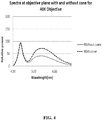
- Table 1 shows the optical output power comparison between illumination paths with and without a cone cavity for same LED.
- Table 1 Peak wavelength /band width 10x/NA0:0.25 20x/ NA:0.8 40x/ NA:0.75 With Cone 545nm/25nm 43 81 33 562nm/40nm 77 146 59 470nm/40nm 40 79 29 628nm/40nm 55 109 44 Without Cone 545nm/25nm 28 68 19 562nm/40nm 50 121 34 470nm/40nm 40 95 26 628nm/40nm 34 85 24 Improvement 545nm/25nm 50% 19% 74% 562nm/40nm 53% 21% 75% 470nm/40nm -1% -17% 11% 628nm/40nm 62% 28% 85%
- the optical power at objective plane of a microscope was improved from 19% to 70% in the green and yellow bands depending on the microscope objective selected. Because the different objectives have different numerical aperture and input diameter, the coupling improvement is variable. For the blue band, the power at the objective plane is increased for 40X but it slight decrease for 10X and 20X because some of the blue light is reflected back onto the phosphor which increases the emission in the green and yellow bands.
- FIG. 5 is a schematic diagram of a second embodiment of an illumination system 500 with increased optical power in the green band.
- the illumination system 500 may include multiple LED light sources 501, where integrating cones 502a, 502b may be coupled with one or more of the multiple LEDs 501a, 501b.
- the LEDs 501a, 501b may have different properties, for example, producing light having of different wavelengths, different beam sizes, and/or different power characteristics.
- the light of the LEDs 501a, 501b and integrating cones 502a, 502b may be combined by a blending means 530, for example, a prism or dichroic plates.
- the combined light may be collimated by a collimating lens 505.
- the collimated beam may be coupled to a microscopy system 507. While FIG. 5 shows two LEDs 501a, 501b and two integrating cones 502a, 502b, alternative embodiments may have two, three, or more LEDs, and two, three or more integrating cones. Furthermore, there is not necessarily a one-to-one relationship between the number of LEDs and the number of integrating cones. For example, a first LED may be coupled with an integrating cone, and a second LED may not be coupled with an integrating cone.
- one or more integrating cones 602a, 602b can also be used in light guide coupled applications to increase the green optical power coupled to a light guide 606.
- the light of the LEDs 601a, 601b and integrating cones 602a, 602b may be combined by blending means 630.
- Collimated light from a collimating lens 604 is coupled to the light guide 606 by using a focus lens 605.
- the output of the light guide 606 may be collimated and coupled to a microscopy system 607 by an optical lens system 610.
- the blending means 630 may include one or more dichroic filters/plates.
- the blending means 630 may also blend in light from light sources in addition to or instead of LED 601a, which may or may not incorporate one or more additional integrating cones.
- FIG. 7 is a flowchart of an exemplary method 700 for increasing the optical power of a solid state light source with a phosphor layer in the green and/or yellow bands for improved fluorescence microscopy.
- any process descriptions or blocks in flowcharts should be understood as representing modules, segments, portions of code, or steps that include one or more instructions for implementing specific logical functions in the process, and alternative implementations are included within the scope of the present invention in which functions may be executed out of order from that shown or discussed, including substantially concurrently or in reverse order, depending on the functionality involved, as would be understood by those reasonably skilled in the art of the present invention. The method is described with reference to FIG. 2 .
- An integrating cone cavity 102 having an input opening 202, an output opening 203, and a reflective interior surface 206 formed between the input opening 202 the output opening 203 is provided, as shown in block 710.
- Substantially blue light from a large area solid state lighting device 101 is received into the input opening 202, as shown by block 720.
- Substantially green and/or yellow light from a phosphor layer 201 on the solid state lighting device 101 is received into the input opening 202, as shown by block 730.
- a first portion of received blue light is directly emitted through the output opening 203, as shown by block 740.
- the reflector interior surface 206 reflects a second portion of the received blue light back to the phosphor layer 201, as shown by block 750.
- the phosphor layer 201 converts at least some of the second portion of the reflected blue light to green and/or yellow light as shown by block 760.
- the received and the converted green and/or yellow light is emitted through the output opening 203 as shown by block 770.
- the embodiments described above offer a balance between cost and performance and for cost limited applications, providing a solution with increased optical power in critical wavelength bands compared to previous solutions.
- the embodiments can be used for directly coupled or light guide coupled illumination products where a larger LED chip is utilized in order to meet the optical power requirements of an application.
- the embodiments may be particularly useful in fluorescence imaging application where it is desirable to have equal power across all visible wavelength bands.
Landscapes
- Physics & Mathematics (AREA)
- General Physics & Mathematics (AREA)
- Optics & Photonics (AREA)
- Engineering & Computer Science (AREA)
- General Engineering & Computer Science (AREA)
- Chemical & Material Sciences (AREA)
- Analytical Chemistry (AREA)
- Health & Medical Sciences (AREA)
- Spectroscopy & Molecular Physics (AREA)
- Nuclear Medicine, Radiotherapy & Molecular Imaging (AREA)
- Biochemistry (AREA)
- General Health & Medical Sciences (AREA)
- Immunology (AREA)
- Pathology (AREA)
- Life Sciences & Earth Sciences (AREA)
- Microscoopes, Condenser (AREA)
- Led Device Packages (AREA)
Claims (12)
- Verfahren zum Steigern der optischen Leistung einer Festkörper-Lichtquelle (101) mit einer Phosphorschicht (201) in den grünen und/oder gelben Bändern für verbesserte Fluoreszenzmikroskopie, das die folgenden Schritte umfasst:Bereitstellen (710) eines integrierenden Kegels (102), der eine Eingangsöffnung (202), eine Ausgangsöffnung (203) und eine reflektierende Innenfläche (206) aufweist, die zwischen der Eingangsöffnung (202) und der Ausgangsöffnung (203) ausgebildet ist;Empfangen (720) im Wesentlichen blauen Lichts von einer Großbereichs-Festkörper-Beleuchtungsvorrichtung (101) in der Eingangsöffnung (202);Empfangen (730) im Wesentlichen grünen und/oder gelben Lichts von der Phosphorschicht (201) in der Eingangsöffnung (202);Senden (740) eines ersten Teils empfangenen blauen Lichts direkt durch die Ausgangsöffnung (203);Reflektieren und Zerstreuen (750), mit der Reflektorinnenfläche (206), eines zweiten Teils des empfangenen blauen Lichts zurück auf die Phosphorschicht (201);Umwandeln (760), mit der Phosphorschicht (201), wenigstens eines Teils des zweiten Teils des reflektierten und zerstreuten blauen Lichts in grünes und/oder gelbes Licht; undSenden (770) des empfangenen und umgewandelten grünen und/oder gelben Lichts durch die Ausgangsöffnung (203).
- System, das aufweist:eine erste Festkörper-Beleuchtungsvorrichtung (101, 501a, 601a) mit einer Phosphorschicht (201), die dazu geeignet ist, blaues Licht in grünes und/oder gelbes Licht umzuwandeln;einen ersten integrierenden Kegel (102, 502a, 602a), der eine Eingangsöffnung (202), eine Ausgangsöffnung (203) und eine reflektierende Innenfläche (206) aufweist, die zwischen der Eingangsöffnung (202) und der Ausgangsöffnung (203) ausgebildet ist, wobei der integrierende Kegel (102, 502a, 602a) dazu konfiguriert ist, Licht von der Festkörper-Beleuchtungsvorrichtung (101, 501a, 601a) und der Phosphorschicht (201) durch die Innenfläche (206) zu empfangen, zu integrieren und umzuformen, und Licht durch die Ausgangsöffnung (203) zu senden,
wobei die Ausgangsöffnung (203) einen kleineren Bereich hat als der Bereich der Eingangsöffnung (202);eine Sammellinse (103), die dazu konfiguriert ist, Licht zu empfangen, das von dem ersten integrierenden Kegel (102, 502a, 602a) ausgesendet wird; undeinen Kollimator (105), der dazu konfiguriert ist, Licht, das von der Sammellinse (103) empfangen wird, zu bündeln. - System nach Anspruch 2, das des Weiteren ein Mikroskopiesystem aufweist, das dazu konfiguriert ist, gebündeltes Licht von dem Kollimator (105) zu empfangen.
- System nach Anspruch 2, wobei die reflektierende Innenfläche (206) dazu konfiguriert ist, sichtbares Licht mit Lambertschen Zerstreuungseigenschaften zu reflektieren.
- System nach Anspruch 2, das des Weiteren aufweist:eine zweite Großbereichs-Festkörper-Beleuchtungsvorrichtung (501b, 601b) mit einer Phosphorschicht;einen zweiten integrierenden Kegel (502b, 602b), der eine Eingangsöffnung, eine Ausgangsöffnung und eine reflektierende Innenfläche aufweist, die zwischen der Eingangsöffnung und der Ausgangsöffnung ausgebildet ist, wobei der integrierende Kegel (502b, 602b) dazu konfiguriert ist, Licht von der Festkörper-Beleuchtungsvorrichtung (501b, 601b) und der Phosphorschicht durch die Innenfläche zu empfangen, zu integrieren und umzuformen, undLicht durch die Ausgangsöffnung zu senden; undeine Kombiniervorrichtung (530, 630), die dazu konfiguriert ist, Licht, das von dem ersten integrierenden Kegel (502a, 602a) und dem zweiten integrierenden Kegel (502b, 602b) ausgesendet wird, zu mischen und gemischtes Licht an die Sammellinse (103) zu leiten.
- System nach Anspruch 5, wobei die zweite Großbereichs-Festkörper-Beleuchtungsvorrichtung (501b, 601b) Beleuchtungseigenschaften hat, die sich von denen der ersten Großbereichs-Festkörper-Beleuchtungsvorrichtung (501a, 601a) unterscheiden.
- System nach Anspruch 6, wobei die zweite Großbereichs-Festkörper-Beleuchtungsvorrichtung (501b, 601b) einen anderen Wellenlängenbereich erzeugt als die erste Großbereichs-Festkörper-Beleuchtungsvorrichtung (501a, 601a).
- System nach Anspruch 2, das des Weiteren einen Lichtleiter (606) aufweist, der zwischen dem Kegel (602a) und einem Ziel angeordnet ist.
- System nach Anspruch 8, wobei der Ausgang des Lichtleiters (606) gebündelt wird und über einen Adapter an ein Mikroskopiesystem (607) gekoppelt wird.
- System nach Anspruch 2, das des Weiteren aufweist:eine zweite Festkörper-Beleuchtungsvorrichtung (501b, 601b), die dazu konfiguriert ist, UV-Licht zu erzeugen; undeine Kombiniervorrichtung (530), die dazu konfiguriert ist, Licht, das von dem ersten integrierenden Kegel (502a, 602a) und der zweiten Festkörper-Beleuchtungsvorrichtung (501b, 601b) ausgesendet wird, zu mischen und gemischtes Licht an die Sammellinse zu leiten.
- System nach Anspruch 10, das des Weiteren eine dritte Festkörper-Beleuchtungsvorrichtung aufweist, die dazu konfiguriert ist, ein Wellenlängenlicht zu erzeugen, das sich von den ersten und zweiten Festkörper-Beleuchtungsvorrichtungen (501a, 501b, 601a, 601b) unterscheidet.
- System nach Anspruch 11, wobei die Kombiniervorrichtung (530, 630) ein(e) dichroitische(s) Filter/Platte aufweist.
Applications Claiming Priority (2)
| Application Number | Priority Date | Filing Date | Title |
|---|---|---|---|
| US14/691,987 US9581314B2 (en) | 2015-04-21 | 2015-04-21 | Integrating cone for an illumination device |
| PCT/US2016/028235 WO2016172074A1 (en) | 2015-04-21 | 2016-04-19 | Integrating cone for an illumination device |
Publications (2)
| Publication Number | Publication Date |
|---|---|
| EP3286593A1 EP3286593A1 (de) | 2018-02-28 |
| EP3286593B1 true EP3286593B1 (de) | 2019-06-12 |
Family
ID=55967419
Family Applications (1)
| Application Number | Title | Priority Date | Filing Date |
|---|---|---|---|
| EP16722452.6A Active EP3286593B1 (de) | 2015-04-21 | 2016-04-19 | Integrationskegel für eine beleuchtungsvorrichtung |
Country Status (3)
| Country | Link |
|---|---|
| US (2) | US9581314B2 (de) |
| EP (1) | EP3286593B1 (de) |
| WO (1) | WO2016172074A1 (de) |
Families Citing this family (3)
| Publication number | Priority date | Publication date | Assignee | Title |
|---|---|---|---|---|
| JP2018040914A (ja) * | 2016-09-07 | 2018-03-15 | ウシオ電機株式会社 | 蛍光顕微鏡用光源装置および蛍光顕微鏡 |
| US20240310617A1 (en) * | 2021-06-30 | 2024-09-19 | Cytoveris Inc. | Method and apparatus for mitigating specular highlights in imaging of biological tissue |
| US12013099B2 (en) * | 2021-12-02 | 2024-06-18 | Lumileds Llc | Projecting a static light pattern or symbol |
Family Cites Families (13)
| Publication number | Priority date | Publication date | Assignee | Title |
|---|---|---|---|---|
| JP2004055819A (ja) | 2002-07-19 | 2004-02-19 | Univ Osaka | レーザ光集光器、及びレーザ光集光方法 |
| TWI332069B (en) | 2006-06-13 | 2010-10-21 | Wavien Inc | Illumination system and method for recycling light to increase the brightness of the light source |
| US8098375B2 (en) | 2007-08-06 | 2012-01-17 | Lumencor, Inc. | Light emitting diode illumination system |
| DE102009055216A1 (de) * | 2009-12-22 | 2011-06-30 | Carl Zeiss Microlmaging GmbH, 07745 | Lumineszenzmikroskopie |
| DE102010028949A1 (de) | 2010-05-12 | 2011-11-17 | Osram Gesellschaft mit beschränkter Haftung | Scheinwerfermodul |
| DE102011012297B4 (de) * | 2011-02-24 | 2022-12-22 | OSRAM Opto Semiconductors Gesellschaft mit beschränkter Haftung | Beleuchtungsvorrichtung |
| US8979316B2 (en) * | 2011-05-11 | 2015-03-17 | Dicon Fiberoptics Inc. | Zoom spotlight using LED array |
| US9239133B2 (en) | 2012-05-24 | 2016-01-19 | Excelitas Canada, Inc. | High brightness solid state illumination system for fluorescence imaging and analysis |
| US20130314893A1 (en) | 2012-05-24 | 2013-11-28 | Lumen Dynamics Group Inc. | High brightness illumination system and wavelength conversion module for microscopy and other applications |
| DE102012212436B4 (de) | 2012-07-16 | 2022-07-14 | Coretronic Corporation | Lichtmodul für eine Projektionsvorrichtung und Verfahren zur Generierung des Blauanteils in einem Lichtmodul für eine Projektionsvorrichtung |
| JP6056117B2 (ja) * | 2012-12-06 | 2017-01-11 | スタンレー電気株式会社 | 発光装置及び車両用灯具 |
| US9250431B2 (en) * | 2013-09-05 | 2016-02-02 | Excelitas Canada, Inc. | Diffusing collection lens for direct coupled high power microscopy illumination systems |
| JP6529713B2 (ja) * | 2013-09-17 | 2019-06-12 | 日亜化学工業株式会社 | 発光装置 |
-
2015
- 2015-04-21 US US14/691,987 patent/US9581314B2/en active Active
-
2016
- 2016-04-19 EP EP16722452.6A patent/EP3286593B1/de active Active
- 2016-04-19 WO PCT/US2016/028235 patent/WO2016172074A1/en not_active Ceased
-
2017
- 2017-02-23 US US15/440,071 patent/US9904045B2/en active Active
Non-Patent Citations (1)
| Title |
|---|
| None * |
Also Published As
| Publication number | Publication date |
|---|---|
| US20160312980A1 (en) | 2016-10-27 |
| US9904045B2 (en) | 2018-02-27 |
| WO2016172074A1 (en) | 2016-10-27 |
| EP3286593A1 (de) | 2018-02-28 |
| US9581314B2 (en) | 2017-02-28 |
| US20170160530A1 (en) | 2017-06-08 |
Similar Documents
| Publication | Publication Date | Title |
|---|---|---|
| CN102901016B (zh) | 光源装置、照明装置、车辆用前照灯和车辆 | |
| CN1993075B (zh) | 光源装置以及备有该光源装置的内视镜 | |
| JP5615355B2 (ja) | 発光ダイオード光エンジン | |
| CN103988502B (zh) | 具有荧光材料元件的照明单元 | |
| CN101283305B (zh) | 具有光学集中器与波长转换元件的照明系统 | |
| CN100381864C (zh) | 光源 | |
| CN102753883B (zh) | 包括磷光体、辐射源、光学系统和散热器的灯 | |
| CN102187478B (zh) | 发光模块、发光模块的制造方法及灯具单元 | |
| US10443800B2 (en) | Laser-based light source with heat conducting outcoupling dome | |
| CN103615671B (zh) | 光源 | |
| US20130329448A1 (en) | Lighting apparatus with phosphor element | |
| TW201708886A (zh) | 用於產生高亮度光的光學裝置 | |
| CN100565872C (zh) | 高亮度发光二极管设备 | |
| EP3286593B1 (de) | Integrationskegel für eine beleuchtungsvorrichtung | |
| JP7416791B2 (ja) | 照明光源及び車両用ライト | |
| US12510229B2 (en) | Light source | |
| CN110906272B (zh) | 一种光源装置及车灯 | |
| CN106922178A (zh) | 发光设备 | |
| CN107525042A (zh) | 磷光板和包括该磷光板的照明装置 | |
| US20210054988A1 (en) | Light conversion devices and lighting devices | |
| WO2025231271A1 (en) | Remote phosphor configuration for high luminance applications |
Legal Events
| Date | Code | Title | Description |
|---|---|---|---|
| STAA | Information on the status of an ep patent application or granted ep patent |
Free format text: STATUS: THE INTERNATIONAL PUBLICATION HAS BEEN MADE |
|
| PUAI | Public reference made under article 153(3) epc to a published international application that has entered the european phase |
Free format text: ORIGINAL CODE: 0009012 |
|
| STAA | Information on the status of an ep patent application or granted ep patent |
Free format text: STATUS: REQUEST FOR EXAMINATION WAS MADE |
|
| 17P | Request for examination filed |
Effective date: 20171114 |
|
| AK | Designated contracting states |
Kind code of ref document: A1 Designated state(s): AL AT BE BG CH CY CZ DE DK EE ES FI FR GB GR HR HU IE IS IT LI LT LU LV MC MK MT NL NO PL PT RO RS SE SI SK SM TR |
|
| AX | Request for extension of the european patent |
Extension state: BA ME |
|
| DAV | Request for validation of the european patent (deleted) | ||
| DAX | Request for extension of the european patent (deleted) | ||
| GRAP | Despatch of communication of intention to grant a patent |
Free format text: ORIGINAL CODE: EPIDOSNIGR1 |
|
| STAA | Information on the status of an ep patent application or granted ep patent |
Free format text: STATUS: GRANT OF PATENT IS INTENDED |
|
| INTG | Intention to grant announced |
Effective date: 20190103 |
|
| GRAS | Grant fee paid |
Free format text: ORIGINAL CODE: EPIDOSNIGR3 |
|
| GRAA | (expected) grant |
Free format text: ORIGINAL CODE: 0009210 |
|
| STAA | Information on the status of an ep patent application or granted ep patent |
Free format text: STATUS: THE PATENT HAS BEEN GRANTED |
|
| AK | Designated contracting states |
Kind code of ref document: B1 Designated state(s): AL AT BE BG CH CY CZ DE DK EE ES FI FR GB GR HR HU IE IS IT LI LT LU LV MC MK MT NL NO PL PT RO RS SE SI SK SM TR |
|
| REG | Reference to a national code |
Ref country code: GB Ref legal event code: FG4D |
|
| REG | Reference to a national code |
Ref country code: CH Ref legal event code: EP |
|
| REG | Reference to a national code |
Ref country code: AT Ref legal event code: REF Ref document number: 1143321 Country of ref document: AT Kind code of ref document: T Effective date: 20190615 |
|
| REG | Reference to a national code |
Ref country code: DE Ref legal event code: R096 Ref document number: 602016015219 Country of ref document: DE |
|
| REG | Reference to a national code |
Ref country code: IE Ref legal event code: FG4D |
|
| REG | Reference to a national code |
Ref country code: NL Ref legal event code: MP Effective date: 20190612 |
|
| REG | Reference to a national code |
Ref country code: LT Ref legal event code: MG4D |
|
| PG25 | Lapsed in a contracting state [announced via postgrant information from national office to epo] |
Ref country code: FI Free format text: LAPSE BECAUSE OF FAILURE TO SUBMIT A TRANSLATION OF THE DESCRIPTION OR TO PAY THE FEE WITHIN THE PRESCRIBED TIME-LIMIT Effective date: 20190612 Ref country code: LT Free format text: LAPSE BECAUSE OF FAILURE TO SUBMIT A TRANSLATION OF THE DESCRIPTION OR TO PAY THE FEE WITHIN THE PRESCRIBED TIME-LIMIT Effective date: 20190612 Ref country code: AL Free format text: LAPSE BECAUSE OF FAILURE TO SUBMIT A TRANSLATION OF THE DESCRIPTION OR TO PAY THE FEE WITHIN THE PRESCRIBED TIME-LIMIT Effective date: 20190612 Ref country code: SE Free format text: LAPSE BECAUSE OF FAILURE TO SUBMIT A TRANSLATION OF THE DESCRIPTION OR TO PAY THE FEE WITHIN THE PRESCRIBED TIME-LIMIT Effective date: 20190612 Ref country code: NO Free format text: LAPSE BECAUSE OF FAILURE TO SUBMIT A TRANSLATION OF THE DESCRIPTION OR TO PAY THE FEE WITHIN THE PRESCRIBED TIME-LIMIT Effective date: 20190912 Ref country code: HR Free format text: LAPSE BECAUSE OF FAILURE TO SUBMIT A TRANSLATION OF THE DESCRIPTION OR TO PAY THE FEE WITHIN THE PRESCRIBED TIME-LIMIT Effective date: 20190612 |
|
| PG25 | Lapsed in a contracting state [announced via postgrant information from national office to epo] |
Ref country code: GR Free format text: LAPSE BECAUSE OF FAILURE TO SUBMIT A TRANSLATION OF THE DESCRIPTION OR TO PAY THE FEE WITHIN THE PRESCRIBED TIME-LIMIT Effective date: 20190913 Ref country code: LV Free format text: LAPSE BECAUSE OF FAILURE TO SUBMIT A TRANSLATION OF THE DESCRIPTION OR TO PAY THE FEE WITHIN THE PRESCRIBED TIME-LIMIT Effective date: 20190612 Ref country code: RS Free format text: LAPSE BECAUSE OF FAILURE TO SUBMIT A TRANSLATION OF THE DESCRIPTION OR TO PAY THE FEE WITHIN THE PRESCRIBED TIME-LIMIT Effective date: 20190612 Ref country code: BG Free format text: LAPSE BECAUSE OF FAILURE TO SUBMIT A TRANSLATION OF THE DESCRIPTION OR TO PAY THE FEE WITHIN THE PRESCRIBED TIME-LIMIT Effective date: 20190912 |
|
| REG | Reference to a national code |
Ref country code: AT Ref legal event code: MK05 Ref document number: 1143321 Country of ref document: AT Kind code of ref document: T Effective date: 20190612 |
|
| PG25 | Lapsed in a contracting state [announced via postgrant information from national office to epo] |
Ref country code: EE Free format text: LAPSE BECAUSE OF FAILURE TO SUBMIT A TRANSLATION OF THE DESCRIPTION OR TO PAY THE FEE WITHIN THE PRESCRIBED TIME-LIMIT Effective date: 20190612 Ref country code: NL Free format text: LAPSE BECAUSE OF FAILURE TO SUBMIT A TRANSLATION OF THE DESCRIPTION OR TO PAY THE FEE WITHIN THE PRESCRIBED TIME-LIMIT Effective date: 20190612 Ref country code: CZ Free format text: LAPSE BECAUSE OF FAILURE TO SUBMIT A TRANSLATION OF THE DESCRIPTION OR TO PAY THE FEE WITHIN THE PRESCRIBED TIME-LIMIT Effective date: 20190612 Ref country code: RO Free format text: LAPSE BECAUSE OF FAILURE TO SUBMIT A TRANSLATION OF THE DESCRIPTION OR TO PAY THE FEE WITHIN THE PRESCRIBED TIME-LIMIT Effective date: 20190612 Ref country code: PT Free format text: LAPSE BECAUSE OF FAILURE TO SUBMIT A TRANSLATION OF THE DESCRIPTION OR TO PAY THE FEE WITHIN THE PRESCRIBED TIME-LIMIT Effective date: 20191014 Ref country code: AT Free format text: LAPSE BECAUSE OF FAILURE TO SUBMIT A TRANSLATION OF THE DESCRIPTION OR TO PAY THE FEE WITHIN THE PRESCRIBED TIME-LIMIT Effective date: 20190612 Ref country code: SK Free format text: LAPSE BECAUSE OF FAILURE TO SUBMIT A TRANSLATION OF THE DESCRIPTION OR TO PAY THE FEE WITHIN THE PRESCRIBED TIME-LIMIT Effective date: 20190612 |
|
| PG25 | Lapsed in a contracting state [announced via postgrant information from national office to epo] |
Ref country code: SM Free format text: LAPSE BECAUSE OF FAILURE TO SUBMIT A TRANSLATION OF THE DESCRIPTION OR TO PAY THE FEE WITHIN THE PRESCRIBED TIME-LIMIT Effective date: 20190612 Ref country code: IT Free format text: LAPSE BECAUSE OF FAILURE TO SUBMIT A TRANSLATION OF THE DESCRIPTION OR TO PAY THE FEE WITHIN THE PRESCRIBED TIME-LIMIT Effective date: 20190612 Ref country code: IS Free format text: LAPSE BECAUSE OF FAILURE TO SUBMIT A TRANSLATION OF THE DESCRIPTION OR TO PAY THE FEE WITHIN THE PRESCRIBED TIME-LIMIT Effective date: 20191012 Ref country code: ES Free format text: LAPSE BECAUSE OF FAILURE TO SUBMIT A TRANSLATION OF THE DESCRIPTION OR TO PAY THE FEE WITHIN THE PRESCRIBED TIME-LIMIT Effective date: 20190612 |
|
| REG | Reference to a national code |
Ref country code: DE Ref legal event code: R097 Ref document number: 602016015219 Country of ref document: DE |
|
| PG25 | Lapsed in a contracting state [announced via postgrant information from national office to epo] |
Ref country code: TR Free format text: LAPSE BECAUSE OF FAILURE TO SUBMIT A TRANSLATION OF THE DESCRIPTION OR TO PAY THE FEE WITHIN THE PRESCRIBED TIME-LIMIT Effective date: 20190612 |
|
| PLBE | No opposition filed within time limit |
Free format text: ORIGINAL CODE: 0009261 |
|
| STAA | Information on the status of an ep patent application or granted ep patent |
Free format text: STATUS: NO OPPOSITION FILED WITHIN TIME LIMIT |
|
| PG25 | Lapsed in a contracting state [announced via postgrant information from national office to epo] |
Ref country code: DK Free format text: LAPSE BECAUSE OF FAILURE TO SUBMIT A TRANSLATION OF THE DESCRIPTION OR TO PAY THE FEE WITHIN THE PRESCRIBED TIME-LIMIT Effective date: 20190612 Ref country code: PL Free format text: LAPSE BECAUSE OF FAILURE TO SUBMIT A TRANSLATION OF THE DESCRIPTION OR TO PAY THE FEE WITHIN THE PRESCRIBED TIME-LIMIT Effective date: 20190612 |
|
| 26N | No opposition filed |
Effective date: 20200313 |
|
| PG25 | Lapsed in a contracting state [announced via postgrant information from national office to epo] |
Ref country code: SI Free format text: LAPSE BECAUSE OF FAILURE TO SUBMIT A TRANSLATION OF THE DESCRIPTION OR TO PAY THE FEE WITHIN THE PRESCRIBED TIME-LIMIT Effective date: 20190612 Ref country code: IS Free format text: LAPSE BECAUSE OF FAILURE TO SUBMIT A TRANSLATION OF THE DESCRIPTION OR TO PAY THE FEE WITHIN THE PRESCRIBED TIME-LIMIT Effective date: 20200224 |
|
| PG2D | Information on lapse in contracting state deleted |
Ref country code: IS |
|
| PG25 | Lapsed in a contracting state [announced via postgrant information from national office to epo] |
Ref country code: MC Free format text: LAPSE BECAUSE OF FAILURE TO SUBMIT A TRANSLATION OF THE DESCRIPTION OR TO PAY THE FEE WITHIN THE PRESCRIBED TIME-LIMIT Effective date: 20190612 |
|
| REG | Reference to a national code |
Ref country code: CH Ref legal event code: PL |
|
| PG25 | Lapsed in a contracting state [announced via postgrant information from national office to epo] |
Ref country code: CH Free format text: LAPSE BECAUSE OF NON-PAYMENT OF DUE FEES Effective date: 20200430 Ref country code: LI Free format text: LAPSE BECAUSE OF NON-PAYMENT OF DUE FEES Effective date: 20200430 Ref country code: FR Free format text: LAPSE BECAUSE OF NON-PAYMENT OF DUE FEES Effective date: 20200430 Ref country code: LU Free format text: LAPSE BECAUSE OF NON-PAYMENT OF DUE FEES Effective date: 20200419 |
|
| REG | Reference to a national code |
Ref country code: BE Ref legal event code: MM Effective date: 20200430 |
|
| PG25 | Lapsed in a contracting state [announced via postgrant information from national office to epo] |
Ref country code: BE Free format text: LAPSE BECAUSE OF NON-PAYMENT OF DUE FEES Effective date: 20200430 |
|
| PG25 | Lapsed in a contracting state [announced via postgrant information from national office to epo] |
Ref country code: IE Free format text: LAPSE BECAUSE OF NON-PAYMENT OF DUE FEES Effective date: 20200419 |
|
| PG25 | Lapsed in a contracting state [announced via postgrant information from national office to epo] |
Ref country code: MT Free format text: LAPSE BECAUSE OF FAILURE TO SUBMIT A TRANSLATION OF THE DESCRIPTION OR TO PAY THE FEE WITHIN THE PRESCRIBED TIME-LIMIT Effective date: 20190612 Ref country code: CY Free format text: LAPSE BECAUSE OF FAILURE TO SUBMIT A TRANSLATION OF THE DESCRIPTION OR TO PAY THE FEE WITHIN THE PRESCRIBED TIME-LIMIT Effective date: 20190612 |
|
| PG25 | Lapsed in a contracting state [announced via postgrant information from national office to epo] |
Ref country code: MK Free format text: LAPSE BECAUSE OF FAILURE TO SUBMIT A TRANSLATION OF THE DESCRIPTION OR TO PAY THE FEE WITHIN THE PRESCRIBED TIME-LIMIT Effective date: 20190612 |
|
| P01 | Opt-out of the competence of the unified patent court (upc) registered |
Effective date: 20230510 |
|
| PGFP | Annual fee paid to national office [announced via postgrant information from national office to epo] |
Ref country code: DE Payment date: 20250429 Year of fee payment: 10 |
|
| PGFP | Annual fee paid to national office [announced via postgrant information from national office to epo] |
Ref country code: GB Payment date: 20250428 Year of fee payment: 10 |