EP3287821A1 - Verjüngter wellenleiter und siliciumbasierter chip - Google Patents
Verjüngter wellenleiter und siliciumbasierter chip Download PDFInfo
- Publication number
- EP3287821A1 EP3287821A1 EP15891572.8A EP15891572A EP3287821A1 EP 3287821 A1 EP3287821 A1 EP 3287821A1 EP 15891572 A EP15891572 A EP 15891572A EP 3287821 A1 EP3287821 A1 EP 3287821A1
- Authority
- EP
- European Patent Office
- Prior art keywords
- waveguide
- shallow
- etched strip
- tapered
- etched
- Prior art date
- Legal status (The legal status is an assumption and is not a legal conclusion. Google has not performed a legal analysis and makes no representation as to the accuracy of the status listed.)
- Granted
Links
Images


Classifications
-
- G—PHYSICS
- G02—OPTICS
- G02B—OPTICAL ELEMENTS, SYSTEMS OR APPARATUS
- G02B6/00—Light guides; Structural details of arrangements comprising light guides and other optical elements, e.g. couplings
- G02B6/10—Light guides; Structural details of arrangements comprising light guides and other optical elements, e.g. couplings of the optical waveguide type
- G02B6/12—Light guides; Structural details of arrangements comprising light guides and other optical elements, e.g. couplings of the optical waveguide type of the integrated circuit kind
- G02B6/122—Basic optical elements, e.g. light-guiding paths
- G02B6/1228—Tapered waveguides, e.g. integrated spot-size transformers
-
- G—PHYSICS
- G02—OPTICS
- G02B—OPTICAL ELEMENTS, SYSTEMS OR APPARATUS
- G02B6/00—Light guides; Structural details of arrangements comprising light guides and other optical elements, e.g. couplings
- G02B6/10—Light guides; Structural details of arrangements comprising light guides and other optical elements, e.g. couplings of the optical waveguide type
- G02B6/12—Light guides; Structural details of arrangements comprising light guides and other optical elements, e.g. couplings of the optical waveguide type of the integrated circuit kind
- G02B2006/12035—Materials
- G02B2006/12061—Silicon
-
- G—PHYSICS
- G02—OPTICS
- G02B—OPTICAL ELEMENTS, SYSTEMS OR APPARATUS
- G02B6/00—Light guides; Structural details of arrangements comprising light guides and other optical elements, e.g. couplings
- G02B6/10—Light guides; Structural details of arrangements comprising light guides and other optical elements, e.g. couplings of the optical waveguide type
- G02B6/12—Light guides; Structural details of arrangements comprising light guides and other optical elements, e.g. couplings of the optical waveguide type of the integrated circuit kind
- G02B2006/12083—Constructional arrangements
- G02B2006/12097—Ridge, rib or the like
-
- G—PHYSICS
- G02—OPTICS
- G02B—OPTICAL ELEMENTS, SYSTEMS OR APPARATUS
- G02B6/00—Light guides; Structural details of arrangements comprising light guides and other optical elements, e.g. couplings
- G02B6/10—Light guides; Structural details of arrangements comprising light guides and other optical elements, e.g. couplings of the optical waveguide type
- G02B6/12—Light guides; Structural details of arrangements comprising light guides and other optical elements, e.g. couplings of the optical waveguide type of the integrated circuit kind
- G02B2006/12083—Constructional arrangements
- G02B2006/121—Channel; buried or the like
Definitions
- the present invention relates to the field of communications technologies, and in particular, to a tapered waveguide and a silicon-based chip.
- Silicon-based optoelectronics as a mainstream technology in all-optical signal processing, is used to dispose devices such as a laser, a modulator, a detector, and an optical switch together onto a silicon-on-insulator (SOI) material to form a silicon-based chip. Due to advantages of high bandwidth, low power consumption, and being compatible with an existing CMOS technology, a silicon-based optical chip is a development direction and a key technology of all-optical switching in the future.
- SOI silicon-on-insulator
- a waveguide is a most basic structure in the silicon-based chip, and is configured to connect and form various devices.
- the waveguide includes a core layer made of a high-refractive-index material and a buried cladding and an upper cladding that are made of low-refractive-index materials.
- a base of the chip is usually a silicon base.
- a channel waveguide and a ridge waveguide are two common types of waveguides in a silicon-based chip.
- the channel waveguide has a channel core section, as shown in FIG. 2 , and is mostly used to connect various devices.
- the ridge waveguide includes a central waveguide 1 with a higher height and shallow-etched strip waveguides 2 with a lower height on both sides, as shown in FIG. 3 , and is mostly used in functional devices.
- the ridge waveguide may be used in an MMI, a DC (directional coupler), a PBS (polarization beam splitter), a PR (polarization rotator), an optical switch, and a modulator (a PN junction waveguide is a ridge waveguide).
- a tapered waveguide needs to be used to connect the channel waveguide and the ridge waveguide. Therefore, the tapered waveguide is also a basic device widely used in the silicon-based chip.
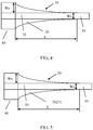
- An existing tapered waveguide connecting a channel waveguide and a ridge waveguide employs a straight-line structure, that is, a width of the tapered waveguide uniformly increases with a length of the tapered waveguide.
- a tapered waveguide of a straight-line structure is shown in FIG. 1 .
- the tapered waveguide includes a base 4, a buried cladding 3 disposed on the base 4, a central waveguide 1, shallow-etched strip waveguides 2, and an upper cladding 5 that encloses the central waveguide 1 and the shallow-etched strip waveguides 2.
- the shallow-etched strip waveguides 2 are symmetrically disposed on both sides of the central waveguide.
- a width of the tapered waveguide is equal to a sum of widths of the ridge waveguides on both sides and a width of the central waveguide.
- the widths of the shallow-etched strip waveguides and a length of the tapered waveguide have a linear relationship, while an effective refractive index of the waveguide and the widths of the shallow-etched strip waveguides do not have a linear relationship. Therefore, the effective refractive index of the waveguide and the length of the tapered waveguide do not have a linear relationship.
- a narrower area (for example, 0 to 0.3 ⁇ m) of the shallow-etched strip waveguide accounts for a smaller portion of the overall length, but its corresponding effective refractive index changes greatly, resulting in a relatively large insertion loss.
- a wider area (for example, 0.3 to 1 ⁇ m) of the shallow-etched strip waveguide accounts for a larger portion of the overall length, but the effective refractive index does not change greatly, so that the insertion loss of the device cannot be reduced but the length of the device is increased.
- Disadvantage 1 A narrower area of a shallow-etched strip waveguide has a shorter length, but an effective refractive index changes dramatically, resulting in a relatively large insertion loss of the device.
- Disadvantage 2 A wider area of the shallow-etched strip waveguide has a longer length, but the effective refractive index does not change significantly. This cannot reduce a loss obviously, but increases an overall length of the device.
- the present invention provides a tapered waveguide and a silicon-based chip to reduce a loss and a length of the tapered waveguide.
- a tapered waveguide includes a central waveguide and shallow-etched strip waveguides disposed on both sides of the central waveguide, where each shallow-etched strip waveguide is of a structure with a gradually changing width, and an outline of a side, away from the central waveguide and in a length direction, of the shallow-etched strip waveguide is a concave arc.
- a variation relationship between a width of the shallow-etched strip waveguide and a length of the tapered waveguide conforms to a rule that an effective refractive index of the tapered waveguide uniformly changes with a length of the tapered waveguide.
- a variation relationship between a width of the shallow-etched strip waveguide of the tapered waveguide and a length of the shallow-etched strip waveguide satisfies a parabolic equation.
- a variation relationship between a width of the shallow-etched strip waveguide of the tapered waveguide and a length of the shallow-etched strip waveguide satisfies an elliptic equation.
- the tapered waveguide further includes a buried cladding bearing the central waveguide and the shallow-etched strip waveguides, and an upper cladding enclosing the central waveguide and the shallow-etched strip waveguides, where refractive indexes of the buried cladding and the upper cladding are lower than refractive indexes of the central waveguide and the shallow-etched strip waveguides.
- the central waveguide and the shallow-etched strip waveguides are made of silicon, silicon nitride, a polymer, or a semiconductor material.
- the buried cladding and the upper cladding are made of silicon dioxide, silicon nitride, or a boron-doped, phosphorous-doped, or germanium-doped glass material.
- a height of the central waveguide is greater than that of the shallow-etched strip waveguide.
- a silicon-based chip is provided, where the silicon-based chip includes the tapered waveguide according to any one of the foregoing first aspect or the possible implementations.
- a structure of a tapered waveguide is optimized by using a channel central waveguide and concave shallow-etched strip waveguides.
- a narrower area of the shallow-etched strip waveguide has a longer length, so that an effective refractive index changes slowly and an insertion loss of the device can be effectively reduced.
- a wider area of the shallow-etched strip waveguide has a shorter length.
- the effective refractive index barely changes, the insertion loss of the device is not increased, and a length of the device is effectively reduced, thereby facilitating miniaturization of the device.
- FIG. 4 shows a tapered waveguide provided in the present invention
- FIG. 5 , FIG. 6, and FIG. 7 show tapered waveguides of different structures provided in the embodiments.
- a shallow-etched strip waveguide provided in the embodiments may also be referred to as a shallow-etched waveguide, a shallow-etched strip-shaped waveguide, a shallow-etched thin-film waveguide, or a shallow-etched slab waveguide.
- English names of other waveguides in the embodiments are as follows: a channel waveguide (ridge waveguide), a ridge waveguide (rib waveguide), a central waveguide (core waveguide), a shallow-etched strip waveguide (slab waveguide), an upper cladding (upper cladding), and a buried cladding (buried cladding).
- An embodiment of the present invention provides a tapered waveguide 50.
- the tapered waveguide 50 includes a central waveguide 10 and shallow-etched strip waveguides 20 disposed on both sides of the central waveguide 10.
- Each shallow-etched strip waveguide 20 is of a structure with a gradually changing width, and an outline, away from the central waveguide 10 and in a length direction, of the shallow-etched strip waveguide 20 is a concave arc without an abrupt change.
- a wider end of the tapered waveguide is connected to a channel waveguide 30, and a narrower end is connected to a ridge waveguide 40.
- “concave” in the foregoing “concave arc” means that the arc curves inwards towards the waveguide itself.
- the tapered waveguide includes the central waveguide 10 and the shallow-etched strip waveguides 20, and also includes a buried cladding bearing the central waveguide 10 and the shallow-etched strip waveguides 20, and an upper cladding enclosing the central waveguide 10 and the shallow-etched strip waveguides 20. Refractive indexes of the buried cladding and the upper cladding are lower than refractive indexes of the central waveguide 10 and the shallow-etched strip waveguides 20.
- a refractive index refers to a property of a material, that is, changes of a refractive index for rays of a same wavelength.
- the central waveguide 10 and the shallow-etched strip waveguides 20 are made of a material of a high refractive index, while the buried cladding and the upper cladding are made of a material of a low refractive index.
- the central waveguide 10 and the shallow-etched strip waveguides 20 may be made of silicon, silicon nitride, a polymer, or a semiconductor material.
- the buried cladding and the upper cladding may be made of silicon dioxide, silicon nitride, or a boron-doped, phosphorous-doped, or germanium-doped glass material.
- a fraction of boron, phosphorous, or germanium elements doped in the glass material may be a conventional fraction in the prior art, and no limitation is set thereto.
- a height of the central waveguide 10 is greater than that of the shallow-etched strip waveguide 20.
- the central waveguide 10 is located at a center line of the tapered waveguide 50.
- the shallow-etched strip waveguides 20 located on both sides of the central waveguide 10 are centrally symmetric.
- An effective refractive index is an important and common parameter for an optical waveguide. Its value is related to a cross sectional shape of the waveguide and a refractive index of a material of the waveguide. Once the cross sectional shape and material of the waveguide are determined, the effective refractive index of the waveguide is also determined. A specific value can be obtained through calculation by using emulation software. The value of the effective refractive index is related to a mode of the waveguide, and different modes are corresponding to different effective refractive indexes.
- the effective refractive index mentioned in this patent refers to an effective refractive index of a tapered waveguide fundamental mode. A fundamental mode of a waveguide refers to a TE zero-order mode, TE0 for short, in the waveguide.
- the effective refractive index refers to an effective refractive index corresponding to a working wavelength of the tapered waveguide.
- FIG. 8 shows a diagram of a correspondence between a width of a shallow-etched strip waveguide and an effective refractive index.
- a corresponding central waveguide has a width of 0.5 ⁇ m. It can be learned from FIG. 8 that as the width of the shallow-etched strip waveguide increases, the effective refractive index changes. In addition, a smaller width of the shallow-etched strip waveguide 20 indicates a greater change of the effective refractive index. When the width of the shallow-etched strip waveguide 20 is greater than about 0.5 to 1 ⁇ m, the effective refractive index of a waveguide no longer changes obviously.
- a loss of a tapered waveguide mainly comes from mode mismatch, surface roughness of the silicon waveguide, and an absorption loss of the waveguide when light is transmitted through the waveguide.
- the latter two are determined by a manufacturing process and a material of the waveguide, and are irrelevant to a structure of the tapered waveguide itself. Therefore, for the mode mismatch, the structure and a shape of the tapered waveguide can be optimized to reduce an insertion loss. Therefore, in the tapered waveguide provided in this embodiment, a structure of a shallow-etched strip waveguide 20 is optimized by using a concave shallow-etched strip waveguide 20. A narrower area of the shallow-etched strip waveguide has a longer length, so that an effective refractive index changes slowly and an insertion loss of the device can be effectively reduced.
- a wider area of the shallow-etched strip waveguide has a shorter length (that is, a length of a wider part of the shallow-etched strip waveguide is shorter than a length of a narrower part of the shallow-etched strip waveguide).
- the effective refractive index barely changes, the insertion loss of the device is not increased, and a length of the device is effectively reduced, thereby facilitating miniaturization of the device.
- a function f(x) w of the width w and a length x of the shallow-etched strip waveguide satisfies f'(x) > 0 (a second derivative of the function is greater than 0).
- a tapered waveguide provided in this embodiment includes a central waveguide 10, shallow-etched strip waveguides 21, and a buried cladding and an upper cladding that enclose the central waveguide 10 and the shallow-etched strip waveguides 21. Materials of and a location relationship between the parts are the same as those of the tapered waveguide provided in the general embodiment, and details are not described again herein.
- a variation relationship between a width of the shallow-etched strip waveguide 21 of the tapered waveguide provided in this embodiment and a length of the shallow-etched strip waveguide 21 conforms to a rule that an effective refractive index of the waveguide uniformly changes with a length of the waveguide.
- Effective refractive indexes of a ridge waveguide 40 and a channel waveguide 30 are n1 and n2, respectively.
- the effective refractive index at any length x (which is calculated from an end, connected to the channel waveguide 30, of the tapered waveguide 50) can be derived: n2 + x/L * (n1 - n2).
- the corresponding width of the shallow-etched strip waveguide 21 can be obtained, so as to obtain line shapes, in the length direction, of the shallow-etched strip waveguides 21 of the tapered waveguide.
- a width of the central waveguide 10 is Wc
- a width of one of the shallow-etched strip waveguides 20 on both sides are w (that is, a width of a part, on one side of the central waveguide 10, of the tapered waveguide 50, and a value of the width varies with a length of the shallow-etched strip waveguide).
- a total width of the tapered waveguide is Wc + w * 2
- a length of the tapered waveguide is L.
- Two ends of the tapered waveguide are connected to a channel waveguide 30 and a ridge waveguide 40, respectively.
- a width of the channel waveguide 30 is Wc, and a width of the ridge waveguide 40 is Wc + Ws * 2 (widths of shallow-etched strip waveguides on two sides are Ws, and a width of a central waveguide is Wc).
- materials of and a location relationship among a buried cladding, an upper cladding, a central waveguide 10, and shallow-etched strip waveguides 22 of a tapered waveguide provided in this embodiment are the same as those of the tapered waveguide provided in the general embodiment, and details are not described again herein.
- linearity of the shallow-etched strip waveguide 22 of the tapered waveguide provided in this embodiment is changed.
- FIG. 6 shows a relationship between a line shape of the tapered waveguide and a parabola.
- materials of and a location relationship among a buried cladding, an upper cladding, a central waveguide 10, and shallow-etched strip waveguides 23 of a tapered waveguide provided in this embodiment are the same as those of the tapered waveguide provided in the general embodiment, and details are not described again herein.
- a line shape of the shallow-etched strip waveguide 23 of the tapered waveguide provided in this embodiment is changed.
- FIG. 7 shows a relationship between a line shape of the tapered waveguide and an ellipse.
- line shapes of a shallow-etched strip waveguide of the tapered waveguide provided in the embodiments may be different concave arcs.
- Specific line shapes are not limited to the line shapes provided in Embodiment 1, Embodiment 2, and Embodiment 3, and other shapes may also be used.
- a straight-line type is a structure used by a tapered waveguide in the prior art.
- a concave type is a structure of a tapered waveguide provided according to the present invention.
- a difference in concave type 1 and concave type 2 is used concave line shapes. It should be noted that the concave line shapes are not corresponding to that of Embodiment 1 and Embodiment 2.
- a convex type is a structure similar to that of the tapered waveguide provided in this embodiment.
- a loss of a tapered waveguide with the concave type is generally smaller than that of a tapered waveguide with the straight-line type, and a loss of a tapered waveguide with the convex type is the largest. This is the same as the foregoing analysis result. For tapered waveguides with a same length, a loss can be greatly reduced by using a concave structure.
- the tapered waveguide provided in this embodiment can significantly reduce an insertion loss and a length of the device, and increase chip integration.
- the device of the tapered waveguide provided in this embodiment has a simple structure, is compatible with a CMOS technology, is easy to integrate, and has a relatively low process requirement and a relatively high tolerance to process errors.
- An embodiment of the present invention further provides a silicon-based chip, where the silicon-based chip includes the tapered waveguide according to any one of the foregoing embodiments.
- the silicon-based chip provided in this embodiment includes any one of the foregoing tapered waveguides, and has the structure and the effect of the foregoing tapered waveguides. That is, a channel central waveguide and concave shallow-etched strip waveguides are used. A narrower area of the shallow-etched strip waveguide has a longer length, so that an effective refractive index changes slowly and an insertion loss of the device can be effectively reduced. In addition, a wider area of the shallow-etched strip waveguide has a shorter length. However, because the effective refractive index barely changes, the insertion loss of the device is not increased, and a length of the device is effectively reduced, thereby facilitating miniaturization of the device.
Landscapes
- Engineering & Computer Science (AREA)
- Physics & Mathematics (AREA)
- Power Engineering (AREA)
- Microelectronics & Electronic Packaging (AREA)
- General Physics & Mathematics (AREA)
- Optics & Photonics (AREA)
- Optical Integrated Circuits (AREA)
Applications Claiming Priority (2)
| Application Number | Priority Date | Filing Date | Title |
|---|---|---|---|
| CN2015078536 | 2015-05-08 | ||
| PCT/CN2015/080909 WO2016179869A1 (zh) | 2015-05-08 | 2015-06-05 | 一种锥形波导及硅基芯片 |
Publications (3)
| Publication Number | Publication Date |
|---|---|
| EP3287821A1 true EP3287821A1 (de) | 2018-02-28 |
| EP3287821A4 EP3287821A4 (de) | 2018-05-16 |
| EP3287821B1 EP3287821B1 (de) | 2023-09-27 |
Family
ID=57248425
Family Applications (1)
| Application Number | Title | Priority Date | Filing Date |
|---|---|---|---|
| EP15891572.8A Active EP3287821B1 (de) | 2015-05-08 | 2015-06-05 | Verjüngter wellenleiter und siliciumbasierter chip |
Country Status (3)
| Country | Link |
|---|---|
| EP (1) | EP3287821B1 (de) |
| CN (1) | CN107924024B (de) |
| WO (1) | WO2016179869A1 (de) |
Cited By (1)
| Publication number | Priority date | Publication date | Assignee | Title |
|---|---|---|---|---|
| EP3629068A4 (de) * | 2017-06-16 | 2020-06-03 | Huawei Technologies Co., Ltd. | Optischer add-/drop-multiplexer |
Families Citing this family (2)
| Publication number | Priority date | Publication date | Assignee | Title |
|---|---|---|---|---|
| WO2023272690A1 (zh) * | 2021-07-01 | 2023-01-05 | 深圳市速腾聚创科技有限公司 | 脊形波导、微环谐振器、可调光延迟线及芯片 |
| CN114114537B (zh) * | 2021-12-08 | 2022-11-01 | 南通大学 | 一种超紧凑绝热锥形波导的设计方法 |
Family Cites Families (11)
| Publication number | Priority date | Publication date | Assignee | Title |
|---|---|---|---|---|
| US6310995B1 (en) * | 1998-11-25 | 2001-10-30 | University Of Maryland | Resonantly coupled waveguides using a taper |
| KR100293954B1 (ko) * | 1999-05-11 | 2001-06-15 | 윤종용 | 평탄한 주파수 응답을 가진 저손실 광파장 분할기 |
| US20080044126A1 (en) * | 2003-08-04 | 2008-02-21 | Raffaella Costa | Integrated Optical Waveguide Structure with Low Coupling Losses to an External Optical Field |
| CN1271765C (zh) * | 2004-04-02 | 2006-08-23 | 华中科技大学 | 一种集成模斑变换器的脊型波导偏振无关半导体光放大器 |
| US20060133754A1 (en) * | 2004-12-21 | 2006-06-22 | Vipulkumar Patel | Ultra low-loss CMOS compatible silicon waveguides |
| US7532784B2 (en) * | 2006-07-31 | 2009-05-12 | Onechip Photonics Inc. | Integrated vertical wavelength (de)multiplexer |
| CN101881861A (zh) * | 2010-06-13 | 2010-11-10 | 中国科学院半导体研究所 | 非直线锥形倒锥耦合器结构 |
| JP5413865B1 (ja) * | 2012-12-27 | 2014-02-12 | 株式会社フジクラ | 光導波路素子及び光変調器 |
| SG11201510495TA (en) * | 2013-06-27 | 2016-01-28 | Fujikura Ltd | High-order polarization conversion element, optical waveguide element, and dp-qpsk modulator |
| JP5773552B2 (ja) * | 2013-09-20 | 2015-09-02 | 沖電気工業株式会社 | 光素子の製造方法及び光素子 |
| CN104051602B (zh) * | 2014-06-30 | 2017-03-01 | 重庆大学 | 一种脊形波导结构及超辐射发光二极管 |
-
2015
- 2015-06-05 CN CN201580077733.8A patent/CN107924024B/zh active Active
- 2015-06-05 EP EP15891572.8A patent/EP3287821B1/de active Active
- 2015-06-05 WO PCT/CN2015/080909 patent/WO2016179869A1/zh not_active Ceased
Cited By (2)
| Publication number | Priority date | Publication date | Assignee | Title |
|---|---|---|---|---|
| EP3629068A4 (de) * | 2017-06-16 | 2020-06-03 | Huawei Technologies Co., Ltd. | Optischer add-/drop-multiplexer |
| US10871615B2 (en) | 2017-06-16 | 2020-12-22 | Huawei Technologies Co., Ltd. | Optical add/drop multiplexer |
Also Published As
| Publication number | Publication date |
|---|---|
| CN107924024A (zh) | 2018-04-17 |
| EP3287821B1 (de) | 2023-09-27 |
| WO2016179869A1 (zh) | 2016-11-17 |
| EP3287821A4 (de) | 2018-05-16 |
| CN107924024B (zh) | 2020-10-16 |
Similar Documents
| Publication | Publication Date | Title |
|---|---|---|
| CN108885307B (zh) | 用于光子芯片的具有可控模场的光学边缘耦合器 | |
| US11215755B2 (en) | Low loss, polarization-independent, large bandwidth mode converter for edge coupling | |
| JP5728140B1 (ja) | 高次偏波変換素子、光導波路素子、及びdp−qpsk変調器 | |
| US9869816B2 (en) | Light combining/dividing element and light modulator | |
| EP3314320B1 (de) | Modenwandler mit s-gebogener verjüngung und verwandter polarisationsrotator | |
| US9297956B2 (en) | Optical device, optical transmitter, optical receiver, optical transceiver, and method of manufacturing optical device | |
| EP3164746B1 (de) | Optischer koppler mit doppelspitze | |
| US11460635B2 (en) | Optical waveguide device | |
| CN105683793A (zh) | 光功率分离器 | |
| US20200310028A1 (en) | Curved waveguide configuration | |
| EP3287821B1 (de) | Verjüngter wellenleiter und siliciumbasierter chip | |
| EP3203282B1 (de) | Rippenartiger optischer wellenleiter und optischer multiplexer/demultiplexer mit verwendung davon | |
| JP2015169766A (ja) | 偏波回転回路 | |
| GB2396705A (en) | Optical coupler with three waveguides and two gratings | |
| US11662522B2 (en) | Optical waveguide device operated as mode converter | |
| US20200142130A1 (en) | Adjustable Wide-Spectrum Wavelength-Insensitive Directional Coupler | |
| De Heyn et al. | High-performance low-loss silicon-on-insulator microring resonators using TM-polarized light | |
| D’Mello et al. | Numerical Analysis and Optimization of a Multi-Mode Interference Based Polarization Beam Splitter | |
| Navalakhe et al. | Design of low-loss compact 90° bend optical waveguide for photonic circuit applications in SOI platform | |
| Aalto et al. | Si photonics using micron-size waveguides | |
| US20120134633A1 (en) | Connecting channel | |
| Shrestha et al. | Silicon nitride waveguide router enabling directional power transmission | |
| De Heyn et al. | Improved intrinsic Q of Silicon-on-Insulator microring resonators using TM-polarized light | |
| de Melo et al. | Compact SOI Waveguide Crossing for TE 0 and TE 1 Modes | |
| Tanaka et al. | Comparative simulation of three types of 3-dB coupler using a Si wire waveguide |
Legal Events
| Date | Code | Title | Description |
|---|---|---|---|
| STAA | Information on the status of an ep patent application or granted ep patent |
Free format text: STATUS: THE INTERNATIONAL PUBLICATION HAS BEEN MADE |
|
| PUAI | Public reference made under article 153(3) epc to a published international application that has entered the european phase |
Free format text: ORIGINAL CODE: 0009012 |
|
| STAA | Information on the status of an ep patent application or granted ep patent |
Free format text: STATUS: REQUEST FOR EXAMINATION WAS MADE |
|
| 17P | Request for examination filed |
Effective date: 20171122 |
|
| AK | Designated contracting states |
Kind code of ref document: A1 Designated state(s): AL AT BE BG CH CY CZ DE DK EE ES FI FR GB GR HR HU IE IS IT LI LT LU LV MC MK MT NL NO PL PT RO RS SE SI SK SM TR |
|
| AX | Request for extension of the european patent |
Extension state: BA ME |
|
| A4 | Supplementary search report drawn up and despatched |
Effective date: 20180412 |
|
| RIC1 | Information provided on ipc code assigned before grant |
Ipc: G02B 6/122 20060101ALI20180406BHEP Ipc: G02B 6/30 20060101ALI20180406BHEP Ipc: G02B 6/12 20060101AFI20180406BHEP |
|
| DAV | Request for validation of the european patent (deleted) | ||
| DAX | Request for extension of the european patent (deleted) | ||
| STAA | Information on the status of an ep patent application or granted ep patent |
Free format text: STATUS: EXAMINATION IS IN PROGRESS |
|
| 17Q | First examination report despatched |
Effective date: 20210519 |
|
| GRAP | Despatch of communication of intention to grant a patent |
Free format text: ORIGINAL CODE: EPIDOSNIGR1 |
|
| STAA | Information on the status of an ep patent application or granted ep patent |
Free format text: STATUS: GRANT OF PATENT IS INTENDED |
|
| INTG | Intention to grant announced |
Effective date: 20230504 |
|
| GRAS | Grant fee paid |
Free format text: ORIGINAL CODE: EPIDOSNIGR3 |
|
| GRAA | (expected) grant |
Free format text: ORIGINAL CODE: 0009210 |
|
| STAA | Information on the status of an ep patent application or granted ep patent |
Free format text: STATUS: THE PATENT HAS BEEN GRANTED |
|
| AK | Designated contracting states |
Kind code of ref document: B1 Designated state(s): AL AT BE BG CH CY CZ DE DK EE ES FI FR GB GR HR HU IE IS IT LI LT LU LV MC MK MT NL NO PL PT RO RS SE SI SK SM TR |
|
| REG | Reference to a national code |
Ref country code: GB Ref legal event code: FG4D |
|
| REG | Reference to a national code |
Ref country code: CH Ref legal event code: EP |
|
| REG | Reference to a national code |
Ref country code: DE Ref legal event code: R096 Ref document number: 602015085885 Country of ref document: DE |
|
| REG | Reference to a national code |
Ref country code: IE Ref legal event code: FG4D |
|
| REG | Reference to a national code |
Ref country code: LT Ref legal event code: MG9D |
|
| PG25 | Lapsed in a contracting state [announced via postgrant information from national office to epo] |
Ref country code: GR Free format text: LAPSE BECAUSE OF FAILURE TO SUBMIT A TRANSLATION OF THE DESCRIPTION OR TO PAY THE FEE WITHIN THE PRESCRIBED TIME-LIMIT Effective date: 20231228 |
|
| PG25 | Lapsed in a contracting state [announced via postgrant information from national office to epo] |
Ref country code: SE Free format text: LAPSE BECAUSE OF FAILURE TO SUBMIT A TRANSLATION OF THE DESCRIPTION OR TO PAY THE FEE WITHIN THE PRESCRIBED TIME-LIMIT Effective date: 20230927 Ref country code: RS Free format text: LAPSE BECAUSE OF FAILURE TO SUBMIT A TRANSLATION OF THE DESCRIPTION OR TO PAY THE FEE WITHIN THE PRESCRIBED TIME-LIMIT Effective date: 20230927 Ref country code: NO Free format text: LAPSE BECAUSE OF FAILURE TO SUBMIT A TRANSLATION OF THE DESCRIPTION OR TO PAY THE FEE WITHIN THE PRESCRIBED TIME-LIMIT Effective date: 20231227 Ref country code: LV Free format text: LAPSE BECAUSE OF FAILURE TO SUBMIT A TRANSLATION OF THE DESCRIPTION OR TO PAY THE FEE WITHIN THE PRESCRIBED TIME-LIMIT Effective date: 20230927 Ref country code: LT Free format text: LAPSE BECAUSE OF FAILURE TO SUBMIT A TRANSLATION OF THE DESCRIPTION OR TO PAY THE FEE WITHIN THE PRESCRIBED TIME-LIMIT Effective date: 20230927 Ref country code: HR Free format text: LAPSE BECAUSE OF FAILURE TO SUBMIT A TRANSLATION OF THE DESCRIPTION OR TO PAY THE FEE WITHIN THE PRESCRIBED TIME-LIMIT Effective date: 20230927 Ref country code: GR Free format text: LAPSE BECAUSE OF FAILURE TO SUBMIT A TRANSLATION OF THE DESCRIPTION OR TO PAY THE FEE WITHIN THE PRESCRIBED TIME-LIMIT Effective date: 20231228 Ref country code: FI Free format text: LAPSE BECAUSE OF FAILURE TO SUBMIT A TRANSLATION OF THE DESCRIPTION OR TO PAY THE FEE WITHIN THE PRESCRIBED TIME-LIMIT Effective date: 20230927 |
|
| REG | Reference to a national code |
Ref country code: NL Ref legal event code: MP Effective date: 20230927 |
|
| REG | Reference to a national code |
Ref country code: AT Ref legal event code: MK05 Ref document number: 1615964 Country of ref document: AT Kind code of ref document: T Effective date: 20230927 |
|
| PG25 | Lapsed in a contracting state [announced via postgrant information from national office to epo] |
Ref country code: NL Free format text: LAPSE BECAUSE OF FAILURE TO SUBMIT A TRANSLATION OF THE DESCRIPTION OR TO PAY THE FEE WITHIN THE PRESCRIBED TIME-LIMIT Effective date: 20230927 |
|
| PG25 | Lapsed in a contracting state [announced via postgrant information from national office to epo] |
Ref country code: IS Free format text: LAPSE BECAUSE OF FAILURE TO SUBMIT A TRANSLATION OF THE DESCRIPTION OR TO PAY THE FEE WITHIN THE PRESCRIBED TIME-LIMIT Effective date: 20240127 |
|
| PG25 | Lapsed in a contracting state [announced via postgrant information from national office to epo] |
Ref country code: AT Free format text: LAPSE BECAUSE OF FAILURE TO SUBMIT A TRANSLATION OF THE DESCRIPTION OR TO PAY THE FEE WITHIN THE PRESCRIBED TIME-LIMIT Effective date: 20230927 |
|
| PG25 | Lapsed in a contracting state [announced via postgrant information from national office to epo] |
Ref country code: ES Free format text: LAPSE BECAUSE OF FAILURE TO SUBMIT A TRANSLATION OF THE DESCRIPTION OR TO PAY THE FEE WITHIN THE PRESCRIBED TIME-LIMIT Effective date: 20230927 |
|
| PG25 | Lapsed in a contracting state [announced via postgrant information from national office to epo] |
Ref country code: SM Free format text: LAPSE BECAUSE OF FAILURE TO SUBMIT A TRANSLATION OF THE DESCRIPTION OR TO PAY THE FEE WITHIN THE PRESCRIBED TIME-LIMIT Effective date: 20230927 Ref country code: RO Free format text: LAPSE BECAUSE OF FAILURE TO SUBMIT A TRANSLATION OF THE DESCRIPTION OR TO PAY THE FEE WITHIN THE PRESCRIBED TIME-LIMIT Effective date: 20230927 Ref country code: IS Free format text: LAPSE BECAUSE OF FAILURE TO SUBMIT A TRANSLATION OF THE DESCRIPTION OR TO PAY THE FEE WITHIN THE PRESCRIBED TIME-LIMIT Effective date: 20240127 Ref country code: ES Free format text: LAPSE BECAUSE OF FAILURE TO SUBMIT A TRANSLATION OF THE DESCRIPTION OR TO PAY THE FEE WITHIN THE PRESCRIBED TIME-LIMIT Effective date: 20230927 Ref country code: EE Free format text: LAPSE BECAUSE OF FAILURE TO SUBMIT A TRANSLATION OF THE DESCRIPTION OR TO PAY THE FEE WITHIN THE PRESCRIBED TIME-LIMIT Effective date: 20230927 Ref country code: CZ Free format text: LAPSE BECAUSE OF FAILURE TO SUBMIT A TRANSLATION OF THE DESCRIPTION OR TO PAY THE FEE WITHIN THE PRESCRIBED TIME-LIMIT Effective date: 20230927 Ref country code: AT Free format text: LAPSE BECAUSE OF FAILURE TO SUBMIT A TRANSLATION OF THE DESCRIPTION OR TO PAY THE FEE WITHIN THE PRESCRIBED TIME-LIMIT Effective date: 20230927 Ref country code: PT Free format text: LAPSE BECAUSE OF FAILURE TO SUBMIT A TRANSLATION OF THE DESCRIPTION OR TO PAY THE FEE WITHIN THE PRESCRIBED TIME-LIMIT Effective date: 20240129 Ref country code: SK Free format text: LAPSE BECAUSE OF FAILURE TO SUBMIT A TRANSLATION OF THE DESCRIPTION OR TO PAY THE FEE WITHIN THE PRESCRIBED TIME-LIMIT Effective date: 20230927 |
|
| PG25 | Lapsed in a contracting state [announced via postgrant information from national office to epo] |
Ref country code: PL Free format text: LAPSE BECAUSE OF FAILURE TO SUBMIT A TRANSLATION OF THE DESCRIPTION OR TO PAY THE FEE WITHIN THE PRESCRIBED TIME-LIMIT Effective date: 20230927 Ref country code: IT Free format text: LAPSE BECAUSE OF FAILURE TO SUBMIT A TRANSLATION OF THE DESCRIPTION OR TO PAY THE FEE WITHIN THE PRESCRIBED TIME-LIMIT Effective date: 20230927 |
|
| REG | Reference to a national code |
Ref country code: DE Ref legal event code: R097 Ref document number: 602015085885 Country of ref document: DE |
|
| PG25 | Lapsed in a contracting state [announced via postgrant information from national office to epo] |
Ref country code: DK Free format text: LAPSE BECAUSE OF FAILURE TO SUBMIT A TRANSLATION OF THE DESCRIPTION OR TO PAY THE FEE WITHIN THE PRESCRIBED TIME-LIMIT Effective date: 20230927 |
|
| PG25 | Lapsed in a contracting state [announced via postgrant information from national office to epo] |
Ref country code: DK Free format text: LAPSE BECAUSE OF FAILURE TO SUBMIT A TRANSLATION OF THE DESCRIPTION OR TO PAY THE FEE WITHIN THE PRESCRIBED TIME-LIMIT Effective date: 20230927 |
|
| PLBE | No opposition filed within time limit |
Free format text: ORIGINAL CODE: 0009261 |
|
| STAA | Information on the status of an ep patent application or granted ep patent |
Free format text: STATUS: NO OPPOSITION FILED WITHIN TIME LIMIT |
|
| 26N | No opposition filed |
Effective date: 20240628 |
|
| PG25 | Lapsed in a contracting state [announced via postgrant information from national office to epo] |
Ref country code: SI Free format text: LAPSE BECAUSE OF FAILURE TO SUBMIT A TRANSLATION OF THE DESCRIPTION OR TO PAY THE FEE WITHIN THE PRESCRIBED TIME-LIMIT Effective date: 20230927 |
|
| PG25 | Lapsed in a contracting state [announced via postgrant information from national office to epo] |
Ref country code: SI Free format text: LAPSE BECAUSE OF FAILURE TO SUBMIT A TRANSLATION OF THE DESCRIPTION OR TO PAY THE FEE WITHIN THE PRESCRIBED TIME-LIMIT Effective date: 20230927 |
|
| PG25 | Lapsed in a contracting state [announced via postgrant information from national office to epo] |
Ref country code: BG Free format text: LAPSE BECAUSE OF FAILURE TO SUBMIT A TRANSLATION OF THE DESCRIPTION OR TO PAY THE FEE WITHIN THE PRESCRIBED TIME-LIMIT Effective date: 20230927 |
|
| PG25 | Lapsed in a contracting state [announced via postgrant information from national office to epo] |
Ref country code: BG Free format text: LAPSE BECAUSE OF FAILURE TO SUBMIT A TRANSLATION OF THE DESCRIPTION OR TO PAY THE FEE WITHIN THE PRESCRIBED TIME-LIMIT Effective date: 20230927 |
|
| PG25 | Lapsed in a contracting state [announced via postgrant information from national office to epo] |
Ref country code: MC Free format text: LAPSE BECAUSE OF FAILURE TO SUBMIT A TRANSLATION OF THE DESCRIPTION OR TO PAY THE FEE WITHIN THE PRESCRIBED TIME-LIMIT Effective date: 20230927 |
|
| REG | Reference to a national code |
Ref country code: CH Ref legal event code: PL |
|
| PG25 | Lapsed in a contracting state [announced via postgrant information from national office to epo] |
Ref country code: LU Free format text: LAPSE BECAUSE OF NON-PAYMENT OF DUE FEES Effective date: 20240605 |
|
| GBPC | Gb: european patent ceased through non-payment of renewal fee |
Effective date: 20240605 |
|
| PG25 | Lapsed in a contracting state [announced via postgrant information from national office to epo] |
Ref country code: IE Free format text: LAPSE BECAUSE OF NON-PAYMENT OF DUE FEES Effective date: 20240605 |
|
| PG25 | Lapsed in a contracting state [announced via postgrant information from national office to epo] |
Ref country code: CH Free format text: LAPSE BECAUSE OF NON-PAYMENT OF DUE FEES Effective date: 20240630 Ref country code: BE Free format text: LAPSE BECAUSE OF NON-PAYMENT OF DUE FEES Effective date: 20240630 |
|
| PG25 | Lapsed in a contracting state [announced via postgrant information from national office to epo] |
Ref country code: FR Free format text: LAPSE BECAUSE OF NON-PAYMENT OF DUE FEES Effective date: 20240630 |
|
| PG25 | Lapsed in a contracting state [announced via postgrant information from national office to epo] |
Ref country code: GB Free format text: LAPSE BECAUSE OF NON-PAYMENT OF DUE FEES Effective date: 20240605 |
|
| REG | Reference to a national code |
Ref country code: BE Ref legal event code: MM Effective date: 20240630 |
|
| PGFP | Annual fee paid to national office [announced via postgrant information from national office to epo] |
Ref country code: DE Payment date: 20250429 Year of fee payment: 11 |
|
| PG25 | Lapsed in a contracting state [announced via postgrant information from national office to epo] |
Ref country code: CY Free format text: LAPSE BECAUSE OF FAILURE TO SUBMIT A TRANSLATION OF THE DESCRIPTION OR TO PAY THE FEE WITHIN THE PRESCRIBED TIME-LIMIT; INVALID AB INITIO Effective date: 20150605 |
|
| PG25 | Lapsed in a contracting state [announced via postgrant information from national office to epo] |
Ref country code: HU Free format text: LAPSE BECAUSE OF FAILURE TO SUBMIT A TRANSLATION OF THE DESCRIPTION OR TO PAY THE FEE WITHIN THE PRESCRIBED TIME-LIMIT; INVALID AB INITIO Effective date: 20150605 |