EP3291000A1 - Wellenlängenselektiver schalter - Google Patents
Wellenlängenselektiver schalter Download PDFInfo
- Publication number
- EP3291000A1 EP3291000A1 EP16205761.6A EP16205761A EP3291000A1 EP 3291000 A1 EP3291000 A1 EP 3291000A1 EP 16205761 A EP16205761 A EP 16205761A EP 3291000 A1 EP3291000 A1 EP 3291000A1
- Authority
- EP
- European Patent Office
- Prior art keywords
- mirror
- wavelength selective
- selective switch
- switching
- prisms
- Prior art date
- Legal status (The legal status is an assumption and is not a legal conclusion. Google has not performed a legal analysis and makes no representation as to the accuracy of the status listed.)
- Granted
Links
Images




Classifications
-
- G—PHYSICS
- G02—OPTICS
- G02B—OPTICAL ELEMENTS, SYSTEMS OR APPARATUS
- G02B27/00—Optical systems or apparatus not provided for by any of the groups G02B1/00 - G02B26/00, G02B30/00
- G02B27/42—Diffraction optics, i.e. systems including a diffractive element being designed for providing a diffractive effect
- G02B27/4233—Diffraction optics, i.e. systems including a diffractive element being designed for providing a diffractive effect having a diffractive element [DOE] contributing to a non-imaging application
- G02B27/4244—Diffraction optics, i.e. systems including a diffractive element being designed for providing a diffractive effect having a diffractive element [DOE] contributing to a non-imaging application in wavelength selecting devices
-
- G—PHYSICS
- G02—OPTICS
- G02B—OPTICAL ELEMENTS, SYSTEMS OR APPARATUS
- G02B6/00—Light guides; Structural details of arrangements comprising light guides and other optical elements, e.g. couplings
- G02B6/24—Coupling light guides
- G02B6/26—Optical coupling means
- G02B6/27—Optical coupling means with polarisation selective and adjusting means
- G02B6/2706—Optical coupling means with polarisation selective and adjusting means as bulk elements, i.e. free space arrangements external to a light guide, e.g. polarising beam splitters
-
- G—PHYSICS
- G02—OPTICS
- G02B—OPTICAL ELEMENTS, SYSTEMS OR APPARATUS
- G02B6/00—Light guides; Structural details of arrangements comprising light guides and other optical elements, e.g. couplings
- G02B6/24—Coupling light guides
- G02B6/26—Optical coupling means
- G02B6/35—Optical coupling means having switching means
- G02B6/351—Optical coupling means having switching means involving stationary waveguides with moving interposed optical elements
- G02B6/3512—Optical coupling means having switching means involving stationary waveguides with moving interposed optical elements the optical element being reflective, e.g. mirror
-
- G—PHYSICS
- G02—OPTICS
- G02F—OPTICAL DEVICES OR ARRANGEMENTS FOR THE CONTROL OF LIGHT BY MODIFICATION OF THE OPTICAL PROPERTIES OF THE MEDIA OF THE ELEMENTS INVOLVED THEREIN; NON-LINEAR OPTICS; FREQUENCY-CHANGING OF LIGHT; OPTICAL LOGIC ELEMENTS; OPTICAL ANALOGUE/DIGITAL CONVERTERS
- G02F1/00—Devices or arrangements for the control of the intensity, colour, phase, polarisation or direction of light arriving from an independent light source, e.g. switching, gating or modulating; Non-linear optics
- G02F1/01—Devices or arrangements for the control of the intensity, colour, phase, polarisation or direction of light arriving from an independent light source, e.g. switching, gating or modulating; Non-linear optics for the control of the intensity, phase, polarisation or colour
- G02F1/13—Devices or arrangements for the control of the intensity, colour, phase, polarisation or direction of light arriving from an independent light source, e.g. switching, gating or modulating; Non-linear optics for the control of the intensity, phase, polarisation or colour based on liquid crystals, e.g. single liquid crystal display cells
- G02F1/133—Constructional arrangements; Operation of liquid crystal cells; Circuit arrangements
- G02F1/1333—Constructional arrangements; Manufacturing methods
- G02F1/133382—Heating or cooling of liquid crystal cells other than for activation, e.g. circuits or arrangements for temperature control, stabilisation or uniform distribution over the cell
- G02F1/133385—Heating or cooling of liquid crystal cells other than for activation, e.g. circuits or arrangements for temperature control, stabilisation or uniform distribution over the cell with cooling means, e.g. fans
-
- G—PHYSICS
- G02—OPTICS
- G02F—OPTICAL DEVICES OR ARRANGEMENTS FOR THE CONTROL OF LIGHT BY MODIFICATION OF THE OPTICAL PROPERTIES OF THE MEDIA OF THE ELEMENTS INVOLVED THEREIN; NON-LINEAR OPTICS; FREQUENCY-CHANGING OF LIGHT; OPTICAL LOGIC ELEMENTS; OPTICAL ANALOGUE/DIGITAL CONVERTERS
- G02F1/00—Devices or arrangements for the control of the intensity, colour, phase, polarisation or direction of light arriving from an independent light source, e.g. switching, gating or modulating; Non-linear optics
- G02F1/01—Devices or arrangements for the control of the intensity, colour, phase, polarisation or direction of light arriving from an independent light source, e.g. switching, gating or modulating; Non-linear optics for the control of the intensity, phase, polarisation or colour
- G02F1/13—Devices or arrangements for the control of the intensity, colour, phase, polarisation or direction of light arriving from an independent light source, e.g. switching, gating or modulating; Non-linear optics for the control of the intensity, phase, polarisation or colour based on liquid crystals, e.g. single liquid crystal display cells
- G02F1/133—Constructional arrangements; Operation of liquid crystal cells; Circuit arrangements
- G02F1/1333—Constructional arrangements; Manufacturing methods
- G02F1/1335—Structural association of cells with optical devices, e.g. polarisers or reflectors
- G02F1/133553—Reflecting elements
-
- G—PHYSICS
- G02—OPTICS
- G02F—OPTICAL DEVICES OR ARRANGEMENTS FOR THE CONTROL OF LIGHT BY MODIFICATION OF THE OPTICAL PROPERTIES OF THE MEDIA OF THE ELEMENTS INVOLVED THEREIN; NON-LINEAR OPTICS; FREQUENCY-CHANGING OF LIGHT; OPTICAL LOGIC ELEMENTS; OPTICAL ANALOGUE/DIGITAL CONVERTERS
- G02F1/00—Devices or arrangements for the control of the intensity, colour, phase, polarisation or direction of light arriving from an independent light source, e.g. switching, gating or modulating; Non-linear optics
- G02F1/01—Devices or arrangements for the control of the intensity, colour, phase, polarisation or direction of light arriving from an independent light source, e.g. switching, gating or modulating; Non-linear optics for the control of the intensity, phase, polarisation or colour
- G02F1/13—Devices or arrangements for the control of the intensity, colour, phase, polarisation or direction of light arriving from an independent light source, e.g. switching, gating or modulating; Non-linear optics for the control of the intensity, phase, polarisation or colour based on liquid crystals, e.g. single liquid crystal display cells
- G02F1/137—Devices or arrangements for the control of the intensity, colour, phase, polarisation or direction of light arriving from an independent light source, e.g. switching, gating or modulating; Non-linear optics for the control of the intensity, phase, polarisation or colour based on liquid crystals, e.g. single liquid crystal display cells characterised by the electro-optical or magneto-optical effect, e.g. field-induced phase transition, orientation effect, guest-host interaction or dynamic scattering
- G02F1/139—Devices or arrangements for the control of the intensity, colour, phase, polarisation or direction of light arriving from an independent light source, e.g. switching, gating or modulating; Non-linear optics for the control of the intensity, phase, polarisation or colour based on liquid crystals, e.g. single liquid crystal display cells characterised by the electro-optical or magneto-optical effect, e.g. field-induced phase transition, orientation effect, guest-host interaction or dynamic scattering based on orientation effects in which the liquid crystal remains transparent
- G02F1/1393—Devices or arrangements for the control of the intensity, colour, phase, polarisation or direction of light arriving from an independent light source, e.g. switching, gating or modulating; Non-linear optics for the control of the intensity, phase, polarisation or colour based on liquid crystals, e.g. single liquid crystal display cells characterised by the electro-optical or magneto-optical effect, e.g. field-induced phase transition, orientation effect, guest-host interaction or dynamic scattering based on orientation effects in which the liquid crystal remains transparent the birefringence of the liquid crystal being electrically controlled, e.g. ECB-, DAP-, HAN-, PI-LC cells
-
- G—PHYSICS
- G02—OPTICS
- G02F—OPTICAL DEVICES OR ARRANGEMENTS FOR THE CONTROL OF LIGHT BY MODIFICATION OF THE OPTICAL PROPERTIES OF THE MEDIA OF THE ELEMENTS INVOLVED THEREIN; NON-LINEAR OPTICS; FREQUENCY-CHANGING OF LIGHT; OPTICAL LOGIC ELEMENTS; OPTICAL ANALOGUE/DIGITAL CONVERTERS
- G02F1/00—Devices or arrangements for the control of the intensity, colour, phase, polarisation or direction of light arriving from an independent light source, e.g. switching, gating or modulating; Non-linear optics
- G02F1/01—Devices or arrangements for the control of the intensity, colour, phase, polarisation or direction of light arriving from an independent light source, e.g. switching, gating or modulating; Non-linear optics for the control of the intensity, phase, polarisation or colour
- G02F1/13—Devices or arrangements for the control of the intensity, colour, phase, polarisation or direction of light arriving from an independent light source, e.g. switching, gating or modulating; Non-linear optics for the control of the intensity, phase, polarisation or colour based on liquid crystals, e.g. single liquid crystal display cells
- G02F1/137—Devices or arrangements for the control of the intensity, colour, phase, polarisation or direction of light arriving from an independent light source, e.g. switching, gating or modulating; Non-linear optics for the control of the intensity, phase, polarisation or colour based on liquid crystals, e.g. single liquid crystal display cells characterised by the electro-optical or magneto-optical effect, e.g. field-induced phase transition, orientation effect, guest-host interaction or dynamic scattering
- G02F1/139—Devices or arrangements for the control of the intensity, colour, phase, polarisation or direction of light arriving from an independent light source, e.g. switching, gating or modulating; Non-linear optics for the control of the intensity, phase, polarisation or colour based on liquid crystals, e.g. single liquid crystal display cells characterised by the electro-optical or magneto-optical effect, e.g. field-induced phase transition, orientation effect, guest-host interaction or dynamic scattering based on orientation effects in which the liquid crystal remains transparent
- G02F1/1396—Devices or arrangements for the control of the intensity, colour, phase, polarisation or direction of light arriving from an independent light source, e.g. switching, gating or modulating; Non-linear optics for the control of the intensity, phase, polarisation or colour based on liquid crystals, e.g. single liquid crystal display cells characterised by the electro-optical or magneto-optical effect, e.g. field-induced phase transition, orientation effect, guest-host interaction or dynamic scattering based on orientation effects in which the liquid crystal remains transparent the liquid crystal being selectively controlled between a twisted state and a non-twisted state, e.g. TN-LC cell
-
- G—PHYSICS
- G02—OPTICS
- G02B—OPTICAL ELEMENTS, SYSTEMS OR APPARATUS
- G02B6/00—Light guides; Structural details of arrangements comprising light guides and other optical elements, e.g. couplings
- G02B6/24—Coupling light guides
- G02B6/26—Optical coupling means
- G02B6/35—Optical coupling means having switching means
- G02B6/354—Switching arrangements, i.e. number of input/output ports and interconnection types
- G02B6/3544—2D constellations, i.e. with switching elements and switched beams located in a plane
- G02B6/3548—1xN switch, i.e. one input and a selectable single output of N possible outputs
-
- G—PHYSICS
- G02—OPTICS
- G02B—OPTICAL ELEMENTS, SYSTEMS OR APPARATUS
- G02B6/00—Light guides; Structural details of arrangements comprising light guides and other optical elements, e.g. couplings
- G02B6/24—Coupling light guides
- G02B6/26—Optical coupling means
- G02B6/35—Optical coupling means having switching means
- G02B6/3592—Means for removing polarization dependence of the switching means, i.e. polarization insensitive switching
-
- G—PHYSICS
- G02—OPTICS
- G02F—OPTICAL DEVICES OR ARRANGEMENTS FOR THE CONTROL OF LIGHT BY MODIFICATION OF THE OPTICAL PROPERTIES OF THE MEDIA OF THE ELEMENTS INVOLVED THEREIN; NON-LINEAR OPTICS; FREQUENCY-CHANGING OF LIGHT; OPTICAL LOGIC ELEMENTS; OPTICAL ANALOGUE/DIGITAL CONVERTERS
- G02F1/00—Devices or arrangements for the control of the intensity, colour, phase, polarisation or direction of light arriving from an independent light source, e.g. switching, gating or modulating; Non-linear optics
- G02F1/29—Devices or arrangements for the control of the intensity, colour, phase, polarisation or direction of light arriving from an independent light source, e.g. switching, gating or modulating; Non-linear optics for the control of the position or the direction of light beams, i.e. deflection
- G02F1/31—Digital deflection, i.e. optical switching
Definitions
- the present disclosure generally relates to optical communications, and more particularly, it relates to wavelength selective switches.
- the current wavelength selective switches mainly include the following three forms: MEMS (Micro-Electro-Mechanical System) -based switches, LCOS (Liquid Crystal on Silicon) -based switches, and LC (Liquid Crystal) -based switches.
- MEMS Micro-Electro-Mechanical System
- LCOS Liquid Crystal on Silicon
- LC Liquid Crystal
- Such three types of wavelength selective switches generally include an I/O (Input/Output) collimator, a beam expanding device, a light splitting device, a focusing device, and an attenuation switching device arranged in this order along an optical path.
- the I/O collimator may be formed by an array of fibers and a corresponding array of micro lens, or it may be formed by directly assembling a plurality of single collimators.
- the beam expanding device may include a set of prisms, or a plurality of lenses with respective predetermined focal lengths.
- the light splitting device generally includes a dispersion grating, which may be a transmission grating or a reflection grating.
- the focusing device may include a set of lenses or a concave mirror to focus light of various wavelengths from respective ports onto a focal plane.
- the attenuation switching device may be located at or near the focal plane to adjust optical power of and select output ports for respective wavelengths.
- MEMS-based attenuation switching devices LCOS-based attenuation switching devices
- liquid crystal plus birefringent wedge-based attenuation switching devices if linear polarized light is required for any of the above optical components, a birefringent polarizer should be added into the optical path.
- the LC-based switch is favored because of its advantages such as good stability, mature process, and low cost.
- the LC-based wavelength selective switch includes a liquid crystal attenuation switching device for selection of output ports and adjustment of optical output power, which further includes a liquid crystal cell for attenuating and one or more liquid crystal cells for switching.
- each liquid crystal cell In the LC-based wavelength selective switch, each liquid crystal cell generally includes a layer of liquid crystal encapsulated between two transparent substrates. Due to such a structure and physical properties of liquid crystal material included therein, the liquid crystal cell will demonstrate temperature-related characteristics: its liquid crystal region becomes convex at high temperature and becomes concave at low temperature.
- the temperature-induced deformation of the LC cells causes the focal length of the optical system to vary with temperature. Since the LC cell usually has an elongated strip shape, its concave/convex deformation will affect the focal length of the optical path mostly in a direction of the shorter side thereof, that is, the port-switching direction. Therefore, when the temperature changes, the system indexes such as insertion loss and inter-port spacing will change accordingly, which results in deterioration of temperature stability of the switch.
- the wavelength selective switch necessarily includes the above-mentioned components
- the optical path is too large, and too many components need to be packaged, or the like.
- it needs to enhance dispersion capability of the grating which will increase width difference of components for respective wavelengths in the attenuation switching device, thereby increasing difficulty in the manufacture process of the attenuation switching device and causing components for the respective wavelengths to have different performance.
- an aspect of the present disclosure provides a wavelength selective switch comprising a liquid crystal (LC) -based attenuation switching device.
- the LC-based attenuation switching device may include: an LC switching module to switch an incident beam into one of a plurality of output paths, the LC switching module including one or more LC switching cells; a mirror to reflect the beam from the LC switching module so as to output the beam through a corresponding output port; and a temperature compensation module provided on a side of the mirror opposite to the LC switching module, the temperature compensation module being configured to alter curvature of the mirror as temperature changes so as to compensate for deformation of the LC switching cells due to the temperature change.
- a wavelength selective switch comprising a beam expanding device including a plurality of pairs of prisms arranged in sequence along an optical path to expand an incident beam; a reflective dispersion device to reflect and disperse the beam from the beam expanding device such that the reflected beam passes again through at least one pair of the plurality of pairs of prisms of the beam expanding device; a focusing device to focus the beam passing again through the at least one pair of prisms onto a focal plane; and an attenuation switching device provided at or near the focal plane to adjust attenuation of and select an output port for the beam.
- Figure 1 shows an optical path diagram of a wavelength selective switch 100 according to an embodiment of the present disclosure. Particularly, Figure 1 shows the optical path configuration of the LC-based wavelength selective switch 100 in the wavelength spreading plane, i.e., the grating dispersion plane.
- the wavelength selective switch 100 may include an I/O collimator 101, a birefringent polarizer 102, a beam expanding device 103, a light splitting device (for example, a dispersion grating) 104, a focusing device 105, and a temperature compensation liquid crystal (LC) attenuation switching device 106 arranged in this order along the optical path.
- LC temperature compensation liquid crystal
- the I/O collimator 101 may include an array of micro lenses corresponding to a plurality of optical fibers, respectively.
- the plurality of optical fibers may be arranged in the X-axis direction in Figure 1 , and may include at least one input fiber and two or more output fibers.
- the input optical signal may be provided to the birefringent polarizer 102 after being collimated through the I/O collimator 101.
- the birefringent polarizer 102 may convert the incoming light beam, which may consist of mixed light, into a linearly polarized beam.
- the birefringent polarizer 102 may include a birefringent crystal that converts the mixed light into two linearly polarized light rays having polarization directions perpendicular to each other, which are also called as ordinary ray (o-ray) and extraordinary ray (e-ray). Then a half-wave plate may be used to rotate the polarization direction of one of the two light rays by 90 degrees, thereby obtaining two linearly polarized light rays parallel to each other having the same polarization direction.
- the beam expanding device 103 may include one or more prisms to expand the linearly polarized beam from the birefringent polarizer 102.
- the beam expanding device 103 may include a plurality of prisms arranged into pairs, which will be described in more detail later.
- the expanded beam may be split by the dispersion grating 104 into a plurality of beams with respective wavelengths corresponding to a plurality of channels, which may be referred to as channel beams.
- the dispersion grating 104 may be a reflective grating.
- the focusing device 105 may include one or more lenses, or include one or more concave mirrors, to focus the channel beams onto the temperature compensation LC attenuation switching device 106 located at or near a focal plane.
- the temperature compensation LC attenuation switching device 106 can adjust attenuation of and select output ports for the incident beams.
- FIG. 2 shows a schematic configuration of the temperature compensation LC attenuation switching device 106 according to an embodiment of the present disclosure.
- the temperature compensation LC attenuation switching device 106 may include an LC attenuation module 201, an LC switching module 202, a mirror 203 and a temperature compensation module 204.
- the LC attenuation module 201 may include an ECB (Electrically Controlled Biregringent) LC cell and a polarization analyzer.
- the ECB LC cell can alter the polarization direction of the incident light in accordance with the electric field applied on the liquid crystal contained therein. Therefore, by controlling an angle between the polarization direction of the light exiting from the ECB LC cell and the polarization axis of the analyzer, the amount of light passing through the analyzer can be adjusted, thereby achieving attenuation adjustment of the incident light.
- the LC attenuation module 201 is represented by a layer of liquid crystal in Figure 2 .
- the LC switching module 202 may include M LC switching cells (for example, TN liquid crystal cells) interleaved with M birefringent polarizers (for example, birefringent wedges), where M is an integer more than or equal to one, and they may be adhered to each other with an adhesive agent.
- M is an integer more than or equal to one
- Each LC switching cell and a corresponding birefringent polarizer may direct the incident light into two different paths.
- the LC switching module 202 may deflect the incident light from the LC attenuation module 201 into one of 2 M directions depending on state of the M LC switching cells, thereby realizing selection of the output ports.
- the LC switching module 202 is represented by a plurality of layers of liquid crystal in Figure 2 .
- the beam exiting from the LC switching module 202 may be reflected by the mirror 203 and then go back substantially along the original path with only a certain shift in the X direction.
- the mirror 203 is shown as a solid line in Figure 2 .
- FIG 3 illustrates the mirror 203 and the temperature compensation module 204 fixed (e.g., adhered) thereto according to an embodiment of the present disclosure.
- the mirror 203 may have an elongated strip shape with a long side parallel to the light-splitting direction of the dispersion grating 104 and a short side perpendicular to the light-splitting direction. That is, the short side of the mirror 203 may be in the X-axis direction (see Figure 1 ).
- the LC cells in the LC attenuation switching device 106 may have a shape similar to the mirror 203 and be disposed opposite to the mirror 203 so that the mirror 203 can reflect light from the LC attenuating switching device 106 back to the LC attenuation switching device 106.
- the temperature compensation module 204 may be adhered to the back side of the mirror 203 opposite to the LC attenuation switching device 106.
- the temperature compensation module 204 may include a plurality of elongated strip elements 204a to 204n, which are also collectively referred to as strip elements 204.
- the long side of each strip element 204 may be aligned parallel with the short side of the mirror 203, that is, in the X-axis direction as shown in Figure 1 .
- each strip element 204 extends in the lateral direction of the mirror 203, and the plurality of strip elements 204 are arranged in the longitudinal direction of the mirror 203.
- the strip elements 204 may be made of materials with a higher coefficient of thermal expansion than that of the mirror 203.
- the strip elements 204 may be made of metal or alloy materials. Examples of materials that may be used to form the strip elements 204 include, but not limited to, iron, copper, stainless steel, chromium, and chrome-molybdenum alloys.
- the LC cells may have a certain degree of convex/concave deformation as the temperature changes, thus affecting the focal length of the optical system.
- the influence of the deformation mainly occurs in the short-side direction of the elongated LC cells (the X-axis direction in Figure 1 ), which is also the output port-switching direction.
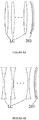
- Figures 4A and 4B are structural diagrams showing principle of temperature compensation for the LC cells according to an embodiment of the present disclosure, wherein Figure 4A shows a case that the temperature increases, and Figure 4B shows a case that the temperature decreases.
- the mirror 203 bends little along the long-side direction, which cause a curvature much less than its curvature along the short-side direction (the X-axis direction in Figure 1 ).
- the LC cells LC become concave in the X-axis direction, which are equivalent to a plurality of concave lenses being added into the optical path.
- the strip elements 204 bend the mirror 203 to have a certain curvature along its short-side direction and become a convex mirror.
- the mirror 203 bends little along the long-side direction, which causes a curvature much less than its curvature along the short-side direction (the X-axis direction in Figure 1 ).
- Figures 5A and 5B are schematic optical path diagrams showing principle of the temperature compensation according to an embodiment of the present disclosure, wherein Figure 5A shows a case where the temperature increases, and Figure 5B shows a case where the temperature decreases.
- the incident beams A and B are focused by the focusing device 105, pass through the LC cell LC, and are reflected by the mirror 203, getting back along paths B and A, respectively (as shown by dashed lines).
- the LC cell LC becomes convex, which is equivalent to a convex lens being added into the optical path (there may be two or more convex lenses corresponding to two or more LC cells, although only one is shown in Figure 5A ), so that the focal length for the incident beams A and B becomes shorter, and the beams reflected by the mirror 203 deviate outward from the original reflection paths, as shown by the solid lines.
- the mirror 203 is a concave mirror, the reflected beams may be deflected inward so as to be closer to or in consistence with the original reflection paths, thereby compensating for deformation of the LC cell due to the temperature increasing.
- the LC cell LC becomes concave, which is equivalent to a concave lens being added into the optical path (there may be two or more concave lenses corresponding to two or more LC cells, although only one is shown in Figure 5B ), so that the focal length for the incident beams A and B becomes longer, and the beams reflected by the mirror 203 deviate inward from the original reflection paths, as shown by the solid lines.
- the mirror 203 is a convex mirror, the reflected beams may be deflected outward so as to be closer to or in consistence with the original reflection paths, thereby compensating for deformation of the LC cell due to the temperature decreasing.
- influence of deformation of the LC cells due to the temperature change may be compensated for or cancelled out by selecting proper materials for the mirror 203 and the strip elements 204 and designing and optimizing size and arrangement of the strip elements 204, thereby improving the temperature stability of the wavelength selective switch 100.
- the curvature of the mirror 203 is also related to coefficient of thermal expansion, flexural rigidity, size, and distribution of the strip elements 204.
- the strip elements 204 may be arranged densely such that the space between two adjacent strip elements 204 is no more than half of the width of the strip element.
- the strip elements such as metal strips 204 may be distributed uniformly in the longitudinal direction as shown in Figure 3 . If the deformation characteristics of the LC cells are uneven along the longitudinal direction, distribution of the metal strips 204 may be adjusted along the longitudinal direction so as to accommodate to a local fluctuation of deformation characteristics of the LC cells.
- FIG. 6 shows a schematic diagram of a mirror 203 with metal strips 204 attached thereto according to another embodiment of the present disclosure.
- an interposer 205 may be provided between the metal strip 204 and the mirror 203.
- the interposer 205 may be, for example, a glass plate or a metal plate with one side fixed (for example, adhered) to the mirror 203 and the other side fixed (for example, adhered) to the metal strip 204.
- the interposer 205 can precisely control the portion of the metal strip 204 adhered to the mirror 203 and thus adjust the curvature of the mirror 203 imparted by the metal strip 204.
- a single strip 205 may be interposed between the mirror 203 and each of the four metal strips 204 on the right side, and the single strip 205 may have the same size as the metal strip 204.
- two small pieces of strips 205 may be interposed between the mirror 203 and each of the three metal strips 204 on the left side.
- the two small pieces 205 may be attached to both ends of the metal strip 204 and spaced apart from each other. In such a configuration, the curvature of the right part of the mirror 203 will be greater than the curvature of the left part of the mirror 203 with the same temperature change.
- the arrangement of the interposer 205 may vary as needed.
- the length of the single strip 205 may be less than the length of the metal strip 204, or the distance between the two small pieces 205 may be shortened to adjust the effective length of the metal strip 204 contributing to the curvature of the mirror 203.
- the interposer 205 may have various size and number of pieces and it may be adhered to desirable portions of the metal strips 204 so as to achieve a desirable curvature of the mirror 203. It is to be understood that in addition to the interposer 205, the coefficient of thermal expansion, flexural rigidity and the like of the metal strip 204 can also be adjusted so as to achieve a desirable curvature of the mirror 203.
- FIG. 7 is a schematic diagram of a wavelength selective switch 200 according to another embodiment of the present disclosure and it shows the optical path configuration in the wavelength spreading plane, i.e., the light dispersion plane of the grating.
- the wavelength selective switch 200 includes the I/O collimator 101, the birefringent polarizer 102, a beam expanding device 303, the reflective dispersion grating 104, the focusing device 105, and an attenuation switching device 206 provided in this order along the optical path.
- the same elements as those of the foregoing embodiments are denoted by the same reference numerals, and a repetitive description thereof will be omitted here.
- the beam expanding device 303 may include a plurality of pairs of prisms, each pair including two prisms paired to each other so that the light exiting from the prism pair is substantially parallel with the light incident onto the prism pair.
- the beam expanding device 303 may include a first pair of prisms 401 and 402, and a second pair of prisms 403 and 404. It will be understood that the beam expanding device 303 may include more than two pairs of prisms.
- each prism 401, 402, 403, and 404 may have a cross section of a right-angled triangular shape, and when light passes through the beam expanding device 303 the first time, it is incident onto the hypotenuse of each prism and exits from the right angle side of the prism with an exiting angle of about 0 degree.
- the expansion factor of each prism may depend on the incident angle of light on the hypotenuse. As shown in Figure 8 , when light is incident onto the hypotenuse of the prism with a particular incident angle ⁇ , the refraction angle may be equal to the apex angle ⁇ of the prism, so that the exiting beam may be substantially perpendicular to the right angle side of the prism, and the expansion factor of the prism may be described by a formula cos ⁇ /cos ⁇ .
- Each of the prisms 401, 402, 403, and 404 may be configured to satisfy the formula.
- the beam exiting from the beam expanding device 303 may be split by the reflective dispersion grating 104 and then enters again into at least one of the prism pairs in the beam expanding device 303, for example, the second pair of prisms 403 and 404 as shown in Figure 7 .
- the incident angle and the diffraction angle of the reflective dispersion grating 104 should be sufficiently separated from each other.
- the incident angle of the reflective grating 104 may have an optimum value so that the light re-entering into the second pair of prisms again after being reflected by the grating 104 is just separated from the light entering into the second pair of prisms the first time.
- the reflective grating 104 has an expansion factor of cos ⁇ 2/cos ⁇ 1 and a dispersion capability of m ⁇ /cos ⁇ 2 for a wavelength ⁇ .
- the expansion factor and the dispersion capability may be selected for the optical path depending on the bandwidth requirement of the optical system.
- the splitting angle thereof can be magnified by the second pair of prisms with a magnification factor equal to the expansion factor of the second pair of prisms. Therefore, with respect to the optical path shown in Figure 7 , the total beam expansion factor is equal to the product of the beam expansion factor of the first pair of prisms 401, 402 multiplied by the beam expansion factor of the grating 104, and the total dispersion capability is equal to the product of the dispersion capability of the grating 104 and the expansion factor of the second pair of prisms 403 and 404.
- the second pair of prisms 403 and 404 each may have an aperture such that the light entering into the second prism pair the first time does not overlap with the light entering into the second prism pair the second time, and neither of them goes beyond the prism pair.
- the aperture of the prism may be determined according to spot size of the expanded beam, which is equal to the spot size of the collimated input beam multiplied by the expansion factor of the optical path, and the wavelength separation angle, which is equal to the wavelength range multiplied by the dispersion capability of the optical path.
- the longer wavelength is dispersed more than the shorter wavelength is.
- the dispersion characteristic of the prism is opposite to that of the grating 104.
- the shorter wavelength is dispersed by the prism more than the longer wavelength is because the shorter wavelength has a higher refraction index for the same prism.
- the light further dispersed by the second pair of prisms 403 and 404 may be focused by the focusing device 105 onto the attenuation switching device 206.
- the attenuation switching device 206 may be a temperature compensation LC attenuation switching device 106 as described above with reference to Figures 1-6 , or it may be any of conventional attenuation switching devices, including but not limited to attenuation switching devices based on MEMS micro mirror array, attenuation switching devices based on LCOS pixel cell array, and attenuation switching devices based on LC cells. As described above, the attenuation switching device 206 may alter the propagation path of the reflected light so as to select an output port for the light.
- the grating may be implemented with a lower dispersion capability while achieving a uniform dispersion in the full band.
Landscapes
- Physics & Mathematics (AREA)
- General Physics & Mathematics (AREA)
- Optics & Photonics (AREA)
- Nonlinear Science (AREA)
- Chemical & Material Sciences (AREA)
- Crystallography & Structural Chemistry (AREA)
- Mathematical Physics (AREA)
- Spectroscopy & Molecular Physics (AREA)
- Mechanical Light Control Or Optical Switches (AREA)
Applications Claiming Priority (2)
| Application Number | Priority Date | Filing Date | Title |
|---|---|---|---|
| CN201610768927.9A CN106291822A (zh) | 2016-08-30 | 2016-08-30 | 一种波长选择开关 |
| CN201610776059.9A CN106199841B (zh) | 2016-08-30 | 2016-08-30 | 一种液晶型波长选择开关 |
Publications (2)
| Publication Number | Publication Date |
|---|---|
| EP3291000A1 true EP3291000A1 (de) | 2018-03-07 |
| EP3291000B1 EP3291000B1 (de) | 2020-12-16 |
Family
ID=57758441
Family Applications (1)
| Application Number | Title | Priority Date | Filing Date |
|---|---|---|---|
| EP16205761.6A Active EP3291000B1 (de) | 2016-08-30 | 2016-12-21 | Wellenlängenselektiver schalter |
Country Status (2)
| Country | Link |
|---|---|
| US (1) | US10175495B2 (de) |
| EP (1) | EP3291000B1 (de) |
Families Citing this family (6)
| Publication number | Priority date | Publication date | Assignee | Title |
|---|---|---|---|---|
| CN105182474B (zh) * | 2015-10-29 | 2018-02-09 | 武汉光迅科技股份有限公司 | 一种波长选择开关 |
| US10367596B1 (en) * | 2017-05-23 | 2019-07-30 | Ii-Vi Delaware, Inc. | Multiple wavelength selective switch with shared switch |
| JP7124611B2 (ja) * | 2018-09-28 | 2022-08-24 | 株式会社Jvcケンウッド | 光スイッチング素子 |
| US11153667B2 (en) * | 2019-10-18 | 2021-10-19 | Inlc Technology Co., Ltd. | Twin wavelength selective switch |
| WO2022190664A1 (ja) * | 2021-03-11 | 2022-09-15 | 株式会社ジャパンディスプレイ | 表示システム |
| US12345998B2 (en) * | 2022-06-03 | 2025-07-01 | Ii-Vi Delaware, Inc. | Tunable optical wedge for reducing crosstalk in wavelength selective switch |
Citations (4)
| Publication number | Priority date | Publication date | Assignee | Title |
|---|---|---|---|---|
| US7016594B1 (en) * | 2004-08-09 | 2006-03-21 | Lightconnect, Inc. | Heat actuated steering mount for maintaining frequency alignment in wavelength selective components for optical telecommunications |
| JP2012168285A (ja) * | 2011-02-10 | 2012-09-06 | Olympus Corp | 波長選択スイッチ |
| US20130194537A1 (en) * | 2012-01-30 | 2013-08-01 | Huawei Technologies Co., Ltd. | Method and Apparatus for Wavelength Selective Switch |
| US20150208143A1 (en) * | 2012-07-19 | 2015-07-23 | Finisar Corporation | Polarization Diverse Wavelength Selective Switch |
Family Cites Families (4)
| Publication number | Priority date | Publication date | Assignee | Title |
|---|---|---|---|---|
| US6915046B2 (en) * | 2002-01-22 | 2005-07-05 | Agere Sysems, Inc. | Optical systems comprising curved MEMs mirrors and methods for making same |
| US7254293B1 (en) * | 2003-06-30 | 2007-08-07 | Calient Networks, Inc. | Wavelength routing optical switch |
| US7239774B1 (en) * | 2004-08-13 | 2007-07-03 | Lightconnect, Inc. | Optical steering element and method |
| JP4489678B2 (ja) * | 2005-09-30 | 2010-06-23 | 富士通株式会社 | 波長選択光スイッチおよび分光機能を備えた光デバイス |
-
2016
- 2016-12-21 EP EP16205761.6A patent/EP3291000B1/de active Active
- 2016-12-22 US US15/388,986 patent/US10175495B2/en active Active
Patent Citations (4)
| Publication number | Priority date | Publication date | Assignee | Title |
|---|---|---|---|---|
| US7016594B1 (en) * | 2004-08-09 | 2006-03-21 | Lightconnect, Inc. | Heat actuated steering mount for maintaining frequency alignment in wavelength selective components for optical telecommunications |
| JP2012168285A (ja) * | 2011-02-10 | 2012-09-06 | Olympus Corp | 波長選択スイッチ |
| US20130194537A1 (en) * | 2012-01-30 | 2013-08-01 | Huawei Technologies Co., Ltd. | Method and Apparatus for Wavelength Selective Switch |
| US20150208143A1 (en) * | 2012-07-19 | 2015-07-23 | Finisar Corporation | Polarization Diverse Wavelength Selective Switch |
Non-Patent Citations (1)
| Title |
|---|
| FRACASSO B ET AL: "Design and performance of a versatile holographic liquid-crystal wavelength-selective optical switch", JOURNAL OF LIGHTWAVE TECHNOLOGY, IEEE SERVICE CENTER, NEW YORK, NY, US, vol. 21, no. 10, 1 October 2003 (2003-10-01), pages 2405 - 2411, XP011102208, ISSN: 0733-8724, DOI: 10.1109/JLT.2003.815512 * |
Also Published As
| Publication number | Publication date |
|---|---|
| US10175495B2 (en) | 2019-01-08 |
| EP3291000B1 (de) | 2020-12-16 |
| US20180059431A1 (en) | 2018-03-01 |
Similar Documents
| Publication | Publication Date | Title |
|---|---|---|
| EP3291000B1 (de) | Wellenlängenselektiver schalter | |
| US11366253B2 (en) | Diffractive waveplate lenses and applications | |
| US6810169B2 (en) | Wavelength switch with independent channel equalization | |
| US7499608B1 (en) | Apparatus and method for optical switching with liquid crystals and birefringent wedges | |
| EP3304154B1 (de) | Optische kopplung mit verwendung von polarisationsstrahlverdränger | |
| US9380361B2 (en) | Wavelength selective switch and wavelength selection method | |
| US6175448B1 (en) | Optical circulators using beam angle turners | |
| US20030021526A1 (en) | Dynamic dispersion compensator | |
| US7440650B2 (en) | Planar lightwave circuit based wavelength selective switch | |
| US9046657B2 (en) | Systems and methods for reducing off-axis optical aberrations in wavelength dispersed devices | |
| EP2605051B1 (de) | Optische Verarbeitungsvorrichtung mit Verwendung einer digitalen Mikrospiegelvorrichtung (DMD) und mit verringertem wellenlängenabhängigem Verlust | |
| US6577445B1 (en) | Composite birefringent crystal and filter | |
| US20020085252A1 (en) | Interleaver filters employing non-birefringent elements | |
| CN103091787A (zh) | 可调光衰减器及可调光衰减波分复用器 | |
| US20020122251A1 (en) | Wavelength selective switch and variable optical attenuator | |
| US20170023741A1 (en) | Wavelength-selecting optical switch device | |
| CN101718938B (zh) | 色散控制模块和波长阻隔器 | |
| US20110228374A1 (en) | Optical signal processing device | |
| US7565040B2 (en) | Optical device using variable polarization element | |
| CN117031794A (zh) | 一种动态信道均衡滤波器及光纤通信系统 | |
| JP5839586B2 (ja) | 光信号処理装置 | |
| CN121173389A (zh) | 一种抑制lcos wss带外弱光的装置及方法 | |
| JP4814147B2 (ja) | 光信号処理装置 | |
| WO2018165031A1 (en) | Wavelength shift invariable prism and grating system | |
| JP2009192791A (ja) | 液晶レンズ |
Legal Events
| Date | Code | Title | Description |
|---|---|---|---|
| PUAI | Public reference made under article 153(3) epc to a published international application that has entered the european phase |
Free format text: ORIGINAL CODE: 0009012 |
|
| STAA | Information on the status of an ep patent application or granted ep patent |
Free format text: STATUS: THE APPLICATION HAS BEEN PUBLISHED |
|
| AK | Designated contracting states |
Kind code of ref document: A1 Designated state(s): AL AT BE BG CH CY CZ DE DK EE ES FI FR GB GR HR HU IE IS IT LI LT LU LV MC MK MT NL NO PL PT RO RS SE SI SK SM TR |
|
| AX | Request for extension of the european patent |
Extension state: BA ME |
|
| STAA | Information on the status of an ep patent application or granted ep patent |
Free format text: STATUS: REQUEST FOR EXAMINATION WAS MADE |
|
| 17P | Request for examination filed |
Effective date: 20180410 |
|
| RBV | Designated contracting states (corrected) |
Designated state(s): AL AT BE BG CH CY CZ DE DK EE ES FI FR GB GR HR HU IE IS IT LI LT LU LV MC MK MT NL NO PL PT RO RS SE SI SK SM TR |
|
| GRAJ | Information related to disapproval of communication of intention to grant by the applicant or resumption of examination proceedings by the epo deleted |
Free format text: ORIGINAL CODE: EPIDOSDIGR1 |
|
| STAA | Information on the status of an ep patent application or granted ep patent |
Free format text: STATUS: GRANT OF PATENT IS INTENDED |
|
| GRAP | Despatch of communication of intention to grant a patent |
Free format text: ORIGINAL CODE: EPIDOSNIGR1 |
|
| INTG | Intention to grant announced |
Effective date: 20200612 |
|
| GRAJ | Information related to disapproval of communication of intention to grant by the applicant or resumption of examination proceedings by the epo deleted |
Free format text: ORIGINAL CODE: EPIDOSDIGR1 |
|
| STAA | Information on the status of an ep patent application or granted ep patent |
Free format text: STATUS: REQUEST FOR EXAMINATION WAS MADE |
|
| GRAS | Grant fee paid |
Free format text: ORIGINAL CODE: EPIDOSNIGR3 |
|
| INTC | Intention to grant announced (deleted) | ||
| STAA | Information on the status of an ep patent application or granted ep patent |
Free format text: STATUS: GRANT OF PATENT IS INTENDED |
|
| GRAP | Despatch of communication of intention to grant a patent |
Free format text: ORIGINAL CODE: EPIDOSNIGR1 |
|
| GRAA | (expected) grant |
Free format text: ORIGINAL CODE: 0009210 |
|
| STAA | Information on the status of an ep patent application or granted ep patent |
Free format text: STATUS: THE PATENT HAS BEEN GRANTED |
|
| INTG | Intention to grant announced |
Effective date: 20201105 |
|
| AK | Designated contracting states |
Kind code of ref document: B1 Designated state(s): AL AT BE BG CH CY CZ DE DK EE ES FI FR GB GR HR HU IE IS IT LI LT LU LV MC MK MT NL NO PL PT RO RS SE SI SK SM TR |
|
| REG | Reference to a national code |
Ref country code: GB Ref legal event code: FG4D |
|
| REG | Reference to a national code |
Ref country code: IE Ref legal event code: FG4D |
|
| REG | Reference to a national code |
Ref country code: DE Ref legal event code: R096 Ref document number: 602016049791 Country of ref document: DE |
|
| REG | Reference to a national code |
Ref country code: AT Ref legal event code: REF Ref document number: 1346137 Country of ref document: AT Kind code of ref document: T Effective date: 20210115 |
|
| PG25 | Lapsed in a contracting state [announced via postgrant information from national office to epo] |
Ref country code: NO Free format text: LAPSE BECAUSE OF FAILURE TO SUBMIT A TRANSLATION OF THE DESCRIPTION OR TO PAY THE FEE WITHIN THE PRESCRIBED TIME-LIMIT Effective date: 20210316 Ref country code: RS Free format text: LAPSE BECAUSE OF FAILURE TO SUBMIT A TRANSLATION OF THE DESCRIPTION OR TO PAY THE FEE WITHIN THE PRESCRIBED TIME-LIMIT Effective date: 20201216 Ref country code: FI Free format text: LAPSE BECAUSE OF FAILURE TO SUBMIT A TRANSLATION OF THE DESCRIPTION OR TO PAY THE FEE WITHIN THE PRESCRIBED TIME-LIMIT Effective date: 20201216 Ref country code: GR Free format text: LAPSE BECAUSE OF FAILURE TO SUBMIT A TRANSLATION OF THE DESCRIPTION OR TO PAY THE FEE WITHIN THE PRESCRIBED TIME-LIMIT Effective date: 20210317 |
|
| REG | Reference to a national code |
Ref country code: AT Ref legal event code: MK05 Ref document number: 1346137 Country of ref document: AT Kind code of ref document: T Effective date: 20201216 |
|
| REG | Reference to a national code |
Ref country code: NL Ref legal event code: MP Effective date: 20201216 |
|
| PG25 | Lapsed in a contracting state [announced via postgrant information from national office to epo] |
Ref country code: SE Free format text: LAPSE BECAUSE OF FAILURE TO SUBMIT A TRANSLATION OF THE DESCRIPTION OR TO PAY THE FEE WITHIN THE PRESCRIBED TIME-LIMIT Effective date: 20201216 Ref country code: BG Free format text: LAPSE BECAUSE OF FAILURE TO SUBMIT A TRANSLATION OF THE DESCRIPTION OR TO PAY THE FEE WITHIN THE PRESCRIBED TIME-LIMIT Effective date: 20210316 Ref country code: LV Free format text: LAPSE BECAUSE OF FAILURE TO SUBMIT A TRANSLATION OF THE DESCRIPTION OR TO PAY THE FEE WITHIN THE PRESCRIBED TIME-LIMIT Effective date: 20201216 |
|
| PG25 | Lapsed in a contracting state [announced via postgrant information from national office to epo] |
Ref country code: NL Free format text: LAPSE BECAUSE OF FAILURE TO SUBMIT A TRANSLATION OF THE DESCRIPTION OR TO PAY THE FEE WITHIN THE PRESCRIBED TIME-LIMIT Effective date: 20201216 Ref country code: HR Free format text: LAPSE BECAUSE OF FAILURE TO SUBMIT A TRANSLATION OF THE DESCRIPTION OR TO PAY THE FEE WITHIN THE PRESCRIBED TIME-LIMIT Effective date: 20201216 |
|
| REG | Reference to a national code |
Ref country code: LT Ref legal event code: MG9D |
|
| PG25 | Lapsed in a contracting state [announced via postgrant information from national office to epo] |
Ref country code: CZ Free format text: LAPSE BECAUSE OF FAILURE TO SUBMIT A TRANSLATION OF THE DESCRIPTION OR TO PAY THE FEE WITHIN THE PRESCRIBED TIME-LIMIT Effective date: 20201216 Ref country code: EE Free format text: LAPSE BECAUSE OF FAILURE TO SUBMIT A TRANSLATION OF THE DESCRIPTION OR TO PAY THE FEE WITHIN THE PRESCRIBED TIME-LIMIT Effective date: 20201216 Ref country code: SM Free format text: LAPSE BECAUSE OF FAILURE TO SUBMIT A TRANSLATION OF THE DESCRIPTION OR TO PAY THE FEE WITHIN THE PRESCRIBED TIME-LIMIT Effective date: 20201216 Ref country code: LT Free format text: LAPSE BECAUSE OF FAILURE TO SUBMIT A TRANSLATION OF THE DESCRIPTION OR TO PAY THE FEE WITHIN THE PRESCRIBED TIME-LIMIT Effective date: 20201216 Ref country code: SK Free format text: LAPSE BECAUSE OF FAILURE TO SUBMIT A TRANSLATION OF THE DESCRIPTION OR TO PAY THE FEE WITHIN THE PRESCRIBED TIME-LIMIT Effective date: 20201216 Ref country code: RO Free format text: LAPSE BECAUSE OF FAILURE TO SUBMIT A TRANSLATION OF THE DESCRIPTION OR TO PAY THE FEE WITHIN THE PRESCRIBED TIME-LIMIT Effective date: 20201216 Ref country code: PT Free format text: LAPSE BECAUSE OF FAILURE TO SUBMIT A TRANSLATION OF THE DESCRIPTION OR TO PAY THE FEE WITHIN THE PRESCRIBED TIME-LIMIT Effective date: 20210416 |
|
| REG | Reference to a national code |
Ref country code: CH Ref legal event code: PL |
|
| PG25 | Lapsed in a contracting state [announced via postgrant information from national office to epo] |
Ref country code: PL Free format text: LAPSE BECAUSE OF FAILURE TO SUBMIT A TRANSLATION OF THE DESCRIPTION OR TO PAY THE FEE WITHIN THE PRESCRIBED TIME-LIMIT Effective date: 20201216 Ref country code: AT Free format text: LAPSE BECAUSE OF FAILURE TO SUBMIT A TRANSLATION OF THE DESCRIPTION OR TO PAY THE FEE WITHIN THE PRESCRIBED TIME-LIMIT Effective date: 20201216 |
|
| REG | Reference to a national code |
Ref country code: BE Ref legal event code: MM Effective date: 20201231 |
|
| REG | Reference to a national code |
Ref country code: DE Ref legal event code: R097 Ref document number: 602016049791 Country of ref document: DE |
|
| PG25 | Lapsed in a contracting state [announced via postgrant information from national office to epo] |
Ref country code: IS Free format text: LAPSE BECAUSE OF FAILURE TO SUBMIT A TRANSLATION OF THE DESCRIPTION OR TO PAY THE FEE WITHIN THE PRESCRIBED TIME-LIMIT Effective date: 20210416 Ref country code: MC Free format text: LAPSE BECAUSE OF FAILURE TO SUBMIT A TRANSLATION OF THE DESCRIPTION OR TO PAY THE FEE WITHIN THE PRESCRIBED TIME-LIMIT Effective date: 20201216 |
|
| PLBE | No opposition filed within time limit |
Free format text: ORIGINAL CODE: 0009261 |
|
| STAA | Information on the status of an ep patent application or granted ep patent |
Free format text: STATUS: NO OPPOSITION FILED WITHIN TIME LIMIT |
|
| PG25 | Lapsed in a contracting state [announced via postgrant information from national office to epo] |
Ref country code: AL Free format text: LAPSE BECAUSE OF FAILURE TO SUBMIT A TRANSLATION OF THE DESCRIPTION OR TO PAY THE FEE WITHIN THE PRESCRIBED TIME-LIMIT Effective date: 20201216 Ref country code: IE Free format text: LAPSE BECAUSE OF NON-PAYMENT OF DUE FEES Effective date: 20201221 Ref country code: IT Free format text: LAPSE BECAUSE OF FAILURE TO SUBMIT A TRANSLATION OF THE DESCRIPTION OR TO PAY THE FEE WITHIN THE PRESCRIBED TIME-LIMIT Effective date: 20201216 Ref country code: LU Free format text: LAPSE BECAUSE OF NON-PAYMENT OF DUE FEES Effective date: 20201221 |
|
| 26N | No opposition filed |
Effective date: 20210917 |
|
| PG25 | Lapsed in a contracting state [announced via postgrant information from national office to epo] |
Ref country code: LI Free format text: LAPSE BECAUSE OF NON-PAYMENT OF DUE FEES Effective date: 20201231 Ref country code: DK Free format text: LAPSE BECAUSE OF FAILURE TO SUBMIT A TRANSLATION OF THE DESCRIPTION OR TO PAY THE FEE WITHIN THE PRESCRIBED TIME-LIMIT Effective date: 20201216 Ref country code: CH Free format text: LAPSE BECAUSE OF NON-PAYMENT OF DUE FEES Effective date: 20201231 |
|
| PG25 | Lapsed in a contracting state [announced via postgrant information from national office to epo] |
Ref country code: ES Free format text: LAPSE BECAUSE OF FAILURE TO SUBMIT A TRANSLATION OF THE DESCRIPTION OR TO PAY THE FEE WITHIN THE PRESCRIBED TIME-LIMIT Effective date: 20201216 |
|
| PG25 | Lapsed in a contracting state [announced via postgrant information from national office to epo] |
Ref country code: SI Free format text: LAPSE BECAUSE OF FAILURE TO SUBMIT A TRANSLATION OF THE DESCRIPTION OR TO PAY THE FEE WITHIN THE PRESCRIBED TIME-LIMIT Effective date: 20201216 |
|
| PG25 | Lapsed in a contracting state [announced via postgrant information from national office to epo] |
Ref country code: IS Free format text: LAPSE BECAUSE OF FAILURE TO SUBMIT A TRANSLATION OF THE DESCRIPTION OR TO PAY THE FEE WITHIN THE PRESCRIBED TIME-LIMIT Effective date: 20210416 Ref country code: TR Free format text: LAPSE BECAUSE OF FAILURE TO SUBMIT A TRANSLATION OF THE DESCRIPTION OR TO PAY THE FEE WITHIN THE PRESCRIBED TIME-LIMIT Effective date: 20201216 Ref country code: MT Free format text: LAPSE BECAUSE OF FAILURE TO SUBMIT A TRANSLATION OF THE DESCRIPTION OR TO PAY THE FEE WITHIN THE PRESCRIBED TIME-LIMIT Effective date: 20201216 Ref country code: CY Free format text: LAPSE BECAUSE OF FAILURE TO SUBMIT A TRANSLATION OF THE DESCRIPTION OR TO PAY THE FEE WITHIN THE PRESCRIBED TIME-LIMIT Effective date: 20201216 |
|
| PG25 | Lapsed in a contracting state [announced via postgrant information from national office to epo] |
Ref country code: MK Free format text: LAPSE BECAUSE OF FAILURE TO SUBMIT A TRANSLATION OF THE DESCRIPTION OR TO PAY THE FEE WITHIN THE PRESCRIBED TIME-LIMIT Effective date: 20201216 |
|
| PG25 | Lapsed in a contracting state [announced via postgrant information from national office to epo] |
Ref country code: BE Free format text: LAPSE BECAUSE OF NON-PAYMENT OF DUE FEES Effective date: 20201231 |
|
| PGFP | Annual fee paid to national office [announced via postgrant information from national office to epo] |
Ref country code: DE Payment date: 20251021 Year of fee payment: 10 |
|
| PGFP | Annual fee paid to national office [announced via postgrant information from national office to epo] |
Ref country code: GB Payment date: 20251105 Year of fee payment: 10 |
|
| PGFP | Annual fee paid to national office [announced via postgrant information from national office to epo] |
Ref country code: FR Payment date: 20251105 Year of fee payment: 10 |