EP3291127A1 - Aktive manipulationsdetektionsschaltung mit umgehungsdetektion und verfahren dafür - Google Patents
Aktive manipulationsdetektionsschaltung mit umgehungsdetektion und verfahren dafür Download PDFInfo
- Publication number
- EP3291127A1 EP3291127A1 EP17185190.0A EP17185190A EP3291127A1 EP 3291127 A1 EP3291127 A1 EP 3291127A1 EP 17185190 A EP17185190 A EP 17185190A EP 3291127 A1 EP3291127 A1 EP 3291127A1
- Authority
- EP
- European Patent Office
- Prior art keywords
- detection circuit
- tamper
- sweep
- active
- terminal
- Prior art date
- Legal status (The legal status is an assumption and is not a legal conclusion. Google has not performed a legal analysis and makes no representation as to the accuracy of the status listed.)
- Granted
Links
Images


Classifications
-
- H—ELECTRICITY
- H10—SEMICONDUCTOR DEVICES; ELECTRIC SOLID-STATE DEVICES NOT OTHERWISE PROVIDED FOR
- H10W—GENERIC PACKAGES, INTERCONNECTIONS, CONNECTORS OR OTHER CONSTRUCTIONAL DETAILS OF DEVICES COVERED BY CLASS H10
- H10W42/00—Arrangements for protection of devices
- H10W42/40—Arrangements for protection of devices protecting against tampering, e.g. unauthorised inspection or reverse engineering
- H10W42/405—Arrangements for protection of devices protecting against tampering, e.g. unauthorised inspection or reverse engineering using active circuits
-
- G—PHYSICS
- G06—COMPUTING OR CALCULATING; COUNTING
- G06F—ELECTRIC DIGITAL DATA PROCESSING
- G06F21/00—Security arrangements for protecting computers, components thereof, programs or data against unauthorised activity
- G06F21/70—Protecting specific internal or peripheral components, in which the protection of a component leads to protection of the entire computer
- G06F21/86—Secure or tamper-resistant housings
- G06F21/87—Secure or tamper-resistant housings by means of encapsulation, e.g. for integrated circuits
-
- H—ELECTRICITY
- H03—ELECTRONIC CIRCUITRY
- H03K—PULSE TECHNIQUE
- H03K19/00—Logic circuits, i.e. having at least two inputs acting on one output; Inverting circuits
- H03K19/003—Modifications for increasing the reliability for protection
-
- H—ELECTRICITY
- H03—ELECTRONIC CIRCUITRY
- H03K—PULSE TECHNIQUE
- H03K3/00—Circuits for generating electric pulses; Monostable, bistable or multistable circuits
- H03K3/02—Generators characterised by the type of circuit or by the means used for producing pulses
- H03K3/023—Generators characterised by the type of circuit or by the means used for producing pulses by the use of differential amplifiers or comparators, with internal or external positive feedback
- H03K3/0233—Bistable circuits
- H03K3/02337—Bistables with hysteresis, e.g. Schmitt trigger
-
- H—ELECTRICITY
- H03—ELECTRONIC CIRCUITRY
- H03K—PULSE TECHNIQUE
- H03K3/00—Circuits for generating electric pulses; Monostable, bistable or multistable circuits
- H03K3/84—Generating pulses having a predetermined statistical distribution of a parameter, e.g. random pulse generators
-
- H—ELECTRICITY
- H05—ELECTRIC TECHNIQUES NOT OTHERWISE PROVIDED FOR
- H05K—PRINTED CIRCUITS; CASINGS OR CONSTRUCTIONAL DETAILS OF ELECTRIC APPARATUS; MANUFACTURE OF ASSEMBLAGES OF ELECTRICAL COMPONENTS
- H05K1/00—Printed circuits
- H05K1/02—Details
- H05K1/0275—Security details, e.g. tampering prevention or detection
Definitions
- This disclosure relates generally to electronic circuits and more specifically to an active tamper detection circuit with bypass detection and method therefor.
- a tamper detection circuit is used to secure a device from unauthorized access by signaling an alert when continuity of a conductor is interrupted.
- a passive tamper detector may apply a voltage to a detection circuit and if the circuit is tampered with, a change in a current is detected.
- An active tamper detector may apply a signed detection signal to one end of a detector circuit and compare it with a signal received at the other end of the detection circuit.
- the detection circuit may include a plurality of conductors in the form a grid or mesh to from an active tamper loop over the device to be protected.
- a tamper detection circuit comprising: an active tamper detection circuit for being coupled to an active tamper loop formed over a device to be protected from tampering, during an active tamper detection mode, the active tamper detection circuit detecting when conductivity of the active tamper loop is broken; and a bypass detection circuit comprising: a voltage comparator having a first input terminal for being coupled to a first end of the active tamper loop, a second input terminal for being coupled to the second end of the active tamper loop, an output terminal, and a control terminal; and a variable hysteresis control circuit having an output terminal coupled to the control terminal of the voltage comparator, wherein during a calibration mode of the bypass detection circuit, the variable hysteresis control circuit for periodically sweeping an output voltage of the voltage comparator at a pre-selected step size, the periodic active tamper sweep is compared
- the bypass detection circuit may be powered by a battery.
- the tamper detection circuit may be implemented on an integrated circuit.
- the calibration mode sweep may be run once per second.
- the bypass detection circuit may further comprise: an accumulator having an input coupled to the output terminal of the voltage comparator, and an output terminal; and a match signature comparator having a first input terminal coupled to the output terminal of the accumulator, a second input terminal coupled to receive the stored sweep signature, and an output for providing a mismatch signal.
- the bypass detection circuit may further comprise: a first resistor having a first terminal coupled to a power supply voltage terminal, and a second terminal, the first resistor having a first resistance; and a second resistor having a first terminal coupled to the power supply voltage terminal, and a second terminal, the second resistor having a second resistance that is less than the first resistance; a selection circuit coupled to the second terminals of both the first and second resistors, and to the first input terminal of the voltage comparator, the selection circuit coupling the second resistor to the first input terminal of the voltage comparator during the calibration mode, and for coupling the first resistor to the first input terminal of the voltage comparator during the active tamper detection mode.
- the stored sweep signature may be determined during a boot-up sequence of the bypass detection circuit.
- the tamper detection circuit may further comprise a logic gate having a first input terminal coupled to an output terminal of the active tamper detection circuit, a second input terminal coupled to an output terminal of the bypass detection circuit, and an output terminal for providing a tamper signal.
- the tamper detection circuit may comprise an active tamper detection circuit for being coupled to an active tamper loop formed over a device to be protected from tampering, during an active tamper detection mode the active tamper detection circuit detecting when conductivity of the active tamper loop is broken; and a bypass detection circuit may further comprise: a voltage comparator having a first input terminal for being coupled to a first end of the active tamper loop, a second input terminal for being coupled to the second end of the active tamper loop, an output terminal, and a control terminal; and a variable hysteresis control circuit having an output terminal coupled to the control terminal of the voltage comparator, wherein during a calibration mode of the bypass detection circuit, the variable hysteresis control circuit for periodically sweeping an output voltage of the voltage comparator at a pre-selected step size, the periodic active tamper sweep is compared to a stored sweep signature, a mismatch between the stored sweep signature and the periodic
- the bypass detection circuit may further comprise: a first resistor having a first terminal coupled to a power supply voltage terminal, and a second terminal, the first resistor having a first resistance; and a second resistor having a first terminal coupled to the power supply voltage terminal, and a second terminal, the second resistor having a second resistance that is less than the first resistance; a selection circuit coupled to the second terminals of both the first and second resistors, and to the first input terminal of the voltage comparator, the selection circuit coupling the second resistor to the first input terminal of the voltage comparator during the calibration mode, and for coupling the first resistor to the first input terminal of the voltage comparator during the active tamper detection mode.
- the bypass detection circuit may further comprise: an accumulator having an input coupled to the output terminal of the voltage comparator, and an output terminal; and a match signature comparator having a first input terminal coupled to the output terminal of the accumulator, a second input terminal coupled to receive the stored sweep signature, and an output for providing a mismatch signal.
- the tamper detection circuit of may further comprise a logic gate having a first input terminal coupled to an output terminal of the active tamper detection circuit, a second input terminal coupled to an output terminal of the bypass detection circuit, and an output terminal for providing a tamper signal.
- a method of detecting attempted bypassing of an active tamper loop comprising: sweeping a comparator with a hysteresis voltage having a pre-selected step size to generate an output voltage sweep; comparing the output voltage sweep with a stored sweep signature; and detecting the attempted bypass if there is a mismatch between the output voltage sweep and the stored sweep signature.
- the stored sweep signature may be stored during a first sweep of the comparator with the hysteresis voltage.
- the sweeping the comparator with a hysteresis voltage may be performed periodically.
- Embodiments of the method may comprise running active tamper detection alternately with the method for detecting attempted bypassing of the active tamper loop.
- sweeping the comparator with the hysteresis voltage may further comprise providing a current through the active tamper loop during the sweeping.
- an active tamper detection circuit with bypass detection includes an active loop that is coupled to terminals of a bypass detector.
- the active loop may be a plurality of conductors, or traces, formed in a mesh or grid over a protected device.
- the bypass detector includes a voltage comparator with a variable hysteresis control circuit and a calibration engine.
- the bypass detector detects a change in impedance in the mesh when an attacker attempts to bypass the active loop using a wire.
- the calibration engine runs a hysteresis sweep on the voltage comparator and store a hysteresis sweep boot-up signature.
- the bypass detector runs a hysteresis sweep of the voltage comparator periodically at a predetermined interval. Each sweep generates a generated signature that is compared to the stored boot-up signature. Any signature mismatch of any part of the sweep will be signaled as an impedance mismatch, or tamper.
- the hysteresis step size is also programmable.
- the calibration engine can make small changes to the boot-up signature to allow for small voltage variations.
- the bypass detection runs on the device battery domain so that stored confidential information, such as a private key, can be erased if the main supply is removed. However, the stored signature is retained even when the power supply voltage is removed. An abrupt change in the generated signature between two back-to-back calibration sweeps can indicate a tamper event of the active mesh loop. Whereas a gradual change over time, such as for example, changes caused by process variations and temperature can be distinguished.
- a tamper detection circuit comprising: an active tamper detection circuit for being coupled to an active tamper loop formed over a device to be protected from tampering, during an active tamper detection mode, the active tamper detection circuit detecting when conductivity of the active tamper loop is broken; and a bypass detection circuit comprising: a voltage comparator having a first input terminal for being coupled to a first end of the active tamper loop, a second input terminal for being coupled to the second end of the active tamper loop, an output terminal, and a control terminal; and a variable hysteresis control circuit having an output terminal coupled to the control terminal of the voltage comparator, wherein during a calibration mode of the bypass detection circuit, the variable hysteresis control circuit for periodically sweeping an output voltage of the voltage comparator at a pre-selected step size, the periodic active tamper sweep is compared to a stored sweep signature, a mismatch between the stored
- the bypass detection circuit may be powered by a battery.
- the tamper detection circuit may be implemented on an integrated circuit.
- the calibration mode sweep may be run once per second.
- the bypass detection circuit may further comprise: an accumulator having an input coupled to the output terminal of the voltage comparator, and an output terminal; and a match signature comparator having a first input terminal coupled to the output terminal of the accumulator, a second input terminal coupled to receive the stored sweep signature, and an output for providing a mismatch signal.
- the bypass detection circuit may further comprise: a first resistor having a first terminal coupled to a power supply voltage terminal, and a second terminal, the first resistor having a first resistance; and a second resistor having a first terminal coupled to the power supply voltage terminal, and a second terminal, the second resistor having a second resistance that is less than the first resistance; a selection circuit coupled to the second terminals of both the first and second resistors, and to the first input terminal of the voltage comparator, the selection circuit coupling the second resistor to the first input terminal of the voltage comparator during the calibration mode, and for coupling the first resistor to the first input terminal of the voltage comparator during the active tamper detection mode.
- the stored sweep signature may be determined during a boot-up sequence of the bypass detection circuit.
- the tamper detection circuit may further comprise a logic gate having a first input terminal coupled to an output terminal of the active tamper detection circuit, a second input terminal coupled to an output terminal of the bypass detection circuit, and an output terminal for providing a tamper signal.
- a tamper detection circuit comprising: an active tamper detection circuit for being coupled to an active tamper loop formed over a device to be protected from tampering, during an active tamper detection mode the active tamper detection circuit detecting when conductivity of the active tamper loop is broken; and a bypass detection circuit comprising: a voltage comparator having a first input terminal for being coupled to a first end of the active tamper loop, a second input terminal for being coupled to the second end of the active tamper loop, an output terminal, and a control terminal; and a variable hysteresis control circuit having an output terminal coupled to the control terminal of the voltage comparator, wherein during a calibration mode of the bypass detection circuit, the variable hysteresis control circuit for periodically sweeping an output voltage of the voltage comparator at a pre-selected step size, the periodic active tamper sweep is compared to a stored sweep signature, a mismatch between the stored sweep signature
- the tamper detection circuit may be implemented on an integrated circuit.
- the bypass detection circuit may be powered by a battery.
- the stored sweep signature may be determined during a boot-up sequence of the bypass detection circuit.
- the bypass detection circuit may further comprise: a first resistor having a first terminal coupled to a power supply voltage terminal, and a second terminal, the first resistor having a first resistance; and a second resistor having a first terminal coupled to the power supply voltage terminal, and a second terminal, the second resistor having a second resistance that is less than the first resistance; a selection circuit coupled to the second terminals of both the first and second resistors, and to the first input terminal of the voltage comparator, the selection circuit coupling the second resistor to the first input terminal of the voltage comparator during the calibration mode, and for coupling the first resistor to the first input terminal of the voltage comparator during the active tamper detection mode.
- the bypass detection circuit may further comprise: an accumulator having an input coupled to the output terminal of the voltage comparator, and an output terminal; and a match signature comparator having a first input terminal coupled to the output terminal of the accumulator, a second input terminal coupled to receive the stored sweep signature, and an output for providing a mismatch signal.
- the tamper detection circuit may further comprise a logic gate having a first input terminal coupled to an output terminal of the active tamper detection circuit, a second input terminal coupled to an output terminal of the bypass detection circuit, and an output terminal for providing a tamper signal.
- a method of detecting attempted bypassing of an active tamper loop comprising: sweeping a comparator with a hysteresis voltage having a pre-selected step size to generate an output voltage sweep; comparing the output voltage sweep with a stored sweep signature; and detecting the attempted bypass if there is a mismatch between the output voltage sweep and the stored sweep signature.
- the stored sweep signature may be stored during a first sweep of the comparator with the hysteresis voltage. Sweeping the comparator with a hysteresis voltage may be performed periodically.
- the method may further comprise running active tamper detection alternately with the method for detecting attempted bypassing of the active tamper loop. Sweeping the comparator with the hysteresis voltage may further comprise providing a current through the active tamper loop during the sweeping.
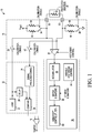
- FIG. 1 illustrates, in partial block diagram form and partial schematic diagram form, an active tamper detection circuit 10.
- Active tamper detection circuit 10 includes active tamper detector 12, bypass detector 14, OR logic gate 16, and active mesh 18.
- Tamper detector 12 includes linear feedback shift register (LFSR) 22, signal preconditioner 24, comparator 26, and delay 28.
- Bypass detector 14 includes calibration engine 30, voltage comparator 32, switches 34, 36, 38, and 40, and resistors 42, 44, 46, and 48.
- Calibration engine 30 includes variable hysteresis control 54, accumulator 56, match signature 58, and sensitivity control/filter 60.
- Active mesh 18 has a first terminal connected to a terminal 50 and a second terminal connected to a terminal 52. Active mesh 18 is illustrated as a resistor formed over a protected device 20.
- Protected device 20 may be an integrated circuit or a plurality of integrated circuits on a printed circuit board.
- Active tamper detection circuit 10 may be implemented as a portion of an integrated circuit.
- the integrated circuit may be a system-on-a-chip (SoC).
- SoC system-on-a-chip
- the integrated circuit may be a different type of integrated circuit.
- Terminals 50 and 52 are terminals of the integrated circuit having active tamper detection circuit 10. Terminal 50 and 52 are for allowing connection of both active tamper detector 12 and bypass detector 14 to the ends of active mesh 18.
- LFSR 22 has an output terminal for providing a series of bits to terminal 50 via switch 38.
- LFSR 22 may be replaced with a random number generator.
- Signal pre-conditioning block 24 has an input terminal coupled to terminal 52 switch 40, and an output terminal.
- Switches 38 and 40 are coupled to receive an enable signal labeled "CALIBRATION ENABLE" from control circuitry of calibration engine 30.
- Delay circuit 28 has an input coupled to the output of LFSR 22, and an output.
- Comparator 26 has a first input terminal coupled to output of delay 28, a second input terminal coupled to the output terminal of signal pre-conditioning block 24, and an output terminal.
- resistor 42 has a first terminal connected to a power supply voltage terminal labeled "VBAT", and a second terminal.
- Resistor 44 has a first terminal connected to power supply voltage terminal VBAT, and a second terminal.
- Switch 34 has a first terminal that is selectively coupled to either one of the second terminals of resistors 42 and 44 based on a logic state of enable signal CALIBRATION ENABLE, and a second terminal connected to terminal 50.
- Resistor 46 has a first terminal connected to terminal 52, and a second terminal.
- Resistor 48 has a first terminal connected to terminal 52, and a second terminal.
- Switch 36 has a first terminal that is selectively coupled to either one of the second terminals of resistors 46 and 48 based on the logic state of enable signal CALIBRATION ENABLE, and a second terminal connected to ground.
- Voltage comparator 32 has a first input terminal labeled plus (+) connected to terminal 50, a second input terminal labeled minus (-) connected to terminal 52, a control terminal coupled to receive a control signal labeled "HYSTERESIS CONTROL", and an output terminal.
- Calibration engine 30 has an input terminal connected to the output voltage comparator 32, and an output terminal.
- variable hysteresis control block 54 has an output for providing HYSTERESIS CONTROL.
- Accumulator 56 has an input terminal connected to the output terminal of voltage comparator 32, and an output terminal.
- Match signature block 58 has a first input terminal connected to the output terminal of accumulator 56, a second input terminal for receiving a stored comparator hysteresis signature labeled "STORED SIGNATURE", and an output terminal.
- Sensitivity control/filter 60 has an input terminal connected to the output terminal of match signature 58.
- OR logic gate 16 has a first input terminal connected to the output terminal of comparator 26, a second input terminal connected to the output terminal of calibration engine 30, and an output terminal for providing a tamper detection signal labeled "TAMPER".
- OR logic gate 16 may be a different logic gate or combination of logic gates.
- Active mesh 18 is formed as a grid or mesh of a plurality of conductive wires or traces. The wires or traces are formed on a printed circuit board (PCB) over one or more integrated circuits and other components to be protected from tampering by an attacker.
- PCB printed circuit board
- active mesh 18 is represented as a resistor over a protected device(s) 20.
- switches 42, 44, 46, and 48 are multiplexing type circuits, in another embodiment, switches 42, 44, 46, and 48 may be transmission gates.
- power supply voltage VBAT is provided by a battery and may be regulated to a predetermined voltage level. In another embodiment, the power supply voltage may be provided by a different source.
- Resistors 42 and 46 have a lower resistance value than resistors 44 and 48.
- resistors 42, and 46 are 100-ohm resistors and resistors 44 and 48 are 300-kilo ohm resistors.
- active tamper detector 12 is coupled to active mesh 18 in response to calibration enable signal CALIBRATION ENABLE being in a first predetermined logic state, closing switches 38 and 40 and causing resistors 44 and 48 to be connected to terminals 50 and 52, respectively.
- LFSR 22 provides a plurality of bits to active mesh loop 18 via switch 38 in response to a clock signal (not shown). The bits return via terminal 52 and switch 40 to the input of signal pre-conditioning block 24.
- Signal pre-conditioning block 24 provides, for example, filtering and buffering to the bits and provides the filtered and buffered bits to the second input of comparator 26. Comparator 26 compares the returning bits to the bits leaving LFSR 22.
- Delay circuit 28 provides a predetermined delay to the bits just leaving LFSR 22 to match a signal delay of returning bits from active mesh loop 18 and signal pre-conditioning block 24.
- bypass detector 14 is enabled periodically to check the integrity of active mesh loop 18.
- the active mesh loop will have an impedance.
- a wire jumper used to bypass the active mesh loop will have a different impedance.
- Bypass detector 14 uses a voltage comparator with a predetermined output signature to detect the impedance difference between the active mesh loop and the wire, even if the impedance difference is relatively small.
- a first calibration sequence is run on voltage comparator 32 and a calibration "signature" is stored. Then, each subsequent time the calibration mode sweep is run, the generated signature is compared to the stored signature, bit-by-bit.
- the stored signature is a precise indication of the voltage at which the voltage comparator output transitions from a logic high to a logic low, or from a logic low to a logic high, depending on which direction the sweep is run. Any mismatch between any of the bits and an impedance mismatch tamper signal is provided to the second input terminal of OR logic gate 16.
- calibration engine 30 provides calibration enable signal CALIBRATION ENABLE to cause switches 38 and 40 to be open, or non-conductive.
- Switch 34 connects resistor 42 to terminal 50 and switch 36 connects resistor 46 to ground.
- the lower resistance resistors 42 and 44 cause a current to flow between VBAT and ground through active mesh loop 18.
- a voltage drop across active mesh loop 18 is sensed at the plus and minus input terminals of voltage comparator 32.
- Variable hysteresis control 54 provides a multi-bit control signal HYSTERESIS CONTROL that runs a voltage sweep on voltage comparator. The use of three bits allows the output voltage of voltage comparator 32 to provide eight output bits.
- a sample hysteresis sweep is illustrated in FIG. 2 .
- the sweep step size is 1 millivolt.
- the voltage sweep step size may be variable in some embodiments.
- the first time the calibration mode has been run the output voltage values of comparator 32 are stored as stored signature STORED SIGNATURE.
- the stored signature STORED SIGNATURE may be stored in a nonvolatile memory such as a read-only memory (ROM), or in another type of one-time programmable (OTP) memory, such as electrically blown fuses or a write-once register during boot up. Then, when an active tamper detection mode is enabled, bypass detector 14 will run the voltage sweep on voltage comparator 32.
- ROM read-only memory
- OTP one-time programmable
- the generated output bits are temporarily stored in accumulator 56 and are compared to the stored signature using match signature comparator 58. Any mismatch between any of the bits will cause match signature comparator 58 to output a mismatch signal to sensitivity control/filter 60.
- the hysteresis calibration sweep is run on voltage comparator 32 every second. In another embodiment, the sweep interval may be different.
- FIG. 2 illustrates a table of example values for a hysteresis sweep using the variable hysteresis control circuit 54 of FIG. 1 .
- the first two columns show scan position and the hysteresis control signal.
- the hysteresis control signal has three bits, thus the hysteresis sweep has eight scan positions. In other embodiments, the number of control bits may be different, providing a different number of scan positions.
- a step size of one (1) millivolt (mV) is illustrated. Other step sizes can be used.
- Two columns show two possibilities for the voltage comparator 32 output that may be the stored signature STORED SIGNATURE, one is for best-case process and temperature variations (min) and the other is for worst-case process and temperature variations (max).
- FIG. 3 illustrates method 70 for running the calibration mode of the bypass detection circuit of FIG. 1 .
- Method 70 may be run by a state machine in calibration engine 30.
- N is an integer equal to the number of hysteresis control bits. In the illustrated example, N equals 3.
- step 74 if a logic zero is not caused to be output from the comparator, then the NO path is taken to step 76.
- step 79 the sweep is complete and the method continues to step 86. However, if at decision step 78, the answer was no, then the NO path is taken to step 80.
- decision step 80 it is determined if the no tamper voltage delta ( ⁇ V NT ) causes the comparator 32 output to equal one.
- step 86 if this is the first time calibration mode has been run, the stored values in accumulator 56 from steps 75 and 81 are stored in a boot-up signature register (BTSIG). If this is not first time calibration mode has been run, then the NO path is taken to decision step 90. At decision step 90, it is determined if the currently generated signature is equal to the stored signature in register BTSIG. If the answer is no, then the NO path is taken to step 92. At step 92, an impedance mismatch between the stored signature and the generated signature is detected, and a tamper signal TAMPER ( FIG. 1 ) is asserted. If at decision step 90, the generated signature is equal to the stored signature, indicating that no tamper has been detected, then the YES path is taken to step 94, where a tamper signal is not generated.
- TAMPER FIG. 1
- An active tamper detection circuit with bypass detection is provided.
- a bypass detection circuit is coupled to an active mesh loop.
- the bypass detector includes a voltage comparator with a variable hysteresis control circuit and a calibration engine.
- the bypass detector detects a change in impedance in the mesh when an attacker attempts to bypass the active loop using a wire.
- the calibration engine runs a hysteresis sweep on the voltage comparator and stores a hysteresis sweep boot-up signature.
- the bypass detector runs a hysteresis sweep of the voltage comparator periodically at a predetermined interval. Each sweep generates a generated signature that is compared to the stored boot-up signature. Any signature mismatch will be signaled as an impedance mismatch, or tamper.
- the hysteresis step size is also programmable.
- the calibration engine can make small changes to the boot-up signature to allow for small voltage variations.
- Coupled is not intended to be limited to a direct coupling or a mechanical coupling.
Landscapes
- Engineering & Computer Science (AREA)
- Computer Hardware Design (AREA)
- Theoretical Computer Science (AREA)
- Microelectronics & Electronic Packaging (AREA)
- Computer Security & Cryptography (AREA)
- Software Systems (AREA)
- Physics & Mathematics (AREA)
- General Engineering & Computer Science (AREA)
- General Physics & Mathematics (AREA)
- Semiconductor Integrated Circuits (AREA)
- Power Sources (AREA)
Applications Claiming Priority (1)
| Application Number | Priority Date | Filing Date | Title |
|---|---|---|---|
| US15/250,644 US10242955B2 (en) | 2016-08-29 | 2016-08-29 | Active tamper detection circuit with bypass detection and method therefor |
Publications (2)
| Publication Number | Publication Date |
|---|---|
| EP3291127A1 true EP3291127A1 (de) | 2018-03-07 |
| EP3291127B1 EP3291127B1 (de) | 2019-03-27 |
Family
ID=59626446
Family Applications (1)
| Application Number | Title | Priority Date | Filing Date |
|---|---|---|---|
| EP17185190.0A Not-in-force EP3291127B1 (de) | 2016-08-29 | 2017-08-07 | Aktive manipulationsdetektionsschaltung mit umgehungsdetektion und verfahren dafür |
Country Status (2)
| Country | Link |
|---|---|
| US (1) | US10242955B2 (de) |
| EP (1) | EP3291127B1 (de) |
Cited By (2)
| Publication number | Priority date | Publication date | Assignee | Title |
|---|---|---|---|---|
| CN112513654A (zh) * | 2018-08-03 | 2021-03-16 | Arm有限公司 | 集成电路中的电路变更检测 |
| WO2023244656A1 (en) * | 2022-06-14 | 2023-12-21 | Worcester Polytechnic Institute | Electronic tampering detection |
Families Citing this family (3)
| Publication number | Priority date | Publication date | Assignee | Title |
|---|---|---|---|---|
| US12299183B1 (en) * | 2020-12-31 | 2025-05-13 | Meta Platforms Technologies, Llc | Tamper detection and prevention in computer systems having one-time programmable memory |
| US20240256657A1 (en) * | 2023-01-26 | 2024-08-01 | Dell Products L.P. | System and method for intrusion detection in modular systems |
| US12663454B2 (en) * | 2023-08-13 | 2026-06-23 | Nxp B.V. | Semiconductor device having electromagnetic interference (EMI) sensors and a sensing circuit to detect EMI attacks |
Citations (2)
| Publication number | Priority date | Publication date | Assignee | Title |
|---|---|---|---|---|
| US4739276A (en) * | 1986-06-12 | 1988-04-19 | Maris Graube | Method and apparatus for digital time domain reflectometry |
| US20160211843A1 (en) * | 2015-01-16 | 2016-07-21 | Freescale Semiconductor, Inc. | Low-power open-circuit detection system |
Family Cites Families (14)
| Publication number | Priority date | Publication date | Assignee | Title |
|---|---|---|---|---|
| US4603305A (en) * | 1984-07-24 | 1986-07-29 | Cushman Electronics, Inc. | Apparatus and method for sweep oscillator calibration |
| US4647871A (en) | 1985-11-22 | 1987-03-03 | Motorola, Inc. | Adaptive impedance mismatch detector system |
| JP3233557B2 (ja) * | 1995-07-21 | 2001-11-26 | シャープ株式会社 | 半導体集積回路の閾値特性測定方法および装置 |
| US6977483B2 (en) * | 2002-08-23 | 2005-12-20 | Nissan Motor Co., Ltd. | Battery pack malfunction detection apparatus and method for detecting a disconnection at a connecting line between a given cell and a corresponding detection terminal |
| US8222917B2 (en) | 2005-11-03 | 2012-07-17 | Agate Logic, Inc. | Impedance matching and trimming apparatuses and methods using programmable resistance devices |
| US7391231B2 (en) * | 2006-06-19 | 2008-06-24 | International Business Machines Corporation | Switch selectable terminator for differential and pseudo-differential signaling |
| US8170814B2 (en) | 2007-05-15 | 2012-05-01 | At&T Intellectual Property I, L.P. | Systems and methods to determine an impedance mismatch |
| US8299825B2 (en) * | 2009-10-30 | 2012-10-30 | Apple Inc. | Electronic age detection circuit |
| GB2481836B (en) * | 2010-07-08 | 2012-06-13 | Keymat Technology Ltd | Circuit board connector with drilling tamper detection arrangement |
| US8803535B2 (en) * | 2011-06-29 | 2014-08-12 | Lsi Corporation | Impedance mismatch detection circuit |
| JP5851973B2 (ja) * | 2012-11-02 | 2016-02-03 | 日立オートモティブシステムズ株式会社 | 熱式流量計 |
| US9312880B2 (en) * | 2014-04-11 | 2016-04-12 | Entropic Communications, Llc | Method and apparatus for spectrum spreading of a pulse-density modulated waveform |
| US10333386B2 (en) * | 2014-04-25 | 2019-06-25 | Siemens Aktiengesellschaft | Method for detecting a voltage collapse |
| US11132659B2 (en) * | 2015-07-14 | 2021-09-28 | Texas Instruments Incorporated | Tamper detection |
-
2016
- 2016-08-29 US US15/250,644 patent/US10242955B2/en active Active
-
2017
- 2017-08-07 EP EP17185190.0A patent/EP3291127B1/de not_active Not-in-force
Patent Citations (2)
| Publication number | Priority date | Publication date | Assignee | Title |
|---|---|---|---|---|
| US4739276A (en) * | 1986-06-12 | 1988-04-19 | Maris Graube | Method and apparatus for digital time domain reflectometry |
| US20160211843A1 (en) * | 2015-01-16 | 2016-07-21 | Freescale Semiconductor, Inc. | Low-power open-circuit detection system |
Non-Patent Citations (2)
| Title |
|---|
| PAUL M FURTH ET AL: "On the design of low-power CMOS comparators with programmable hysteresis", CIRCUITS AND SYSTEMS (MWSCAS), 2010 53RD IEEE INTERNATIONAL MIDWEST SYMPOSIUM ON, IEEE, PISCATAWAY, NJ, USA, 1 August 2010 (2010-08-01), pages 1077 - 1080, XP031732953, ISBN: 978-1-4244-7771-5 * |
| VISHNU B KULKARNI ET AL: "Low-Voltage CMOS Comparators With Programmable Hysteresis", 10 October 2005 (2005-10-10), XP055435716, Retrieved from the Internet <URL:http://wordpress.nmsu.edu/pfurth/files/2015/06/Comparators_With_Hysteresis_Kulkarni_2005.pdf> [retrieved on 20171215] * |
Cited By (2)
| Publication number | Priority date | Publication date | Assignee | Title |
|---|---|---|---|---|
| CN112513654A (zh) * | 2018-08-03 | 2021-03-16 | Arm有限公司 | 集成电路中的电路变更检测 |
| WO2023244656A1 (en) * | 2022-06-14 | 2023-12-21 | Worcester Polytechnic Institute | Electronic tampering detection |
Also Published As
| Publication number | Publication date |
|---|---|
| US20180061780A1 (en) | 2018-03-01 |
| US10242955B2 (en) | 2019-03-26 |
| EP3291127B1 (de) | 2019-03-27 |
Similar Documents
| Publication | Publication Date | Title |
|---|---|---|
| US10242955B2 (en) | Active tamper detection circuit with bypass detection and method therefor | |
| US8380768B2 (en) | Random number generator | |
| US9419614B2 (en) | Low-power open-circuit detection system | |
| CN104272361B (zh) | 用于识别对电线路的操纵的方法和设备 | |
| CN103034818B (zh) | 用于检测和阻碍对安全系统的未授权访问和恶意攻击的系统和方法 | |
| US8896086B1 (en) | System for preventing tampering with integrated circuit | |
| CN107329074B (zh) | 芯片顶层防护层完整性检测装置 | |
| US9003559B2 (en) | Continuity check monitoring for microchip exploitation detection | |
| SE433671B (sv) | Sett och krets for provning av en integrerad kretsbricka | |
| WO2005022635A1 (ja) | 半導体装置の保護回路およびこれを備えた半導体装置 | |
| US6462558B1 (en) | Electronic circuit for monitoring voltage variation | |
| CN112513654B (zh) | 集成电路中的电路变更检测 | |
| CN112052484A (zh) | 自检电路及自检方法、安全芯片和电子卡 | |
| KR20130072086A (ko) | 퓨즈 회로 및 이의 검증 방법 | |
| CN102129593B (zh) | 适于检测通过传送能量进行的攻击的电子部件 | |
| US20150085557A1 (en) | Memory having one time programmable (otp) elements and a method of programming the memory | |
| CN103279704A (zh) | 一种芯片物理完整性检测装置与系统 | |
| US7564251B2 (en) | Method for identifying analog measuring sensors and associated assembly | |
| CN116110202B (zh) | 检测电路、方法及集成电路 | |
| CN117192216A (zh) | 一种线电阻检测电路、芯片及电子设备 | |
| CN109698997A (zh) | 用于附件和阻抗检测的系统和方法 | |
| CN212622995U (zh) | 检测电路及电子设备 | |
| KR101472696B1 (ko) | 바이너리 신호를 감지하기 위한 방법, 디바이스, 디지털 입력 장치 및 제어 유닛 | |
| CN112069554A (zh) | 外部供电电源上电结构及其方法、安全芯片和电子卡 | |
| CN104781130B (zh) | 用于揭示光信号中的错误的电路装置 |
Legal Events
| Date | Code | Title | Description |
|---|---|---|---|
| PUAI | Public reference made under article 153(3) epc to a published international application that has entered the european phase |
Free format text: ORIGINAL CODE: 0009012 |
|
| STAA | Information on the status of an ep patent application or granted ep patent |
Free format text: STATUS: THE APPLICATION HAS BEEN PUBLISHED |
|
| AK | Designated contracting states |
Kind code of ref document: A1 Designated state(s): AL AT BE BG CH CY CZ DE DK EE ES FI FR GB GR HR HU IE IS IT LI LT LU LV MC MK MT NL NO PL PT RO RS SE SI SK SM TR |
|
| AX | Request for extension of the european patent |
Extension state: BA ME |
|
| STAA | Information on the status of an ep patent application or granted ep patent |
Free format text: STATUS: REQUEST FOR EXAMINATION WAS MADE |
|
| 17P | Request for examination filed |
Effective date: 20180907 |
|
| RBV | Designated contracting states (corrected) |
Designated state(s): AL AT BE BG CH CY CZ DE DK EE ES FI FR GB GR HR HU IE IS IT LI LT LU LV MC MK MT NL NO PL PT RO RS SE SI SK SM TR |
|
| GRAP | Despatch of communication of intention to grant a patent |
Free format text: ORIGINAL CODE: EPIDOSNIGR1 |
|
| STAA | Information on the status of an ep patent application or granted ep patent |
Free format text: STATUS: GRANT OF PATENT IS INTENDED |
|
| RIC1 | Information provided on ipc code assigned before grant |
Ipc: H03K 19/003 20060101ALI20180927BHEP Ipc: H03K 3/0233 20060101ALI20180927BHEP Ipc: H03K 3/84 20060101ALI20180927BHEP Ipc: H05K 1/02 20060101ALI20180927BHEP Ipc: H01L 23/00 20060101ALI20180927BHEP Ipc: G06F 21/87 20130101AFI20180927BHEP Ipc: G01R 31/02 20060101ALI20180927BHEP |
|
| INTG | Intention to grant announced |
Effective date: 20181022 |
|
| GRAS | Grant fee paid |
Free format text: ORIGINAL CODE: EPIDOSNIGR3 |
|
| GRAA | (expected) grant |
Free format text: ORIGINAL CODE: 0009210 |
|
| STAA | Information on the status of an ep patent application or granted ep patent |
Free format text: STATUS: THE PATENT HAS BEEN GRANTED |
|
| AK | Designated contracting states |
Kind code of ref document: B1 Designated state(s): AL AT BE BG CH CY CZ DE DK EE ES FI FR GB GR HR HU IE IS IT LI LT LU LV MC MK MT NL NO PL PT RO RS SE SI SK SM TR |
|
| REG | Reference to a national code |
Ref country code: GB Ref legal event code: FG4D |
|
| REG | Reference to a national code |
Ref country code: CH Ref legal event code: EP |
|
| REG | Reference to a national code |
Ref country code: AT Ref legal event code: REF Ref document number: 1113921 Country of ref document: AT Kind code of ref document: T Effective date: 20190415 |
|
| REG | Reference to a national code |
Ref country code: IE Ref legal event code: FG4D |
|
| REG | Reference to a national code |
Ref country code: DE Ref legal event code: R096 Ref document number: 602017002932 Country of ref document: DE |
|
| PG25 | Lapsed in a contracting state [announced via postgrant information from national office to epo] |
Ref country code: SE Free format text: LAPSE BECAUSE OF FAILURE TO SUBMIT A TRANSLATION OF THE DESCRIPTION OR TO PAY THE FEE WITHIN THE PRESCRIBED TIME-LIMIT Effective date: 20190327 Ref country code: NO Free format text: LAPSE BECAUSE OF FAILURE TO SUBMIT A TRANSLATION OF THE DESCRIPTION OR TO PAY THE FEE WITHIN THE PRESCRIBED TIME-LIMIT Effective date: 20190627 Ref country code: FI Free format text: LAPSE BECAUSE OF FAILURE TO SUBMIT A TRANSLATION OF THE DESCRIPTION OR TO PAY THE FEE WITHIN THE PRESCRIBED TIME-LIMIT Effective date: 20190327 Ref country code: LT Free format text: LAPSE BECAUSE OF FAILURE TO SUBMIT A TRANSLATION OF THE DESCRIPTION OR TO PAY THE FEE WITHIN THE PRESCRIBED TIME-LIMIT Effective date: 20190327 |
|
| REG | Reference to a national code |
Ref country code: NL Ref legal event code: MP Effective date: 20190327 |
|
| PG25 | Lapsed in a contracting state [announced via postgrant information from national office to epo] |
Ref country code: NL Free format text: LAPSE BECAUSE OF FAILURE TO SUBMIT A TRANSLATION OF THE DESCRIPTION OR TO PAY THE FEE WITHIN THE PRESCRIBED TIME-LIMIT Effective date: 20190327 Ref country code: LV Free format text: LAPSE BECAUSE OF FAILURE TO SUBMIT A TRANSLATION OF THE DESCRIPTION OR TO PAY THE FEE WITHIN THE PRESCRIBED TIME-LIMIT Effective date: 20190327 Ref country code: RS Free format text: LAPSE BECAUSE OF FAILURE TO SUBMIT A TRANSLATION OF THE DESCRIPTION OR TO PAY THE FEE WITHIN THE PRESCRIBED TIME-LIMIT Effective date: 20190327 Ref country code: HR Free format text: LAPSE BECAUSE OF FAILURE TO SUBMIT A TRANSLATION OF THE DESCRIPTION OR TO PAY THE FEE WITHIN THE PRESCRIBED TIME-LIMIT Effective date: 20190327 Ref country code: GR Free format text: LAPSE BECAUSE OF FAILURE TO SUBMIT A TRANSLATION OF THE DESCRIPTION OR TO PAY THE FEE WITHIN THE PRESCRIBED TIME-LIMIT Effective date: 20190628 Ref country code: BG Free format text: LAPSE BECAUSE OF FAILURE TO SUBMIT A TRANSLATION OF THE DESCRIPTION OR TO PAY THE FEE WITHIN THE PRESCRIBED TIME-LIMIT Effective date: 20190627 |
|
| REG | Reference to a national code |
Ref country code: AT Ref legal event code: MK05 Ref document number: 1113921 Country of ref document: AT Kind code of ref document: T Effective date: 20190327 |
|
| PG25 | Lapsed in a contracting state [announced via postgrant information from national office to epo] |
Ref country code: EE Free format text: LAPSE BECAUSE OF FAILURE TO SUBMIT A TRANSLATION OF THE DESCRIPTION OR TO PAY THE FEE WITHIN THE PRESCRIBED TIME-LIMIT Effective date: 20190327 Ref country code: ES Free format text: LAPSE BECAUSE OF FAILURE TO SUBMIT A TRANSLATION OF THE DESCRIPTION OR TO PAY THE FEE WITHIN THE PRESCRIBED TIME-LIMIT Effective date: 20190327 Ref country code: RO Free format text: LAPSE BECAUSE OF FAILURE TO SUBMIT A TRANSLATION OF THE DESCRIPTION OR TO PAY THE FEE WITHIN THE PRESCRIBED TIME-LIMIT Effective date: 20190327 Ref country code: CZ Free format text: LAPSE BECAUSE OF FAILURE TO SUBMIT A TRANSLATION OF THE DESCRIPTION OR TO PAY THE FEE WITHIN THE PRESCRIBED TIME-LIMIT Effective date: 20190327 Ref country code: IT Free format text: LAPSE BECAUSE OF FAILURE TO SUBMIT A TRANSLATION OF THE DESCRIPTION OR TO PAY THE FEE WITHIN THE PRESCRIBED TIME-LIMIT Effective date: 20190327 Ref country code: PT Free format text: LAPSE BECAUSE OF FAILURE TO SUBMIT A TRANSLATION OF THE DESCRIPTION OR TO PAY THE FEE WITHIN THE PRESCRIBED TIME-LIMIT Effective date: 20190727 Ref country code: SK Free format text: LAPSE BECAUSE OF FAILURE TO SUBMIT A TRANSLATION OF THE DESCRIPTION OR TO PAY THE FEE WITHIN THE PRESCRIBED TIME-LIMIT Effective date: 20190327 Ref country code: AL Free format text: LAPSE BECAUSE OF FAILURE TO SUBMIT A TRANSLATION OF THE DESCRIPTION OR TO PAY THE FEE WITHIN THE PRESCRIBED TIME-LIMIT Effective date: 20190327 |
|
| PG25 | Lapsed in a contracting state [announced via postgrant information from national office to epo] |
Ref country code: PL Free format text: LAPSE BECAUSE OF FAILURE TO SUBMIT A TRANSLATION OF THE DESCRIPTION OR TO PAY THE FEE WITHIN THE PRESCRIBED TIME-LIMIT Effective date: 20190327 Ref country code: SM Free format text: LAPSE BECAUSE OF FAILURE TO SUBMIT A TRANSLATION OF THE DESCRIPTION OR TO PAY THE FEE WITHIN THE PRESCRIBED TIME-LIMIT Effective date: 20190327 |
|
| PG25 | Lapsed in a contracting state [announced via postgrant information from national office to epo] |
Ref country code: AT Free format text: LAPSE BECAUSE OF FAILURE TO SUBMIT A TRANSLATION OF THE DESCRIPTION OR TO PAY THE FEE WITHIN THE PRESCRIBED TIME-LIMIT Effective date: 20190327 Ref country code: IS Free format text: LAPSE BECAUSE OF FAILURE TO SUBMIT A TRANSLATION OF THE DESCRIPTION OR TO PAY THE FEE WITHIN THE PRESCRIBED TIME-LIMIT Effective date: 20190727 |
|
| REG | Reference to a national code |
Ref country code: DE Ref legal event code: R097 Ref document number: 602017002932 Country of ref document: DE |
|
| PG25 | Lapsed in a contracting state [announced via postgrant information from national office to epo] |
Ref country code: DK Free format text: LAPSE BECAUSE OF FAILURE TO SUBMIT A TRANSLATION OF THE DESCRIPTION OR TO PAY THE FEE WITHIN THE PRESCRIBED TIME-LIMIT Effective date: 20190327 |
|
| PLBE | No opposition filed within time limit |
Free format text: ORIGINAL CODE: 0009261 |
|
| STAA | Information on the status of an ep patent application or granted ep patent |
Free format text: STATUS: NO OPPOSITION FILED WITHIN TIME LIMIT |
|
| PG25 | Lapsed in a contracting state [announced via postgrant information from national office to epo] |
Ref country code: SI Free format text: LAPSE BECAUSE OF FAILURE TO SUBMIT A TRANSLATION OF THE DESCRIPTION OR TO PAY THE FEE WITHIN THE PRESCRIBED TIME-LIMIT Effective date: 20190327 |
|
| 26N | No opposition filed |
Effective date: 20200103 |
|
| PG25 | Lapsed in a contracting state [announced via postgrant information from national office to epo] |
Ref country code: TR Free format text: LAPSE BECAUSE OF FAILURE TO SUBMIT A TRANSLATION OF THE DESCRIPTION OR TO PAY THE FEE WITHIN THE PRESCRIBED TIME-LIMIT Effective date: 20190327 |
|
| PG25 | Lapsed in a contracting state [announced via postgrant information from national office to epo] |
Ref country code: MC Free format text: LAPSE BECAUSE OF FAILURE TO SUBMIT A TRANSLATION OF THE DESCRIPTION OR TO PAY THE FEE WITHIN THE PRESCRIBED TIME-LIMIT Effective date: 20190327 Ref country code: LU Free format text: LAPSE BECAUSE OF NON-PAYMENT OF DUE FEES Effective date: 20190807 |
|
| REG | Reference to a national code |
Ref country code: BE Ref legal event code: MM Effective date: 20190831 |
|
| PG25 | Lapsed in a contracting state [announced via postgrant information from national office to epo] |
Ref country code: IE Free format text: LAPSE BECAUSE OF NON-PAYMENT OF DUE FEES Effective date: 20190807 |
|
| PG25 | Lapsed in a contracting state [announced via postgrant information from national office to epo] |
Ref country code: BE Free format text: LAPSE BECAUSE OF NON-PAYMENT OF DUE FEES Effective date: 20190831 |
|
| REG | Reference to a national code |
Ref country code: CH Ref legal event code: PL |
|
| PG25 | Lapsed in a contracting state [announced via postgrant information from national office to epo] |
Ref country code: LI Free format text: LAPSE BECAUSE OF NON-PAYMENT OF DUE FEES Effective date: 20200831 Ref country code: CH Free format text: LAPSE BECAUSE OF NON-PAYMENT OF DUE FEES Effective date: 20200831 |
|
| PG25 | Lapsed in a contracting state [announced via postgrant information from national office to epo] |
Ref country code: CY Free format text: LAPSE BECAUSE OF FAILURE TO SUBMIT A TRANSLATION OF THE DESCRIPTION OR TO PAY THE FEE WITHIN THE PRESCRIBED TIME-LIMIT Effective date: 20190327 |
|
| PG25 | Lapsed in a contracting state [announced via postgrant information from national office to epo] |
Ref country code: HU Free format text: LAPSE BECAUSE OF FAILURE TO SUBMIT A TRANSLATION OF THE DESCRIPTION OR TO PAY THE FEE WITHIN THE PRESCRIBED TIME-LIMIT; INVALID AB INITIO Effective date: 20170807 Ref country code: MT Free format text: LAPSE BECAUSE OF FAILURE TO SUBMIT A TRANSLATION OF THE DESCRIPTION OR TO PAY THE FEE WITHIN THE PRESCRIBED TIME-LIMIT Effective date: 20190327 |
|
| GBPC | Gb: european patent ceased through non-payment of renewal fee |
Effective date: 20210807 |
|
| PG25 | Lapsed in a contracting state [announced via postgrant information from national office to epo] |
Ref country code: MK Free format text: LAPSE BECAUSE OF FAILURE TO SUBMIT A TRANSLATION OF THE DESCRIPTION OR TO PAY THE FEE WITHIN THE PRESCRIBED TIME-LIMIT Effective date: 20190327 |
|
| PG25 | Lapsed in a contracting state [announced via postgrant information from national office to epo] |
Ref country code: GB Free format text: LAPSE BECAUSE OF NON-PAYMENT OF DUE FEES Effective date: 20210807 |
|
| PGFP | Annual fee paid to national office [announced via postgrant information from national office to epo] |
Ref country code: DE Payment date: 20220720 Year of fee payment: 6 |
|
| PGFP | Annual fee paid to national office [announced via postgrant information from national office to epo] |
Ref country code: FR Payment date: 20220721 Year of fee payment: 6 |
|
| REG | Reference to a national code |
Ref country code: DE Ref legal event code: R119 Ref document number: 602017002932 Country of ref document: DE |
|
| PG25 | Lapsed in a contracting state [announced via postgrant information from national office to epo] |
Ref country code: FR Free format text: LAPSE BECAUSE OF NON-PAYMENT OF DUE FEES Effective date: 20230831 Ref country code: DE Free format text: LAPSE BECAUSE OF NON-PAYMENT OF DUE FEES Effective date: 20240301 |