EP3291300B1 - Afficheur électroluminescent organique - Google Patents
Afficheur électroluminescent organique Download PDFInfo
- Publication number
- EP3291300B1 EP3291300B1 EP17188502.3A EP17188502A EP3291300B1 EP 3291300 B1 EP3291300 B1 EP 3291300B1 EP 17188502 A EP17188502 A EP 17188502A EP 3291300 B1 EP3291300 B1 EP 3291300B1
- Authority
- EP
- European Patent Office
- Prior art keywords
- pixel
- sub
- green sub
- pixels
- data line
- Prior art date
- Legal status (The legal status is an assumption and is not a legal conclusion. Google has not performed a legal analysis and makes no representation as to the accuracy of the status listed.)
- Active
Links
Images


Classifications
-
- H—ELECTRICITY
- H10—SEMICONDUCTOR DEVICES; ELECTRIC SOLID-STATE DEVICES NOT OTHERWISE PROVIDED FOR
- H10K—ORGANIC ELECTRIC SOLID-STATE DEVICES
- H10K59/00—Integrated devices, or assemblies of multiple devices, comprising at least one organic light-emitting element covered by group H10K50/00
- H10K59/10—OLED displays
- H10K59/12—Active-matrix OLED [AMOLED] displays
- H10K59/123—Connection of the pixel electrodes to the thin film transistors [TFT]
-
- H—ELECTRICITY
- H10—SEMICONDUCTOR DEVICES; ELECTRIC SOLID-STATE DEVICES NOT OTHERWISE PROVIDED FOR
- H10K—ORGANIC ELECTRIC SOLID-STATE DEVICES
- H10K59/00—Integrated devices, or assemblies of multiple devices, comprising at least one organic light-emitting element covered by group H10K50/00
- H10K59/30—Devices specially adapted for multicolour light emission
- H10K59/35—Devices specially adapted for multicolour light emission comprising red-green-blue [RGB] subpixels
- H10K59/353—Devices specially adapted for multicolour light emission comprising red-green-blue [RGB] subpixels characterised by the geometrical arrangement of the RGB subpixels
-
- G—PHYSICS
- G09—EDUCATION; CRYPTOGRAPHY; DISPLAY; ADVERTISING; SEALS
- G09G—ARRANGEMENTS OR CIRCUITS FOR CONTROL OF INDICATING DEVICES USING STATIC MEANS TO PRESENT VARIABLE INFORMATION
- G09G3/00—Control arrangements or circuits, of interest only in connection with visual indicators other than cathode-ray tubes
- G09G3/20—Control arrangements or circuits, of interest only in connection with visual indicators other than cathode-ray tubes for presentation of an assembly of a number of characters, e.g. a page, by composing the assembly by combination of individual elements arranged in a matrix no fixed position being assigned to or needed to be assigned to the individual characters or partial characters
- G09G3/2007—Display of intermediate tones
- G09G3/2074—Display of intermediate tones using sub-pixels
-
- G—PHYSICS
- G09—EDUCATION; CRYPTOGRAPHY; DISPLAY; ADVERTISING; SEALS
- G09G—ARRANGEMENTS OR CIRCUITS FOR CONTROL OF INDICATING DEVICES USING STATIC MEANS TO PRESENT VARIABLE INFORMATION
- G09G3/00—Control arrangements or circuits, of interest only in connection with visual indicators other than cathode-ray tubes
- G09G3/20—Control arrangements or circuits, of interest only in connection with visual indicators other than cathode-ray tubes for presentation of an assembly of a number of characters, e.g. a page, by composing the assembly by combination of individual elements arranged in a matrix no fixed position being assigned to or needed to be assigned to the individual characters or partial characters
- G09G3/22—Control arrangements or circuits, of interest only in connection with visual indicators other than cathode-ray tubes for presentation of an assembly of a number of characters, e.g. a page, by composing the assembly by combination of individual elements arranged in a matrix no fixed position being assigned to or needed to be assigned to the individual characters or partial characters using controlled light sources
- G09G3/30—Control arrangements or circuits, of interest only in connection with visual indicators other than cathode-ray tubes for presentation of an assembly of a number of characters, e.g. a page, by composing the assembly by combination of individual elements arranged in a matrix no fixed position being assigned to or needed to be assigned to the individual characters or partial characters using controlled light sources using electroluminescent panels
- G09G3/32—Control arrangements or circuits, of interest only in connection with visual indicators other than cathode-ray tubes for presentation of an assembly of a number of characters, e.g. a page, by composing the assembly by combination of individual elements arranged in a matrix no fixed position being assigned to or needed to be assigned to the individual characters or partial characters using controlled light sources using electroluminescent panels semiconductive, e.g. using light-emitting diodes [LED]
- G09G3/3208—Control arrangements or circuits, of interest only in connection with visual indicators other than cathode-ray tubes for presentation of an assembly of a number of characters, e.g. a page, by composing the assembly by combination of individual elements arranged in a matrix no fixed position being assigned to or needed to be assigned to the individual characters or partial characters using controlled light sources using electroluminescent panels semiconductive, e.g. using light-emitting diodes [LED] organic, e.g. using organic light-emitting diodes [OLED]
- G09G3/3225—Control arrangements or circuits, of interest only in connection with visual indicators other than cathode-ray tubes for presentation of an assembly of a number of characters, e.g. a page, by composing the assembly by combination of individual elements arranged in a matrix no fixed position being assigned to or needed to be assigned to the individual characters or partial characters using controlled light sources using electroluminescent panels semiconductive, e.g. using light-emitting diodes [LED] organic, e.g. using organic light-emitting diodes [OLED] using an active matrix
- G09G3/3258—Control arrangements or circuits, of interest only in connection with visual indicators other than cathode-ray tubes for presentation of an assembly of a number of characters, e.g. a page, by composing the assembly by combination of individual elements arranged in a matrix no fixed position being assigned to or needed to be assigned to the individual characters or partial characters using controlled light sources using electroluminescent panels semiconductive, e.g. using light-emitting diodes [LED] organic, e.g. using organic light-emitting diodes [OLED] using an active matrix with pixel circuitry controlling the voltage across the light-emitting element
-
- H—ELECTRICITY
- H10—SEMICONDUCTOR DEVICES; ELECTRIC SOLID-STATE DEVICES NOT OTHERWISE PROVIDED FOR
- H10K—ORGANIC ELECTRIC SOLID-STATE DEVICES
- H10K50/00—Organic light-emitting devices
- H10K50/80—Constructional details
- H10K50/805—Electrodes
- H10K50/81—Anodes
- H10K50/814—Anodes combined with auxiliary electrodes, e.g. ITO layer combined with metal lines
-
- H—ELECTRICITY
- H10—SEMICONDUCTOR DEVICES; ELECTRIC SOLID-STATE DEVICES NOT OTHERWISE PROVIDED FOR
- H10K—ORGANIC ELECTRIC SOLID-STATE DEVICES
- H10K59/00—Integrated devices, or assemblies of multiple devices, comprising at least one organic light-emitting element covered by group H10K50/00
- H10K59/10—OLED displays
- H10K59/12—Active-matrix OLED [AMOLED] displays
- H10K59/131—Interconnections, e.g. wiring lines or terminals
-
- H—ELECTRICITY
- H10—SEMICONDUCTOR DEVICES; ELECTRIC SOLID-STATE DEVICES NOT OTHERWISE PROVIDED FOR
- H10K—ORGANIC ELECTRIC SOLID-STATE DEVICES
- H10K59/00—Integrated devices, or assemblies of multiple devices, comprising at least one organic light-emitting element covered by group H10K50/00
- H10K59/30—Devices specially adapted for multicolour light emission
- H10K59/35—Devices specially adapted for multicolour light emission comprising red-green-blue [RGB] subpixels
- H10K59/352—Devices specially adapted for multicolour light emission comprising red-green-blue [RGB] subpixels the areas of the RGB subpixels being different
-
- G—PHYSICS
- G09—EDUCATION; CRYPTOGRAPHY; DISPLAY; ADVERTISING; SEALS
- G09G—ARRANGEMENTS OR CIRCUITS FOR CONTROL OF INDICATING DEVICES USING STATIC MEANS TO PRESENT VARIABLE INFORMATION
- G09G2320/00—Control of display operating conditions
- G09G2320/06—Adjustment of display parameters
- G09G2320/0626—Adjustment of display parameters for control of overall brightness
- G09G2320/0633—Adjustment of display parameters for control of overall brightness by amplitude modulation of the brightness of the illumination source
Definitions
- the present disclosure relates to an organic light emitting display device and in more detail, to an organic light emitting display device improved in image quality.
- Examples of the display devices include a Liquid Crystal Display (LCD) device, a Plasma Display Panel (PDP) device, a Field Emission Display (FED) device, an Organic Light Emitting Display (OLED) device, and the like.
- LCD Liquid Crystal Display
- PDP Plasma Display Panel
- FED Field Emission Display
- OLED Organic Light Emitting Display
- the OLED device is a self-emitting device and has the advantages such as a high response time, a high luminous efficiency, a high brightness, and a wide viewing angle as compared with the other display devices. Therefore, the OLED device has attracted a lot of attention.
- an organic light emitting diode (OLED) applied to the OLED device is regarded as a next-generation light source which is self-luminous.
- the OLED has excellent advantages in terms of viewing angle, contrast, response speed, and power consumption as compared with liquid crystal. Furthermore, the OLED has a surface-emitting structure and thus can be easily implemented to be flexible.
- the OLED device includes at least a red sub-pixel, a green sub-pixel, and a blue sub-pixel.
- the red sub-pixel, the green sub-pixel, and the blue sub-pixel emit red, green, and blue lights, respectively.
- a full-color image may be provided through a plurality of sub-pixels.
- each of the sub-pixels includes an emission area where a red, green, or blue light is emitted and a non-emission area where a red, green, or blue light is not emitted.
- a predetermined process margin is needed between the organic emission layers. Since an organic emission layer is not disposed due to a process margin, or a bank layer is disposed to define pixels, a non-emission area is present between emission areas.
- bank layers disposed in the non-emission area are formed regularly and red sub-pixels, green sub-pixels and blue sub-pixels are disposed regularly, a color shift in which only red, green, or blue color appears in a specific linear direction may occur. In addition to the color shift, a lattice pattern can be seen.
- WO 2015/062110 A1 describes a wire layout for a subpixel arrangement. Data lines passing through the blue or red OLEDs (the largest OLED in the middle of each subpixel group) are used only for transmitting data of blue or red subpixels.
- FIG. 5 shows a staggered color patterning for a RGB top-emission display structure.
- the RGB top-emission display structure includes a top subrow and a bottom subrow.
- the top subrow includes a green OLED and a red OLED.
- the bottom subrow includes a blue OLED and a green OLED.
- the data line is used to program the green OLED and the blue OLED.
- the data line is used to program the red OLED and the green OLED.
- FIG. 2 shows a partial planar view of the OLED display.
- the pixel areas of the OLED display include a plurality of first pixels, a plurality of second pixels, and a plurality of third pixels.
- a wiring can be formed between the pixel areas on the display substrate.
- the wiring can be a data line, a scan line or a power supply line.
- US 2013/057521 A1 describes an OLED display.
- the OLED display includes a first pixel, a second pixel, and a third pixel displaying different colors and having a rectangular shape.
- the first pixel emits a first color light
- the second pixel emits a second color light
- the third pixel emits a third color light.
- the first color, the second color, and the third color may, for example, respectively be red, blue, and green.
- the present disclosure relates to an organic light emitting display device.
- green sub-pixels are disposed intersecting with adjacent data lines, respectively, which causes a difference in brightness between the adjacent green sub-pixels, so that sub-pixels can be seen as being disposed irregularly.
- the organic light emitting display device includes a blue sub-pixel and a red sub-pixel connected to data lines different from and adjacent to each other, so that the occurrence of a color shift and an artifact can be reduced.
- the organic light emitting display device includes a plurality of green sub-pixels connected to a scan line between a blue sub-pixel and a red sub-pixel, so that the sub-pixels can be disposed irregularly and an image quality can be improved.
- an organic light emitting display device includes a plurality of data lines, a plurality of scan lines disposed intersecting with the plurality of data lines, and a plurality of sub-pixels each connected to at least one of the plurality of data lines and at least one of the plurality of scan lines.
- the plurality of sub-pixels includes a red sub-pixel, a plurality of green sub-pixels, and a blue sub-pixel.
- a first green sub-pixel of the plurality of green sub-pixels is connected to a first data line of the plurality of data lines
- a second green sub-pixel of the plurality of green sub-pixels is connected to a second data line of the plurality of data lines, the second data line being adjacent to the first data line.
- At least one of the blue sub-pixel and the red sub-pixel is connected to the first data line of the plurality of data lines.
- the first green sub-pixel and the second data line overlap, and, in the first green sub-pixel a parasitic capacitance is generated between the second data line and an anode of the first green sub-pixel.
- the sub-pixels can be seen as being disposed irregularly, so that the occurrence of an artifact can be reduced.
- a green sub-pixel and a blue sub-pixel are connected to a data line and another green sub-pixel and a red sub-pixel are connected to an adjacent data line.
- the sub-pixels can be seen as being disposed irregularly, so that an artifact can be reduced.
- a blue sub-pixel, a plurality of green sub-pixels, and a red sub-pixel are disposed alternately on a scan line.
- green sub-pixels are connected to different data lines. Therefore, parasitic capacitance generated between adjacent green sub-pixels may cause a difference in brightness of light between the plurality of green sub-pixels.
- the green sub-pixels can be seen as being disposed irregularly and an image in the green sub-pixels can be compensated, so that an image quality can be improved.
- a difference in brightness may be caused by parasitic capacitance between a plurality of green sub-pixels adjacent to and connected to a data line or a scan line. Therefore, an image can be compensated due to non-uniformity in brightness, so that a color shift and an artifact caused by sub-pixels disposed regularly on a straight line can be reduced by the image compensation.
- a plurality of sub-pixels is connected to a scan line and disposed alternately in a zig-zag pattern along the scan line.
- the plurality of sub-pixels is disposed irregularly, rather than as a straight line. Therefore, a color shift in which lights of one color can be seen as if emitted along one direction and an artifact can be reduced.
- first, second, and the like are used for describing various components, these components are not confined by these terms. These terms are merely used for distinguishing one component from the other components. Therefore, a first component to be mentioned below may be a second component in a technical concept of the present disclosure.
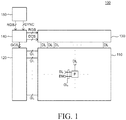
- FIG. 1 is a block diagram schematically illustrating a display device 100 according to an embodiment.
- a display device 100 includes a display panel 110, a gate driving circuit 120, a data driving circuit 130, a timing controller 140, and an image processor 150.
- the display device 100 includes the display panel 110 including a plurality of pixels P, the gate driving circuit 120 configured to supply a gate signal to each of the plurality of pixels P, the data driving circuit 130 configured to supply a data signal to each of the plurality of pixels P, and the timing controller 140 configured to control the gate driving circuit 120 and the data driving circuit 130. Further, the display device 100 includes the image processor 150 configured to receive data of an image input to the display panel 110, convert the data into a digital signal, and supply the digital signal and a control signal to the timing controller 140.
- a plurality of gate lines GL and a plurality of data lines DL are disposed to intersect with each other.
- the plurality of pixels P may be connected to at least one of the gate lines GL and the data lines DL.
- one pixel P is supplied with a gate signal from the gate driving circuit 120 through a gate line GL, a data signal from the data driving circuit 130 through a data line DL, and various powers through a power supply line.
- the gate driving circuit 120 supplies a gate signal to the gate lines GL in response to a gate control signal GCS supplied from the timing controller 140.
- each of the plurality of gate lines GL includes a scan line SL and an emission control line EM.
- the gate signal includes a scan signal and an emission control signal.
- one pixel P is supplied with the scan signal through the scan line SL and the emission control signal through the emission control line EM.
- FIG. 1 illustrates that the gate driving circuit 120 is disposed on one side of the display panel 110 as being spaced from the display panel 110, the number and position of the gate driving circuits 120 is not limited thereto. That is, the gate driving circuit 120 may be disposed on one side or both sides of the display panel 110 in a GIP (Gate In Panel) manner in some embodiments.
- GIP Gate In Panel
- the data driving circuit 130 converts image data RGB into a data voltage in response to a data control signal DCS supplied from the timing controller 140 and supplies the converted data voltage to the pixels P through the data lines DL.
- the timing controller 140 controls the timing of driving signals input to the display panel 110.
- the timing controller 140 processes the image data RGB input from the image processor 150 so as to be matched to the size and resolution of the display panel 110, and supplies the image data RGB to the data driving circuit 130.
- the timing controller 140 generates a plurality of gate control signals GCS and a plurality of data control signals DCS using synchronization signals SYNC including, for example, a dot clock DCLK, a data enable signal DE, a horizontal synchronization signal Hsync, and a vertical synchronization signal Vsync, which are timing control signals input from the image processor 150.
- the timing controller 140 supplies the generated gate control signals GCS and data control signals DCS to the gate driving circuit 120 and the data driving circuit 130, respectively, and thus controls the gate driving circuit 120 and the data driving circuit 130.
- the image processor 150 is connected to the timing controller 140 that controls the timing of driving signals input to the display panel 110.
- the image processor 150 supplies the image data RGB and the timing control signals to the timing controller 140.
- One pixel P includes a red sub-pixel, a green sub-pixel, and a blue sub-pixel. Any number of sub-pixels corresponding to each emission color may be included in one pixel P.
- Each of the sub-pixels is connected to at least one data line DL and at least one scan line SL.
- the connection relationship of a sub-pixel with respect to a data line DL and a scan line SL will be described with reference to FIGS. 2 through FIG. 5 .
- FIG. 2 is a schematic plan view of an organic light emitting display device 100 according to an embodiment.
- FIG. 1 will also be referred to for convenience in explanation.
- a plurality of sub-pixels is connected to at least one of a plurality of data lines DL and a plurality of scan lines SL.
- the plurality of sub-pixels includes a red sub-pixel SR, a green sub-pixel SG, and a blue sub-pixel SB which emit red, green, and blue lights, respectively.
- the kinds of sub-pixels are not limited thereto.
- the organic light emitting display device 100 may further include a white sub-pixel in addition to the red sub-pixel SR, the green sub-pixel SG, and the blue sub-pixel SB.
- the plurality of data lines DL includes a first data line DL1 and a second data line DL2.
- the first data line DL1 and the second data line DL2 illustrated in FIG. 2 may be any two data lines adjacent to each other among the plurality of data lines DL. That is, the first data line DL1 and the second data line DL2 are not predetermined data lines but refer to any two data lines adjacent to each other.
- each of the plurality of sub-pixels includes an anode AN and an emission area present within the anode AN.
- the anode AN includes a contact hole CT and is connected to the data line DL through the contact hole CT.
- FIG. 2 illustrates that each of the data lines DL is connected to the anode AN, at least one thin film transistor may be connected between the data line DL and the contact hole CT of the anode AN. That is, the connection between the data line DL and the contact hole CT of the anode AN illustrated in FIG. 2 is schematically illustrated to exhibit the connection relationship between each of the plurality of sub-pixels and a corresponding one of the data lines DL.
- one of a plurality of green sub-pixels SG and at least one of the blue sub-pixel SB and the red sub-pixel SR are connected to each one of the plurality of data lines DL.
- the plurality of green sub-pixels SG may include at least a first green sub-pixel SG1, a second green sub-pixel SG2, a fifth green sub-pixel SG5, and a sixth green sub-pixel SG6, among additional green sub-pixels SG.
- the first green sub-pixel SG1 and the blue sub-pixel SB are connected to the first data line DL1 among the plurality of data lines.
- the second green sub-pixel SG2 and the red sub-pixel SR are connected to the second data line DL2 adjacent to the first data line DL1 among the plurality of data lines. That is, the first green sub-pixel SG1 and the second green sub-pixel SG2 are connected to different data lines.
- the red sub-pixel SR and the blue sub-pixel SB are connected to different data lines.
- the green sub-pixels SG and the blue sub-pixels SB are connected alternately to the first data line DL1, and the green sub-pixels SG and the red sub-pixels SR are connected alternately to the second data line DL2. That is, the blue sub-pixel SB, the first green sub-pixel SG1, another blue sub-pixel SB, and another green sub-pixel SG in sequence are connected to the first data line DL1. Additionally, the fifth green sub-pixel SG5, the red sub-pixel SR, the second green sub-pixel SG2, and another red sub-pixel SR in sequence are connected to the second data line DL2.
- the first green sub-pixel SG1 and the second green sub-pixel SG2 may both overlap a vertically disposed line along an extension direction of the plurality of data lines DL.
- sub-pixels emitting lights of at least two colors are connected alternately to one data line DL. Therefore, a sub-pixel emitting light of a given color is not connected to one data line DL consecutively with another sub-pixel emitting light of the same given color. That is, the plurality of green sub-pixels SG is divided and connected to different data lines DL, and the red sub-pixel SR and the blue sub-pixel SB are also connected to different data lines DL.
- lights emitted from sub-pixels connected to each data line DL may have at least two colors with respect to the data line DL. That is, irregularity is increased as compared with a case where a data line DL is connected to sub-pixels emitting lights of only one color.
- the artifact refers to a defect which is seen as a black lattice due to a bank layer between sub-pixels when a pixel emits light.
- the blue sub-pixel SB and the first green sub-pixel SG1 connected to the first data line DL1 are disposed on one side of the first data line DL1.
- the positions of the blue sub-pixel SB and the first green sub-pixel SG1 are not limited to the illustration in FIG. 2 .
- the blue sub-pixel SB and the first green sub-pixel SG1 may be disposed alternately on one side and the other side of the first data line DL1 or may be overlapped on the first data line DL1.
- the first green sub-pixel SG1 and the second green sub-pixel SG2 may be overlapped on one data line.
- the first green sub-pixel SG1 and the second green sub-pixel SG2 may be overlapped on the second data line DL2.
- the first green sub-pixel SG1 is connected to the first data line DL1, whereas the second green sub-pixel SG2 is connected to the second data line DL2.
- parasitic capacitance between the second data line DL2 (which is not directly connected to the first green sub-pixel SG1) and the anode AN of the first green sub-pixel SG1 is generated.
- the parasitic capacitance may cause a decrease in luminous efficiency of the first green sub-pixel SG1. That is, the brightness in the first green sub-pixel SG1 may be decreased due to the parasitic capacitance.
- a brightness of a light emitted from the first green sub-pixel SG1 may be different from a brightness of a light emitted from the second green sub-pixel SG2.
- the brightness of a light emitted from the first green sub-pixel SG1 is lower than the brightness of a light emitted from the second green sub-pixel SG2.
- the plurality of green sub-pixels SG adjacent to each other along the extension direction of the data lines DL may emit lights at different brightnesses, so that a green light is seen as if emitted at a non-uniform brightness.
- the non-uniformity in brightness may compensate an image between sub-pixels. That is, when the brightness in some sub-pixels becomes different from the brightness in other sub-pixels, there may be an effect of compensating an image throughout the organic light emitting display device 100 including the plurality of sub-pixels.
- each of the red sub-pixels SR is disposed adjacent to one of the blue sub-pixels SB and thus forms a plurality of groups.
- an equal number of green sub-pixels SG among the plurality of green sub-pixels SG are disposed. That is, the blue sub-pixel SB and the red sub-pixel SR are disposed adjacent to each other as being connected to adjacent scan lines SL.
- a sub-pixel group GSBR including a blue sub-pixel SB and a red sub-pixel SR adjacent to each other along the extension direction of the plurality of scan lines SL is connected to each of the plurality of scan lines SL between green sub-pixel groups GSG including the plurality of green sub-pixels SG5 and SG6.
- the plurality of green sub-pixels SG includes the fifth green sub-pixel SG5 and the sixth green sub-pixel SG6.
- the blue sub-pixel SB, the fifth green sub-pixel SG5, the sixth green sub-pixel sG6, and the red sub-pixel SR are connected in sequence to each of the plurality of scan lines SL.
- a plurality of sub-pixels including a blue sub-pixel, a green sub-pixel, a green sub-pixel, a red sub-pixel, a blue sub-pixel, a green sub-pixel, a green sub-pixel, a red sub-pixel, a blue sub-pixel, a green sub-pixel, a green sub-pixel, a red sub-pixel, etc. may be connected in order or in sequence to one scan line SL.
- the fifth green sub-pixel SG5 and the sixth green sub-pixel SG6 are not disposed on a straight line, but disposed alternately on one side and the other side with respect to the scan line SL. Further, with respect to the scan line SL, a blue sub-pixel SB is disposed below the scan line SL, green sub-pixels are disposed above and below the scan line SL, and a red sub-pixel is disposed above the scan line SL.
- the plurality of sub-pixels including the blue sub-pixel SB, the fifth green sub-pixel SG5, the sixth green sub-pixel SG6, and the red sub-pixel SR in order is connected to the scan line SL while being disposed alternately in a zig-zag pattern (e.g., alternating above and below) with respect to the scan line SL.
- the plurality of sub-pixels is not disposed regularly on a straight line.
- a color shift in which lights of one color can be seen as if emitted along one direction and an artifact may be reduced.
- the fifth green sub-pixel SG5 and the sixth green sub-pixel SG6 are connected to different data lines DL. Further, the fifth green sub-pixel SG5 and the sixth green sub-pixel SG6 may be disposed on different data line DL. For example, the fifth green sub-pixel SG5 may be connected to the second data line DL2 while being overlapped on the same second data line DL2. Further, the sixth green sub-pixel SG6 may be connected to another second data line DL1 adjacent to the right of the second data line DL2 (on which the fifth green sub-pixel SG5 is overlapped). The sixth green sub-pixel SG6 may also be overlapped on another second data line DL2 adjacent to the right of the aforementioned first data line DL1.
- the fifth green sub-pixel SG5 is connected to the second data line DL2 and also overlapped on the same second data line DL2 to which the fifth green sub-pixel SG5 is connected.
- the sixth green sub-pixel SG6 is connected to another second data line DL2 and also overlapped on the other second data line DL2.
- parasitic capacitance between the anode AN of the sixth green sub-pixel SG6 and the second data line DL2 is generated.
- the parasitic capacitance may cause a decrease in luminous efficiency of the sixth green sub-pixel SG6. That is, the brightness in the sixth green sub-pixel SG6 may be decreased due to the parasitic capacitance.
- the brightness of a light emitted from the fifth green sub-pixel SG5 may be different from the brightness of a light emitted from the sixth green sub-pixel SG6.
- the brightness of a light emitted from the sixth green sub-pixel SG6 is lower than the brightness of a light emitted from the fifth green sub-pixel SG5.
- the plurality of green sub-pixels SG connected to different data lines DL emit green lights at different brightnesses even when the same data voltage is applied thereto.
- the green lights at different brightnesses can be seen as if different green lights are emitted. Therefore, a color shift and an artifact of the green lights may be reduced. That is, since the green sub-pixels SG adjacent to each other are connected to different data lines DL, parasitic capacitance is generated, so that there may be an effect of compensating an image between the green sub-pixels SG due to the parasitic capacitance.
- the green sub-pixels SG are connected to different data lines DL and overlapped on different data lines DL.
- parasitic capacitance is generated between adjacent green sub-pixels SG.
- the parasitic capacitance generated between the adjacent green sub-pixels SG causes a difference in brightness of light between the plurality of green sub-pixels SG. Since there is a difference in brightness of light between the plurality of green sub-pixels SG, the green sub-pixels SG can be seen as being disposed irregularly and an image in the green sub-pixels SG may be compensated, so that an image quality may be improved.
- the green sub-pixels SG vertically adjacent to each other along the data line DL are each connected to different data lines DL.
- horizontally adjacent red sub-pixels SR and blue sub-pixels SB are connected to different data lines DL.
- the red and blue sub-pixels can be seen as being disposed irregularly.
- the green sub-pixels SG are not disposed on a straight line but disposed in a zig-zag pattern with respect to the scan line SL.
- the green sub-pixels can be seen as being disposed irregularly, which may reduce an artifact or color shift caused by linear alignment of sub-pixels.
- a difference in brightness is caused by parasitic capacitance between the plurality of green sub-pixels SG adjacent to and connected to the data line DL or the scan line SL. Therefore, an image can be compensated due to non-uniformity in brightness, so that a color shift and an artifact caused by sub-pixels disposed regularly on a straight line may be reduced by the image compensation.
- an image can be compensated due to the non-uniformity in brightness caused by the green sub-pixels SG.
- the red sub-pixel SR, the green sub-pixel SG, and the blue sub-pixel SB can be seen as being disposed irregularly, which may reducean artifact and a color shift in a displayed image.
- an image quality of the organic light emitting display device 100 can be improved.
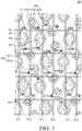
- FIG. 3 is a schematic plan view of an organic light emitting display device 300 according to an embodiment.
- the organic light emitting display device 300 illustrated in FIG. 3 is substantially the same as the organic light emitting display device 100 illustrated in FIG. 2 except for the connection relationships among sub-pixels. Therefore, a redundant explanation thereof will be omitted herein.
- green sub-pixels SG and blue sub-pixels SB or red sub-pixels SR are connected to each of the data lines DL. Additionally, the first green sub-pixel SG1 and the second green sub-pixel SG2 are connected to the same data line. For example, the first green sub-pixel SG1 and the second green sub-pixel SG2 vertically adjacent to each other are connected to the first data line DL1. Thus, a plurality of sub-pixels including the blue sub-pixel SB, the first green sub-pixel SG1, the second green sub-pixel SG2, and another blue sub-pixel SB in order or in sequence may be connected to the first data line DL1. Additionally, a plurality of sub-pixels including the fifth green sub-pixel SG5, the red sub-pixel SR, another red sub-pixel SR, and another green sub-pixel SG7 in order or in sequence may be connected to the second data line DL2.
- the first green sub-pixel SG1 and the second green sub-pixel SG2 may be disposed to overlap a same data line DL.
- the first green sub-pixel SG1 is disposed to overlap the second data line DL2.
- the plurality of green sub-pixels SG may be disposed as being connected to the first data line DL1 and the second data line DL2 in a pattern such as the second data line DL2, the first data line DL1, the first data line DL1, the second data line DL2, the second data line DL2, the first data line DL1, the first data line DL1, the second data line DL2, etc (e.g., alternating every two data lines).
- the first green sub-pixel SG1 and the second green sub-pixel SG2 may be connected to the first data line DL1 while being overlapped on the second data line DL2.
- Parasitic capacitance is generated between the second data line DL2 and the anodes AN of each of the first green sub-pixel SG1 and the second green sub-pixel SG2.
- the parasitic capacitance may cause a decrease in luminous efficiency of the first green sub-pixel SG1 and the second green sub-pixel SG2. That is, the brightness in the first green sub-pixel SG1 and the second green sub-pixel SG2 may be decreased due to the parasitic capacitance.
- the green sub-pixel SG5 connected to the second data line DL2 above the first green sub-pixel SG1 is overlapped with the second data line DL2. Therefore, the green sub-pixel SG5 is less affected by parasitic capacitance than the first green sub-pixel SG1.
- the green sub-pixel SG7 connected to the second data line DL2 below the second green sub-pixel SG2 is also overlapped with the second data line DL2. Therefore, it is less affected by parasitic capacitance than the second green sub-pixel SG2.
- the brightness of the first green sub-pixel SG1 may be different from the brightness of the fifth green sub-pixel SG5 connected to the second data line DL2 above the first green sub-pixel SG1.
- the brightness of the second green sub-pixel SG2 may be different from the brightness of the green sub-pixel SG7 connected to the second data line DL2 below the second green sub-pixel SG2.
- the brightness of the green sub-pixel SG5 connected to the second data line DL2 above the first green sub-pixel SG1 and the brightness of the green sub-pixel SG7 connected to the second data line DL2 below the second green sub-pixel SG2 are greater than the brightness of each of the first green sub-pixel SG1 and the brightness of the second green sub-pixel SG2.
- parasitic capacitance may cause a difference in brightness of adjacent green sub-pixels SG along the extension direction of the data lines DL.
- some of the green sub-pixels SG vertically adjacent to each other have a decreased brightness due to the parasitic capacitance.
- other green sub-pixels SG vertically adjacent to each other are less affected by parasitic capacitance and thus are not decreased in brightness.
- parasitic capacitance causes non-uniformity in brightness. Therefore, a green light is seen as if emitted at a non-uniform brightness throughout the organic light emitting display device 300.
- the non-uniformity in brightness may compensate an image between a plurality of sub-pixels. That is, when the brightness of some sub-pixels becomes different from the brightness of other sub-pixels, there may be an effect of compensating an image throughout the organic light emitting display device 300 including the plurality of sub-pixels.
- the blue sub-pixel SB is connected to the first data line DL1, which is also connected to the first green sub-pixel SG1 and the second green sub-pixel SG2.
- the blue sub-pixel SB is disposed above the first green sub-pixel SG1 and the second green sub-pixel SG2.
- the fifth green sub-pixel SG5 and the sixth green sub-pixel SG6 may be connected to different second data lines DL2 and disposed to overlap different second data lines DL2. That is, the fifth green sub-pixel SG5 is connected to the second data line DL2 while being overlapped on the same second data line DL2. Further, the sixth green sub-pixel SG6 is connected to another second data line DL2 adjacent to the second data line DL2 connected to the fifth green sub-pixel SG5 (with a first data line DL1 in between), and the sixth green sub-pixel SG6 overlaps the second data line DL2 to which the sixth green sub-pixel SG6 is connected.
- the fifth green sub-pixel SG5 and the sixth green sub-pixel SG6 are disposed as being overlapped on the data line DL connected to the fifth green sub-pixel SG5 and the sixth green sub-pixel SG6, respectively. Therefore, parasitic capacitance is not generated between the anodes AN of the fifth green sub-pixel SG5 and the sixth green sub-pixel SG6 and another data line DL which is not connected thereto.
- the green sub-pixels SG adjacent to each other among the green sub-pixels SG connected to a scan line SL may emit lights at the same brightens.
- FIG. 4 is a schematic plan view of an organic light emitting display device 400 according to an embodiment.
- the organic light emitting display device 400 illustrated in FIG. 4 is substantially the same as the organic light emitting display device 100 illustrated in FIG. 2 except for the connection relationships among sub-pixels. Therefore, a redundant explanation thereof will be omitted herein.
- the green sub-pixels SG may include at least the green sub-pixel SG3, green sub-pixel SG4, and green sub-pixel SG5.
- the third green sub-pixel SG3, the red sub-pixel SRI, and two blue sub-pixels SB are connected to the first data line DL1 among the plurality of data lines DL.
- a plurality of green sub-pixels SG including at least the green sub-pixel SG4 and the red sub-pixel SR2 are connected to the second data line DL2 adjacent to the first data line DL1 among the plurality of data lines DL. That is, green sub-pixels SG, red sub-pixels SR, and blue sub-pixels SB are connected to the first data line DL1, whereas another green sub-pixels SG and another red sub-pixels SR are connected to the second data line DL2.
- the blue sub-pixel SB, the green sub-pixel SG3, the red sub-pixel SRI, and the other blue sub-pixel SB are connected in order or in sequence to the first data line DL1. Further, a green sub-pixel SG, the red sub-pixel SR2, the green sub-pixel SG4, and another green sub-pixel SG are connected in order to the second data line DL2.
- sub-pixels emitting three different colors of light are connected to data line DL1 and sub-pixels emitting two colors of light are connected to its adjacent data line DL2 in an embodiment.
- the third green sub-pixel SG3 and the fourth green sub-pixel SG4 may be disposed as being overlapped on a same data line DL.
- the third green sub-pixel SG3 and the fourth green sub-pixel SG4 may be disposed to be overlapped on the second data line DL2.
- the third green sub-pixel SG3 is connected to the first data line DL1, whereas the fourth green sub-pixel SG4 is connected to the second data line DL2.
- parasitic capacitance between the second data line DL2 (which is not directly connected to the third green sub-pixel SG3) and the anode AN of the third green sub-pixel SG3 is generated.
- the parasitic capacitance may cause a decrease in luminous efficiency of the third green sub-pixel SG3. That is, the brightness in the third green sub-pixel SG3 may be decreased due to the parasitic capacitance.
- the brightness of a light emitted from the third green sub-pixel SG3 may be different from the brightness of a light emitted from the fourth green sub-pixel SG4.
- the brightness of a light emitted from the third green sub-pixel SG3 is lower than the brightness of a light emitted from the fourth green sub-pixel SG4.
- some of the green sub-pixels SG adjacent to each other along the extension direction of the data lines DL emit lights at different brightnesses, so that a green light is seen as if emitted at a non-uniform brightness.
- the non-uniformity in brightness may compensate an image between sub-pixels. That is, when the brightness in some sub-pixels becomes different from the brightness in other sub-pixels, there may be an effect of compensating an image throughout the organic light emitting display device 400 including the plurality of sub-pixels.
- the fourth green sub-pixel SG4 and the fifth green sub-pixel SG5 are connected to different data lines DL. Further, the fourth green sub-pixel SG4 and the fifth green sub-pixel SG5 may be disposed on different data lines DL. For example, the fourth green sub-pixel SG4 may be connected to the second data line DL2 while being overlapped on the same second data line DL2. Further, the fifth green sub-pixel SG5 may be connected to the first data line DL1 while being overlapped on an adjacent second data line DL2 disposed on the right side of the first data line DL1 as shown in FIG. 4 .
- parasitic capacitance is not generated between the anode AN of the green sub-pixel SG4 and the second data line DL2 to which it is connected.
- parasitic capacitance may be generated between the anode AN of the fifth green sub-pixel SG5 and the second data line DL2 adjacent to the first data line DL1 (to which the fifth green sub-pixel SG5 is connected).
- the brightness of the fifth green sub-pixel SG5 may be decreased due to the parasitic capacitance.
- the brightness of a light emitted from the fourth green sub-pixel SG4 may be different from the brightness of a light emitted from the fifth green sub-pixel SG5.
- the brightness of a light emitted from the fifth green sub-pixel SG5 is lower than the brightness of a light emitted from the fourth green sub-pixel SG4.
- the plurality of green sub-pixels SG connected to different data lines DL emit green lights at different brightnesses even when the same data voltage is applied thereto.
- the green lights at different brightnesses can be seen as if different green lights are emitted. Therefore, a color shift and an artifact of the green lights can be reduced. That is, since the green sub-pixels SG adjacent to each other are connected to different data lines DL, parasitic capacitance is generated, so that there may be an effect of compensating an image between the green sub-pixels SG due to the parasitic capacitance.
- the fourth green sub-pixel SG4 and the fifth green sub-pixel SG5 are not disposed on a straight line, but disposed alternately on one side and the other side with respect to a scan line SL. Further, with respect to the scan line SL connected to the fourth green sub-pixel SG4 and the fifth green sub-pixel SG5, green sub-pixels SG are disposed above and below the scan line SL, a blue sub-pixel SB is disposed below the scan line SL, and a red sub-pixel SR is disposed above the scan line SL. These sub-pixels are connected to the scan line SL while being disposed alternately in a zig-zag pattern with respect to the scan line SL. Accordingly, these sub-pixels are not disposed regularly on a straight line. Thus, a color shift in which lights of one color can be seen as if emitted along one direction and an artifact can be reduced.
- FIG. 5 is a schematic plan view of an organic light emitting display device 500 according to another embodiment.
- the organic light emitting display device 500 illustrated in FIG. 5 is substantially the same as the organic light emitting display device 400 illustrated in FIG. 4 except for the connection relationships among sub-pixels. Therefore, a redundant explanation thereof will be omitted herein.
- green sub-pixels SG6, two blue sub-pixels SB1 and SB2, and red sub-pixel SR1 are connected to the first data line DL1 among the plurality of data lines DL. Further, green sub-pixels SG and red sub-pixel SR2 are connected to the second data line DL2 adjacent to the right of the aforementioned first data line DL1 as shown in FIG. 5 . That is, green sub-pixels SG, red sub-pixels SR, and blue sub-pixels SB are connected to the first data line DL1, whereas another green sub-pixel SG and another red sub-pixel SR are connected to the second data line DL2.
- the blue sub-pixel SB1, the red sub-pixel SRI, the blue sub-pixel SB2, and the green sub-pixel SG6 are connected in order or in sequence to the first data line DL1. Further, a green sub-pixel SG, another green sub-pixel SG, the green sub-pixel SG5, and the red sub-pixel SR2 are connected in order or in sequence to the second data line DL2.
- sub-pixels emitting three different colors of light are connected to data line DL1 and sub-pixels emitting two colors of light are connected to an adjacent data line DL2 in an embodiment.
- the third green sub-pixel SG3 and the fourth green sub-pixel SG4 may be disposed as being overlapped on one data line DL.
- the third green sub-pixel SG3 and the fourth green sub-pixel SG4 may be disposed to be overlapped on the second data line DL2.
- the third green sub-pixel SG3 is connected to the second data line DL2 to which the third green sub-pixel SG3 overlaps, whereas the fourth green sub-pixel SG4 is connected to the first data line DL1 (adjacent to the left of the aforementioned second data line DL2).
- parasitic capacitance between the second data line DL2 (which is not directly connected to the fourth green sub-pixel SG4) and the anode AN of the fourth green sub-pixel SG4 is generated.
- the parasitic capacitance may cause a decrease in luminous efficiency of the fourth green sub-pixel SG4.
- the brightness of the fourth green sub-pixel SG4 may be decreased due to the parasitic capacitance.
- the same data voltage is applied to each of the plurality of data lines DL, the brightness of a light emitted from the third green sub-pixel SG3 is different from the brightness of a light emitted from the fourth green sub-pixel SG4.
- the brightness of a light emitted from the fourth green sub-pixel SG4 is lower than the brightness of a light emitted from the third green sub-pixel SG3.
- green sub-pixels SG adjacent to each other along the extension direction of the data lines DL emit lights at different brightnesses, so that a green light is seen as if emitted at a non-uniform brightness.
- the non-uniformity in brightness may compensate an image between sub-pixels. That is, when the brightness in some sub-pixels becomes different from the brightness in other sub-pixels, there may be an effect of compensating an image throughout the organic light emitting display device 500 including the plurality of sub-pixels.
- the fourth green sub-pixel SG4 and the fifth green sub-pixel SG5 are connected to different data lines DL. Further, the fourth green sub-pixel SG4 and the fifth green sub-pixel SG5 may be disposed on different data lines DL.
- the fifth green sub-pixel SG5 may be connected to the second data line DL2 while being overlapped on the same second data line DL2 to which the fifth green sub-pixel SG5 is connected.
- the fourth green sub-pixel SG4 may be connected to the first data line DL1 (adjacent to the right of the aforementioned second data line DL2) while being overlapped on another second data line DL2 disposed on the right side of the aforementioned first data line DL1.
- parasitic capacitance is generated between the anode AN of the fourth green sub-pixel SG4 and the second data line DL2 that the fourth green sub-pixel SG4 overlaps.
- parasitic capacitance may not be generated between the anode AN of the fifth green sub-pixel SG5 and the second data line DL2 to which the fifth green sub-pixel SG5 is connected.
- the brightness in the fourth green sub-pixel SG4 may be decreased due to the parasitic capacitance.
- the brightness of a light emitted from the fourth green sub-pixel SG4 is different from the brightness of a light emitted from the fifth green sub-pixel SG5.
- the brightness of a light emitted from the fourth green sub-pixel SG4 is lower than the brightness of a light emitted from the fifth green sub-pixel SG5.
- the plurality of green sub-pixels SG connected to different data lines DL emit green lights at different brightnesses even when the same data voltage is applied thereto.
- the green lights at different brightnesses can be seen as if different green lights are emitted. Therefore, a color shift and an artifact of the green lights can be reduced. That is, since the green sub-pixels SG adjacent to each other are connected to different data lines DL, parasitic capacitance is generated, so that there may be an effect of compensating an image between the green sub-pixels SG due to the parasitic capacitance.
- the fourth green sub-pixel SG4 and the fifth green sub-pixel SG5 are not disposed on a straight line, but disposed alternately on one side and the other side with respect to the scan line SL2. Further, with respect to the scan line SL2connected to the fourth green sub-pixel SG4 and the fifth green sub-pixel SG5, the blue sub-pixel SB2 is disposed below the scan line SL2, green sub-pixels SG are disposed above and below the scan line SL2, and the red sub-pixel SR2 is disposed below the scan line SL2. That is, the sub-pixels are connected to the scan line SL2 while being disposed alternately in a zig-zag pattern with respect to the scan line SL2. Accordingly, these sub-pixels are not disposed regularly on a straight line. Thus, a color shift in which lights of one color can be seen as if emitted along one direction and an artifact may be reduced.
Landscapes
- Engineering & Computer Science (AREA)
- Microelectronics & Electronic Packaging (AREA)
- Physics & Mathematics (AREA)
- Computer Hardware Design (AREA)
- General Physics & Mathematics (AREA)
- Theoretical Computer Science (AREA)
- Optics & Photonics (AREA)
- Electroluminescent Light Sources (AREA)
Claims (12)
- Dispositif d'affichage électroluminescent organique, comportant :une pluralité de lignes de données (DL) ;une pluralité de lignes de balayage (SL) disposées en croisant la pluralité de lignes de données (DL) ; etune pluralité de sous-pixels connectés chacun à au moins une ligne de la pluralité de lignes de données (DL) et à au moins une ligne de la pluralité de lignes de balayage (SL),dans lequel la pluralité de sous-pixels inclut un sous-pixel rouge (SR), une pluralité de sous-pixels verts (SG) et un sous-pixel bleu (SB), etun premier sous-pixel vert (SG1) de la pluralité de sous-pixels verts (SG) est connecté à une première ligne de données (DL1) de la pluralité de lignes de données (DL), un deuxième sous-pixel vert (SG2) de la pluralité de sous-pixels verts (SG) est connecté à une seconde ligne de données (DL2) de la pluralité de lignes de données (DL), la seconde ligne de données (DL2) étant adjacente à la première ligne de données (DL1), au moins un sous-pixel parmi le sous-pixel bleu (SB) et le sous-pixel rouge (SR) est connecté à la première ligne de données (DL1) de la pluralité de lignes de données (DL), caractérisé en ce que le premier sous-pixel vert (SG1) et la seconde ligne de données (DL2) se chevauchent, et, dans le premier sous-pixel vert (SG1), une capacité parasite est générée entre la seconde ligne de données (DL2) et une anode (AN) du premier sous-pixel vert (SG1).
- Dispositif d'affichage électroluminescent organique selon la revendication 1, dans lequel
le sous-pixel bleu (SB) est connecté à la première ligne de données (DL1) de la pluralité de lignes de données (DL),
le sous-pixel rouge (SR) est connecté à la seconde ligne de données (DL2), et
le premier sous-pixel vert (SG1) et le second sous-pixel vert (SG2) sont disposés verticalement le long d'une direction d'extension de la pluralité de lignes de données (DL). - Dispositif d'affichage électroluminescent organique selon la revendication 1 ou 2,
dans lequel en réponse à une même tension de données appliquée à chaque ligne de la pluralité de lignes de données (DL1, DL2), une luminosité de la lumière émise à partir du premier sous-pixel vert (SG1) est différente d'une autre luminosité de la lumière émise à partir du second sous-pixel vert (SG2). - Dispositif d'affichage électroluminescent organique selon l'une quelconque des revendications précédentes, dans lequel le sous-pixel bleu (SB) et un premier sous-ensemble de la pluralité de sous-pixels verts (SG1) sont connectés à la première ligne de données (DL1) de la pluralité de lignes de données,
le sous-pixel rouge (SR) et un second sous-ensemble de la pluralité de sous-pixels verts (SG2) sont connectés à la seconde ligne de données (DL2),
le premier sous-ensemble de la pluralité de sous-pixels verts (SG1) sont disposés verticalement le long d'une première direction d'extension de la première ligne de données (DL1), et
les sous-pixels du second sous-ensemble de la pluralité de sous-pixels verts (SG2) sont disposés verticalement le long d'une seconde direction d'extension de la seconde ligne de données (DL2). - Dispositif d'affichage électroluminescent organique selon la revendication 4, dans lequel le premier sous-ensemble de la pluralité de sous-pixels verts (SG1, SG5) sont recouverts de la seconde ligne de données (DL2), et
dans lequel les sous-pixels du second sous-ensemble de la pluralité de sous-pixels verts (SG2, SG6) recouvrent la seconde ligne de données (DL2). - Dispositif d'affichage électroluminescent organique selon la revendication 1 ou 2,
dans lequel le premier sous-pixel vert (SG1) et le second sous-pixel vert (SG2) sont chacun disposés pour recouvrir la seconde ligne de données (DL2) adjacente à la première ligne de données (DL1). - Dispositif d'affichage électroluminescent organique selon l'une quelconque des revendications précédentes, dans lequel le sous-pixel bleu (SB) et le sous-pixel rouge (SR) sont adjacents l'un à l'autre le long d'une direction d'extension de la pluralité de lignes de balayage (SL), et
dans lequel un groupe de sous-pixels (GSBR) incluant le sous-pixel bleu et le sous-pixel rouge (SB, SR) est connecté à au moins une ligne parmi la pluralité de lignes de balayage (SL) entre un sous-ensemble de la pluralité de sous-pixels verts (SG5, SG6). - Dispositif d'affichage électroluminescent organique selon l'une quelconque des revendications précédentes, comportant en outre :une pluralité de sous-pixels rouges incluant au moins le sous-pixel rouge (SR) ;une pluralité de sous-pixels bleus incluant au moins le sous-pixel bleu (SB) ;dans lequel la pluralité de sous-pixels rouges, la pluralité de sous-pixels verts et la pluralité de sous-pixels bleus sont connectés à une ligne de balayage (SL) parmi la pluralité de lignes de balayage,dans lequel chaque sous-pixel de la pluralité de sous-pixels rouges (SR) est disposé adjacent à un sous-pixel correspondant de la pluralité de sous-pixels bleus (SB) pour former une pluralité de groupes (GSBR), etdans lequel un nombre égal de sous-pixels verts (SG) de la pluralité de sous-pixels verts sont disposés entre des groupes adjacents de la pluralité de groupes.
- Dispositif d'affichage électroluminescent organique selon la revendication 8, dans lequel la pluralité de sous-pixels verts inclut un troisième sous-pixel vert (SG5) et un quatrième sous-pixel vert (SG6), le troisième sous-pixel vert (SG5) et le quatrième sous-pixel vert (SG6) étant disposés entre des groupes adjacents de la pluralité de groupes (GSBR), et
dans lequel le sous-pixel bleu (SB), le troisième sous-pixel vert (SG5), le quatrième sous-pixel vert (SG6) et le sous-pixel rouge (SR) sont connectés à la ligne de balayage (SL). - Dispositif d'affichage électroluminescent organique selon la revendication 9, dans lequel en réponse à une même tension de données appliquée à la pluralité de lignes de données (DL), une luminosité de la lumière émise à partir du troisième sous-pixel vert (SG5) est différente d'une autre luminosité de la lumière émise à partir du quatrième sous-pixel vert (SG6).
- Dispositif d'affichage électroluminescent organique selon la revendication 9 ou 10, dans lequel le troisième sous-pixel vert (SG5) et le quatrième sous-pixel vert (SG6) sont connectés à différentes lignes de données (DL).
- Dispositif d'affichage électroluminescent organique selon la revendication 9, 10 ou 11, dans lequel une autre pluralité de sous-pixels incluant un sous-pixel de la pluralité de sous-pixels bleus (SB), le troisième sous-pixel vert (SG5), le quatrième sous-pixel vert (SG6) et un sous-pixel de la pluralité des sous-pixels rouges (SR) dans cet ordre est connectée à une ligne de balayage (SL) de la pluralité de lignes de balayage et disposée en alternance selon un motif en zigzag par rapport à la ligne de balayage (SL).
Applications Claiming Priority (1)
| Application Number | Priority Date | Filing Date | Title |
|---|---|---|---|
| KR1020160112117A KR102714947B1 (ko) | 2016-08-31 | 2016-08-31 | 유기 발광 표시 장치 |
Publications (2)
| Publication Number | Publication Date |
|---|---|
| EP3291300A1 EP3291300A1 (fr) | 2018-03-07 |
| EP3291300B1 true EP3291300B1 (fr) | 2021-08-11 |
Family
ID=59846335
Family Applications (1)
| Application Number | Title | Priority Date | Filing Date |
|---|---|---|---|
| EP17188502.3A Active EP3291300B1 (fr) | 2016-08-31 | 2017-08-30 | Afficheur électroluminescent organique |
Country Status (4)
| Country | Link |
|---|---|
| US (1) | US10276822B2 (fr) |
| EP (1) | EP3291300B1 (fr) |
| KR (1) | KR102714947B1 (fr) |
| CN (1) | CN107799548B (fr) |
Families Citing this family (13)
| Publication number | Priority date | Publication date | Assignee | Title |
|---|---|---|---|---|
| KR102717107B1 (ko) * | 2018-11-30 | 2024-10-16 | 삼성디스플레이 주식회사 | 표시 패널 |
| US11100839B2 (en) * | 2019-03-22 | 2021-08-24 | Apple Inc. | Noise compensation for displays with non-rectangular borders |
| KR102922035B1 (ko) * | 2019-05-16 | 2026-02-03 | 삼성디스플레이 주식회사 | 유기발광표시장치 |
| CN112673477B (zh) * | 2019-07-31 | 2024-06-28 | 京东方科技集团股份有限公司 | 电致发光显示面板及显示装置 |
| KR20210085902A (ko) * | 2019-12-31 | 2021-07-08 | 엘지디스플레이 주식회사 | 표시장치 |
| CN119894297B (zh) * | 2020-04-26 | 2026-03-27 | 京东方科技集团股份有限公司 | 显示基板及显示装置 |
| KR20230017359A (ko) | 2020-07-01 | 2023-02-03 | 쿤산 고-비젼녹스 옵토-일렉트로닉스 씨오., 엘티디. | 픽셀 배열 구조, 디스플레이 패널 및 디스플레이 장치 |
| CN115835699A (zh) * | 2020-08-31 | 2023-03-21 | 京东方科技集团股份有限公司 | 一种显示基板和显示装置 |
| US11785821B2 (en) * | 2020-09-10 | 2023-10-10 | Chengdu Boe Optoelectronics Technology Co., Ltd. | Display substrate and related device |
| CN112562573B (zh) * | 2020-12-30 | 2024-10-11 | 厦门天马微电子有限公司 | 显示面板和显示装置 |
| CN113013202B (zh) * | 2021-02-09 | 2022-12-02 | 武汉天马微电子有限公司 | 显示面板及显示装置 |
| KR20230080759A (ko) * | 2021-11-30 | 2023-06-07 | 엘지디스플레이 주식회사 | 표시 장치 및 표시 패널 |
| CN115497993A (zh) * | 2022-08-18 | 2022-12-20 | 惠州华星光电显示有限公司 | 像素结构 |
Family Cites Families (17)
| Publication number | Priority date | Publication date | Assignee | Title |
|---|---|---|---|---|
| CN100516999C (zh) * | 2006-11-24 | 2009-07-22 | 群康科技(深圳)有限公司 | 液晶显示装置 |
| US8803417B2 (en) | 2009-12-01 | 2014-08-12 | Ignis Innovation Inc. | High resolution pixel architecture |
| KR101064430B1 (ko) * | 2010-04-13 | 2011-09-14 | 삼성모바일디스플레이주식회사 | 유기전계발광 표시장치 |
| KR101958434B1 (ko) * | 2011-09-05 | 2019-03-15 | 삼성디스플레이 주식회사 | 유기 발광 표시 장치 |
| KR102061283B1 (ko) * | 2012-09-13 | 2020-01-02 | 삼성디스플레이 주식회사 | 유기 발광 표시 장치의 화소 배열 구조 |
| KR101615332B1 (ko) * | 2012-03-06 | 2016-04-26 | 삼성디스플레이 주식회사 | 유기 발광 표시 장치의 화소 배열 구조 |
| KR101995218B1 (ko) * | 2012-03-27 | 2019-07-02 | 엘지디스플레이 주식회사 | 유기발광 표시장치 |
| KR101862793B1 (ko) | 2012-08-08 | 2018-05-31 | 삼성디스플레이 주식회사 | 화소 배열 구조 및 이를 포함한 유기전계발광 표시장치 |
| TWI481937B (zh) * | 2012-08-27 | 2015-04-21 | Au Optronics Corp | 顯示面板 |
| CN202886797U (zh) * | 2012-11-21 | 2013-04-17 | 京东方科技集团股份有限公司 | 阵列基板、显示面板及显示装置 |
| CN104871337A (zh) * | 2012-12-21 | 2015-08-26 | 伊格尼斯创新公司 | 高分辨率像素体系结构 |
| CN104885141B (zh) * | 2013-11-04 | 2018-03-16 | 深圳云英谷科技有限公司 | 显示器子像素排布及其渲染方法 |
| KR102205401B1 (ko) | 2014-01-14 | 2021-01-21 | 삼성디스플레이 주식회사 | 유기발광표시장치 |
| JP2016075868A (ja) * | 2014-10-09 | 2016-05-12 | Nltテクノロジー株式会社 | 画素アレイ及び電気光学装置並びに電気機器並びに画素レンダリング方法 |
| JP6654280B2 (ja) * | 2015-01-14 | 2020-02-26 | 天馬微電子有限公司 | 画素アレイ及び電気光学装置並びに電気機器並びに画素アレイの駆動方法 |
| CN104766564B (zh) * | 2015-04-24 | 2017-03-15 | 京东方科技集团股份有限公司 | 一种显示面板、其驱动方法及显示装置 |
| US9887247B2 (en) * | 2015-04-30 | 2018-02-06 | Novatek Microelectronics Corp. | Sub-pixel arrangement structure of organic light emitting diode display |
-
2016
- 2016-08-31 KR KR1020160112117A patent/KR102714947B1/ko active Active
-
2017
- 2017-05-27 CN CN201710389543.0A patent/CN107799548B/zh active Active
- 2017-06-13 US US15/621,974 patent/US10276822B2/en active Active
- 2017-08-30 EP EP17188502.3A patent/EP3291300B1/fr active Active
Non-Patent Citations (1)
| Title |
|---|
| None * |
Also Published As
| Publication number | Publication date |
|---|---|
| EP3291300A1 (fr) | 2018-03-07 |
| US10276822B2 (en) | 2019-04-30 |
| CN107799548B (zh) | 2021-09-21 |
| US20180062107A1 (en) | 2018-03-01 |
| CN107799548A (zh) | 2018-03-13 |
| KR20180024987A (ko) | 2018-03-08 |
| KR102714947B1 (ko) | 2024-10-07 |
Similar Documents
| Publication | Publication Date | Title |
|---|---|---|
| EP3291300B1 (fr) | Afficheur électroluminescent organique | |
| US9583034B2 (en) | Subpixel arrangement structure for display device | |
| US8354789B2 (en) | Pixel arrangement of an organic light emitting display device | |
| EP2378556B1 (fr) | Affichage électroluminescent organique | |
| KR102645930B1 (ko) | 표시장치 | |
| US20140204008A1 (en) | Pixel and sub-pixel arrangement in a display panel | |
| US9626915B2 (en) | Display device with different sub-pixel arrangements and method of driving the same | |
| KR20250133624A (ko) | 표시장치 | |
| CN114678408B (zh) | 一种显示基板和显示装置 | |
| JP2006018297A (ja) | 逆多重化装置および逆多重化装置を用いる表示装置,逆多重化装置を用いる表示装置の表示パネルとその駆動方法 | |
| KR102649645B1 (ko) | 표시 장치 | |
| KR102463347B1 (ko) | 유기발광 표시장치 | |
| KR20160018936A (ko) | 유기발광표시패널 | |
| US10910444B2 (en) | Display panel | |
| KR20180074334A (ko) | 표시장치 | |
| KR20180121292A (ko) | 발광 다이오드 디스플레이 장치 | |
| KR102891729B1 (ko) | 디스플레이 패널, 디스플레이 장치 및 디스플레이 구동 방법 | |
| KR102372062B1 (ko) | 표시 장치 | |
| US11527577B2 (en) | Array substrate and display panel having hexagonal sub-pixels | |
| KR102772536B1 (ko) | 디스플레이 장치 및 디스플레이 패널 | |
| KR102423862B1 (ko) | 유기발광 표시장치 | |
| US20250221208A1 (en) | Display panel and display device including the same | |
| US20250201779A1 (en) | Tiling display device | |
| KR102858657B1 (ko) | 발광표시패널 및 이를 이용한 발광표시장치 | |
| KR20250112992A (ko) | 픽셀 회로 및 이를 포함하는 표시 장치 |
Legal Events
| Date | Code | Title | Description |
|---|---|---|---|
| PUAI | Public reference made under article 153(3) epc to a published international application that has entered the european phase |
Free format text: ORIGINAL CODE: 0009012 |
|
| STAA | Information on the status of an ep patent application or granted ep patent |
Free format text: STATUS: REQUEST FOR EXAMINATION WAS MADE |
|
| 17P | Request for examination filed |
Effective date: 20170830 |
|
| AK | Designated contracting states |
Kind code of ref document: A1 Designated state(s): AL AT BE BG CH CY CZ DE DK EE ES FI FR GB GR HR HU IE IS IT LI LT LU LV MC MK MT NL NO PL PT RO RS SE SI SK SM TR |
|
| AX | Request for extension of the european patent |
Extension state: BA ME |
|
| RBV | Designated contracting states (corrected) |
Designated state(s): AL AT BE BG CH CY CZ DE DK EE ES FI FR GB GR HR HU IE IS IT LI LT LU LV MC MK MT NL NO PL PT RO RS SE SI SK SM TR |
|
| STAA | Information on the status of an ep patent application or granted ep patent |
Free format text: STATUS: EXAMINATION IS IN PROGRESS |
|
| 17Q | First examination report despatched |
Effective date: 20200409 |
|
| GRAP | Despatch of communication of intention to grant a patent |
Free format text: ORIGINAL CODE: EPIDOSNIGR1 |
|
| STAA | Information on the status of an ep patent application or granted ep patent |
Free format text: STATUS: GRANT OF PATENT IS INTENDED |
|
| INTG | Intention to grant announced |
Effective date: 20210305 |
|
| GRAS | Grant fee paid |
Free format text: ORIGINAL CODE: EPIDOSNIGR3 |
|
| GRAA | (expected) grant |
Free format text: ORIGINAL CODE: 0009210 |
|
| STAA | Information on the status of an ep patent application or granted ep patent |
Free format text: STATUS: THE PATENT HAS BEEN GRANTED |
|
| AK | Designated contracting states |
Kind code of ref document: B1 Designated state(s): AL AT BE BG CH CY CZ DE DK EE ES FI FR GB GR HR HU IE IS IT LI LT LU LV MC MK MT NL NO PL PT RO RS SE SI SK SM TR |
|
| REG | Reference to a national code |
Ref country code: CH Ref legal event code: EP |
|
| REG | Reference to a national code |
Ref country code: DE Ref legal event code: R096 Ref document number: 602017043724 Country of ref document: DE |
|
| REG | Reference to a national code |
Ref country code: IE Ref legal event code: FG4D Ref country code: AT Ref legal event code: REF Ref document number: 1420283 Country of ref document: AT Kind code of ref document: T Effective date: 20210915 |
|
| REG | Reference to a national code |
Ref country code: LT Ref legal event code: MG9D |
|
| REG | Reference to a national code |
Ref country code: NL Ref legal event code: MP Effective date: 20210811 |
|
| REG | Reference to a national code |
Ref country code: AT Ref legal event code: MK05 Ref document number: 1420283 Country of ref document: AT Kind code of ref document: T Effective date: 20210811 |
|
| PG25 | Lapsed in a contracting state [announced via postgrant information from national office to epo] |
Ref country code: LT Free format text: LAPSE BECAUSE OF FAILURE TO SUBMIT A TRANSLATION OF THE DESCRIPTION OR TO PAY THE FEE WITHIN THE PRESCRIBED TIME-LIMIT Effective date: 20210811 Ref country code: BG Free format text: LAPSE BECAUSE OF FAILURE TO SUBMIT A TRANSLATION OF THE DESCRIPTION OR TO PAY THE FEE WITHIN THE PRESCRIBED TIME-LIMIT Effective date: 20211111 Ref country code: AT Free format text: LAPSE BECAUSE OF FAILURE TO SUBMIT A TRANSLATION OF THE DESCRIPTION OR TO PAY THE FEE WITHIN THE PRESCRIBED TIME-LIMIT Effective date: 20210811 Ref country code: NO Free format text: LAPSE BECAUSE OF FAILURE TO SUBMIT A TRANSLATION OF THE DESCRIPTION OR TO PAY THE FEE WITHIN THE PRESCRIBED TIME-LIMIT Effective date: 20211111 Ref country code: PT Free format text: LAPSE BECAUSE OF FAILURE TO SUBMIT A TRANSLATION OF THE DESCRIPTION OR TO PAY THE FEE WITHIN THE PRESCRIBED TIME-LIMIT Effective date: 20211213 Ref country code: HR Free format text: LAPSE BECAUSE OF FAILURE TO SUBMIT A TRANSLATION OF THE DESCRIPTION OR TO PAY THE FEE WITHIN THE PRESCRIBED TIME-LIMIT Effective date: 20210811 Ref country code: FI Free format text: LAPSE BECAUSE OF FAILURE TO SUBMIT A TRANSLATION OF THE DESCRIPTION OR TO PAY THE FEE WITHIN THE PRESCRIBED TIME-LIMIT Effective date: 20210811 Ref country code: ES Free format text: LAPSE BECAUSE OF FAILURE TO SUBMIT A TRANSLATION OF THE DESCRIPTION OR TO PAY THE FEE WITHIN THE PRESCRIBED TIME-LIMIT Effective date: 20210811 Ref country code: SE Free format text: LAPSE BECAUSE OF FAILURE TO SUBMIT A TRANSLATION OF THE DESCRIPTION OR TO PAY THE FEE WITHIN THE PRESCRIBED TIME-LIMIT Effective date: 20210811 Ref country code: RS Free format text: LAPSE BECAUSE OF FAILURE TO SUBMIT A TRANSLATION OF THE DESCRIPTION OR TO PAY THE FEE WITHIN THE PRESCRIBED TIME-LIMIT Effective date: 20210811 |
|
| PG25 | Lapsed in a contracting state [announced via postgrant information from national office to epo] |
Ref country code: PL Free format text: LAPSE BECAUSE OF FAILURE TO SUBMIT A TRANSLATION OF THE DESCRIPTION OR TO PAY THE FEE WITHIN THE PRESCRIBED TIME-LIMIT Effective date: 20210811 Ref country code: LV Free format text: LAPSE BECAUSE OF FAILURE TO SUBMIT A TRANSLATION OF THE DESCRIPTION OR TO PAY THE FEE WITHIN THE PRESCRIBED TIME-LIMIT Effective date: 20210811 Ref country code: GR Free format text: LAPSE BECAUSE OF FAILURE TO SUBMIT A TRANSLATION OF THE DESCRIPTION OR TO PAY THE FEE WITHIN THE PRESCRIBED TIME-LIMIT Effective date: 20211112 |
|
| REG | Reference to a national code |
Ref country code: CH Ref legal event code: PL |
|
| PG25 | Lapsed in a contracting state [announced via postgrant information from national office to epo] |
Ref country code: NL Free format text: LAPSE BECAUSE OF FAILURE TO SUBMIT A TRANSLATION OF THE DESCRIPTION OR TO PAY THE FEE WITHIN THE PRESCRIBED TIME-LIMIT Effective date: 20210811 |
|
| REG | Reference to a national code |
Ref country code: BE Ref legal event code: MM Effective date: 20210831 |
|
| PG25 | Lapsed in a contracting state [announced via postgrant information from national office to epo] |
Ref country code: LI Free format text: LAPSE BECAUSE OF NON-PAYMENT OF DUE FEES Effective date: 20210831 Ref country code: DK Free format text: LAPSE BECAUSE OF FAILURE TO SUBMIT A TRANSLATION OF THE DESCRIPTION OR TO PAY THE FEE WITHIN THE PRESCRIBED TIME-LIMIT Effective date: 20210811 Ref country code: CH Free format text: LAPSE BECAUSE OF NON-PAYMENT OF DUE FEES Effective date: 20210831 |
|
| REG | Reference to a national code |
Ref country code: DE Ref legal event code: R097 Ref document number: 602017043724 Country of ref document: DE |
|
| PG25 | Lapsed in a contracting state [announced via postgrant information from national office to epo] |
Ref country code: SM Free format text: LAPSE BECAUSE OF FAILURE TO SUBMIT A TRANSLATION OF THE DESCRIPTION OR TO PAY THE FEE WITHIN THE PRESCRIBED TIME-LIMIT Effective date: 20210811 Ref country code: SK Free format text: LAPSE BECAUSE OF FAILURE TO SUBMIT A TRANSLATION OF THE DESCRIPTION OR TO PAY THE FEE WITHIN THE PRESCRIBED TIME-LIMIT Effective date: 20210811 Ref country code: RO Free format text: LAPSE BECAUSE OF FAILURE TO SUBMIT A TRANSLATION OF THE DESCRIPTION OR TO PAY THE FEE WITHIN THE PRESCRIBED TIME-LIMIT Effective date: 20210811 Ref country code: MC Free format text: LAPSE BECAUSE OF FAILURE TO SUBMIT A TRANSLATION OF THE DESCRIPTION OR TO PAY THE FEE WITHIN THE PRESCRIBED TIME-LIMIT Effective date: 20210811 Ref country code: LU Free format text: LAPSE BECAUSE OF NON-PAYMENT OF DUE FEES Effective date: 20210830 Ref country code: EE Free format text: LAPSE BECAUSE OF FAILURE TO SUBMIT A TRANSLATION OF THE DESCRIPTION OR TO PAY THE FEE WITHIN THE PRESCRIBED TIME-LIMIT Effective date: 20210811 Ref country code: CZ Free format text: LAPSE BECAUSE OF FAILURE TO SUBMIT A TRANSLATION OF THE DESCRIPTION OR TO PAY THE FEE WITHIN THE PRESCRIBED TIME-LIMIT Effective date: 20210811 Ref country code: AL Free format text: LAPSE BECAUSE OF FAILURE TO SUBMIT A TRANSLATION OF THE DESCRIPTION OR TO PAY THE FEE WITHIN THE PRESCRIBED TIME-LIMIT Effective date: 20210811 |
|
| PLBE | No opposition filed within time limit |
Free format text: ORIGINAL CODE: 0009261 |
|
| STAA | Information on the status of an ep patent application or granted ep patent |
Free format text: STATUS: NO OPPOSITION FILED WITHIN TIME LIMIT |
|
| 26N | No opposition filed |
Effective date: 20220512 |
|
| PG25 | Lapsed in a contracting state [announced via postgrant information from national office to epo] |
Ref country code: IT Free format text: LAPSE BECAUSE OF FAILURE TO SUBMIT A TRANSLATION OF THE DESCRIPTION OR TO PAY THE FEE WITHIN THE PRESCRIBED TIME-LIMIT Effective date: 20210811 Ref country code: IE Free format text: LAPSE BECAUSE OF NON-PAYMENT OF DUE FEES Effective date: 20210830 Ref country code: BE Free format text: LAPSE BECAUSE OF NON-PAYMENT OF DUE FEES Effective date: 20210831 |
|
| PG25 | Lapsed in a contracting state [announced via postgrant information from national office to epo] |
Ref country code: SI Free format text: LAPSE BECAUSE OF FAILURE TO SUBMIT A TRANSLATION OF THE DESCRIPTION OR TO PAY THE FEE WITHIN THE PRESCRIBED TIME-LIMIT Effective date: 20210811 |
|
| REG | Reference to a national code |
Ref country code: DE Ref legal event code: R079 Ref document number: 602017043724 Country of ref document: DE Free format text: PREVIOUS MAIN CLASS: H01L0027320000 Ipc: H10K0059000000 |
|
| PG25 | Lapsed in a contracting state [announced via postgrant information from national office to epo] |
Ref country code: HU Free format text: LAPSE BECAUSE OF FAILURE TO SUBMIT A TRANSLATION OF THE DESCRIPTION OR TO PAY THE FEE WITHIN THE PRESCRIBED TIME-LIMIT; INVALID AB INITIO Effective date: 20170830 |
|
| PG25 | Lapsed in a contracting state [announced via postgrant information from national office to epo] |
Ref country code: CY Free format text: LAPSE BECAUSE OF FAILURE TO SUBMIT A TRANSLATION OF THE DESCRIPTION OR TO PAY THE FEE WITHIN THE PRESCRIBED TIME-LIMIT Effective date: 20210811 |
|
| PG25 | Lapsed in a contracting state [announced via postgrant information from national office to epo] |
Ref country code: MK Free format text: LAPSE BECAUSE OF FAILURE TO SUBMIT A TRANSLATION OF THE DESCRIPTION OR TO PAY THE FEE WITHIN THE PRESCRIBED TIME-LIMIT Effective date: 20210811 |
|
| PG25 | Lapsed in a contracting state [announced via postgrant information from national office to epo] |
Ref country code: TR Free format text: LAPSE BECAUSE OF FAILURE TO SUBMIT A TRANSLATION OF THE DESCRIPTION OR TO PAY THE FEE WITHIN THE PRESCRIBED TIME-LIMIT Effective date: 20210811 |
|
| PG25 | Lapsed in a contracting state [announced via postgrant information from national office to epo] |
Ref country code: MT Free format text: LAPSE BECAUSE OF FAILURE TO SUBMIT A TRANSLATION OF THE DESCRIPTION OR TO PAY THE FEE WITHIN THE PRESCRIBED TIME-LIMIT Effective date: 20210811 |
|
| PGFP | Annual fee paid to national office [announced via postgrant information from national office to epo] |
Ref country code: GB Payment date: 20250624 Year of fee payment: 9 |
|
| PGFP | Annual fee paid to national office [announced via postgrant information from national office to epo] |
Ref country code: FR Payment date: 20250624 Year of fee payment: 9 |
|
| PGFP | Annual fee paid to national office [announced via postgrant information from national office to epo] |
Ref country code: DE Payment date: 20250624 Year of fee payment: 9 |