EP3291442B1 - Onduleur photovoltaique - Google Patents
Onduleur photovoltaique Download PDFInfo
- Publication number
- EP3291442B1 EP3291442B1 EP17171334.0A EP17171334A EP3291442B1 EP 3291442 B1 EP3291442 B1 EP 3291442B1 EP 17171334 A EP17171334 A EP 17171334A EP 3291442 B1 EP3291442 B1 EP 3291442B1
- Authority
- EP
- European Patent Office
- Prior art keywords
- solar cell
- cell array
- voltage
- link capacitor
- switch
- Prior art date
- Legal status (The legal status is an assumption and is not a legal conclusion. Google has not performed a legal analysis and makes no representation as to the accuracy of the status listed.)
- Active
Links
Images



Classifications
-
- H—ELECTRICITY
- H02—GENERATION; CONVERSION OR DISTRIBUTION OF ELECTRIC POWER
- H02M—APPARATUS FOR CONVERSION BETWEEN AC AND AC, BETWEEN AC AND DC, OR BETWEEN DC AND DC, AND FOR USE WITH MAINS OR SIMILAR POWER SUPPLY SYSTEMS; CONVERSION OF DC OR AC INPUT POWER INTO SURGE OUTPUT POWER; CONTROL OR REGULATION THEREOF
- H02M1/00—Details of apparatus for conversion
- H02M1/14—Arrangements for reducing ripples from DC input or output
-
- H—ELECTRICITY
- H02—GENERATION; CONVERSION OR DISTRIBUTION OF ELECTRIC POWER
- H02S—GENERATION OF ELECTRIC POWER BY CONVERSION OF INFRARED RADIATION, VISIBLE LIGHT OR ULTRAVIOLET LIGHT, e.g. USING PHOTOVOLTAIC [PV] MODULES
- H02S40/00—Components or accessories in combination with PV modules, not provided for in groups H02S10/00 - H02S30/00
- H02S40/30—Electrical components
-
- H—ELECTRICITY
- H02—GENERATION; CONVERSION OR DISTRIBUTION OF ELECTRIC POWER
- H02J—ELECTRIC POWER NETWORKS; CIRCUIT ARRANGEMENTS OR SYSTEMS FOR SUPPLYING OR DISTRIBUTING ELECTRIC POWER; SYSTEMS FOR STORING ELECTRIC ENERGY
- H02J1/00—Circuit arrangements for DC mains or DC distribution networks
- H02J1/02—Arrangements for reducing harmonics or ripples
-
- H—ELECTRICITY
- H02—GENERATION; CONVERSION OR DISTRIBUTION OF ELECTRIC POWER
- H02M—APPARATUS FOR CONVERSION BETWEEN AC AND AC, BETWEEN AC AND DC, OR BETWEEN DC AND DC, AND FOR USE WITH MAINS OR SIMILAR POWER SUPPLY SYSTEMS; CONVERSION OF DC OR AC INPUT POWER INTO SURGE OUTPUT POWER; CONTROL OR REGULATION THEREOF
- H02M7/00—Conversion of AC power input into DC power output; Conversion of DC power input into AC power output
- H02M7/42—Conversion of DC power input into AC power output without possibility of reversal
- H02M7/44—Conversion of DC power input into AC power output without possibility of reversal by static converters
- H02M7/48—Conversion of DC power input into AC power output without possibility of reversal by static converters using discharge tubes with control electrode or semiconductor devices with control electrode
- H02M7/4826—Conversion of DC power input into AC power output without possibility of reversal by static converters using discharge tubes with control electrode or semiconductor devices with control electrode operating from a resonant DC source, i.e. the DC input voltage varies periodically, e.g. resonant DC-link inverters
-
- H—ELECTRICITY
- H02—GENERATION; CONVERSION OR DISTRIBUTION OF ELECTRIC POWER
- H02S—GENERATION OF ELECTRIC POWER BY CONVERSION OF INFRARED RADIATION, VISIBLE LIGHT OR ULTRAVIOLET LIGHT, e.g. USING PHOTOVOLTAIC [PV] MODULES
- H02S40/00—Components or accessories in combination with PV modules, not provided for in groups H02S10/00 - H02S30/00
- H02S40/30—Electrical components
- H02S40/32—Electrical components comprising DC/AC inverter means associated with the PV module itself, e.g. AC modules
-
- H—ELECTRICITY
- H02—GENERATION; CONVERSION OR DISTRIBUTION OF ELECTRIC POWER
- H02S—GENERATION OF ELECTRIC POWER BY CONVERSION OF INFRARED RADIATION, VISIBLE LIGHT OR ULTRAVIOLET LIGHT, e.g. USING PHOTOVOLTAIC [PV] MODULES
- H02S50/00—Monitoring or testing of PV systems, e.g. load balancing or fault identification
-
- H—ELECTRICITY
- H10—SEMICONDUCTOR DEVICES; ELECTRIC SOLID-STATE DEVICES NOT OTHERWISE PROVIDED FOR
- H10F—INORGANIC SEMICONDUCTOR DEVICES SENSITIVE TO INFRARED RADIATION, LIGHT, ELECTROMAGNETIC RADIATION OF SHORTER WAVELENGTH OR CORPUSCULAR RADIATION
- H10F19/00—Integrated devices, or assemblies of multiple devices, comprising at least one photovoltaic cell covered by group H10F10/00, e.g. photovoltaic modules
-
- H—ELECTRICITY
- H02—GENERATION; CONVERSION OR DISTRIBUTION OF ELECTRIC POWER
- H02M—APPARATUS FOR CONVERSION BETWEEN AC AND AC, BETWEEN AC AND DC, OR BETWEEN DC AND DC, AND FOR USE WITH MAINS OR SIMILAR POWER SUPPLY SYSTEMS; CONVERSION OF DC OR AC INPUT POWER INTO SURGE OUTPUT POWER; CONTROL OR REGULATION THEREOF
- H02M1/00—Details of apparatus for conversion
- H02M1/0003—Details of control, feedback or regulation circuits
- H02M1/0006—Arrangements for supplying an adequate voltage to the control circuit of converters
-
- H—ELECTRICITY
- H02—GENERATION; CONVERSION OR DISTRIBUTION OF ELECTRIC POWER
- H02M—APPARATUS FOR CONVERSION BETWEEN AC AND AC, BETWEEN AC AND DC, OR BETWEEN DC AND DC, AND FOR USE WITH MAINS OR SIMILAR POWER SUPPLY SYSTEMS; CONVERSION OF DC OR AC INPUT POWER INTO SURGE OUTPUT POWER; CONTROL OR REGULATION THEREOF
- H02M7/00—Conversion of AC power input into DC power output; Conversion of DC power input into AC power output
- H02M7/42—Conversion of DC power input into AC power output without possibility of reversal
- H02M7/44—Conversion of DC power input into AC power output without possibility of reversal by static converters
- H02M7/48—Conversion of DC power input into AC power output without possibility of reversal by static converters using discharge tubes with control electrode or semiconductor devices with control electrode
-
- H—ELECTRICITY
- H02—GENERATION; CONVERSION OR DISTRIBUTION OF ELECTRIC POWER
- H02M—APPARATUS FOR CONVERSION BETWEEN AC AND AC, BETWEEN AC AND DC, OR BETWEEN DC AND DC, AND FOR USE WITH MAINS OR SIMILAR POWER SUPPLY SYSTEMS; CONVERSION OF DC OR AC INPUT POWER INTO SURGE OUTPUT POWER; CONTROL OR REGULATION THEREOF
- H02M7/00—Conversion of AC power input into DC power output; Conversion of DC power input into AC power output
- H02M7/42—Conversion of DC power input into AC power output without possibility of reversal
- H02M7/44—Conversion of DC power input into AC power output without possibility of reversal by static converters
- H02M7/48—Conversion of DC power input into AC power output without possibility of reversal by static converters using discharge tubes with control electrode or semiconductor devices with control electrode
- H02M7/53—Conversion of DC power input into AC power output without possibility of reversal by static converters using discharge tubes with control electrode or semiconductor devices with control electrode using devices of a triode or transistor type requiring continuous application of a control signal
- H02M7/537—Conversion of DC power input into AC power output without possibility of reversal by static converters using discharge tubes with control electrode or semiconductor devices with control electrode using devices of a triode or transistor type requiring continuous application of a control signal using semiconductor devices only, e.g. single switched pulse inverters
- H02M7/539—Conversion of DC power input into AC power output without possibility of reversal by static converters using discharge tubes with control electrode or semiconductor devices with control electrode using devices of a triode or transistor type requiring continuous application of a control signal using semiconductor devices only, e.g. single switched pulse inverters with automatic control of output wave form or frequency
- H02M7/5395—Conversion of DC power input into AC power output without possibility of reversal by static converters using discharge tubes with control electrode or semiconductor devices with control electrode using devices of a triode or transistor type requiring continuous application of a control signal using semiconductor devices only, e.g. single switched pulse inverters with automatic control of output wave form or frequency by pulse-width modulation
-
- Y—GENERAL TAGGING OF NEW TECHNOLOGICAL DEVELOPMENTS; GENERAL TAGGING OF CROSS-SECTIONAL TECHNOLOGIES SPANNING OVER SEVERAL SECTIONS OF THE IPC; TECHNICAL SUBJECTS COVERED BY FORMER USPC CROSS-REFERENCE ART COLLECTIONS [XRACs] AND DIGESTS
- Y02—TECHNOLOGIES OR APPLICATIONS FOR MITIGATION OR ADAPTATION AGAINST CLIMATE CHANGE
- Y02E—REDUCTION OF GREENHOUSE GAS [GHG] EMISSIONS, RELATED TO ENERGY GENERATION, TRANSMISSION OR DISTRIBUTION
- Y02E10/00—Energy generation through renewable energy sources
- Y02E10/10—Geothermal energy
-
- Y—GENERAL TAGGING OF NEW TECHNOLOGICAL DEVELOPMENTS; GENERAL TAGGING OF CROSS-SECTIONAL TECHNOLOGIES SPANNING OVER SEVERAL SECTIONS OF THE IPC; TECHNICAL SUBJECTS COVERED BY FORMER USPC CROSS-REFERENCE ART COLLECTIONS [XRACs] AND DIGESTS
- Y02—TECHNOLOGIES OR APPLICATIONS FOR MITIGATION OR ADAPTATION AGAINST CLIMATE CHANGE
- Y02E—REDUCTION OF GREENHOUSE GAS [GHG] EMISSIONS, RELATED TO ENERGY GENERATION, TRANSMISSION OR DISTRIBUTION
- Y02E10/00—Energy generation through renewable energy sources
- Y02E10/50—Photovoltaic [PV] energy
- Y02E10/56—Power conversion systems, e.g. maximum power point trackers
-
- Y—GENERAL TAGGING OF NEW TECHNOLOGICAL DEVELOPMENTS; GENERAL TAGGING OF CROSS-SECTIONAL TECHNOLOGIES SPANNING OVER SEVERAL SECTIONS OF THE IPC; TECHNICAL SUBJECTS COVERED BY FORMER USPC CROSS-REFERENCE ART COLLECTIONS [XRACs] AND DIGESTS
- Y02—TECHNOLOGIES OR APPLICATIONS FOR MITIGATION OR ADAPTATION AGAINST CLIMATE CHANGE
- Y02E—REDUCTION OF GREENHOUSE GAS [GHG] EMISSIONS, RELATED TO ENERGY GENERATION, TRANSMISSION OR DISTRIBUTION
- Y02E70/00—Other energy conversion or management systems reducing GHG emissions
- Y02E70/30—Systems combining energy storage with energy generation of non-fossil origin
Definitions
- the present disclosure relates to a photovoltaic inverter, and more specifically to a photovoltaic inverter that prevents degradation in the efficiency of photovoltaic generation by applying a reverse voltage of a DC voltage stored in a DC link capacitor to a solar cell array.
- renewable energy is attracting attention as coal and oil are depleted. Accordingly, a renewable energy generation system is becoming important as it is capable of producing environmentally friendly electric power and supplying the produced electric power stably and efficiently.
- the photovoltaic system essentially includes a solar cell array and a photovoltaic solar inverter.
- the photovoltaic inverter serves to convert DC power generated in the solar cell array into AC power.
- US2012/280567 A1 and WO 2009/042795 A2 disclose background art photovoltaic inverter devices.
- a solar cell array is installed in a metal frame connected to the ground potential.
- the output terminal of the solar cell array is not connected to the ground potential for stability reasons. Accordingly, a potential difference is created between the metal frame and the solar cell array. If such a potential difference lasts, polarization occurs, i.e., some electrons generated in the solar cell array flow out through the metal frame. Such polarization degrades the efficiency of power generation, which is referred to as potential induced degradation (PID).
- PID potential induced degradation
- FIG. 1 is a diagram for illustrating a scheme for applying a reverse voltage to a solar cell array using an additional offset box in an existing photovoltaic system.
- the existing photovoltaic system includes a solar cell array 13, a photovoltaic inverter 10, and a power system 14.
- the photovoltaic inverter 10 includes a DC link capacitor 11 and a power conversion stage 12.
- the DC link capacitor 11 stores a DC voltage output from the photovoltaic array 13. Further, the power conversion stage 12 converts the DC voltage stored in the DC link capacitor 11 into an AC power and supplies the AC power to the power system 14.
- the separate offset box 20 is used to apply a reverse voltage that is opposite in polarity to the voltage applied to the solar cell array 13 during photovoltaic generation.
- the connection between the power conversion stage 12 and the power system 14 and the connection between the solar cell array 13 and the DC link capacitor 11 are cut off, and the high voltage stored in the DC link capacitor 11 is discharged through a rapid discharge circuit.
- the output terminals of the solar cell array 13 are connected to the terminals of the offset box 20 having the opposite polarities, respectively.
- the offset box 20 applies a reverse voltage to the solar cell array 13 to reduce the polarization.
- a power supplied from an external source outside the photovoltaic system is used for reducing the PID, such that residual energy stored in the DC link capacitor cannot be efficiently utilized.
- It another object of the present disclosure to provide a photovoltaic inverter capable of efficiently utilizing the residual energy of photovoltaic generation by using open-circuit voltage output from the solar cell array to reduce the polarization of the solar cell array, instead of discharging the open-circuit voltage.
- a photovoltaic inverter according to the invention is defined in claim 1.
- the dependent claims define optional implementation aspects of the invention, also referred as embodiments.
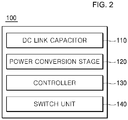
- FIG. 2 is a diagram for illustrating a photovoltaic inverter 100 according to an exemplary embodiment of the present disclosure.
- the photovoltaic inverter 100 according to an exemplary embodiment of the present disclosure includes a DC link capacitor 110, a power conversion stage 120, a controller 130, and a switch unit 140.
- the photovoltaic breaker 100 shown in FIG. 2 is merely an exemplary embodiment of the present disclosure, and the elements are not limited to those shown in FIG. 2 . Some elements may be added, modified or eliminated as desired.
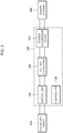
- FIG. 3 is a diagram for illustrating the photovoltaic inverter 100 according to the exemplary embodiment of the present disclosure connected to a solar cell array 310 and a power system 320.
- the photovoltaic inverter 100 and its elements i.e., the DC link capacitor 110, the power conversion stage 120, the controller 130, and the switch unit 140 will be described in detail with reference to FIGS. 2 and 3 .
- the DC link capacitor 110 stores a DC voltage output from the solar cell array 310. More specifically, the DC link capacitor 110 stores the DC voltage output from the solar cell array 310 and transmitted through the switch unit 140.
- the switch unit 140 may form a transmission path through which the DC voltage output from the solar cell array 310 is transmitted, which will be described later.
- the solar cell array 310 includes one or more solar cell panels connected in series or in parallel that produce electric energy using solar energy.
- the solar cell array 310 converts the light energy of incident sunlight into DC voltage and output it.
- the DC link capacitor 110 stores the DC voltage output from the solar cell array 310 having a voltage level equal to or greater than a predetermined level in order to supply the voltage to the power conversion stage 120, which will be described later.
- a DC/DC converter which is a step-up circuit, a switching regulator or the like may be disposed between the DC link capacitor 110 and the solar cell array 310.
- the DC link capacitor 110 may store a DC voltage of a predetermined level or more by smoothing the output voltage from the DC/DC converter, the switching regulator, and the like.
- the power conversion stage 120 generates AC power using the DC voltage stored in the DC link capacitor 110, and transmits the generated AC power to the power system 320. More specifically, the power conversion stage 120 converts the DC voltage stored in the DC link capacitor 110 into an alternating current by PWM (Pulse Width Modulation) control.
- PWM Pulse Width Modulation
- the power conversion stage 120 may further include a DC/DC converter for stepping up a DC voltage stored in the DC link capacitor 110, and the like.
- the power conversion stage 120 may convert the DC voltage stepped up by PWM (Pulse Width Modulation) control into alternating current.
- PWM Pulse Width Modulation
- the power system 320 may include a system in which generation and use of electric power is performed.
- the power system 320 may include any system that consumes power from a typical home to a large industrial facility.
- the controller 130 determines whether the driving value of the solar cell array 310 satisfies a predetermined driving condition.
- the controller 130 applies the DC voltage stored in the DC link capacitor 110 to the power conversion stage 120 based on the determination result.
- the controller 130 applies the reverse voltage of the DC voltage stored in the DC link capacitor 110 to the solar cell array 310 based on the determination result.
- the driving value of the solar cell array 310 includes at least one of the magnitude of the DC voltage output from the solar cell array 310, the driving time of the solar cell array 310, the driving time period of the solar cell array 310, and the intensity of polarization of the solar cell array 310.
- the driving time refers to the time at which the solar cell array 310 is currently driven
- the driving time period refers to a continuous time that elapsed since the solar cell array 310 has started being driven until the present time.
- the intensity of polarization [C/m 2 ] is a numerical value representing the amount of the polarized electric charge per unit area or the density of electric dipole moments induced per unit area.
- the driving condition is to drive the solar cell array 310, and may be set according to the driving value of the solar cell array 310. More specifically, if the driving value of the solar cell array 310 is the magnitude of the DC voltage output from the solar cell array 310, the driving condition may be a range of voltages for driving the solar cell array 310.
- the magnitude of the DC voltage output from the solar cell array 310 may be 600 V, and the driving condition, i.e., the range of the driving voltage may be 400 V or higher.
- the magnitude of the DC voltage is greater than 400 V, and thus the driving value of the solar cell array 310 can satisfy the driving condition.
- the driving condition can be satisfied when the driving time of the solar cell array 310 lies within a predetermined driving start time and a predetermined driving end time.
- the driving time of the solar cell array 310 is 5:30 pm
- the driving start time and the driving end time of the solar cell array 310 which are the driving condition, may be 10:00 am and 6:00 pm, respectively.
- the driving value of the solar cell array 310 can satisfy the driving condition of the solar cell array 310.
- the driving condition can be satisfied when the driving time period of the solar cell array 310 lies within a predetermined maximum driving time period.
- the driving time period of the solar cell array 310 is 12 hours, and the maximum driving time of the solar cell array 310, which is the driving condition, may be 10 hours. In this example, the driving time period is greater than 10 hours, the driving value of the solar cell array 310 may not satisfy the driving condition.
- the predetermined driving condition can be satisfied if the intensity of polarization of the solar cell array 310 lies within the range of the intensity of polarization for driving the solar cell array 310.
- the range of the intensity of polarization for driving the solar cell array 310 may be set to be less than a particular intensity of polarization.
- the range of the intensity of polarization may vary depending on the performance of the solar cell and the user's setting.
- the photovoltaic inverter may further include a voltage sensor, a timer, a device for measuring intensity of polarization, etc., for measuring the driving value of the solar cell array 310 described above.
- the controller 130 may apply the DC voltage stored in the DC link capacitor 110 to the power conversion stage 120.
- the controller 130 may apply a reverse voltage of the DC voltage stored in the DC link capacitor 110 to the solar cell array 310.
- the reverse voltage refers to a voltage having the same magnitude as and the opposite polarity to the DC voltage stored in the DC link capacitor 110. For example, if the DC voltage stored in the DC link capacitor 110 is +500 V, the reverse voltage is -500 V.
- the controller 130 controls the switch unit 140 so that the DC voltage stored in the DC link capacitor 110 is applied to the power conversion stage 120 or the reverse voltage of the DC voltage stored in the DC link capacitor 110 is applied to the solar cell array 310.
- the switch unit 140 controlled by the controller 130 will be described in detail with reference to FIGS. 4 to 7 .
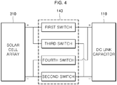
- FIG. 4 is a diagram for illustrating the switch unit connected between the solar cell array and the DC link capacitor according to an exemplary embodiment of the present disclosure.
- the switch unit 140 according to the exemplary embodiment of the present disclosure connects the positive terminal and the negative terminal of the solar cell array 310 to the positive terminal and the negative terminal or to the negative terminal and the positive terminal of the DC link capacitor 110, thereby forming a transmission path.
- the switch unit 140 includes a first switch connected between the positive terminal (+) of the solar cell array 310 and the positive terminal (+) of the DC link capacitor 110, a second switch connected between the negative terminal (-) of the solar cell array 310 and the negative terminal (-) of the DC link capacitor 110, a third switch connected between the positive terminal (+) of the solar cell array 310 and the negative terminal (-) of the DC link capacitor 110, and a fourth switch connected between the negative terminal (-) of the solar cell array 310 and the positive terminal (+) of the DC link capacitor 110.
- the first to fourth switches may be turned on or off by a control signal from the controller 130. They may be implemented using switching elements such as a gate turn-off thyristor (GTO), a bipolar junction transistor (BJT), a metal oxide silicon field effect transistor (MOSFET) and an IGBT (insulated gate bipolar mode transistor).
- GTO gate turn-off thyristor
- BJT bipolar junction transistor
- MOSFET metal oxide silicon field effect transistor
- IGBT insulated gate bipolar mode transistor
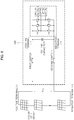
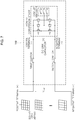
- FIG. 5 is a diagram illustrating a circuit in which the photovoltaic inverter 100 is connected to the solar cell array 310 according to an exemplary embodiment of the present disclosure.
- the photovoltaic inverter 100 may be configured such that the switch unit 140 including the first to fourth switches, the DC link capacitor 110 and the power conversion stage 120 share the positive terminal and the negative terminal.
- the positive terminal of the photovoltaic inverter 100 may be connected to the positive terminal and the negative terminal of the solar cell array 310 via the first switch and the fourth switch, respectively.
- the negative terminal of the photovoltaic inverter 100 may be connected to the negative terminal and the positive terminal of the solar cell array 310 via the second switch and the third switch, respectively.
- controller 130 may control the first to fourth switches to form a transmission path between the solar cell array 310 and the DC link capacitor 110.
- the power conversion stage 120 converts a DC voltage stored in the DC link capacitor 110 into alternating current by switching control such as PWM control to generate AC power.
- the power conversion stage 120 may include a plurality of switching elements.
- the power conversion stage 120 further includes a breaker connected to the power system 320 to transmit the generated AC power to the power system 320.
- FIG. 6 is a diagram for illustrating a circuit in a mode to apply a DC voltage stored in the DC link capacitor 110 to the power conversion stage 120.
- the driving value of the solar cell array 310 satisfies a predetermined driving condition, he controller 130 turns on the first switch and the second switch and turns off the third switch and the fourth switch.
- the controller 130 turns on the first and second switches and turns off the third and fourth switches, to form a transmission path.
- the positive terminal and the negative terminal of the solar cell array 310 may be connected to the positive terminal and the negative terminal of the DC link capacitor 110, respectively.
- the DC link capacitor 110 can store the DC voltage V DC output from the solar cell array 310.
- the power conversion stage 120 may convert the DC voltage V DC stored in the DC link capacitor 110 into AC power by the switching control and transmit the AC power to the power system 320 via the circuit breaker.
- FIG. 7 is a diagram illustrating a circuit configured to store an open-circuit voltage (V open ) output from the solar cell array 310 by the DC link capacitor 110 according to an exemplary embodiment of the present disclosure.
- FIG. 8 is a diagram for illustrating a circuit configured to apply a reverse voltage of the DC voltage stored in the DC link capacitor 110 to the solar cell array 310.
- the power conversion stage 120 may interrupt the AC power transmitted to the power system 320. More specifically, if the condition for driving the solar cell array 310 is not satisfied, the power conversion stage 120 may open the circuit breaker to interrupt the connection between the photovoltaic inverter 100 and the power system 320.
- the DC link capacitor 110 stores the open-circuit voltage V open output from the solar cell array 310.
- the internal circuit of the photovoltaic inverter 100 is an open circuit.
- the output voltage of the solar cell array 310 is the open-circuit voltage V open
- the DC link capacitor 110 stores the open-circuit voltage V open output from the solar cell array 310.
- the controller 130 may turn off the first switch and the second switch and turn on the third switch and the fourth switch.
- the positive terminal and the negative terminal of the solar cell array 310 may be connected to the negative terminal and the positive terminal of the DC link capacitor 110, respectively.
- the voltage dropped from the positive terminal of the solar cell array 310 to the negative terminal of the solar cell array 310 may be -V DC , which is the reverse voltage of the DC voltage V DC stored in the DC link capacitor 110. Therefore, when the reverse voltage is applied, the positive terminal of the solar cell array 310 has a potential lower than that of the negative terminal of the solar cell array 310.
- the internal circuit of the photovoltaic inverter 100 is an open circuit, as described above.
- the DC voltage V DC stored in the DC link is equal to the open-circuit voltage V open , and the voltage dropped from the positive terminal of the solar cell array 310 to the negative terminal of the photovoltaic cell array 310 is -V open .
- the open-circuit voltage V open is stored in the DC link capacitor 110. Then, when the controller 130 controls the switch unit 140 to form the transmission path as shown in FIG. 8 , the reverse voltage of the open-circuit voltage V open may be applied to the solar cell array 310.
- a reverse voltage can be applied to the solar cell array by controlling the switches connecting the solar cell array to the DC link capacitor with no separate module for applying the reverse voltage, thereby saving cost for establishing the photovoltaic system.
- the open-circuit voltage output from the solar cell array is not discharged but is used for reducing the polarization of the solar cell array, such that the residual energy of the photovoltaic power generation can be efficiently utilized.
- the controller 130 may control the DC voltage V DC so that the DC voltage V DC output from the solar cell array 310 tracks the maximum power of the solar cell array 310.
- the DC voltage V DC and the current output from the solar cell array 310 have nonlinear characteristics due to factors such as the material of the solar cell array 310. More specifically, the current output from the solar cell array 310 gradually decreases and then decreases sharply in a particular period, as the DC voltage V DC increases.
- the generated power of the solar cell array 310 with respect to the direct-current voltage V DC increases as the DC voltage V DC increases, and decreases sharply when the DC current voltage V DC exceeds a certain voltage.
- the amount of generated power of the solar cell array 310 can be the maximum value.
- the controller 130 may control the magnitude of the voltage V DC output from the solar cell array 310 so that it tracks the maximum power of the solar cell array 310 based on the electric characteristics of the solar cell array 310 (the maximum power point tracking (MPPT)).
- MPPT maximum power point tracking
- the method of controlling the magnitude of the DC voltage V DC output from the solar cell array 310 so that the amount of generated power of the solar cell array 310 tracks the maximum power may be performed according to various embodiments in the related art.
Landscapes
- Engineering & Computer Science (AREA)
- Power Engineering (AREA)
- Photovoltaic Devices (AREA)
- Inverter Devices (AREA)
- Charge And Discharge Circuits For Batteries Or The Like (AREA)
Claims (7)
- Onduleur photovoltaïque (100) destiné à appliquer une tension inverse à un réseau de cellules solaires (310), l'onduleur comprenant :un condensateur de liaison CC (110) configuré pour stocker une sortie de tension CC provenant du réseau de cellules solaires (310) ;un étage de conversion de puissance (120) configuré pour générer une puissance CA en utilisant la tension CC stockée dans le condensateur de liaison CC (110) afin de transmettre la puissance CA générée à un système de puissance (320) via un disjoncteur compris dans l'étage de conversion de puissance (120) ; etun dispositif de commande (130) configuré pour commander une unité de commutation (140) afin d'appliquer la tension CC stockée dans le condensateur de liaison CC (110) à l'étage de conversion de puissance (120) ou d'appliquer une tension inverse de la tension CC stockée dans le condensateur de liaison CC (110) au réseau de cellules solaires (310) en fonction du fait qu'une valeur d'entraînement du réseau de cellules solaires (310) satisfait ou non une condition d'entraînement prédéterminéecaractérisé en ce que l'onduleur photovoltaïque est configuré de sorte que l'étage de conversion de puissance (120) ouvre le disjoncteur pour stocker une tension de circuit ouvert (Vopen) du réseau de cellules solaires dans le condensateur de liaison CC (110) avant la commande par le dispositif de commande (130) de l'unité de commutation (140) pour appliquer la tension de circuit ouvert (Vopen) inverse du réseau de cellules solaires (310) stockée dans le condensateur de liaison CC au réseau de cellules solaires (310).
- Onduleur photovoltaïque (100) selon la revendication 1, dans lequel le dispositif de commande (130) est configuré pour appliquer la tension CC stockée dans le condensateur de liaison CC (110) à l'étage de conversion de puissance (120) si la valeur d'entraînement du réseau de cellules solaires (310) satisfait la condition d'entraînement prédéterminée, et dans lequel le dispositif de commande (130) est configuré pour appliquer la tension inverse de la tension CC stockée dans le condensateur de liaison CC (110) au réseau de cellules solaires (310) si la valeur d'entraînement du réseau de cellules solaires (310) ne satisfait pas la condition d'entraînement prédéterminée.
- Onduleur photovoltaïque (100) selon la revendication 1 ou 2, dans lequel l'étage de conversion de puissance (120) est configuré pour interrompre la puissance CA transmise au système de puissance (320) si la valeur d'entraînement du réseau de cellules solaires (310) ne satisfait pas la condition d'entraînement prédéterminée.
- Onduleur photovoltaïque (100) selon l'une quelconque des revendications 1 à 3, dans lequel le condensateur de liaison CC (110) est configuré pour stocker une sortie de tension de circuit ouvert provenant du réseau de cellules solaires (310) si la valeur d'entraînement du réseau de cellules solaires (310) ne satisfait pas la condition d'entraînement prédéterminée.
- Onduleur photovoltaïque (100) selon l'une quelconque des revendications 1 à 4, dans lequel la valeur d'entraînement du réseau de cellules solaires (310) comprend au moins un élément parmi : une amplitude de la sortie de tension CC provenant du réseau de cellules solaires (310), un moment d'entraînement du réseau de cellules solaires (310), une durée d'entraînement du réseau de cellules solaires (310) et une intensité de polarisation du réseau de cellules solaires (310).
- Onduleur photovoltaïque (100) selon l'une quelconque des revendications 1 à 5, dans lequel l'unité de commutation (140) comprend un premier commutateur connecté entre une borne positive du réseau de cellules solaires (310) et une borne positive du condensateur de liaison CC (110), un deuxième commutateur connecté entre une borne négative du réseau de cellules solaires (310) et une borne négative du condensateur de liaison CC (110), un troisième commutateur connecté entre la borne positive du réseau de cellules solaires (310) et la borne négative du condensateur de liaison CC (110) et un quatrième commutateur connecté entre la borne négative du réseau de cellules solaires (310) et la borne positive du condensateur de liaison CC (110).
- Onduleur photovoltaïque (100) selon la revendication 6, dans lequel le dispositif de commande (130) est configuré pour mettre en position de marche le premier commutateur et le deuxième commutateur et pour mettre en position d'arrêt le troisième commutateur et le quatrième commutateur si la valeur d'entraînement du réseau de cellules solaires (310) satisfait la condition d'entraînement prédéterminée, et dans lequel le dispositif de commande (130) est configuré pour mettre en position d'arrêt le premier commutateur et le deuxième commutateur et pour mettre en position de marche le troisième commutateur et le quatrième commutateur si la valeur d'entraînement du réseau de cellules solaires (310) ne satisfait pas la condition d'entraînement prédéterminée.
Applications Claiming Priority (1)
| Application Number | Priority Date | Filing Date | Title |
|---|---|---|---|
| KR1020160109839A KR20180024169A (ko) | 2016-08-29 | 2016-08-29 | 태양광 인버터 |
Publications (2)
| Publication Number | Publication Date |
|---|---|
| EP3291442A1 EP3291442A1 (fr) | 2018-03-07 |
| EP3291442B1 true EP3291442B1 (fr) | 2019-09-04 |
Family
ID=58714986
Family Applications (1)
| Application Number | Title | Priority Date | Filing Date |
|---|---|---|---|
| EP17171334.0A Active EP3291442B1 (fr) | 2016-08-29 | 2017-05-16 | Onduleur photovoltaique |
Country Status (6)
| Country | Link |
|---|---|
| US (1) | US10090754B2 (fr) |
| EP (1) | EP3291442B1 (fr) |
| JP (1) | JP6291111B2 (fr) |
| KR (1) | KR20180024169A (fr) |
| CN (1) | CN107809212B (fr) |
| ES (1) | ES2756707T3 (fr) |
Families Citing this family (9)
| Publication number | Priority date | Publication date | Assignee | Title |
|---|---|---|---|---|
| JP6711296B2 (ja) * | 2017-02-15 | 2020-06-17 | オムロン株式会社 | 電源システム、dc/dcコンバータ及びパワーコンディショナ |
| EP3567692B1 (fr) | 2018-05-10 | 2021-09-29 | Solaredge Technologies Ltd. | Appareil pour augmenter la fiabilité et la durée de vie de modules photovoltaïques (pv) |
| US11258261B2 (en) | 2018-05-10 | 2022-02-22 | Solaredge Technologies Ltd. | Systems and methods to increase the reliability and the service life time of photovoltaic (PV) modules |
| CN109742789B (zh) * | 2018-12-19 | 2022-05-20 | 广州金升阳科技有限公司 | 一种光伏发电系统 |
| KR102204955B1 (ko) | 2019-03-21 | 2021-01-19 | 주식회사 윌링스 | Pid 방지 기능을 갖는 태양광 발전시스템 |
| CN114285142A (zh) * | 2021-12-20 | 2022-04-05 | 珠海格力电器股份有限公司 | 光伏储能电路及其控制方法以及光伏空调系统和光伏空调 |
| WO2024064443A2 (fr) * | 2022-07-22 | 2024-03-28 | Lasermotive, Inc. | Électronique de récepteur de puissance |
| KR102582181B1 (ko) * | 2023-01-10 | 2023-10-04 | 주식회사 유환 | Ac차단과 dc차단을 연동한 효율유지형 태양광 발전장치 |
| KR102775222B1 (ko) | 2023-01-30 | 2025-03-04 | 한화솔루션 주식회사 | 전기커넥터 및 이를 포함하는 태양 전지 모듈용 인버터 |
Family Cites Families (27)
| Publication number | Priority date | Publication date | Assignee | Title |
|---|---|---|---|---|
| JP2002026356A (ja) * | 2000-07-04 | 2002-01-25 | Nissin Electric Co Ltd | 融雪装置 |
| ATE445254T1 (de) * | 2003-05-06 | 2009-10-15 | Enecsys Ltd | Stromversorgungsschaltungen |
| JP2005287136A (ja) * | 2004-03-29 | 2005-10-13 | Honda Motor Co Ltd | 平滑コンデンサのプリチャージ装置 |
| US7479774B2 (en) * | 2006-04-07 | 2009-01-20 | Yuan Ze University | High-performance solar photovoltaic (PV) energy conversion system |
| US20090078304A1 (en) * | 2007-09-26 | 2009-03-26 | Jack Arthur Gilmore | Photovoltaic charge abatement device, system, and method |
| US7964837B2 (en) * | 2007-12-31 | 2011-06-21 | Advanced Energy Industries, Inc. | Photovoltaic inverter interface device, system, and method |
| JP5377018B2 (ja) * | 2009-03-23 | 2013-12-25 | 株式会社東芝 | 太陽光発電システム |
| EP2325984A1 (fr) * | 2009-11-24 | 2011-05-25 | SMA Solar Technology AG | Démarrage d'un champ photovoltaïque avec haute tension à circuit ouvert |
| US8194375B2 (en) * | 2010-01-19 | 2012-06-05 | General Electric Company | Open circuit voltage protection system and method |
| US8836162B2 (en) * | 2010-02-26 | 2014-09-16 | Ziehl-Abegg Ag | Inverter for photovoltaic systems |
| US8395919B2 (en) * | 2010-07-29 | 2013-03-12 | General Electric Company | Photovoltaic inverter system and method of starting same at high open-circuit voltage |
| DE102010060633B3 (de) * | 2010-11-17 | 2012-04-26 | Sma Solar Technology Ag | Verfahren zum Verbinden einer Photovoltaikanlage mit einem Stromversorgungsnetz und Photovoltaikanlage zur Durchführung des Verfahrens |
| KR101732984B1 (ko) * | 2011-04-12 | 2017-05-08 | 엘지전자 주식회사 | 태양광 모듈 및 그 제어방법 |
| US9246330B2 (en) * | 2011-05-06 | 2016-01-26 | First Solar, Inc. | Photovoltaic device |
| US9343906B2 (en) * | 2011-06-03 | 2016-05-17 | Schneider Electric Solar Inverters Usa, Inc. | High dynamic DC-voltage controller for photovoltaic inverter |
| CN102544212A (zh) | 2011-12-31 | 2012-07-04 | 常州天合光能有限公司 | 太阳能组件功率衰减恢复方法 |
| DE102012101340B4 (de) * | 2012-02-20 | 2015-11-19 | Sma Solar Technology Ag | Schutz von Photovoltaikmodulen eines Photovoltaikgenerators vor Überspannungen gegenüber Erde |
| JP2014099438A (ja) * | 2012-11-13 | 2014-05-29 | Nisshinbo Mechatronics Inc | 太陽電池モジュールの出力低下予防回復装置および出力低下予防回復方法 |
| FR3000322B1 (fr) * | 2012-12-21 | 2016-05-20 | Schneider Electric Ind Sas | Dispositif de protection contre une surintensite electrique d'au moins une branche electronique de commutation, systeme de conversion comportant un tel dispositif de protection, et procede de pilotage associe |
| KR101442233B1 (ko) | 2013-03-08 | 2014-09-24 | 주식회사 루젠 | 태양전지모듈의 전력제어장치 |
| CN203166494U (zh) * | 2013-03-26 | 2013-08-28 | 阳光电源(上海)有限公司 | 一种解决电势诱导衰减的装置 |
| US10615607B2 (en) * | 2013-05-01 | 2020-04-07 | Tigo Energy, Inc. | Systems and methods for quick dissipation of stored energy from input capacitors of power inverters |
| KR20150030078A (ko) * | 2013-09-11 | 2015-03-19 | 엘에스산전 주식회사 | 태양광 인버터 |
| KR20160005613A (ko) | 2014-07-07 | 2016-01-15 | 주식회사 케이디파워 | 태양광 발전 시스템 |
| CN204068851U (zh) * | 2014-09-17 | 2014-12-31 | 英利能源(中国)有限公司 | 逆变器 |
| CN104333319B (zh) * | 2014-11-10 | 2017-12-22 | 许继电气股份有限公司 | 用于光伏并网逆变器的输入反接保护电路 |
| CN105720907B (zh) * | 2016-01-25 | 2018-02-23 | 南京科远自动化集团股份有限公司 | 一种用于逆变器中抑制光伏组件pid效应的方法及装置 |
-
2016
- 2016-08-29 KR KR1020160109839A patent/KR20180024169A/ko not_active Ceased
-
2017
- 2017-05-16 EP EP17171334.0A patent/EP3291442B1/fr active Active
- 2017-05-16 ES ES17171334T patent/ES2756707T3/es active Active
- 2017-05-18 JP JP2017099152A patent/JP6291111B2/ja active Active
- 2017-05-19 US US15/599,640 patent/US10090754B2/en active Active
- 2017-05-27 CN CN201710388084.4A patent/CN107809212B/zh active Active
Non-Patent Citations (1)
| Title |
|---|
| None * |
Also Published As
| Publication number | Publication date |
|---|---|
| CN107809212B (zh) | 2019-08-09 |
| US20180062502A1 (en) | 2018-03-01 |
| CN107809212A (zh) | 2018-03-16 |
| ES2756707T3 (es) | 2020-04-27 |
| JP2018038249A (ja) | 2018-03-08 |
| JP6291111B2 (ja) | 2018-03-14 |
| US10090754B2 (en) | 2018-10-02 |
| KR20180024169A (ko) | 2018-03-08 |
| EP3291442A1 (fr) | 2018-03-07 |
Similar Documents
| Publication | Publication Date | Title |
|---|---|---|
| US10090754B2 (en) | Photovoltaic inverter | |
| EP1039621B1 (fr) | Dispositif de génération d'énérgie photovoltaique | |
| US8513913B2 (en) | Photovoltaic system charge controller having buck converter with reversed MOSFETS | |
| US10720776B2 (en) | Optimal power collection control method and apparatus in solar photovoltaic power generation system | |
| US20130113452A1 (en) | System and Method for Power Conversion for Renewable Energy Sources | |
| CN1697282A (zh) | 电源装置以及该电源装置中所使用的控制方法 | |
| KR20150048875A (ko) | 하이브리드 저장 시스템들을 위한 토폴로지 및 제어 계획 | |
| US10396654B2 (en) | Start-up circuit | |
| US10283969B2 (en) | Solar photovoltaic output optimizer circuit | |
| KR20180111159A (ko) | 태양광 인버터 | |
| TW201532365A (zh) | 用於混合式儲存系統之拓撲及控制策略 | |
| JP2004336974A (ja) | 電源装置 | |
| KR101737461B1 (ko) | 태양전지에서 생성된 전력으로 제어 구동전원을 얻는 태양광 발전 시스템 및 그 방법 | |
| JP6489918B2 (ja) | 太陽エネルギーを含む複数のエネルギーによる電力供給装置 | |
| KR101661260B1 (ko) | 하이브리드 전원공급장치 | |
| CN103222181A (zh) | 光伏系统 | |
| KR102030934B1 (ko) | 신 재생에너지 파워 뱅크. | |
| CN119813352A (zh) | 一种基于直流母线电压信号的光储直流微网变换器协同控制系统 | |
| US11791732B2 (en) | Solar photovoltaic output optimizer circuit | |
| EP3079245B1 (fr) | Système et procédé de commande d'un dispositif de commutation intégré dans un convertisseur électronique et cellule de commutation comprenant ledit système | |
| KR101540796B1 (ko) | 충방전 제어 장치 | |
| KR101255470B1 (ko) | 에너지 저장 시스템 | |
| JPH0715870A (ja) | 太陽電池発電装置 | |
| KR200310557Y1 (ko) | 태양전지가 구비된 이엘용 인버터 | |
| SU1697248A1 (ru) | Электропривод посто нного тока |
Legal Events
| Date | Code | Title | Description |
|---|---|---|---|
| PUAI | Public reference made under article 153(3) epc to a published international application that has entered the european phase |
Free format text: ORIGINAL CODE: 0009012 |
|
| STAA | Information on the status of an ep patent application or granted ep patent |
Free format text: STATUS: THE APPLICATION HAS BEEN PUBLISHED |
|
| STAA | Information on the status of an ep patent application or granted ep patent |
Free format text: STATUS: REQUEST FOR EXAMINATION WAS MADE |
|
| AK | Designated contracting states |
Kind code of ref document: A1 Designated state(s): AL AT BE BG CH CY CZ DE DK EE ES FI FR GB GR HR HU IE IS IT LI LT LU LV MC MK MT NL NO PL PT RO RS SE SI SK SM TR |
|
| AX | Request for extension of the european patent |
Extension state: BA ME |
|
| STAA | Information on the status of an ep patent application or granted ep patent |
Free format text: STATUS: EXAMINATION IS IN PROGRESS |
|
| 17P | Request for examination filed |
Effective date: 20180226 |
|
| RBV | Designated contracting states (corrected) |
Designated state(s): AL AT BE BG CH CY CZ DE DK EE ES FI FR GB GR HR HU IE IS IT LI LT LU LV MC MK MT NL NO PL PT RO RS SE SI SK SM TR |
|
| 17Q | First examination report despatched |
Effective date: 20180329 |
|
| GRAP | Despatch of communication of intention to grant a patent |
Free format text: ORIGINAL CODE: EPIDOSNIGR1 |
|
| STAA | Information on the status of an ep patent application or granted ep patent |
Free format text: STATUS: GRANT OF PATENT IS INTENDED |
|
| INTG | Intention to grant announced |
Effective date: 20190430 |
|
| RIN1 | Information on inventor provided before grant (corrected) |
Inventor name: KIM, YOUNG-MIN |
|
| GRAS | Grant fee paid |
Free format text: ORIGINAL CODE: EPIDOSNIGR3 |
|
| GRAA | (expected) grant |
Free format text: ORIGINAL CODE: 0009210 |
|
| STAA | Information on the status of an ep patent application or granted ep patent |
Free format text: STATUS: THE PATENT HAS BEEN GRANTED |
|
| AK | Designated contracting states |
Kind code of ref document: B1 Designated state(s): AL AT BE BG CH CY CZ DE DK EE ES FI FR GB GR HR HU IE IS IT LI LT LU LV MC MK MT NL NO PL PT RO RS SE SI SK SM TR |
|
| REG | Reference to a national code |
Ref country code: GB Ref legal event code: FG4D |
|
| REG | Reference to a national code |
Ref country code: CH Ref legal event code: EP |
|
| REG | Reference to a national code |
Ref country code: AT Ref legal event code: REF Ref document number: 1176786 Country of ref document: AT Kind code of ref document: T Effective date: 20190915 |
|
| REG | Reference to a national code |
Ref country code: DE Ref legal event code: R096 Ref document number: 602017006651 Country of ref document: DE |
|
| REG | Reference to a national code |
Ref country code: IE Ref legal event code: FG4D |
|
| REG | Reference to a national code |
Ref country code: NL Ref legal event code: MP Effective date: 20190904 |
|
| REG | Reference to a national code |
Ref country code: LT Ref legal event code: MG4D |
|
| PG25 | Lapsed in a contracting state [announced via postgrant information from national office to epo] |
Ref country code: FI Free format text: LAPSE BECAUSE OF FAILURE TO SUBMIT A TRANSLATION OF THE DESCRIPTION OR TO PAY THE FEE WITHIN THE PRESCRIBED TIME-LIMIT Effective date: 20190904 Ref country code: SE Free format text: LAPSE BECAUSE OF FAILURE TO SUBMIT A TRANSLATION OF THE DESCRIPTION OR TO PAY THE FEE WITHIN THE PRESCRIBED TIME-LIMIT Effective date: 20190904 Ref country code: BG Free format text: LAPSE BECAUSE OF FAILURE TO SUBMIT A TRANSLATION OF THE DESCRIPTION OR TO PAY THE FEE WITHIN THE PRESCRIBED TIME-LIMIT Effective date: 20191204 Ref country code: HR Free format text: LAPSE BECAUSE OF FAILURE TO SUBMIT A TRANSLATION OF THE DESCRIPTION OR TO PAY THE FEE WITHIN THE PRESCRIBED TIME-LIMIT Effective date: 20190904 Ref country code: NO Free format text: LAPSE BECAUSE OF FAILURE TO SUBMIT A TRANSLATION OF THE DESCRIPTION OR TO PAY THE FEE WITHIN THE PRESCRIBED TIME-LIMIT Effective date: 20191204 Ref country code: LT Free format text: LAPSE BECAUSE OF FAILURE TO SUBMIT A TRANSLATION OF THE DESCRIPTION OR TO PAY THE FEE WITHIN THE PRESCRIBED TIME-LIMIT Effective date: 20190904 |
|
| PG25 | Lapsed in a contracting state [announced via postgrant information from national office to epo] |
Ref country code: LV Free format text: LAPSE BECAUSE OF FAILURE TO SUBMIT A TRANSLATION OF THE DESCRIPTION OR TO PAY THE FEE WITHIN THE PRESCRIBED TIME-LIMIT Effective date: 20190904 Ref country code: GR Free format text: LAPSE BECAUSE OF FAILURE TO SUBMIT A TRANSLATION OF THE DESCRIPTION OR TO PAY THE FEE WITHIN THE PRESCRIBED TIME-LIMIT Effective date: 20191205 Ref country code: AL Free format text: LAPSE BECAUSE OF FAILURE TO SUBMIT A TRANSLATION OF THE DESCRIPTION OR TO PAY THE FEE WITHIN THE PRESCRIBED TIME-LIMIT Effective date: 20190904 Ref country code: RS Free format text: LAPSE BECAUSE OF FAILURE TO SUBMIT A TRANSLATION OF THE DESCRIPTION OR TO PAY THE FEE WITHIN THE PRESCRIBED TIME-LIMIT Effective date: 20190904 |
|
| REG | Reference to a national code |
Ref country code: AT Ref legal event code: MK05 Ref document number: 1176786 Country of ref document: AT Kind code of ref document: T Effective date: 20190904 |
|
| REG | Reference to a national code |
Ref country code: ES Ref legal event code: FG2A Ref document number: 2756707 Country of ref document: ES Kind code of ref document: T3 Effective date: 20200427 |
|
| PG25 | Lapsed in a contracting state [announced via postgrant information from national office to epo] |
Ref country code: RO Free format text: LAPSE BECAUSE OF FAILURE TO SUBMIT A TRANSLATION OF THE DESCRIPTION OR TO PAY THE FEE WITHIN THE PRESCRIBED TIME-LIMIT Effective date: 20190904 Ref country code: EE Free format text: LAPSE BECAUSE OF FAILURE TO SUBMIT A TRANSLATION OF THE DESCRIPTION OR TO PAY THE FEE WITHIN THE PRESCRIBED TIME-LIMIT Effective date: 20190904 Ref country code: NL Free format text: LAPSE BECAUSE OF FAILURE TO SUBMIT A TRANSLATION OF THE DESCRIPTION OR TO PAY THE FEE WITHIN THE PRESCRIBED TIME-LIMIT Effective date: 20190904 Ref country code: PL Free format text: LAPSE BECAUSE OF FAILURE TO SUBMIT A TRANSLATION OF THE DESCRIPTION OR TO PAY THE FEE WITHIN THE PRESCRIBED TIME-LIMIT Effective date: 20190904 Ref country code: PT Free format text: LAPSE BECAUSE OF FAILURE TO SUBMIT A TRANSLATION OF THE DESCRIPTION OR TO PAY THE FEE WITHIN THE PRESCRIBED TIME-LIMIT Effective date: 20200106 Ref country code: AT Free format text: LAPSE BECAUSE OF FAILURE TO SUBMIT A TRANSLATION OF THE DESCRIPTION OR TO PAY THE FEE WITHIN THE PRESCRIBED TIME-LIMIT Effective date: 20190904 |
|
| PG25 | Lapsed in a contracting state [announced via postgrant information from national office to epo] |
Ref country code: SK Free format text: LAPSE BECAUSE OF FAILURE TO SUBMIT A TRANSLATION OF THE DESCRIPTION OR TO PAY THE FEE WITHIN THE PRESCRIBED TIME-LIMIT Effective date: 20190904 Ref country code: CZ Free format text: LAPSE BECAUSE OF FAILURE TO SUBMIT A TRANSLATION OF THE DESCRIPTION OR TO PAY THE FEE WITHIN THE PRESCRIBED TIME-LIMIT Effective date: 20190904 Ref country code: IS Free format text: LAPSE BECAUSE OF FAILURE TO SUBMIT A TRANSLATION OF THE DESCRIPTION OR TO PAY THE FEE WITHIN THE PRESCRIBED TIME-LIMIT Effective date: 20200224 Ref country code: SM Free format text: LAPSE BECAUSE OF FAILURE TO SUBMIT A TRANSLATION OF THE DESCRIPTION OR TO PAY THE FEE WITHIN THE PRESCRIBED TIME-LIMIT Effective date: 20190904 |
|
| REG | Reference to a national code |
Ref country code: DE Ref legal event code: R097 Ref document number: 602017006651 Country of ref document: DE |
|
| PLBE | No opposition filed within time limit |
Free format text: ORIGINAL CODE: 0009261 |
|
| STAA | Information on the status of an ep patent application or granted ep patent |
Free format text: STATUS: NO OPPOSITION FILED WITHIN TIME LIMIT |
|
| PG2D | Information on lapse in contracting state deleted |
Ref country code: IS |
|
| PG25 | Lapsed in a contracting state [announced via postgrant information from national office to epo] |
Ref country code: DK Free format text: LAPSE BECAUSE OF FAILURE TO SUBMIT A TRANSLATION OF THE DESCRIPTION OR TO PAY THE FEE WITHIN THE PRESCRIBED TIME-LIMIT Effective date: 20190904 Ref country code: IS Free format text: LAPSE BECAUSE OF FAILURE TO SUBMIT A TRANSLATION OF THE DESCRIPTION OR TO PAY THE FEE WITHIN THE PRESCRIBED TIME-LIMIT Effective date: 20200105 |
|
| 26N | No opposition filed |
Effective date: 20200605 |
|
| PG25 | Lapsed in a contracting state [announced via postgrant information from national office to epo] |
Ref country code: SI Free format text: LAPSE BECAUSE OF FAILURE TO SUBMIT A TRANSLATION OF THE DESCRIPTION OR TO PAY THE FEE WITHIN THE PRESCRIBED TIME-LIMIT Effective date: 20190904 |
|
| PG25 | Lapsed in a contracting state [announced via postgrant information from national office to epo] |
Ref country code: CH Free format text: LAPSE BECAUSE OF NON-PAYMENT OF DUE FEES Effective date: 20200531 Ref country code: LI Free format text: LAPSE BECAUSE OF NON-PAYMENT OF DUE FEES Effective date: 20200531 Ref country code: MC Free format text: LAPSE BECAUSE OF FAILURE TO SUBMIT A TRANSLATION OF THE DESCRIPTION OR TO PAY THE FEE WITHIN THE PRESCRIBED TIME-LIMIT Effective date: 20190904 |
|
| REG | Reference to a national code |
Ref country code: BE Ref legal event code: MM Effective date: 20200531 |
|
| PG25 | Lapsed in a contracting state [announced via postgrant information from national office to epo] |
Ref country code: LU Free format text: LAPSE BECAUSE OF NON-PAYMENT OF DUE FEES Effective date: 20200516 |
|
| PG25 | Lapsed in a contracting state [announced via postgrant information from national office to epo] |
Ref country code: IE Free format text: LAPSE BECAUSE OF NON-PAYMENT OF DUE FEES Effective date: 20200516 |
|
| PG25 | Lapsed in a contracting state [announced via postgrant information from national office to epo] |
Ref country code: BE Free format text: LAPSE BECAUSE OF NON-PAYMENT OF DUE FEES Effective date: 20200531 |
|
| PG25 | Lapsed in a contracting state [announced via postgrant information from national office to epo] |
Ref country code: TR Free format text: LAPSE BECAUSE OF FAILURE TO SUBMIT A TRANSLATION OF THE DESCRIPTION OR TO PAY THE FEE WITHIN THE PRESCRIBED TIME-LIMIT Effective date: 20190904 Ref country code: MT Free format text: LAPSE BECAUSE OF FAILURE TO SUBMIT A TRANSLATION OF THE DESCRIPTION OR TO PAY THE FEE WITHIN THE PRESCRIBED TIME-LIMIT Effective date: 20190904 Ref country code: CY Free format text: LAPSE BECAUSE OF FAILURE TO SUBMIT A TRANSLATION OF THE DESCRIPTION OR TO PAY THE FEE WITHIN THE PRESCRIBED TIME-LIMIT Effective date: 20190904 |
|
| PG25 | Lapsed in a contracting state [announced via postgrant information from national office to epo] |
Ref country code: MK Free format text: LAPSE BECAUSE OF FAILURE TO SUBMIT A TRANSLATION OF THE DESCRIPTION OR TO PAY THE FEE WITHIN THE PRESCRIBED TIME-LIMIT Effective date: 20190904 |
|
| P01 | Opt-out of the competence of the unified patent court (upc) registered |
Effective date: 20230625 |
|
| PGFP | Annual fee paid to national office [announced via postgrant information from national office to epo] |
Ref country code: GB Payment date: 20260309 Year of fee payment: 10 |
|
| PGFP | Annual fee paid to national office [announced via postgrant information from national office to epo] |
Ref country code: IT Payment date: 20260306 Year of fee payment: 10 |
|
| PGFP | Annual fee paid to national office [announced via postgrant information from national office to epo] |
Ref country code: FR Payment date: 20260309 Year of fee payment: 10 |
|
| PGFP | Annual fee paid to national office [announced via postgrant information from national office to epo] |
Ref country code: ES Payment date: 20260608 Year of fee payment: 10 |
|
| PGFP | Annual fee paid to national office [announced via postgrant information from national office to epo] |
Ref country code: DE Payment date: 20260305 Year of fee payment: 10 |