EP3291464B1 - Verfahren und vorrichtung zum optischen senden zur erzeugung eines optischen binären digitalen sendesignals - Google Patents
Verfahren und vorrichtung zum optischen senden zur erzeugung eines optischen binären digitalen sendesignals Download PDFInfo
- Publication number
- EP3291464B1 EP3291464B1 EP16187142.1A EP16187142A EP3291464B1 EP 3291464 B1 EP3291464 B1 EP 3291464B1 EP 16187142 A EP16187142 A EP 16187142A EP 3291464 B1 EP3291464 B1 EP 3291464B1
- Authority
- EP
- European Patent Office
- Prior art keywords
- optical
- signal
- binary digital
- optical transmitter
- transmitter
- Prior art date
- Legal status (The legal status is an assumption and is not a legal conclusion. Google has not performed a legal analysis and makes no representation as to the accuracy of the status listed.)
- Active
Links
Images


Classifications
-
- H—ELECTRICITY
- H04—ELECTRIC COMMUNICATION TECHNIQUE
- H04B—TRANSMISSION
- H04B10/00—Transmission systems employing electromagnetic waves other than radio-waves, e.g. infrared, visible or ultraviolet light, or employing corpuscular radiation, e.g. quantum communication
- H04B10/50—Transmitters
- H04B10/516—Details of coding or modulation
-
- H—ELECTRICITY
- H04—ELECTRIC COMMUNICATION TECHNIQUE
- H04B—TRANSMISSION
- H04B10/00—Transmission systems employing electromagnetic waves other than radio-waves, e.g. infrared, visible or ultraviolet light, or employing corpuscular radiation, e.g. quantum communication
- H04B10/50—Transmitters
- H04B10/501—Structural aspects
- H04B10/503—Laser transmitters
- H04B10/504—Laser transmitters using direct modulation
-
- H—ELECTRICITY
- H04—ELECTRIC COMMUNICATION TECHNIQUE
- H04B—TRANSMISSION
- H04B10/00—Transmission systems employing electromagnetic waves other than radio-waves, e.g. infrared, visible or ultraviolet light, or employing corpuscular radiation, e.g. quantum communication
- H04B10/50—Transmitters
- H04B10/516—Details of coding or modulation
- H04B10/548—Phase or frequency modulation
- H04B10/556—Digital modulation, e.g. differential phase shift keying [DPSK] or frequency shift keying [FSK]
-
- H—ELECTRICITY
- H04—ELECTRIC COMMUNICATION TECHNIQUE
- H04J—MULTIPLEX COMMUNICATION
- H04J14/00—Optical multiplex systems
- H04J14/02—Wavelength-division multiplex systems
Definitions
- the present invention relates to a method for creating an optical binary digital transmit signal exploiting intentional mode hops comprising the pre-characterizing features of claim 1 and to an optical transmitter device for creating at least one optical binary digital transmit signal to be supplied to an optical transmission link for realizing this method comprising the pre-characterizing features of claim 5.
- Semiconductor lasers are mainly used as electro-optical conversion elements in optical transmitters. Direct modulation of a semiconductor laser induces chirp, that is dynamic wavelength changes, during modulation. This results in an undesired broadening of the optical signal spectrum and, in turn, to a reduced chromatic dispersion tolerance of a digital optical transmit signal that is created in this way.
- modulating a semiconductor laser for example a DFB or DBR laser, at a modulation rate (symbol rate) of 10 Gb/s (10 GBaud) results in a dispersion tolerance corresponding to 10 km or less when using a standard single mode fiber (according to Recommendation ITU-T G.652) in the 1550 nm wavelength range.
- phase modulation can be controlled and can be reduced to zero, leaving amplitude modulation of the optical carrier only.
- the interaction current of a DFB laser is modulated with a small amplitude.
- This method is known as "chirp managed laser” and results in a relatively small extinction ratio and a frequency shift of the optical signals between mark and space bits on the order of half the modulation data rate.
- a steep-edged optical filter is required, which suppresses the power in the space bits in order to increase the extinction ratio and to reduce the spectral width of the modulated optical signal.
- This method requires a costly optical filter and a tight control of the temperature of the laser in order to exactly match the laser wavelength with the edge of the optical filter.
- the US patent US 5 243 608 describes an optical transmission process by wavelength shifting and a corresponding system.
- intentional wavelength hopping or mode hopping is used in order to create a modulated optical binary digital transmit signal which is supplied to an optical transmission link.
- This modulation technique is called wavelength shift (WSK).
- the wavelength shift is obtained by a careful choice of the currents injected into the multiple-section semiconductor structures of the semiconductor lasers.
- the complete modulated signal is supplied to the optical transmission link and received, at the receiver side, by direct detection, wherein prior to the opto-electrical conversion elements an optical band-pass filter is used, in order to extract from the optical signal received the wavelength range comprising the center wavelength of a selected one of the modes between which the mode hopping occurs.
- dispersion introduced by the optical transmission link influences the transmission quality and thus the bit error rate of a respective transmission system.
- WDM optical wavelength division multiplex
- an optical transmitter is operated in such a state that mode hopping occurs between a predefined first and a predefined second optical mode of the optical transmitter if a binary digital modulation signal is supplied to the optical transmitter device.
- a modulated optical output signal output by the optical transmitter is created, which corresponds to the binary digital modulation signal supplied to the optical transmitter, wherein a first state of the binary digital modulation signal leads to an optical output signal at a center wavelength of the first optical mode and a second state of the binary digital modulation signal leads to an optical output signal at a center wavelength of the second optical mode.
- the modulated optical output signal is filtered in such a way that at least a portion of the optical power spectrum of the modulated optical output signal caused by a selected one of the first and second optical modes is suppressed or at least substantially attenuated.
- the dispersion introduced by the optical transmission link especially by an optical fiber, cannot affect filtered signal portions comprising the center frequency of the respective (filtered) mode and the spectral components depending on the binary digital modulation signal. This leads to an improved extinction ratio of the detected receive signal as compared to the method disclosed in US 5 243 608 , according to which an optical band-pass filter is provided in the reception module.
- At least substantially attenuating a portion of the optical power spectrum of the modulated optical output signal caused by a selected one of the first and second optical modes means that the filtered signal, i.e. the optical binary digital transmit signal to be supplied to the optical transmission link, has a substantially lower peak in the optical power spectrum than the peak caused by the non-selected optical mode.
- a “substantially lower peak” means that the signal directly detected by the receiver reveals a sufficiently high extinction ratio.
- the optical mode causing a lower peak in the optical power spectrum is selected for effecting the optical filtering of the modulated optical output signal. This leads to a better extinction ratio as compared to selecting the mode causing the higher peak.
- the mode hopping effect is essentially caused or influenced by two parameters, which both depend on the gain current I gain , namely the temperature and the charge carrier density in the active region of the semiconductor laser 3. Both parameters influence the phase.
- the "charge carrier effect” is dominant for higher bit rates, e.g. for bit rates above 4 to 6 Gbit/s depending on the design of the semiconductor laser.
- the "temperature effect” is dominant in for lower bit rates, e.g below 4 to 6 Gb/s.
- a stepwise transition occurs between the mode representing the actual (mark or space) bit and the mode representing the following (space or mark) bit, wherein also the one or more intermediate modes, which do not represent a valid bit in the binary modulating signal S mod , exist for a given short time (significantly smaller than the bit interval).
- applying an optical filtering at the transmitter side in such a way that merely the optical spectrum of one of the modes (which are assigned to the two states of the binary optical modulation signal) is transmitted (whereas the rest of the spectrum is suppressed or at least sufficiently attenuated) results in an enhanced extinction ratio.
- the design of the optical filter is simplified.
- an optical filter device is used for optically filtering the modulated optical output signal, which defines a channel bandwidth of the optical transmission link that is assigned to the optical binary digital transmit signal.
- an optical channel filter is already present in an optical transmission system, which provides an optical channel having a restricted optical bandwidth only for transmitting an optical signal.
- the method according to the invention does, in such a case, not require any additional optical filter and can be implemented at low costs.
- the optical filter device can be realized as a wavelength division multiplexer means, which is adapted to optically filter multiplex a plurality of modulated optical output signal. That is, in an optical WDM transmission system or an optical WDM transmitter device, respectively, the multiplexer means may simultaneously be used as an optical band-pass filter for filtering a modulated optical output signal that is created according to the present invention in order to obtain the desired optical binary digital transmit signal (including the mode hopping modulation) to be supplied to an optical transmission link.
- the multiplexer means must reveal a suitable band-pass filtering characteristic.
- An optical transmitter device comprises at least one optical transmitter configured to operate in or configured to be controllable to operate in a mode-hopping state, in which mode hopping occurs between a predefined first and a predefined second optical mode of the optical transmitter depending on a first and a second state of a binary digital modulation signal supplied to the at least one optical transmitter, and a control device supplying a dedicated binary digital modulation signal to each of the at least one optical transmitters, wherein each of the at least one optical transmitters and the control device are configured to create a modulated optical output signal corresponding to the binary digital modulation signal, wherein a first state of the binary digital modulation signal leads to a modulated optical output signal at a center wavelength of the first optical mode and a second state of the binary digital modulation signal leads to an optical output signal at a center wavelength of the second optical mode.
- the optical transmitter device further comprises at least one optical filter device configured to optically filter each of the at least one modulated optical output signals in such a way that at least a portion of the optical power spectrum of the modulated optical output signal caused by a selected one of the first and second optical modes is suppressed or at least substantially attenuated.
- a suitable optical transmitter may be configured to operate, without the need of supplying additional control signals, in a mode-hopping state, whenever a suitable binary digital modulation signal is supplied to the at least one optical transmitter.
- a suitable binary digital modulation signal may be supplied to the at least one optical transmitter.
- the modulation signal may be a modulation current including a bias current for adjusting the operation point of a semiconductor laser that is used as an optical transmitter.
- the control device may not only be configured to provide a dedicated binary digital modulation signal, but also dedicated control signals for establishing the mode-hopping state to each of the at least one optical transmitters.
- the control device may be realized as a single central device or as a distributed device comprising a respective number of sub-devices, each of which is assigned to one of the optical transmitters.
- a central control device may comprise a first sub-device for creating and/or supplying the control signal(s) to the optical transmitters and a second sub-device for creating and/or supplying the binary digital modulation signals to the optical transmitters.
- the sub-devices of a distributed control device may be realized, i.e. each sub-device comprises a first sub-device for creating and/or supplying the control signal to the respective optical transmitters and a second sub-device for creating and/or supplying the binary digital modulation signal to the respective optical transmitters.
- the at least one optical transmitter is a tunable optical transmitter and the control device is configured to supply at least one state control signal to the at least one optical transmitter, wherein the at least one control signal controls the at least one optical transmitter to operate in a predefined mode hopping state, in which mode hopping occurs between a predefined first and a predefined second optical mode having a first and a second center wavelength, respectively.
- the tunable optical transmitter may be or may comprise a tunable semiconductor laser, preferably a semiconductor laser having a multi-section structure, such as a distributed feed-back (DFB) laser, a distributed Bragg reflector (DBR) laser, a sampled grating DBR (SG-DBR) laser or a Y-branch laser etc.
- DFB distributed feed-back
- DBR distributed Bragg reflector
- SG-DBR sampled grating DBR
- An optical WDM transmitter device comprises a plurality of optical transmitters, each creating a respective modulated optical output signal, each of which having an optical power spectrum comprising a peak at a center wavelength of a respective mode, which is different from the center wavelengths of the two modes of any of the other modulated optical output signals.
- the optical filter device of such an optical WDM transmitter device may comprise a separate optical filter for each of the at least one optical transmitters, wherein each optical transmitter and each dedicated optical filter are configured to create a respective optical binary digital transmit signal at a predetermined center wavelength differing from the center wavelengths of the optical binary digital transmit signals created by any other pair of an optical transmitter and a dedicated optical filter.
- the filtered optical binary digital transmit signals i.e.
- the optical binary transmission digital signals are supplied to an optical multiplexer device, which is configured to combine these signals to an optical WDM transmit signal.
- the optical multiplexer device may be realized as a simple optical combiner device, i.e. a 1 x N optical splitter/combiner, which outputs the optical WDM transmit signal at a WDM port.
- an optical WDM transmitter device comprising a plurality of optical transmitters may comprise an optical filter device that is realized as an optical multiplexer and filter device, which is configured to create an optical WDM transmit signal by filtering and simultaneously combining the modulated optical output signals created by the optical transmitters and supplied to respective dedicated channel ports of the optical filter device.
- the optical WDM transmit signal comprises a plurality of filtered modulated optical output signals, which are created by the plurality of optical transmitters, as optical channel signals.
- Such an optical multiplexer and filter device may be realized as an arrayed waveguide grating or any other device having the functionality of an arrayed waveguide grating.
- the least one optical transmitter comprises an electrical high-pass filter configured to electrically high-pass filter the binary digital modulation signal before it is supplied to the tunable semiconductor laser.
- an electrical high-pass filter configured to electrically high-pass filter the binary digital modulation signal before it is supplied to the tunable semiconductor laser.
- this modulation method which is, for example, known from US 5 243 608 , shall be briefly explained with reference to Figs. 1 to 3 .
- Fig. 1 schematically shows a block diagram of the structure of an optical transmitter element 1 in the form of a widely tunable semiconductor laser 3.
- This semiconductor laser 3 comprises a broadband grating section 5, a gain section 7 and a front reflector section 9, which define the phase matching condition of the laser cavity.
- the broadband grating section 5, which realizes a rear reflector of the laser cavity, is a broadband grating having a spectral reflectivity according to the dashed line in Fig. 2a .
- the spectral reflectivity of the broadband grating section 5 reveals a peak at a predetermined wavelength.
- This peak wavelength can be shifted by supplying a first control signal 11 to the broadband grating section 5 in the form of a grating current I graiting having a predetermined value or state. Varying the control signal 11 within a predetermined range causes a shift of the peak wavelength within a corresponding large wavelength range. Accordingly, the center wavelength of an optical signal created by the optical transmitter element 1 can be controlled to reach a predetermined value within a given wavelength range by supplying a control signal 11 having a corresponding predetermined value or, generally speaking, having a corresponding predetermined state.
- the front reflector section 9 is configured in such a way that it influences the phase matching condition of the laser cavity depending on a second control signal 13 in the form of a phase current I phase supplied to the front reflector section.
- the filter function of the laser cavity which is determined by the state of the front section, is depicted as solid line in Fig. 2a .
- This comb-shaped filter function reveals a plurality of peaks essentially having the same height and an essentially constant frequency separation. Each center wavelength of a peak of this filter function corresponds to a longitudinal mode of the optical transmitter element 1.
- the phase spectrum of this filter function can be shifted in a desired manner by supplying a control signal 13 having a predetermined value or, generally speaking, a predetermined state.
- the (spectral) filter function according to the solid line can be shifted in a desired manner by supplying a grating current I phase having a predetermined value or, generally speaking, a predetermined state.
- Fig. 2b shows the combined spectral reflections of the broadband grating section 5 and the front reflector section 9, which approximately corresponds to the products of the two single spectra.
- the center wavelength of the optical signal created by the optical transmitter element 1 or the semiconductor laser 3, respectively, corresponds to the longitudinal mode of the optical transmitter element 1 which is best reflected. That is, the center wavelength of the optical signal created corresponds to the center wavelength of the longitudinal mode having the highest peak in the combined reflectivity curve shown by the solid line in Fig. 2b (the dashed line in Fig. 2b , on which the peak points lie, essentially corresponds to the spectral reflectivity of the broadband grating section 5 in Fig. 2a ).
- the optical transmitter element 1 in the first state of the optical transmitter element 1 defined by a respective first value or state of the first and second control signals 11, 13 (i.e. a first value or state of the currents I grating and I phase ) and shown in Figs. 2a and 2b , the optical transmitter element 1 emits at a wavelength corresponding to the center wavelength of the peak shown in black, which, in this state, corresponds to the longitudinal mode which is reflected with the maximum combined reflectivity at the rear and front sections 5, 9.
- a respective first value or state of the first and second control signals 11, 13 i.e. a first value or state of the currents I grating and I phase
- the filter function according to the solid line in Fig. 2 is shifted if the gain signal changes its value or, generally speaking, its state.
- the gain signal has changed its value or state in such a way that the filter function (again shown as a solid line in Fig. 3b ) is shifted to the right (indicated by the arrow in Fig. 3a ), whereas the spectral reflectivity of the broadband grating section 5 (again shown as a dashed line in Fig. 3a ) remains unchanged.
- a change between two modes depending on two corresponding differing states of a binary digital modulation signal may be used to modulate the center wavelength of the optical signal created by the optical transmitter element 1.
- This binary digital modulation signal may be supplied to the optical transmitter element 1 as a gain current I gain .
- the gain current I gain may include, especially as an additive component, a current for controlling the operating point of the optical transmitter element 1 or the semiconductor laser 3, respectively.
- Such a modulated optical output signal of the optical transmitter element 1 may be supplied to an optical transmission link.
- the signal may be directly detected after optically filtering the optical signal in such a way that the spectral portion or the spectral components created at a selected mode are essentially suppressed.
- this modulated signal has a spectral power density as exemplarily shown in Fig. 4 .
- This optical spectrum essentially reveals two peaks around the center wavelengths of the two modes that are used for the mode hopping modulation.
- both spectral ranges around these peaks comprise the full information included in the binary digital modulation signal as each of the peaks either corresponds to the mark bits (i.e. 1 bits) or the space bits (i.e. 0 bits) thereof.
- the mark bits of the modulated signal are usually created by a higher level of the gain current that is supplied to the respective optical transmitter (e.g. to a multi-section semiconductor laser) than the space bits, it would generally be possible to directly detect this signal as the optical power of the mark bits is higher than the optical power of the space bits.
- the extinction ratio can be increased if the selected one of the spectral ranges surrounding the center wavelengths of the respective two modes is suppressed or attenuated in such a way that the optical power included in a signal portion representing a space (or mark) bit is sufficiently lower than the optical power included in a signal portion representing a marked (or space) bit.
- an optical bandpass filter is used at the receiver side in order to increase the extinction ratio.
- the filter output signal corresponds either to the binary digital modulation signal or to its complement, i.e. to the inverted binary digital modulation signal.
- the two signals represented by the two peaks of the optical power spectrum of the modulated signal are complementary signals
- the peak having the lower peak value corresponds to the complementary signal having a lower extinction ratio than the respective other complementary signal. It is therefore generally advantageous to choose the filter bandwidth of the bandpass filter in such a way that the spectral range surrounding the peak having the lower peak value is suppressed or sufficiently attenuated.
- an optical bandpass filter should be designed in such a way that the spectral peak having a center wavelength of approximately 1564.4 nm revealing the higher peak value is passed through.
- the filter bandwidth should be selected in such a way that the signal portions created by the modulation (generally both sidebands) are also passed through.
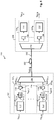
- Fig. 5 shows an optical single-channel transmission system 100 comprising a (single-channel) optical transmitter device 102 and a (single channel) optical receiver device 104, which are connected to a respective end of an optical transmission link 106 that may be realized as an optical fiber, for example a standard single-mode fiber.
- the optical transmitter device 102 is configured to receive a digital transmit signal S TX at an input port thereof and to create an optical binary digital transmit signal SMH TX , (including the information of the digital transmit signal S TX ), which is supplied to the respective end of the optical transmission link 106.
- This optical binary digital transmit signal SMH TX is transmitted from the near and of the optical transmission link 106 to the far end thereof and is received at the far end by the receiver device 104 as an optical binary digital receive signal SMH RX .
- the receiver device 104 is configured to directly receive the optical binary digital receive signal SMH RX that is supplied to an input port thereof.
- the optical receiver device 104 comprises an opto-electrical converter 108, such as a photodiode, and a signal processing unit 110.
- the opto-electrical converter 108 converts the optical transmit signal received S RX into a respective electrical receive signal.
- the electrical receive signal is supplied to the input port of the signal processing unit 110 for further processing. This further processing may include signal regeneration in order to create a digital receive signal S RX including the information that has been transmitted.
- the optical transmitter device 102 may be adapted to receive an electrical or optical transmit signal S TX at a respective input port.
- the receiver device 104 may be configured to output the receive signal S RX in the form of an electrical or optical signal.
- the optical transmitter device 102 comprises a control device, an optical transmitter element 114 and an optical filter device 116 comprising an optical bandpass filter 118.
- the control device is configured to control the optical transmitter in such a way that it operates in a mode hopping state, in which mode hopping occurs between a predefined first and a predefined second optical mode of the optical transmitter if a binary digital modulation signal S mod is supplied to the optical transmitter element 114.
- the control device creates one or more control signals S CTR , which are supplied to the optical transmitter element 114.
- the optical transmitter element 114 may be realized or may comprise a multi-section structure semiconductor laser 1 and the control signals may comprise a first control signal 11 in the form of a grating current I grating and a second control signal 13 in the form of a phase current I phase .
- a further, third control signal may be comprised by a modulation signal S mod , which is supplied to a modulation port of the optical transmitter element 114.
- a constant or controllably and slowly varying portion or component of the gain current I gain may determine the operating point and thus also the mode hopping state of the optical transmitter device 114.
- a further portion or component of the gain current I gain constitutes the desired binary digital modulation signal S mod .
- control signals are designated by the reference sign S CTR irrespective of whether a specific control signal is separately supplied to the transmitter 114 or as a component of the binary digital modulation signal S mod and the reference sign S mod designates the binary digital modulation signal irrespective of whether this signal, in addition to a mere modulation component, comprises a component which constitutes a control signal.
- the control signals S CTR and the binary digital modulation signal S mod cause the optical transmitter element 1 and 14 to create a modulated optical output signal S opt having an optical spectrum comprising signal portions caused by both modes (as exemplarily shown in Fig. 4 ).
- the optical filtering of the modulated optical output signal S opt is already effected at the transmitter side.
- the optical filter device 116 is designed as explained above.
- the optical binary digital transmit signal SMH TX supplied to the optical transmission link 106 merely comprises a selected one of the two complementarity signals included in the modulated optical output signal S opt .
- the optical spectrum of the optical binary digital transmit signal SMH TX merely comprises the spectral portion which is necessary in order to recover a receive signal S RX corresponding to the binary digital modulation signal S mod .
- the optical spectrum of the optical binary digital transmit signal SMH TX is decisively narrower than the optical spectrum of the modulated optical output signal S opt . This leads to a decisively increased dispersion tolerance as the dispersion, especially the chromatic dispersion, of the optical transmission link 106 cannot lead to a broadening of the spectral portion of the suppressed partial signal, which would lead (as in the prior art according to US 5 243 608 ) to a deterioration of the selected partial signal (corresponding to the selected spectral range defined by the optical filter device 116).
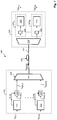
- Fig. 6 shows an optical WDM transmission system 200 comprising a plurality of N optical transmitter devices 102 i (1 ⁇ i ⁇ N) forming a WDM transmitter device 202 and a corresponding plurality of N receiver devices 102 i (1 ⁇ i ⁇ N) forming a WDM receiver device 204.
- Each of the optical transmitter devices 102 i reveals a design according to the single channel transmission system shown in Fig. 5 . The same applies to the receiver devices 102 i .
- the N optical transmitter devices 102 i are connected to dedicated channel ports of a multiplexer device 206, which combines the optical binary digital transmit signals SMH TX,I created by the optical transmitter devices 102 i to an optical WDM transmission signal.
- the optical WDM transmission signal S WDM is supplied to the transmission link 106 and transmitted to the far end of the transmission link 106, which is connected to a demultiplexer device 208.
- each of the optical transmitters 114 emits at two center wavelengths (two different modes), wherein the selected one of each of these two modes differs in its center frequency from the center frequency of the selected mode of a respective neighboring channel.
- the optical transmitters 114 may be realized as or may comprise identical widely tunable semiconductor lasers, which are controlled to emit at two modes depending on a dedicated binary digital modulation signal S mod,i .
- the multiplexer device 206 may be realized by a simple 1xN optical coupler.
- each of the optical bandpass filters 118 has a bandwidth and a center wavelength, i.e. a passband, according to a predetermined definition of the channels of the WDM transmission system 200.
- Fig. 7 shows a further embodiment of a WDM transmission system 300 similar to the embodiment according to Fig. 6 .
- the optical transmitter device 302 of the embodiment according to Fig. 7 comprises a filter device 316 which combines the functionality of filtering the modulated optical output signals S opt,i in order to create corresponding optical binary digital transmit signals SMH TX,I and to combine these signals to an optical WDM transmission signal S WDM .
- This optical filter device 316 may be realized by an arrayed waveguide grating (AWG) 318.
- AWG arrayed waveguide grating
- the multiplexers in the form of AWGs are widely used in order to define the channel passbands, these AWGs may simultaneously be used in order to effect the desired bandpass filtering of the modulated optical output signals S opt,i created by the optical transmitters 114. That is, in order to realize the method and transmission system according to the present invention, no additional optical filter means are required.
- the mode hopping effect is essentially caused or influenced by two parameters, which also depend on the gain current I gain , namely the temperature and the charge carrier density in the active region of the semiconductor laser 3. Both parameters influence the phase.
- the "charge carrier effect” is dominant for higher bit rates, e.g. for bit rates above 4 to 6 Gbit/s depending on the design of the semiconductor laser.
- the "temperature effect” is dominant in for lower bit rates, e.g below 4 to 6 Gb/s.
- an electrical high-pass filter 17 may be provided at the input port of the semiconductor laser 3.
- all or selected ones of the optical transmitters 114 in the systems 100, 200 and 300 as shown in Figs. 5 , 6 and 7 may comprise an electrical high-pass filter at the respective input ports of the semiconductor lasers comprised by the optical transmitters 114.
- the high-pass filter 17 enables a steep increase or decrease of the gain current I gain at the transitions in the binary digital modulation signal S mod .
- the high-pass filter 17 may be realized as a simple RC high-pass filter, comprising a resistance R which is connected parallel to a capacitance C.
Landscapes
- Engineering & Computer Science (AREA)
- Computer Networks & Wireless Communication (AREA)
- Signal Processing (AREA)
- Physics & Mathematics (AREA)
- Electromagnetism (AREA)
- Optics & Photonics (AREA)
- Optical Communication System (AREA)
Claims (13)
- Verfahren zum Erzeugen eines optischen binären digitalen Übertragungssignals, das einer optischen Übertragungsstrecke, insbesondere einer optischen Wellenlängenmultiplex(WDM)-Übertragungsstrecke, zugeführt werden soll, umfassend die folgenden Schritte:(a) Betreiben eines optischen Senders (114) in einem solchen Zustand, dass ein Modensprung zwischen einem vordefinierten ersten und einem vordefinierten zweiten optischen Modus des optischen Senders (114) auftritt, wenn ein binäres digitales Modulationssignal (Smod) dem optischen Sender (114) zugeführt wird,(b) Erzeugen eines modulierten optischen Ausgangssignals (Sopt) des optischen Senders (114), das dem binären digitalen Modulationssignal (Smod) entspricht, das dem optischen Sender (114) zugeführt wird, wobei ein erster Zustand des binären digitalen Modulationssignals (Smod) zu einem modulierten optischen Ausgangssignal (Sopt) bei einer Mittenwellenlänge des ersten optischen Modus führt und ein zweiter Zustand des binären digitalen Modulationssignals zu einem modulierten optischen Ausgangssignal (Sopt) bei einer Mittenwellenlänge des zweiten optischen Modus führt,gekennzeichnet durch den folgenden weiteren Schritt:(c) optisches Filtern des modulierten optischen Ausgangssignals (Sopt) auf eine solche Weise, dass zumindest ein Teil des optischen Leistungsspektrums des modulierten optischen Ausgangssignals (Sopt), das durch einen ausgewählten des ersten und zweiten optischen Modus verursacht wird, unterdrückt oder zumindest abgeschwächt wird,(d) Ausgeben des optisch gefilterten modulierten Signals an die Übertragungsstrecke.
- Verfahren nach Anspruch 1, dadurch gekennzeichnet, dass der optische Modus, der einen niedrigeren Peak in dem optischen Leistungsspektrum verursacht, ausgewählt ist, um das optische Filtern des modulierten optischen Ausgangssignals (Sopt) zu bewirken.
- Verfahren nach einem der vorhergehenden Ansprüche, dadurch gekennzeichnet, dass für das optische Filtern des modulierten optischen Ausgangssignals (Sopt) eine optische Filtervorrichtung (116; 216; 316) verwendet wird, die eine Kanalbandbreite der optischen Übertragungsstrecke (106) definiert, die dem optischen binären digitalen Übertragungssignal (SMHTX) zugewiesen ist.
- Verfahren nach Anspruch 3, dadurch gekennzeichnet, dass die optische Filtervorrichtung (316) ein Wellenlängenmultiplexermittel ist, das angepasst ist, um eine Vielzahl von modulierten optischen Ausgangssignalen (Sopt) optisch zu filtern und zu multiplexen.
- Verfahren nach einem der vorhergehenden Ansprüche, dadurch gekennzeichnet, dass das binäre digitale Modulationssignal (Smod) elektrisch hochpassgefiltert wird, bevor es einem abstimmbaren Halbleiterlaser (3) zugeführt wird, den der optische Sender (114) umfasst.
- Optische Sendevorrichtung zum Erzeugen mindestens eines optischen binären digitalen Übertragungssignals, das einer optischen Übertragungsstrecke, insbesondere einer optischen Wellenlängenmultiplex-Übertragungsstrecke, zugeführt werden soll, umfassend:(a) mindestens einen optischen Sender (114), der konfiguriert ist, um in einem Modensprungzustand betrieben zu werden oder konfiguriert ist, um steuerbar zu sein, um darin betrieben zu werden, wobei ein Modensprung zwischen einem vordefinierten ersten und einem vordefinierten zweiten optischen Modus des optischen Senders (114) in Abhängigkeit von einem ersten und einem zweiten Zustand eines binären digitalen Modulationssignal (Smod) auftritt, das dem mindestens einen optischen Sender (114) zugeführt wird, und(b) eine Steuervorrichtung (112), die ein dediziertes binäres digitales Modulationssignal (Smod) jedem des mindestens einen optischen Senders (114) zuführt,(c) wobei jedes des mindestens einen optischen Senders (114) und der Steuervorrichtung (112) konfiguriert ist, um ein moduliertes optisches Ausgangssignal (Sopt) zu erzeugen, das dem binären digitalen Modulationssignal (Smod) entspricht, wobei ein erster Zustand des binären digitalen Modulationssignals (Smod) zu einem modulierten optischen Ausgangssignal (Sopt) bei einer Mittenwellenlänge des ersten optischen Modus führt und ein zweiter Zustand des binären digitalen Modulationssignals (Smod) zu einem modulierten optischen Ausgangssignal (Sopt) bei einer Mittenwellenlänge des zweiten optischen Modus führt,
dadurch gekennzeichnet, dass(d) die optische Sendevorrichtung (102) ferner eine optische Filtervorrichtung (116; 216; 316) umfasst, die konfiguriert ist, um jedes des mindestens einen modulierten optischen Ausgangssignals (Sopt) so optisch zu filtern, dass zumindest ein Teil des optischen Leistungsspektrums des modulierten optischen Ausgangssignals (Sopt), das durch einen ausgewählten des ersten und zweiten optischen Modus verursacht wird, unterdrückt oder zumindest abgeschwächt wird. - Optische Sendevorrichtung nach Anspruch 6, dadurch gekennzeichnet, dass die Steuervorrichtung (112) konfiguriert ist, um mindestens ein Zustandssteuersignal (SCTR; 11, 13) dem mindestens einen optischen Sender (114) zuzuführen, wobei das mindestens eine Steuersignal (SCTR; 11, 13) den mindestens einen optischen Sender (114) steuert, um in dem Modensprungzustand betrieben zu werden.
- Optische Sendevorrichtung nach Anspruch 7, dadurch gekennzeichnet, dass der mindestens eine optische Sender (114) ein abstimmbarer optischer Sender ist und dass die Steuervorrichtung (112) konfiguriert ist, um mindestens ein Zustandssteuersignal (SCTR; 11, 13) dem mindestens einen optischen Sender (114) zuzuführen, wobei das mindestens eine Zustandssteuersignal (SCTR; 11, 13) den mindestens einen optischen Sender steuert, um in einem vordefinierten Modensprungzustand betrieben zu werden, wobei ein Modensprung zwischen einem vordefinierten ersten und einem vordefinierten zweiten optischen Modus mit einer ersten bzw. einer zweiten Mittenwellenlänge auftritt.
- Optische Sendevorrichtung nach Anspruch 8, dadurch gekennzeichnet, dass der abstimmbare optische Sender (114) einen abstimmbaren Halbleiterlaser (3), vorzugsweise einen Halbleiterlaser mit einer Struktur mit mehreren Sektionen umfasst.
- Optische Sendevorrichtung nach einem der Ansprüche 6 bis 9, dadurch gekennzeichnet,(a) dass sie eine Vielzahl von optischen Sendern (114) umfasst,(b) dass die optische Filtervorrichtung (116; 216) einen separaten optischen Filter (118) für jeden des mindestens einen optischen Senders (114) umfasst, wobei jeder optische Sender (114) und jeder dedizierte optische Filter (118) konfiguriert sind, um ein optisches binäres digitales Übertragungssignal bei einer vorgegebenen Mittenwellenlänge zu erzeugen, und(c) dass die optischen binären digitalen Übertragungssignale (SMHTX) einer optischen Multiplexer-Vorrichtung (206) zugeführt werden, die konfiguriert ist, um die optischen binären digitalen Übertragungssignale (SMHTX) mit einem optischen WDM-Signal (SWDM) zu kombinieren.
- Optische Sendevorrichtung nach einem der Ansprüche 6 bis 9, dadurch gekennzeichnet,(a) dass sie eine Vielzahl von optischen Sendern (114) umfasst und(b) dass die optische Filtervorrichtung (316) als eine optische Multiplexer- und Filtervorrichtung (318) umgesetzt wird, die konfiguriert ist, um ein optisches WDM-Signal (SWDM) zu erzeugen, indem die modulierten optischen Ausgangssignale (Sopt) gefiltert und kombiniert werden, die von den optischen Sendern (114) erzeugt und der optischen Filtervorrichtung (316) zugeführt werden.
- Optische Sendevorrichtung nach Anspruch 11, dadurch gekennzeichnet, dass die optische Filtervorrichtung (316) durch ein Arrayed-Waveguide Grating (318) oder durch eine andere Vorrichtung umgesetzt wird, welche die Funktionalität eines Arrayed-Waveguide Grating aufweist.
- Optische Sendevorrichtung nach einem der Ansprüche 7 bis 12, dadurch gekennzeichnet, dass der mindestens eine optische Sender (114) einen elektrischen Hochpassfilter umfasst, der konfiguriert ist, um ein elektrisches Hochpassfiltern des binären digitalen Modulationssignals (Smod) durchzuführen, bevor es dem abstimmbaren Halbleiterlaser (3) zugeführt wird.
Priority Applications (2)
| Application Number | Priority Date | Filing Date | Title |
|---|---|---|---|
| EP16187142.1A EP3291464B1 (de) | 2016-09-02 | 2016-09-02 | Verfahren und vorrichtung zum optischen senden zur erzeugung eines optischen binären digitalen sendesignals |
| US15/685,141 US10355784B2 (en) | 2016-09-02 | 2017-08-24 | Method and optical transmitter device for creating an optical binary digital transmit signal |
Applications Claiming Priority (1)
| Application Number | Priority Date | Filing Date | Title |
|---|---|---|---|
| EP16187142.1A EP3291464B1 (de) | 2016-09-02 | 2016-09-02 | Verfahren und vorrichtung zum optischen senden zur erzeugung eines optischen binären digitalen sendesignals |
Publications (2)
| Publication Number | Publication Date |
|---|---|
| EP3291464A1 EP3291464A1 (de) | 2018-03-07 |
| EP3291464B1 true EP3291464B1 (de) | 2021-04-07 |
Family
ID=56853555
Family Applications (1)
| Application Number | Title | Priority Date | Filing Date |
|---|---|---|---|
| EP16187142.1A Active EP3291464B1 (de) | 2016-09-02 | 2016-09-02 | Verfahren und vorrichtung zum optischen senden zur erzeugung eines optischen binären digitalen sendesignals |
Country Status (2)
| Country | Link |
|---|---|
| US (1) | US10355784B2 (de) |
| EP (1) | EP3291464B1 (de) |
Family Cites Families (13)
| Publication number | Priority date | Publication date | Assignee | Title |
|---|---|---|---|---|
| FR2668670B1 (fr) | 1990-10-31 | 1992-12-31 | France Etat | Procede de transmission optique par decalage en longueur d'onde et systeme correspondant. |
| JP3302310B2 (ja) * | 1997-12-11 | 2002-07-15 | ケイディーディーアイ株式会社 | 光増幅伝送システム及び光増幅装置 |
| US6738536B2 (en) * | 2001-12-20 | 2004-05-18 | Optinel Systems, Inc. | Wavelength tunable filter device for fiber optic systems |
| US7092641B2 (en) * | 2002-05-31 | 2006-08-15 | Avago Technologies Fiber Ip (Singapore) Pte. Ltd. | Method and apparatus for optical transmission of wavelength-encoded modulation formats |
| US7558488B2 (en) * | 2002-11-06 | 2009-07-07 | Finisar Corporation | Reach extension by using external Bragg grating for spectral filtering |
| KR100658338B1 (ko) * | 2004-04-09 | 2006-12-14 | 노베라옵틱스코리아 주식회사 | 다단 분기 광 분배망을 갖는 파장 분할 다중 방식 수동형광 네트워크 |
| US20060239609A1 (en) * | 2005-04-26 | 2006-10-26 | Sorin Wayne V | Methods and apparatuses to increase wavelength channels in a wavelength-division-multiplexing passive-optical-network |
| JP2008083449A (ja) * | 2006-09-28 | 2008-04-10 | Sumitomo Osaka Cement Co Ltd | 進行波型光変調器 |
| KR100975881B1 (ko) * | 2007-12-21 | 2010-08-13 | 한국전자통신연구원 | 외부 씨드 광원을 이용한 파장 분할 다중화 수동형광가입자망(wdm-pon) |
| KR20100092853A (ko) * | 2009-02-13 | 2010-08-23 | 한국과학기술원 | 저잡음 다파장 광원을 구비한 저잡음 광신호의 전송 장치, 저잡음 다파장 광원을 이용한 방송 신호 전송 장치, 및 이를 구비한 광가입자망 |
| US8565618B2 (en) * | 2010-10-05 | 2013-10-22 | Verizon Patent And Licensing Inc. | Automatic wavelength configuration |
| US8818208B2 (en) * | 2011-07-14 | 2014-08-26 | Applied Optoelectronics, Inc. | Laser mux assembly for providing a selected wavelength |
| US9329659B2 (en) * | 2013-02-06 | 2016-05-03 | Veris Industries, Llc | Power monitoring system that determines frequency and phase relationships |
-
2016
- 2016-09-02 EP EP16187142.1A patent/EP3291464B1/de active Active
-
2017
- 2017-08-24 US US15/685,141 patent/US10355784B2/en active Active
Non-Patent Citations (1)
| Title |
|---|
| None * |
Also Published As
| Publication number | Publication date |
|---|---|
| US20180069635A1 (en) | 2018-03-08 |
| US10355784B2 (en) | 2019-07-16 |
| EP3291464A1 (de) | 2018-03-07 |
Similar Documents
| Publication | Publication Date | Title |
|---|---|---|
| US8073342B2 (en) | Method and apparatus for transmitting optical signals | |
| US6766116B2 (en) | Optical transmission system | |
| KR0157429B1 (ko) | 파장분할 다중화 광통신 시스템의 송신장치 및 광신호 시스템 | |
| US20040208428A1 (en) | Wavelength-multiplexed narrow-bandwidth optical transmitter and wavelength-multiplexed vestigial-side-band optical transmitter | |
| US8331786B2 (en) | Transmission method of WDM light and WDM optical transmission system | |
| US20020154372A1 (en) | Power and optical frequency monitoring system and transmission system of frequency-modulated optical signal | |
| US9523867B2 (en) | Off quadrature biasing of Mach Zehnder modulator for improved OSNR performance | |
| US6763197B1 (en) | Optical transmitter and optical transmitter control method using variable duty ratio setting and alternate phase inversion for optical clock pulses | |
| US10225016B1 (en) | Optical power and chromatic dispersion equalization system | |
| CA2619307C (en) | Optical transmitting apparatus and temperature controlling method used therefor | |
| WO2001071959A2 (en) | Method and system of transmitting optical signals generated by multi-line sources via wdm optical network | |
| US10263722B2 (en) | Multi-wavelength balanced optical transmission networks | |
| JP4935279B2 (ja) | Osnr測定装置およびosnr測定方法 | |
| EP1376902B1 (de) | Optischer Restseitenbandsender/-empfänger | |
| EP1424795B1 (de) | Optisches Übertragungssystem unter Verwendung eines optischen Phasenmodulators | |
| EP3291464B1 (de) | Verfahren und vorrichtung zum optischen senden zur erzeugung eines optischen binären digitalen sendesignals | |
| JP3782402B2 (ja) | 光送信装置および光通信システム | |
| EP1241804B1 (de) | Quelle für optische Pulse für optische Fernübertragunssysteme | |
| US20030185573A1 (en) | Optical transmission systems | |
| US20030152387A1 (en) | Method for transmitting multi-level signals through dispersive media | |
| US7486851B2 (en) | Tunable single-channel dispersion compensator for high-speed optical systems | |
| US20050041983A1 (en) | Method of forming a coded optical signal with a return to zero or non return to zero format | |
| JP2005094287A (ja) | 光伝送方法及びシステム並びに光送信方法及び装置 | |
| JP2579559B2 (ja) | 光波長フィルタ装置 | |
| US20070166039A1 (en) | Integrated optical transmitter |
Legal Events
| Date | Code | Title | Description |
|---|---|---|---|
| PUAI | Public reference made under article 153(3) epc to a published international application that has entered the european phase |
Free format text: ORIGINAL CODE: 0009012 |
|
| STAA | Information on the status of an ep patent application or granted ep patent |
Free format text: STATUS: THE APPLICATION HAS BEEN PUBLISHED |
|
| AK | Designated contracting states |
Kind code of ref document: A1 Designated state(s): AL AT BE BG CH CY CZ DE DK EE ES FI FR GB GR HR HU IE IS IT LI LT LU LV MC MK MT NL NO PL PT RO RS SE SI SK SM TR |
|
| AX | Request for extension of the european patent |
Extension state: BA ME |
|
| STAA | Information on the status of an ep patent application or granted ep patent |
Free format text: STATUS: REQUEST FOR EXAMINATION WAS MADE |
|
| 17P | Request for examination filed |
Effective date: 20180824 |
|
| RBV | Designated contracting states (corrected) |
Designated state(s): AL AT BE BG CH CY CZ DE DK EE ES FI FR GB GR HR HU IE IS IT LI LT LU LV MC MK MT NL NO PL PT RO RS SE SI SK SM TR |
|
| GRAP | Despatch of communication of intention to grant a patent |
Free format text: ORIGINAL CODE: EPIDOSNIGR1 |
|
| STAA | Information on the status of an ep patent application or granted ep patent |
Free format text: STATUS: GRANT OF PATENT IS INTENDED |
|
| INTG | Intention to grant announced |
Effective date: 20201104 |
|
| GRAS | Grant fee paid |
Free format text: ORIGINAL CODE: EPIDOSNIGR3 |
|
| GRAA | (expected) grant |
Free format text: ORIGINAL CODE: 0009210 |
|
| STAA | Information on the status of an ep patent application or granted ep patent |
Free format text: STATUS: THE PATENT HAS BEEN GRANTED |
|
| AK | Designated contracting states |
Kind code of ref document: B1 Designated state(s): AL AT BE BG CH CY CZ DE DK EE ES FI FR GB GR HR HU IE IS IT LI LT LU LV MC MK MT NL NO PL PT RO RS SE SI SK SM TR |
|
| REG | Reference to a national code |
Ref country code: GB Ref legal event code: FG4D |
|
| REG | Reference to a national code |
Ref country code: AT Ref legal event code: REF Ref document number: 1381039 Country of ref document: AT Kind code of ref document: T Effective date: 20210415 Ref country code: CH Ref legal event code: EP |
|
| REG | Reference to a national code |
Ref country code: DE Ref legal event code: R096 Ref document number: 602016055549 Country of ref document: DE |
|
| REG | Reference to a national code |
Ref country code: IE Ref legal event code: FG4D |
|
| REG | Reference to a national code |
Ref country code: LT Ref legal event code: MG9D |
|
| REG | Reference to a national code |
Ref country code: NL Ref legal event code: MP Effective date: 20210407 Ref country code: AT Ref legal event code: MK05 Ref document number: 1381039 Country of ref document: AT Kind code of ref document: T Effective date: 20210407 |
|
| PG25 | Lapsed in a contracting state [announced via postgrant information from national office to epo] |
Ref country code: BG Free format text: LAPSE BECAUSE OF FAILURE TO SUBMIT A TRANSLATION OF THE DESCRIPTION OR TO PAY THE FEE WITHIN THE PRESCRIBED TIME-LIMIT Effective date: 20210707 Ref country code: AT Free format text: LAPSE BECAUSE OF FAILURE TO SUBMIT A TRANSLATION OF THE DESCRIPTION OR TO PAY THE FEE WITHIN THE PRESCRIBED TIME-LIMIT Effective date: 20210407 Ref country code: HR Free format text: LAPSE BECAUSE OF FAILURE TO SUBMIT A TRANSLATION OF THE DESCRIPTION OR TO PAY THE FEE WITHIN THE PRESCRIBED TIME-LIMIT Effective date: 20210407 Ref country code: FI Free format text: LAPSE BECAUSE OF FAILURE TO SUBMIT A TRANSLATION OF THE DESCRIPTION OR TO PAY THE FEE WITHIN THE PRESCRIBED TIME-LIMIT Effective date: 20210407 Ref country code: NL Free format text: LAPSE BECAUSE OF FAILURE TO SUBMIT A TRANSLATION OF THE DESCRIPTION OR TO PAY THE FEE WITHIN THE PRESCRIBED TIME-LIMIT Effective date: 20210407 Ref country code: LT Free format text: LAPSE BECAUSE OF FAILURE TO SUBMIT A TRANSLATION OF THE DESCRIPTION OR TO PAY THE FEE WITHIN THE PRESCRIBED TIME-LIMIT Effective date: 20210407 |
|
| PG25 | Lapsed in a contracting state [announced via postgrant information from national office to epo] |
Ref country code: PL Free format text: LAPSE BECAUSE OF FAILURE TO SUBMIT A TRANSLATION OF THE DESCRIPTION OR TO PAY THE FEE WITHIN THE PRESCRIBED TIME-LIMIT Effective date: 20210407 Ref country code: NO Free format text: LAPSE BECAUSE OF FAILURE TO SUBMIT A TRANSLATION OF THE DESCRIPTION OR TO PAY THE FEE WITHIN THE PRESCRIBED TIME-LIMIT Effective date: 20210707 Ref country code: PT Free format text: LAPSE BECAUSE OF FAILURE TO SUBMIT A TRANSLATION OF THE DESCRIPTION OR TO PAY THE FEE WITHIN THE PRESCRIBED TIME-LIMIT Effective date: 20210809 Ref country code: RS Free format text: LAPSE BECAUSE OF FAILURE TO SUBMIT A TRANSLATION OF THE DESCRIPTION OR TO PAY THE FEE WITHIN THE PRESCRIBED TIME-LIMIT Effective date: 20210407 Ref country code: SE Free format text: LAPSE BECAUSE OF FAILURE TO SUBMIT A TRANSLATION OF THE DESCRIPTION OR TO PAY THE FEE WITHIN THE PRESCRIBED TIME-LIMIT Effective date: 20210407 Ref country code: IS Free format text: LAPSE BECAUSE OF FAILURE TO SUBMIT A TRANSLATION OF THE DESCRIPTION OR TO PAY THE FEE WITHIN THE PRESCRIBED TIME-LIMIT Effective date: 20210807 Ref country code: GR Free format text: LAPSE BECAUSE OF FAILURE TO SUBMIT A TRANSLATION OF THE DESCRIPTION OR TO PAY THE FEE WITHIN THE PRESCRIBED TIME-LIMIT Effective date: 20210708 Ref country code: LV Free format text: LAPSE BECAUSE OF FAILURE TO SUBMIT A TRANSLATION OF THE DESCRIPTION OR TO PAY THE FEE WITHIN THE PRESCRIBED TIME-LIMIT Effective date: 20210407 |
|
| REG | Reference to a national code |
Ref country code: DE Ref legal event code: R097 Ref document number: 602016055549 Country of ref document: DE |
|
| PG25 | Lapsed in a contracting state [announced via postgrant information from national office to epo] |
Ref country code: ES Free format text: LAPSE BECAUSE OF FAILURE TO SUBMIT A TRANSLATION OF THE DESCRIPTION OR TO PAY THE FEE WITHIN THE PRESCRIBED TIME-LIMIT Effective date: 20210407 Ref country code: RO Free format text: LAPSE BECAUSE OF FAILURE TO SUBMIT A TRANSLATION OF THE DESCRIPTION OR TO PAY THE FEE WITHIN THE PRESCRIBED TIME-LIMIT Effective date: 20210407 Ref country code: SK Free format text: LAPSE BECAUSE OF FAILURE TO SUBMIT A TRANSLATION OF THE DESCRIPTION OR TO PAY THE FEE WITHIN THE PRESCRIBED TIME-LIMIT Effective date: 20210407 Ref country code: SM Free format text: LAPSE BECAUSE OF FAILURE TO SUBMIT A TRANSLATION OF THE DESCRIPTION OR TO PAY THE FEE WITHIN THE PRESCRIBED TIME-LIMIT Effective date: 20210407 Ref country code: CZ Free format text: LAPSE BECAUSE OF FAILURE TO SUBMIT A TRANSLATION OF THE DESCRIPTION OR TO PAY THE FEE WITHIN THE PRESCRIBED TIME-LIMIT Effective date: 20210407 Ref country code: EE Free format text: LAPSE BECAUSE OF FAILURE TO SUBMIT A TRANSLATION OF THE DESCRIPTION OR TO PAY THE FEE WITHIN THE PRESCRIBED TIME-LIMIT Effective date: 20210407 Ref country code: DK Free format text: LAPSE BECAUSE OF FAILURE TO SUBMIT A TRANSLATION OF THE DESCRIPTION OR TO PAY THE FEE WITHIN THE PRESCRIBED TIME-LIMIT Effective date: 20210407 |
|
| PLBE | No opposition filed within time limit |
Free format text: ORIGINAL CODE: 0009261 |
|
| STAA | Information on the status of an ep patent application or granted ep patent |
Free format text: STATUS: NO OPPOSITION FILED WITHIN TIME LIMIT |
|
| 26N | No opposition filed |
Effective date: 20220110 |
|
| REG | Reference to a national code |
Ref country code: CH Ref legal event code: PL |
|
| REG | Reference to a national code |
Ref country code: BE Ref legal event code: MM Effective date: 20210930 |
|
| PG25 | Lapsed in a contracting state [announced via postgrant information from national office to epo] |
Ref country code: IS Free format text: LAPSE BECAUSE OF FAILURE TO SUBMIT A TRANSLATION OF THE DESCRIPTION OR TO PAY THE FEE WITHIN THE PRESCRIBED TIME-LIMIT Effective date: 20210807 Ref country code: MC Free format text: LAPSE BECAUSE OF FAILURE TO SUBMIT A TRANSLATION OF THE DESCRIPTION OR TO PAY THE FEE WITHIN THE PRESCRIBED TIME-LIMIT Effective date: 20210407 Ref country code: AL Free format text: LAPSE BECAUSE OF FAILURE TO SUBMIT A TRANSLATION OF THE DESCRIPTION OR TO PAY THE FEE WITHIN THE PRESCRIBED TIME-LIMIT Effective date: 20210407 |
|
| PG25 | Lapsed in a contracting state [announced via postgrant information from national office to epo] |
Ref country code: LU Free format text: LAPSE BECAUSE OF NON-PAYMENT OF DUE FEES Effective date: 20210902 Ref country code: IT Free format text: LAPSE BECAUSE OF FAILURE TO SUBMIT A TRANSLATION OF THE DESCRIPTION OR TO PAY THE FEE WITHIN THE PRESCRIBED TIME-LIMIT Effective date: 20210407 Ref country code: IE Free format text: LAPSE BECAUSE OF NON-PAYMENT OF DUE FEES Effective date: 20210902 Ref country code: FR Free format text: LAPSE BECAUSE OF NON-PAYMENT OF DUE FEES Effective date: 20210930 Ref country code: BE Free format text: LAPSE BECAUSE OF NON-PAYMENT OF DUE FEES Effective date: 20210930 |
|
| PG25 | Lapsed in a contracting state [announced via postgrant information from national office to epo] |
Ref country code: LI Free format text: LAPSE BECAUSE OF NON-PAYMENT OF DUE FEES Effective date: 20210930 Ref country code: CH Free format text: LAPSE BECAUSE OF NON-PAYMENT OF DUE FEES Effective date: 20210930 |
|
| PG25 | Lapsed in a contracting state [announced via postgrant information from national office to epo] |
Ref country code: HU Free format text: LAPSE BECAUSE OF FAILURE TO SUBMIT A TRANSLATION OF THE DESCRIPTION OR TO PAY THE FEE WITHIN THE PRESCRIBED TIME-LIMIT; INVALID AB INITIO Effective date: 20160902 |
|
| PG25 | Lapsed in a contracting state [announced via postgrant information from national office to epo] |
Ref country code: CY Free format text: LAPSE BECAUSE OF FAILURE TO SUBMIT A TRANSLATION OF THE DESCRIPTION OR TO PAY THE FEE WITHIN THE PRESCRIBED TIME-LIMIT Effective date: 20210407 |
|
| P01 | Opt-out of the competence of the unified patent court (upc) registered |
Effective date: 20230630 |
|
| PG25 | Lapsed in a contracting state [announced via postgrant information from national office to epo] |
Ref country code: MK Free format text: LAPSE BECAUSE OF FAILURE TO SUBMIT A TRANSLATION OF THE DESCRIPTION OR TO PAY THE FEE WITHIN THE PRESCRIBED TIME-LIMIT Effective date: 20210407 |
|
| PG25 | Lapsed in a contracting state [announced via postgrant information from national office to epo] |
Ref country code: TR Free format text: LAPSE BECAUSE OF FAILURE TO SUBMIT A TRANSLATION OF THE DESCRIPTION OR TO PAY THE FEE WITHIN THE PRESCRIBED TIME-LIMIT Effective date: 20210407 |
|
| REG | Reference to a national code |
Ref country code: DE Ref legal event code: R081 Ref document number: 602016055549 Country of ref document: DE Owner name: ADTRAN NETWORKS SE, DE Free format text: FORMER OWNER: ADVA OPTICAL NETWORKING SE, 98617 MEININGEN, DE |
|
| PG25 | Lapsed in a contracting state [announced via postgrant information from national office to epo] |
Ref country code: MT Free format text: LAPSE BECAUSE OF FAILURE TO SUBMIT A TRANSLATION OF THE DESCRIPTION OR TO PAY THE FEE WITHIN THE PRESCRIBED TIME-LIMIT Effective date: 20210407 |
|
| PGFP | Annual fee paid to national office [announced via postgrant information from national office to epo] |
Ref country code: DE Payment date: 20250919 Year of fee payment: 10 |
|
| PGFP | Annual fee paid to national office [announced via postgrant information from national office to epo] |
Ref country code: GB Payment date: 20250923 Year of fee payment: 10 |