EP3292508B1 - Transducteur ultrasonore piézoélectrique micro-usiné (pmut) intégré (pmut) sur circuit intégré (ic) pour détection d'empreintes digitales - Google Patents
Transducteur ultrasonore piézoélectrique micro-usiné (pmut) intégré (pmut) sur circuit intégré (ic) pour détection d'empreintes digitales Download PDFInfo
- Publication number
- EP3292508B1 EP3292508B1 EP15767646.1A EP15767646A EP3292508B1 EP 3292508 B1 EP3292508 B1 EP 3292508B1 EP 15767646 A EP15767646 A EP 15767646A EP 3292508 B1 EP3292508 B1 EP 3292508B1
- Authority
- EP
- European Patent Office
- Prior art keywords
- exemplary
- layer
- pmut
- mems
- array
- Prior art date
- Legal status (The legal status is an assumption and is not a legal conclusion. Google has not performed a legal analysis and makes no representation as to the accuracy of the status listed.)
- Active
Links
Images




















Classifications
-
- H—ELECTRICITY
- H03—ELECTRONIC CIRCUITRY
- H03H—IMPEDANCE NETWORKS, e.g. RESONANT CIRCUITS; RESONATORS
- H03H3/00—Apparatus or processes specially adapted for the manufacture of impedance networks, resonating circuits, resonators
- H03H3/007—Apparatus or processes specially adapted for the manufacture of impedance networks, resonating circuits, resonators for the manufacture of electromechanical resonators or networks
- H03H3/0072—Apparatus or processes specially adapted for the manufacture of impedance networks, resonating circuits, resonators for the manufacture of electromechanical resonators or networks of microelectro-mechanical resonators or networks
- H03H3/0073—Integration with other electronic structures
-
- G—PHYSICS
- G06—COMPUTING OR CALCULATING; COUNTING
- G06V—IMAGE OR VIDEO RECOGNITION OR UNDERSTANDING
- G06V40/00—Recognition of biometric, human-related or animal-related patterns in image or video data
- G06V40/10—Human or animal bodies, e.g. vehicle occupants or pedestrians; Body parts, e.g. hands
- G06V40/12—Fingerprints or palmprints
- G06V40/13—Sensors therefor
- G06V40/1306—Sensors therefor non-optical, e.g. ultrasonic or capacitive sensing
Definitions
- the subject disclosure relates to microelectromechanical (MEMS) devices, to piezoelectric MEMS devices for fingerprint sensing, and more particularly to integrated piezoelectric MEMS transducers (PMUTs) on integrated circuit (IC) for fingerprint sensing.
- MEMS microelectromechanical
- PMUTs integrated piezoelectric MEMS transducers
- Microelectromechanical systems enable integration of both microelectronic circuits and mechanical structures on a single chip or device, thereby significantly lowering fabrication costs and/or chip size.
- MEMS ultrasound transducers can have applications not possible in conventional bulk piezoelectric devices, e.g., medical imaging, such as intravascular guiding and diagnosis, fingerprint detection, etc.
- traditional manufacturing methods are ineffective in creating area array interconnection and reduced transducer sizes.
- MUT devices as an alternative method for fingerprint detection typically require MUT devices to be manufactured in the resolution of at least 300 dots per inch (dpi) or higher e.g., approximately 85 micrometer ( ⁇ m) pixel size.
- dpi dots per inch
- CMUT capacitive MUT
- CMUT linear arrays are subject to skin condition and sensor contamination, which can deteriorate the accuracy of fingerprint detection devices employing CMUT linear arrays.
- EP 1 533 743 A1 relates to a fingerprint sensor and a fabrication method thereof.
- the fingerprint sensor includes: a complementary metal-oxide semiconductor structure which is formed on a substrate that is doped with a first type dopant; an insulating layer which is formed on the complementary metal-oxide semiconductor structure; a lower electrode which is formed in a central portion of the insulating layer; a piezoelectric region which is formed on the lower electrode; an upper electrode which is formed on the piezoelectric layer; and a fingerprint contact layer which is formed to cover a portion of an upper surface of the insulating layer on which the lower electrode has not been formed, the lower electrode, the piezoelectric region, and the upper electrode.
- the MEMS device comprises a MEMS wafer including a handle wafer with one or more cavities containing a first surface and a second surface and an insulating layer deposited on the second surface of the handle wafer.
- the MEMS device also includes a device layer having a third and fourth surface, the third surface bonded to the insulating layer of the second surface of handle wafer; and a metal conductive layer on the fourth surface.
- the MEMS device also includes CMOS wafer bonded to the MEMS wafer.
- the CMOS wafer includes at least one metal electrode, such that an electrical connection is formed between the at least one metal electrode and at least a portion of the metal conductive layer.
- an exemplary MEMS device can comprise a MEMS ultrasound transducer (MUT) structure and a piezoelectric material disposed within the MEMS device comprising a piezoelectric MUT (PMUT) array of a fingerprint sensor adapted to sense a characteristic of a fingerprint placed adjacent to the MUT structure.
- An exemplary MEMS device can further comprise a first metal conductive layer disposed on the piezoelectric material and a plurality of metal electrodes configured to form electrical connections between the first metal conductive layer, the piezoelectric material, and a complementary metal oxide semiconductor (CMOS) structure, wherein the pMUT structure and the CMOS structure are vertically stacked.
- CMOS complementary metal oxide semiconductor
- an exemplary MEMS device can comprise a CMOS device wafer associated with an integrated PMUT array of a fingerprint sensor and having a plurality of cavities configured in an array.
- An exemplary MEMS device can further comprise a first metal conductive layer disposed on the CMOS device wafer and over the plurality of cavities, a piezoelectric material disposed on the first metal conductive layer, and a second metal conductive layer, disposed on the piezoelectric material, electrically coupling the second metal conductive layer and at least one CMOS device wafer electrode, and electrically coupling the first metal conductive layer to at least one other CMOS device wafer electrode, wherein the plurality of cavities, the piezoelectric material, the first metal conductive layer, and the second metal conductive layer are configured as a plurality of PMUT structures.
- exemplary methods are described directed to PMUTs suitable for integration with CMOS integrated circuits (ICs), as well as PMUT arrays having high fill factor for fingerprint sensing.
- MEMS microelectromechanical systems
- MEMS devices include but are not limited to gyroscopes, accelerometers, magnetometers, pressure sensors, and radio-frequency components. Silicon wafers containing MEMS structures are referred to as MEMS wafers.
- MEMS device may refer to a semiconductor device implemented as a microelectromechanical system.
- MEMS structure may refer to any feature that may be part of a larger MEMS device.
- An engineered silicon-on-insulator (ESOI) wafer may refer to a SOI wafer with cavities beneath the silicon device layer or substrate.
- Handle wafer typically refers to a thicker substrate used as a carrier for the thinner silicon device substrate in a silicon-on-insulator wafer. Handle substrate and handle wafer can be interchanged.
- a cavity may refer to an opening or recession in a substrate wafer and enclosure may refer to a fully enclosed space.
- Bond chamber may be an enclosure in a piece of bonding equipment where the wafer bonding process takes place. The atmosphere in the bond chamber determines the atmosphere sealed in the bonded wafers.
- a system and method in accordance with the present invention describes a class of RF MEMS devices, sensors, and actuators including but not limited to switches, resonators and tunable capacitors that are hermetically sealed and bonded to integrated circuits that may use capacitive sensing and electrostatic, magnetic, or piezoelectric actuation.
- FIG. 1A illustrates a cross-section view of a MEMS structure 100 in accordance with a first example, not forming part of the present invention.
- FIG. 1A shows a MEMS structure with addition of metal on the silicon structural layer.
- the structure includes a CMOS wafer 102 bonded to a MEMS wafer 104.
- the MEMS wafer 104 comprises a silicon device layer 106 fusion bonded to a handle wafer 108 through an oxide layer 109.
- a MEMS aluminum 110 metal layer is added to the silicon device layer 106.
- CMOS wafer 102 and MEMS wafer 104 are connected through the silicon stand-offs 112 using an aluminum-germanium eutectic bond formed by germanium 111 and aluminum 113. Apart from the stand-offs 112 the bulk of the current is carried by the metal layers 117.
- spacers 114 composed of an insulating material such as Silicon Oxide or Silicon Nitride may be placed on bottom metal layer 117 to reduce stiction and control the gap between the top metal layer 110 and the bottom metal layer 117.
- FIG. 1B illustrates a cross-section view of a MEMS structure 100' in accordance with a second embodiment.
- FIG. 1B shows a MEMS structure with additional insulating layer 112a deposited onto the MEMS aluminum 110 and insulating layer 112b deposited onto the bottom electrode 117 to prevent shorting and create a well-defined capacitive gap when the movable MEMS structure consisting of the silicon device layer 106, MEMS aluminum 110, and insulating layer 112a are brought into contact with the electrodes on the CMOS wafer 102.
- FIG. 2 illustrates a cross-section view of a MEMS structure 200 in accordance with a third embodiment.
- FIG. 2 shows a MEMS structure similar to FIG. 1A .
- the electrical connection between the CMOS wafer 102' and the MEMS wafer 104' occurs through physical contact between the CMOS aluminum 204 on the CMOS wafer 102' and the MEMS aluminum 110' on the MEMS wafer 104' connected by an Aluminum-Germanium layer created by the eutectic reaction between germanium 206 and CMOS aluminum 113' on the CMOS wafer 102' and the MEMS aluminum 110' on the MEMS wafer 104'.
- One possible risk of this embodiment is a preferential reaction of the germanium 206 with the MEMS aluminum 110' (since that is the layer it is directly deposited on) with a possibly insufficient reaction with the CMOS aluminum 113'.
- the insufficient reaction may lead to poor bonds and marginal electrical connections.
- FIG. 3 illustrates a cross-section view of a MEMS structure 300 in accordance with a fourth embodiment.
- FIG. 3 shows a MEMS structure identical to FIG. 2 with the exception of a barrier layer 302 deposited between the MEMS aluminum 110" and germanium 206'.
- the barrier layer 302 is electrically conductive and makes an electrical contact with aluminum upon physical contact.
- the objective of the barrier layer 302 is to prevent a eutectic reaction between the MEMS aluminum 110" and germanium 206', leaving germanium 206'to eutectically react with the CMOS aluminum 113".
- One such barrier layer may be Titanium Nitride.
- the CMOS aluminum 113" will mix with germanium 206' creating an electrical contact and physical bond to the barrier layer 302 on the MEMS aluminum 110", thereby creating an electrical contact between the CMOS wafer 102" and MEMS wafer 104".
- FIG. 4 illustrates a cross-section view of a MEMS structure 400 in accordance with a fifth embodiment.
- FIG. 4 shows a MEMS structure identical to FIG. 3 , but with an insulating layer 402 deposited between the MEMS aluminum 110'" and silicon device layer 106'" thereby electrically insulating the silicon from the metal.
- the insulating layer 402 is needed in cases where it is not desirable to carry any electrical signal in the silicon layer (for example in RF applications where signal transmission in the silicon would produce a power loss).
- the MEMS aluminum 110'" is still capacitively coupled to the silicon device layer 106'" through the insulating layer 402.
- the insulating layer must be sufficiently thick to minimize capacitance or the silicon must be sufficiently resistive so as to minimize electrical signal coupling into it.
- FIG. 5 is a flowchart of a process for adding metal and piezoelectric layers to a MEMS structure.
- the process starts with an Engineered SOI 502.
- a first metal layer (metal 1) is deposited onto the device silicon surface via step 504 followed by the piezoelectric layer deposition (e.g ., Aluminum Nitride or PZT) pattern and etch via step 506.
- a second metal layer (Metal 2) deposited onto the wafer to serve as a top electrode for the piezoelectric layer as well as to provide electrical contact between Metal 1 and the CMOS substrate via step 508.
- a germanium layer is deposited onto Metal 1 and patterned to define germanium pads in regions where bonding to CMOS will take place via step 510.
- the MEMS wafer is bonded to a CMOS wafer such that germanium pads eutectically react with aluminum pads on the CMOS creating electrical and physical contact between the CMOS aluminum and MEMS Metal 2 via step 512.
- FIG. 6 illustrates a cross-section view of a MEMS structure 600 in accordance with a sixth embodiment that utilizes a piezoelectric layer.
- a piezoelectric layer 602 enables a range of applications including acoustic resonators and filters and piezo-actuated devices.
- the piezoelectric layer 602 typically requires a bottom electrode 604 and top electrodes 606.
- the bottom electrode 604 may comprise a first metal layer (metal 1) (Ex. Aluminium, Ruhtenium, Tungsten, Molybdenum or Platinum).
- a silicon device layer can be used as a bottom electrode 604.
- the top electrode 606 and interconnect 610 are composed of a second metal layer (metal 2) (Ex. Aluminum).
- the top electrode 606 and interconnect 610 make physical and electrical contact to the CMOS aluminum pads 608 using an Aluminum Germanium bond.
- the bottom electrode 604 may make physical and electrical contact to the interconnect 610 thereby connecting to the CMOS wafer. Electrical potentials may be applied between top electrodes 606 and the bottom electrode 604 or between individual top electrodes 606. These potentials create electric fields to induce strains within the piezoelectric material.
- FIG. 7 illustrates a cross-section view of a MEMS structure 700 in accordance with a seventh embodiment.
- FIG. 7 shows the same structure as in FIG. 6 with an addition of a silicon dioxide layer 702 between the device layer silicon 106 and metal layer, 604".
- the silicon dioxide layer, 702 serves as a temperature stabilization layer that improves frequency stability of the resonator or filter over temperature by offsetting the positive Young's modulus temperature coefficient of silicon with the negative Young's modulus temperature coefficient of silicon oxide.
- FIG. 8 illustrates a cross-section view of a MEMS structure 800 in accordance with a eighth embodiment.
- FIG. 8 shows the same structure as in FIG. 7 with an addition of a patterned bottom electrode 604".
- a patterned bottom electrode 604" By patterning the bottom electrode 604", multiple potentials may be applied to different sections of the bottom surface of the piezoelectric material 602, leading to more design flexibility and potentially more efficient devices.
- the ability to input electrical signals on both the bottom and top of the piezoelectric structure can lead to higher coupling efficiency.
- the subject application provides disclosure of a microelectromechanical system (MEMS) integration flow to incorporate aluminum nitride (AlN) on an engineering substrate and a top electrode layer combined with aluminum germanium (AlGe) with complementary metal-oxide-semiconductor (CMOS) wafers/layers/substrates.
- MEMS microelectromechanical system
- the subject application further describes a MEMS integration flow that comprises starting wafers/layers/substrates (e.g., complementary metal-oxide-semiconductor (CMOS) wafers/layers/substrates, MEMS handle wafers/layers/substrates, and/or MEMS device wafers/layers/substrates) and a plurality of masking layers, for example, ten masking layers, though, as will be appreciated by those of ordinary skill, a fewer or a greater number of masking layers can be utilized without unduly departing from the generality and scope of the subject disclosure.
- CMOS complementary metal-oxide-semiconductor
- the MEMS handle wafers/layers/substrates can be patterned with back-side alignment mark layers used for front-to-back alignment after fusion bonding. Cavities that define suspended MEMS structures can also be etched in a front-side of the MEMS handle wafers/layers/substrates. The MEMS handle layers/wafers/substrates can then be oxidized and fusion-bonded to MEMS device layers/wafers/substrates.
- the MEMS device layers/wafers/substrates can, for example, comprise silicon (Si) structural layers that can be ground and polished to target thicknesses, at which point aluminum nitride seed layers can be disposed over a surface of the silicon structural layers, molybdenum layers can be deposited over the aluminum nitride seed layers, aluminum nitride stacking layers can be deposited over the molybdenum layers, and/or silicon dioxide standoff layers can be disposed on the aluminum nitride stacking layers.
- Si silicon
- the silicon dioxide standoff layers can be etched on the MEMS device layers/wafers/substrates to provide separations between the MEMS structures and the complementary metal-oxide-semiconductor wafers/layers/substrates.
- the aluminum nitride (AlN) stacking layers can then be patterned through a silicon dioxide hard mask with structures, bottom contacts, and/or aluminum nitride top contact masks. Additionally, aluminum, titanium, and germanium can then be deposited in sequence from bottom to top and patterned with germanium pads and electrodes.
- the silicon device layer can then be patterned and etched using, for instance an anisotropic etch process used to create deep penetration, steep-sided holes and trenches in layers/wafers/substrates, typically with high aspect ratios, such as deep reactive-ion etching (DRIE), to define release structures.
- DRIE deep reactive-ion etching
- the combination of the structures and release layers that define the fully released structure are formed on the upper cavity.
- a bottom cavity can be etched in the complementary metal-oxide-semiconductor layer/wafer to allow clearance for out-of-plane moving of the MEMS structures (e.g ., combinations of silicon and aluminum nitride stacking layers) or damping control.
- the MEMS and complementary metal-oxide-semiconductor wafers/layers/substrates can then be bonded using aluminum-germanium (Al-Ge) eutectic bonding to create hermetic seals around the MEMS structures as well as electrical interconnects between the MEMS structures and complementary metal-oxide-semiconductor circuits.
- the bonded wafer/layer can be thinned on the MEMS side to a desired thickness and a port can be formed on the polished side of the MEMS wafer/layer to create access to the surrounding environment. Silicon tabs on the MEMS wafer/layer can thereafter be removed using, for example, a dicing process to expose the complementary metal-oxide-semiconductor wire-bond pads.
- the MEMS 900 can comprise a handle wafer/layer/substrate 904 that can have been patterned with back-side alignment mark layers to be employed for front-to-back alignment after fusion bonding. Further, a front side of handle wafer/layer/substrate 904 can have been etched to form cavities 902. As depicted handle wafer/layer/substrate 904 can be formed of a silicon layer/substrate into which cavities 902 can have been etched.
- a silicon dioxide layer/substrate 906 can be deposited on the silicon layer/substrate 904 thereby overlaying silicon layer/substrate 904 and cavities 902 formed therein. Disposed and/or deposited over silicon dioxide layer/substrate 906 and fusion bonded to the silicon dioxide layer/substrate 906 can be a substrate/layer formed of silicon 908.
- the handle wafer/layer/substrate 904 inclusive of formed cavities 902 and silicon dioxide layer 906 can be referred to as an engineered substrate, and for purposes of this disclosure can be referred to a the MEMS handle layer.
- silicon dioxide layer/substrate 906 (silicon layer/substrate 904 inclusive of etched cavities 902 and silicon dioxide layer/substrate 906 can form and be referred to as the MEMS handle layer/wafer/substrate), and a substrate/layer 908 formed of silicon
- silicon dioxide standoffs 916 can be formed on the MEMS handle layer/wafer/substrate by, for example, successively depositing aluminum nitride seed layers 910, molybdenum layers 912, and aluminum nitride stacking layers 914 over silicon substrate/layer 908, prior to etching and/or forming silicon dioxide standoffs 916.
- the additional deposited or disposed layers comprising the aluminum nitride seed layers 910, molybdenum layers 912, aluminum nitride stacking layers 914, and silicon dioxide standoffs 916 over silicon substrate/layer 908 can be referred to the MEMS device layer/wafer/substrate and/or piezoelectric layer/wafer/substrate.
- Silicon substrate layer 908 can be the silicon structural layer of the MEMS device layer to which the MEMS handle layer (e.g., silicon layer/substrate 904 inclusive of etched cavities 902 and silicon dioxide layer/substrate 906) can have been fusion bonded to the MEMS device layer/wafer/substrate (e.g., silicon structural substrate/layer 908, aluminum nitride seed layers 910, molybdenum layers 912, aluminum nitride stacking layers 914, and standoffs 916).
- the MEMS handle layer e.g., silicon layer/substrate 904 inclusive of etched cavities 902 and silicon dioxide layer/substrate 906
- the MEMS device layer/wafer/substrate e.g., silicon structural substrate/layer 908, aluminum nitride seed layers 910, molybdenum layers 912, aluminum nitride stacking layers 914, and standoffs 916.
- the MEMS handle layer prior to fusion bonding of the MEMS handle layer to the MEMS device layer, can typically have been oxidized and the silicon structural layer/substrate 908 of the MEMS device layer can have been ground and polished to a target or defined thickness prior to deposition of the aluminum nitride seed layers 910, molybdenum layers 912, aluminum nitride stacking layers 914, and standoffs 916 formed of silicon dioxide. Standoffs 916 are typically formed on the MEMS device layer to provide separation between the MEMS structure and a CMOS wafer/layer/substrate.
- FIGS. 9C-9E provide illustration of a further cross-sectional view of MEMS device 900 including the layers described above in connection with FIGS. 9A-9B .
- structure can be defined and separate bottom electrodes 920 can be carved out by first disposing or depositing a silicon dioxide hard mask 918 over the aluminum nitride stacking layers 914 and standoffs 916 and thereafter etching through silicon dioxide hard mask 918 to define the structure and carve out separate bottom electrodes 920.
- the etching process etches through layers/substrates respectively formed of silicon dioxide hard mask 918, aluminum nitride 914, molybdenum 912, and aluminum nitride seed layer 910, to the silicon structural layer/substrate 908.
- a bottom electrodes contact 922 can be created.
- a opening etch on silicon dioxide layer 918 can be performed to define aluminum nitride top contacts 924 and avoids unnecessary HBAR resonance from the pad. Defining the structure and carving out the bottom electrodes 920, creating bottom electrode contacts 922, and defining aluminum nitride top contacts 924, as depicted in FIGS. 9C-9E , can be undertaken by patterning the aluminum nitride stacking layers through silicon dioxide hard mark 918.
- FIG. 9F aluminum and titanium layers 926 are deposited for the purposes of top electrode material deposition and then germanium layers 928 are deposited over the aluminum and titanium layers 926 so that germanium pads 928 and electrodes 930 can be patterned as depicted in FIGS. 9G-H .
- the device layer can be overlaid with a layer of photo-resist 932 and patterned and etched using deep reactive-ion etching (DRIE) to define release structures, as depicted in FIG. 9I . Only the combination of the structure and release layer can define the fully released structure 934 (See FIG. 9J ) in the cavity 902.
- DRIE deep reactive-ion etching
- a cavity 938 is etched into a CMOS wafer 936 to allow clearance for out-of-plane moving MEMS structures 934 and/or damping control, and thereafter the CMOS wafer 936 and MEMS device wafer 940 are bonded using an Aluminum-Germanium eutectic bond to create a hermetic seal around MEMS structure 934 and CMOS circuits and form a bonded wafer 942.
- the eutectically bonded wafer 942 can then be thinned, for instance, on the MEMS wafer side, to a defined or desired thickness and a port 944 can be formed on a polished side of the MEMS wafer 942 to create access to the surrounding environment, as illustrated in FIG. 9K .
- silicon tabs on the MEMS wafer 942 can be removed using a dicing process to expose CMOS wire bond pads.
- a partial silicon etch can be performed wherein structural silicon layer 908 (e.g., the structural silicon layer of the MEMS device wafer) can partially be further etched 1002.
- the partial etch 1002 can be performed to partially thin down the silicon device layer (e.g ., structural silicon layer 908).
- the partial etch 1002 can be accomplished with a structure layer mask through silicon etch or silicon deep reactive-ion etching.
- partial etch 1002 can be an additional etch to that previously performed to define structure and carve out separate bottom electrodes 920 as elucidated above in connection with FIG. 9C . Additionally and/or alternatively, partial etch 1002 and the etch performed to define structure and carve out separate bottom electrodes 920, as depicted in FIG. 9C , can be accomplished in a single act without unduly and/or unnecessarily departing from the intent and generality of the subject disclosure.
- an additional act of can be performed subsequent to etching port 944 on a polished side of the MEMS wafer 942 (see e.g., FIG. 9K ).
- an infra-red (IR) absorption layer 1102 can be deposited on the back of the MEMS handle wafer 940.
- the infra-red (IR) absorption layer 1102, as illustrated, can be disposed not only on the back of the MEMS handle wafer 940 but also in the previously etched port 944.
- standoff 916 formations techniques can be employed.
- a layer of silicon 908 can be deposited over the MEMS handle layer/wafer/substrate (e.g., silicon layer/wafer/substrate 904 inclusive of cavities 902 and silicon dioxide layer/substrate 906) and thereafter the deposited layer of silicon 908 can be partially etched to form standoffs 916, thus, referring back to FIG. 9A and as illustrated in FIG. 12(a)(i), standoffs 916 can have been formed from the structural silicon layer 908 of the MEMS device layer or piezoelectric layer/wafer/substrate.
- structural silicon layer 908 can be overlaid with a silicon dioxide layer and thereafter the deposited silicon dioxide layer can be patterned to create or form standoffs 916, as illustrated in FIG. 12(a)(ii).
- deposition of piezoelectric stacking layers 1202, as described and illustrated in connection with FIGS. 9C-9K can be carried out as respectively depicted in FIGS. 12(b)(i) and 12(b)(ii).
- FIGS. 12(b)(i) it will be observed that the subsequent piezoelectric stacking layers 1202, as described in relation to FIGS. 9C-9K , overlay silicon standoffs 916, whereas, in connection with FIG. 12(b)(ii), the successive layers that comprise the piezoelectric stacking layers 1202, as disclosed with respect to FIGS. 9C-9K , are deposited over silicon dioxide standoffs 916.
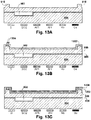
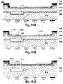
- FIG. 13 illustrates an additional and/or alternative process flow than that described and disclosed in connection with FIGS. 9A-9K .
- silicon standoffs 916 can have been formed by patterning and/or partially etching structural silicon layer 908.
- the piezoelectric layer stacking e.g ., aluminum nitride seed layers 910, molybdenum layer 912, and aluminum nitride stacking layer 914 described earlier with respect to FIG.
- FIG. 9B can be reduced to only an aluminum nitride layer 1302, wherein an aluminum nitride layer 1302 is overlaid and patterned 1304 on top of the structural silicon layer 908 inclusive of the formed silicon standoffs 916.
- the structural silicon layer 908 inclusive of the silicon standoffs 916 can be used as bottom electrodes.
- the aluminum nitride layer 1302 can be overlaid with aluminum and titanium layers 1306.
- patterning in aluminum nitride layer 1302 at 1304 will be filled by the aluminum and titanium layers 1306.
- germanium pads 1308 can be defined, wherein a germanium layer can be overlaid aluminum and titanium layers 1306 to form the germanium pads 1308. Further, in FIG. 13E the previously deposited aluminum and titanium layers 1306 can be selectively patterned to define aluminum and titanium pads 1310 and to expose the underlying aluminum nitride layer 1302. In FIG. 13F a silicon dioxide hard mask 1312 can be deposited over defined germanium pads 1308, aluminum and titanium pads 1310, and exposed aluminum nitride layer 1302 and an etch or patterning performed to define the structure 1314.
- a CMOS wafer 936 can be eutectically bonded to the MEMS device wafer 1316, in a manner similar to that described in the context of FIG. 9J and illustrated in FIG. 13G . Further, on completion of the eutectic bonding of the CMOS wafer 936 to the MEMS device wafer 1316, a port 1318 can be formed on a polished side or surface of the MEMS device wafer 1316, as illustrated in FIG. 13H .
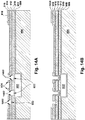
- a silicon dioxide layer 1404 can be deposited to overlay the layers previously described in the context of FIG. 9E . It will be observed on examination of FIG. 14B that the silicon dioxide layer 1404 has been disposed to cover the sidewalls 1402 as well as bottom electrodes 920 and the bottom electrodes contact 922. Additionally, as will also have been observed on inspection of FIG.
- the deposited silicon dioxide layer 1404 will also have covered the aluminum nitride top contact 924.
- the deposition and patterning of silicon dioxide layer 1404 provides isolation Once the silicon dioxide layer 1404 has been deposited as illustrated in FIG. 14B , the silicon dioxide layer 1404 can undergo a blank reactive-ion etch to create sidewall protection 1406.
- a MEMS device comprising: a first silicon substrate comprising: a handle layer comprising a first surface and a second surface, the second surface comprises a cavity; an insulating layer deposited over the second surface of the handle layer; a device layer having a third surface bonded to the insulating layer and a fourth surface; a piezoelectric layer deposited over the fourth surface of the device layer; a metal conductivity layer disposed over the piezoelectric layer; a bond layer disposed over a portion of the metal conductivity layer; and a stand-off formed on the first silicon substrate; wherein the first silicon substrate is bonded to a second silicon substrate, comprising: a metal electrode configured to form an electrical connection between the metal conductivity layer formed on the first silicon substrate and the second silicon substrate.
- the stand-off can be formed on the piezoelectric layer and can be formed as a silicon layer or as a silicon dioxide layer deposited on the device layer. Additionally and/or alternatively, the stand-off can be formed of silicon dioxide deposited on the piezoelectric layer.
- the piezoelectric layer can be patterned and etched to form a sidewall in the piezoelectric layer, wherein a first dielectric layer can be interposed between the piezoelectric layer and the metal conductive layer, and a second dielectric layer can be disposed on the sidewall of the piezoelectric layer.
- a first dielectric layer can be interposed between the piezoelectric layer and the metal conductive layer
- a second dielectric layer can be disposed on the sidewall of the piezoelectric layer.
- an opening in the handle layer can be exploited to expose the device layer
- an orifice in the device layer can be used to expose the piezoelectric layer
- the device layer can include an aperture.
- the device layer can be selectively or partially removed
- the piezoelectric layer can in an embodiment comprise aluminum nitride or in another embodiment can comprise: an aluminum nitride (AlN) seed layer, a bottom metal layer, and an aluminum nitride (AlN) layer.
- AlN aluminum nitride
- AlN aluminum nitride
- an infra-red (IR) absorption layer can be deposited on a portion of the device layer and/or the infra-red (IR) absorption layer can be deposited on a portion of the piezoelectric layer.
- a method is described and disclosed.
- the method can comprise a sequence of machine executable operations that can include depositing an insulation layer over a handle layer that comprises a first surface and a second surface, wherein the second surface comprises a cavity and the insulation layer is formed on the second surface of the handle layer; bonding a first surface of a device layer to the insulation layer; depositing a piezoelectric layer on a second surface of the device layer; depositing a metal conductivity layer over the piezoelectric layer; partially depositing a bond layer over the metal conductivity layer; forming a stand-off on the second surface of the device layer; and establishing an electrical connection between the metal conductivity layer and a silicon substrate.
- Further machine executable method operations can include: depositing a silicon layer or a silicon dioxide layer to form the stand-off; depositing a silicon dioxide layer to form a stand-off positioned on the piezoelectric layer; patterning and etching of the piezoelectric layer to form a sidewall; interposing a first dielectric layer between the piezoelectric layer and the metal conductive layer; disposing a second dielectric layer on the sidewall of the piezoelectric layer; exposing the device layer via a first opening in the handle layer; and exposing the piezoelectric layer through the first opening and a second opening in the device layer.
- Additional machine executed method acts can also include: selectively removing a portion of the device layer; depositing an infra-red (IR) absorption layer on a selected portion of the device layer; and depositing an infra-red (IR) absorption layer on a selected portion of the piezoelectric layer.
- IR infra-red
- a microelectromechanical device that can comprise: a first silicon substrate bonded to a second silicon substrate, comprising: an electrode on the second silicon substrate that electrically contacts a conductivity layer disposed on the first silicon substrate; the conductivity layer on the first silicon substrate is disposed over a piezoelectric layer on the first silicon substrate; the piezoelectric layer on the first silicon substrate is deposited over a device layer that comprises a stand-off formed on the first silicon substrate; and the device layer on the first silicon substrate is bonded to an dielectric layer that is deposited over a surface of a handle layer on the first silicon substrate that comprises a cavity.
- the subject application further describes MEMS devices and fingerprint sensing.
- finger print sensors There are two kinds of finger print sensors, namely swipe-based and area-based.
- optical method is too bulky and expensive; thermal and swipe-based RF method are not the favored due to user experience; area-based ultrasound and RF sensors have challenges to lower the manufacturing cost.
- area-based ultrasound and RF sensors have challenges to lower the manufacturing cost.
- above conventional fingerprint sensor technologies are subject to errors due to finger contamination, sensor contamination, imaging errors, etc.
- Various embodiments disclosed herein provide for improved fingerprint sensor performance by measuring a frequency response of a piezoelectric acoustic resonator.
- a device can include an array of piezoelectric transducers, and an array of cavities that has been attached to the array of piezoelectric transducers to form an array of resonators, e.g ., an array of MEMS piezoelectric acoustic resonators.
- a resonator e.g., a membrane resonator, a Helmholtz resonator, etc. of the array of resonators can be associated with a first frequency response, e.g., a resonant frequency of the resonator, a Q factor of the resonator, etc. corresponding to a determination that the resonator has a non-touch baseline condition.
- a second frequency response e.g ., increase in resonant frequency of the resonator, decrease in Q factor of the resonator, etc. corresponding to a determination that the resonator has been touched, e.g., by the finger ridge.
- the finger print map can be determined according to the frequency response changes of resonators in the resonator array.
- the array of piezoelectric transducers can include a piezoelectric material; a first set of electrodes that has been formed a first side of the piezoelectric material; and a second set of electrodes that has been formed on second side of the piezoelectric material - a piezoelectric transducer of the array of piezoelectric transducers corresponding to the resonator including a first electrode of the first set of electrodes and a second electrode of the second set of electrodes.
- the piezoelectric transducer comprises a portion of the resonator, e.g., a membrane resonator, that has been touched.
- a first end of a cavity of array of cavities corresponding to a portion of the resonator, e.g., a Helmholtz resonator, that has been touched is smaller than a second end of the cavity.
- the first end of the cavity is open to the environment, e.g., air adjacent to the device, etc.
- the cavity has been filled with a first material corresponding to a first acoustic velocity that is different from a second acoustic velocity corresponding to a second material that is adjacent to, surrounding, etc. the cavity.
- Another embodiment can include a system, e.g., a piezoelectric acoustic resonator based fingerprint sensor, etc. that can include an array of piezoelectric transducers; an array of cavities that has been attached to the array of piezoelectric transducers to form an array of resonators; a memory to store instructions; and a processor coupled to the memory, that facilitates execution of the instructions to perform operations, comprising: determining a frequency response of a resonator of the array of resonators - the resonator including a piezoelectric transducer of the array of piezoelectric transducers and a cavity of the array of cavities; and determining that the resonator has been touched, e.g., by a finger, etc. in response determining that a change in the frequency response satisfies a defined condition, e.g., a resonant frequency of the resonator has increased, a Q factor of the resonator has decreased, etc.
- a first portion of the cavity e.g ., corresponding to a portion of the resonator that has been touched, is smaller than a second portion of the cavity.
- the first portion of the cavity is open to the environment.
- the cavity has been filled with a first material corresponding to a first acoustic velocity that is different from a second acoustic velocity corresponding to a second material that is adjacent to the cavity.
- One embodiment can include a method including forming an array of piezoelectric transducers on a first substrate; forming one or more portions of an array of cavities using a second substrate; and attaching the array of piezoelectric transducers to the second substrate to form an array of resonators.
- a resonator e.g., a membrane resonator, a Helmholtz resonator, etc. of the array of resonators can be associated with a first frequency response with respect to, e.g., a resonant frequency of the resonator, a Q factor of the resonator, etc. corresponding to a determined non-touch of the resonator.
- the resonator can be associated with a second frequency response with respect to, e.g., the resonant frequency, the Q factor, etc. corresponding to a determined touch of the resonator.
- the method can include removing the first substrate from the array of piezoelectric transducers.
- the forming of the array of piezoelectric transducers can include forming a first set of electrodes on a first side of a piezoelectric material, and forming a second set of electrodes on a second side of the piezoelectric material - a piezoelectric transducer of the array of piezoelectric transducers corresponding to the resonator can include a first electrode of the first set of electrodes and a second electrode of the second set of electrodes.
- the method can include filling a cavity of the array of cavities corresponding to the resonator, e.g ., the Helmholtz resonator, with a material having a first acoustic velocity that is different from a second acoustic velocity of the second substrate.
- the resonator e.g ., the Helmholtz resonator
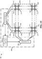
- Piezoelectric acoustic resonator based sensor 1500 includes control component 1502 and array of piezoelectric acoustic resonators 1505.
- Control component 1502 e.g., a system, an application specific integrated circuit (ASIC), etc. can include computing device(s), memory device(s), computing system(s), logic, etc.
- a frequency response e.g., a change in a resonant frequency, a change in a Q factor, etc. of a piezoelectric acoustic resonator (1510, 1605 (see below), 2005 (see below), etc. ) of array of piezoelectric acoustic resonators 1505.
- processing component 1504 can determine, based on the frequency response, whether the piezoelectric acoustic resonator has been touched, e.g., by a ridge of a finger, and further derive a fingerprint based on determining which piezoelectric acoustic resonator(s) 1510 of array of piezoelectric acoustic resonators 1505 have been touched.
- FIG. 16 illustrates a block diagram of a cross section of MEMS piezoelectric acoustic resonator 1605, in accordance with various embodiments.
- MEMS piezoelectric acoustic resonator 1605 e.g., a Helmholtz resonator
- cavity 1640 includes an opening that is exposed to the environment, e.g ., air.
- MEMS piezoelectric acoustic resonator 1605 includes piezoelectric transducer 1607, which includes top electrode 1610, piezoelectric material 1620, e.g., piezoelectric membrane, polyvinylidene fluoride (PVDF), etc. and bottom electrode 1630.
- top electrode 1610 and bottom electrode 1630 can be manufactured from a conductive material, e.g ., metal, and control component 1502 can generate and apply a stimulus, e.g ., a pulse signal, a frequency sweep, an alternating current (AC) voltage, an AC current, etc. to piezoelectric transducer 1607 via top electrode 1610 and bottom electrode 1630.
- a stimulus e.g ., a pulse signal, a frequency sweep, an alternating current (AC) voltage, an AC current, etc.
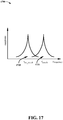
- control component 1502 can measure, e.g., utilizing a network analyzer, etc. based on the stimulus, e.g., based on a Fourier transform analysis, resonant frequency 1710, e.g., corresponding to a non-touch of piezoelectric acoustic resonator 1605, and resonant frequency 320, e.g., corresponding to a touch of piezoelectric acoustic resonator 1605.
- resonant frequency 1710 e.g., corresponding to a non-touch of piezoelectric acoustic resonator 1605
- resonant frequency 320 e.g., corresponding to a touch of piezoelectric acoustic resonator 1605.
- control component 1502 in response to determining that the resonant frequency of piezoelectric acoustic resonator 1605 has increased, e.g., to resonant frequency 1720, control component 1502 can determine that MEMS piezoelectric acoustic resonator 1605 has been touched, e.g., by a ridge of a finger.
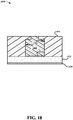
- FIG. 18 illustrates a block diagram of a cross section a MEMS piezoelectric acoustic resonator including material 1810, in accordance with various embodiments.
- cavity 1640 can be filled with material 1810, e.g., rubber, gel, etc. that is associated with a first acoustic velocity that is different from a second acoustic velocity corresponding to substrate 1650.
- a resonant frequency of MEMS piezoelectric acoustic resonator 1605 can be modified in a predetermined manner by selecting material 1810 of a predetermined acoustic velocity with respect to an acoustic velocity of substrate 1650.
- including material 1810 in cavity 1640 can prevent debris, contaminants, etc. from entering cavity 1640 and subsequently introducing errors in measurements of the resonant frequency of MEMS piezoelectric acoustic resonator 1605.
- FIG. 19 illustrates a block diagram of a cross section of a portion of an array (1920) of MEMS piezoelectric acoustic resonators (1605) being contacted by finger 1910, in accordance with various embodiments.
- Control component 1502 can determine that finger ridge 1932 has touched a MEMS piezoelectric acoustic resonator (1605) of the portion of the array based on a determination that a resonant frequency of the MEMS piezoelectric acoustic resonator has increased.
- control component 1502 can determine that other MEMS piezoelectric acoustic resonators (1605) of the portion of the array have not been touched, e.g., by finger ridge 1930 and finger ridge 1934, based on respective determinations that resonant frequencies of the other MEMS piezoelectric acoustic resonators has not changed. In this regard, control component 1502 can derive, based on such determinations, a fingerprint corresponding to finger 510.
- MEMS piezoelectric acoustic resonator 2005 e.g., a membrane resonator
- cavity 2010 that has been formed by, within, etc. substrate 1650, e.g., a silicon based material, and has been enclosed by bottom electrode 1630 of piezoelectric transducer 1607.
- Control component 1502 can generate and apply a stimulus, e.g ., a pulse signal, a frequency sweep, an alternating AC voltage, an AC current, etc. to piezoelectric transducer 1607 via top electrode 1610 and bottom electrode 1630.
- a stimulus e.g ., a pulse signal, a frequency sweep, an alternating AC voltage, an AC current, etc.
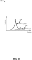
- control component 1502 can measure, based on the stimulus, Q factor 2110, e.g., corresponding to a non-touch of piezoelectric acoustic resonator 2005, and Q factor 2120, e.g., corresponding to a touch of piezoelectric acoustic resonator 2005.
- Q factor 2110 e.g., corresponding to a non-touch of piezoelectric acoustic resonator 2005
- Q factor 2120 e.g., corresponding to a touch of piezoelectric acoustic resonator 2005.
- control component 1502 in response to determining that the Q factor of piezoelectric acoustic resonator 2005 has decreased, e.g., to Q factor 2120, control component 1502 can determine that MEMS piezoelectric acoustic resonator 2005 has been touched, e.g., by a ridge of a finger.
- FIG. 22 illustrates a block diagram of a cross section of a portion of an array (2220) of MEMS piezoelectric acoustic resonators (2005) being contacted by finger 1910, in accordance with various embodiments.
- Control component 1502 can determine that finger ridge 1932 has touched a MEMS piezoelectric acoustic resonator (2005) of the portion of the array based on a determination that a Q factor of the MEMS piezoelectric acoustic resonator has decreased.
- control component 1502 can determine that other MEMS piezoelectric acoustic resonators (2005) of the portion of the array have not been touched, e.g., by finger ridge 1930 and finger ridge 1934, based on respective determinations that Q factors of the other MEMS piezoelectric acoustic resonators have not changed. In this regard, control component 1502 can derive, based on such determinations, a fingerprint corresponding to finger 1910.
- top electrode 1610 can form a square shape that can be smaller, and located above, a square shape of bottom electrode 1630.
- top electrode 1610 can form a shape of a regular polygon that can be smaller, and located above, a regular polygon shape of bottom electrode 1630.
- FIG. 29 provides further shapes and configurations of exemplary PMUT arrays having high fill factor, in accordance with further non-limiting embodiments.
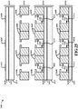
- FIG. 25 a block diagram (2500) representing a method for manufacturing, assembling, etc. a MEMS piezoelectric acoustic resonator, e.g., MEMS piezoelectric acoustic resonator 1605, is illustrated, in accordance with various embodiments.
- an array of piezoelectric transducers (1607) can be formed on substrate 2510.
- bottom electrodes (1630) can be formed on substrate 2510; dielectric material 1620 can be formed on, placed on, etc. the bottom electrodes; and top electrodes (1610) can be formed on, placed on, etc. dielectric material 1620.
- portions(s) of an array of cavities (1640) can be formed on substrate 1650.
- the portion(s) of the array of cavities can be placed on, attached to, etc. the array of piezoelectric transducers (1607).
- one or more cavities of the array of cavities can be filled with a material having a first acoustic velocity that is different from a second acoustic velocity of substrate 1650.
- substrate 2510 can be removed from the bottom electrodes.
- FIG. 26 illustrates a block diagram (2600) representing another method for manufacturing, assembling, etc.
- a MEMS piezoelectric acoustic resonator e.g., MEMS piezoelectric acoustic resonator 2005
- an array of piezoelectric transducers (1607) can be formed on substrate 2610.
- top electrodes can be formed on substrate 2610; dielectric material 1620 can be formed on, placed on, etc. the top electrodes and substrate 2610; and bottom electrodes (2630) can be formed on, placed on, etc. dielectric material 1620.
- portions(s) of an array of cavities (2010) can be formed on substrate 1650.
- the portion(s) of the array of cavities can be placed on, attached to, etc. the array of piezoelectric transducers (1607).
- substrate 2610 can be removed from dielectric material 1620 and the top electrodes.
- the subject application further describes PMUTs for fingerprint sensing.
- MUT devices as an alternative method for fingerprint detection typically require MUT devices to be manufactured in the resolution of at least 300 dpi or higher e.g ., approximately 85 ⁇ m pixel size.
- optical method can be too bulky or expensive; thermal and capacitive sensing swipe-based method are not the favored due to user experience.
- area-based fingerprint sensor is convenient in usage, it is suitable for adoption in mobile devices and can provide a sufficient level of security.
- ultrasonic fingerprint detection can overcome deficiencies associated with skin condition and/or sensor contamination that afflict the accuracy of fingerprint detection devices employing CMUT linear arrays.
- existing fingerprint sensors are mostly based on capacitive sensing. Their detection ability is readily compromised by excessively dry or wet fingerprints and/or contamination from sweat or oil. Ultrasonic detection does not rely on electrical property, instead, it relies on physical contact and acoustic impedance difference and is proven to be able to detect ridges and valleys and also sweat pores which are not so easily detectable with capacitive sensing.
- Various embodiments disclosed herein provide integrated PMUTs on IC for fingerprint sensing. Additionally, various embodiments can provide an efficient way of creating electrical coupling and mechanical anchoring of ultrasonic transducer pMUT directly on CMOS for reduced parasitics and fully utilize the routing capability on CMOS metal layers.
- a high fill factor for a PMUT array that can provide a desired output pressure for the ultrasound transducer array.
- Various embodiments described herein can thus increase the increase the signal to noise ratio (SNR) of PMUT arrays during detection and the array gain, which is the ratio of the array's output pressure to that of a single PMUT device.
- SNR signal to noise ratio
- increasing fill factor can suppress mechanical coupling between adjacent PMUT pixels.
- various embodiments disclosed herein provide integrated PMUTs on IC for fingerprint sensing where the PMUT structures and the array of PMUT structures are configured in a rhombus configuration, a hexagonal configuration, and/or a combination of rhombus configuration and hexagonal configuration.
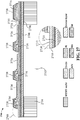
- FIG. 27 depicts a cross-section of an exemplary PMUT 2700 for fingerprint sensing, in accordance with various embodiments.
- exemplary PMUT 2700 can comprise an engineered silicon-on-insulator (ESOI) wafer that can comprise a SOI wafer with one or more cavities beneath the silicon device layer or substrate.
- ESOI engineered silicon-on-insulator
- exemplary PMUT 2700 can comprise cavity 2702 in PMUT wafer/layer/substrate 2704, to which a silicon dioxide layer/substrate 2706 can be deposited on PMUT wafer/layer/substrate 2704 thereby overlaying PMUT wafer/layer/substrate 2704.
- Disposed and/or deposited over silicon dioxide layer/substrate 2706 and/or fusion bonded to the silicon dioxide layer/substrate 2706 can be a substrate/layer formed of silicon 2708 or silicon structural substrate/layer 2708.
- the PMUT wafer/layer/substrate 2704 inclusive of one or more formed cavity 902 and silicon dioxide layer/substrate 2706 can be referred to as an engineered substrate, and for purposes of this disclosure can be referred to as MEMS handle layer.
- FIG. 27 further depicts, in inset 2709, exemplary PMUT 2700 further comprising successively deposited exemplary aluminum nitride (AlN) seed layer 2710, molybdenum (Mo) layer 2712, and AlN stacking layer 2714, upon which silicon dioxide standoffs 2716 can be formed to prepare a movable space of exemplary PMUT 2700.
- the additional deposited or disposed layers comprising the aluminum nitride seed layer 2710, molybdenum layer 2712, aluminum nitride stacking layer 2714 and silicon dioxide standoffs 2716 over substrate/layer formed of silicon 2708 can be referred to as PMUT device layer/wafer/substrate and/or piezoelectric layer/wafer/substrate.
- Substrate/layer formed of silicon 2708 can be the silicon structural layer of the PMUT device layer to which the MEMS handle layer (e.g., PMUT wafer/layer/substrate 2704 inclusive of cavities 2702 and silicon dioxide layer/substrate 2706) can have been fusion bonded to the PMUT device layer/wafer/substrate (e.g., silicon structural substrate/layer 2708, aluminum nitride seed layer 2710, molybdenum layer 2712, aluminum nitride stacking layer 2714, and standoffs 2716).
- the MEMS handle layer e.g., PMUT wafer/layer/substrate 2704 inclusive of cavities 2702 and silicon dioxide layer/substrate 2706
- the PMUT device layer/wafer/substrate e.g., silicon structural substrate/layer 2708, aluminum nitride seed layer 2710, molybdenum layer 2712, aluminum nitride stacking layer 2714, and standoffs 2716).
- the fusion bonding of the MEMS handle layer to the PMUT device layer can comprise the MEMS handle layer being oxidized and the silicon structural layer/substrate 2708 of the PMUT device layer being ground and polished to a target or defined thickness prior to deposition of the aluminum nitride seed layer 2710, molybdenum layer 2712, aluminum nitride stacking layer 2714, and standoffs 2716 formed of silicon dioxide. Standoffs 2716 are typically formed on the PMUT device layer to provide separation between the MEMS structure and a CMOS wafer/layer/substrate, for example, as depicted in FIG. 28 .
- FIG. 27 further depicts exemplary PMUT 2700 further comprising structures defined for one or more bottom electrodes 2720 that can be carved out by first disposing or depositing a silicon dioxide hard mask (not shown) over the aluminum nitride stacking layer 2714 and standoffs 2716 and thereafter etching through silicon dioxide hard mask (not shown) to define the structure and carve out one or more bottom electrodes 2720, for example, as described above regarding FIGS. 9A-9K , for example.
- the etching process can etch through layers/substrates respectively formed of silicon dioxide hard mask (not shown), aluminum nitride stacking layer 2714, and molybdenum layer 2712.
- One or more bottom electrode 2720 contacts 2722 can be created, as depicted in FIG. 27 .
- an opening etch on silicon dioxide hard mask (not shown) can be performed to define aluminum top electrode 2724 contacts, thus forming electrical contacts to the molybdenum layer 2712 and aluminum nitride stacking layer 2714.
- the defined structure and carved out one or more bottom electrodes 2720, the bottom electrode 2720 contact 2722, and the aluminum top electrode 2724 contacts, as depicted in FIG. 27 can be undertaken by patterning the aluminum or other suitable material through a silicon dioxide hard mark (not shown).
- aluminum and titanium layers can be deposited for the purposes of top electrode material deposition and then germanium layers 2728 can be deposited over the aluminum and titanium (not shown) so that pads and electrodes can be patterned, as described above regarding FIGS. 9A-9K , for example, as well as forming a barrier layer and eutectic bonding layer.
- FIG. 28 depicts a cross-section 2800 of exemplary PMUT 2700 for fingerprint sensing on IC comprising exemplary PMUT 2700 bonded to an exemplary CMOS wafer 2802, in accordance with further non-limiting embodiments.
- an exemplary CMOS wafer 2802 can comprise exemplary source/drain regions 2804, gate 2806, one or more vias 2808, and one or more metal layers including a first metal layer 2810 and an exemplary top metal layer 2812.
- an exemplary top metal layer 2812 of exemplary CMOS wafer 2802 can comprise aluminum.
- exemplary CMOS wafer 2802 and exemplary PMUT 2700 can be bonded using an aluminum-germanium eutectic bond between exemplary top metal layer 2812 of exemplary CMOS wafer 2802 and germanium layers 2728 on standoffs 2716 of exemplary PMUT 2700.
- the Aluminum-Germanium eutectic bond can create a hermetic seal around desired MEMS structures and/or CMOS wafer 2802 circuits and form a bonded wafer comprising exemplary CMOS wafer 2802 and exemplary PMUT 2700.
- the single bonding process using an Aluminum-Germanium eutectic bond provides hermetic sealing, mechanical anchoring, and electrical connection in one step.
- the eutectically bonded wafer comprising exemplary CMOS wafer 2802 and exemplary PMUT 2700 can then be thinned, for instance, on the PMUT wafer/layer/substrate 2704 side, to a defined or desired thickness.
- a port or cavity e.g ., cavity 2702 or other
- an etch can be performed on the top side of the bonded wafer to form an acoustic port or cavity for sound propagation.
- achieving high fill factor for a PMUT array can provide a desired output pressure for the ultrasound transducer array, increasing the PMUT array gain.
- increasing fill factor can suppress mechanical coupling between adjacent PMUT pixels.
- to achieve proper mechanical coupling or anchor while achieving a high fill factor is desired to minimize the anchor occupation ratio compared to the PMUT "active" area.
- various embodiments disclosed herein provide integrated PMUTs on IC for fingerprint sensing where the PMUT structures and the array of PMUT structures are configured in a rhombus configuration, a hexagonal configuration, and/or a combination of rhombus configuration and hexagonal configuration.
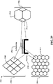
- FIG. 29 depicts cross-sections of exemplary PMUT arrays (2902, 2904, 2906) having high fill factor, in accordance with further non-limiting embodiments.
- FIG. 29 depicts exemplary PMUT arrays (2902, 2904, 2906) comprising PMUT structures in the exemplary PMUT arrays (2902, 2904, 2906) of PMUT structures that are configured in a rhombus configuration (2908, 2910) or a hexagonal configuration (2912, 2914).
- the exemplary PMUT arrays (2902) of PMUT structures can comprise PMUT structures that are configured in a rhombus configuration (2908)
- the exemplary PMUT arrays (2904) of PMUT structures can comprise PMUT structures that are configured in a hexagonal configuration (2912)
- the exemplary PMUT arrays (2906) of PMUT structures can comprise PMUT structures that are configured in a combination of rhombus configuration (2910) and hexagonal configuration (2914) arranged as a unit cell.
- edges of the PMUT structures between neighboring PMUT structures of the exemplary PMUT arrays can correspond to mechanical anchor 2918 points for the PMUT structure, for example, such as provided by aluminum-germanium eutectic bond between exemplary top metal layer 2812 of exemplary CMOS wafer 2802 and germanium layers 2728 on standoffs 2716 of exemplary PMUT 2700, as described above, regarding FIG. 27 , for example.
- mechanical anchor 2918 points for the PMUT structure for example, such as provided by aluminum-germanium eutectic bond between exemplary top metal layer 2812 of exemplary CMOS wafer 2802 and germanium layers 2728 on standoffs 2716 of exemplary PMUT 2700, as described above, regarding FIG. 27 , for example.
- Exemplary PMUT arrays (2902, 2904, 2906), as described herein, can provide high fill factor, thus increasing the array gain of exemplary PMUT arrays (2902, 2904, 2906).
- exemplary PMUT arrays (2902) of PMUT structures comprising PMUT structures configured in a hexagonal configuration (2912) can be formed in quadrilateral shape having angles of about 60 degrees.
- exemplary PMUT arrays (2904) of PMUT structures comprising PMUT structures configured in a rhombus configuration (2908) can be formed in quadrilateral shape having angles of about 60 degrees and about 120 degrees.
- FIG. 30 depicts a cross-section of exemplary PMUT for fingerprint sensing on IC comprising exemplary PMUT 3000 integrated on an exemplary CMOS wafer, in accordance with further non-limiting embodiments.
- an exemplary PMUT 3000 can be integrated on an exemplary CMOS wafer, as described below regarding FIGS. 31-45 .
- FIG. 31 depicts a cross-section 3100 of an exemplary CMOS wafer 3102 suitable for incorporation of aspects of the subject disclosure directed to fabrication of exemplary PMUT and PMUT arrays for fingerprint sensing on IC comprising exemplary one or more exemplary PMUTs integrated on exemplary CMOS wafer 3102, in accordance with further non-limiting embodiments.
- exemplary CMOS wafer 3102 can comprise exemplary source/drain regions 3104, gate 3106, one or more vias 3108, and one or more metal layers including a first metal layer 3110 and an exemplary top metal layer 3112.
- an exemplary top metal layer 3112 of exemplary CMOS wafer 3102 can comprise aluminum.
- exemplary CMOS wafer 3102 can comprise an exemplary silicon dioxide layer 3114 disposed over the exemplary top metal layer 3112 and an exemplary passivation layer 3116 disposed over the exemplary silicon dioxide layer 3114.
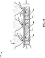
- FIG. 32 depicts a cross-section 3200 of an exemplary CMOS wafer 3102 comprising one or more exemplary cavities 3202, in accordance with further aspects described herein directed to a non-limiting cavity deposition etch process.
- exemplary passivation layer 3116 and exemplary silicon dioxide layer 3114 can be etched in a desired pattern with a timed etch is then performed to create the one or more exemplary cavities 3202.
- the one or more exemplary cavities 3202 can be created by employing a timed etch , resulting in an exemplary cavity depth of less than 0.8 ⁇ m (+/-10%).
- FIG. 33 depicts a cross-section 3300 of an exemplary CMOS wafer 3102 comprising one or more exemplary sacrificial materials 3302, in accordance with further aspects described herein directed to non-limiting amorphous silicon deposition and subsequent chemical-mechanical planarizing processes.
- one or more exemplary sacrificial materials 3302, e.g., such as amorphous silicon, etc. can be deposited in the one or more exemplary cavities 3202.
- the one or more exemplary sacrificial materials 3302 can comprise amorphous silicon.
- the one or more exemplary sacrificial materials 3302 can comprise silicon-germanium (SiGe) or tungsten (W), which including amorphous silicon are all CMOS foundry compatible materials and can be removed with xenon difluoride (XeF 2 ) or sulfur hexafluoride (SF 6 ).
- exemplary CMOS wafer 3102 comprising one or more exemplary sacrificial materials 3302 can be polished (e.g., chemical-mechanical planarizing) to planarize the surface, resulting in a sacrificial material film thickness of about less than 0.8 ⁇ m to prevent cracking and peeling of the sacrificial material film.
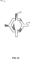
- FIG. 34 depicts a cross-section 3400 of an exemplary CMOS wafer 3102 comprising one or more exemplary silicon dioxide (SiO 2 ) layers 3402, in accordance with further aspects described herein directed to a non-limiting silicon dioxide deposition process.
- one or more exemplary silicon dioxide (SiO 2 ) layers 3402 can be deposited to cover the surface of the exemplary CMOS wafer 3102 comprising one or more exemplary sacrificial materials 3302 and serve as a structure material in the fabrication of one or more exemplary PMUTs integrated on exemplary CMOS wafer 3102, in accordance with further non-limiting embodiments.
- FIG. 35 depicts a cross-section 3500 of an exemplary CMOS wafer 3102 comprising one or more exemplary seal holes 3502, in accordance with further aspects described herein directed to a non-limiting release hole opening process.
- exemplary CMOS wafer 3102 comprising one or more exemplary silicon dioxide (SiO 2 ) layers 3402 can be etched to create one or more seal holes.
- SiO 2 silicon dioxide
- a seal hole profile having an aspect ratio greater than 4 can facilitate providing adequate sealing of the one or more exemplary cavities 3202.
- layout for the one or more exemplary cavities 3202 and one or more exemplary seal holes 3502 can comprise the one or more exemplary seal holes 3502 placed at the respective edges of the one or more exemplary cavities 3202, such that sealing of the one or more exemplary seal holes 3502 does not create an obstruction if the area in the one or more exemplary cavities 3202 directly underneath the one or more exemplary seal holes 3502 is fully filled, for example, as depicted in FIG. 35 .
- FIG. 36 depicts a cross-section 3600 of an exemplary CMOS wafer 3102 comprising one or more exemplary cavities 3202, in accordance with further aspects described herein directed to a non-limiting release etch process.
- exemplary CMOS wafer 3102 comprising the one or more exemplary seal holes 3502 and one or more exemplary sacrificial materials 3302 can be exposed to a sacrificial release etch to remove the one or more exemplary sacrificial materials 3302 ( e.g., amorphous silicon, etc. ) .
- exemplary CMOS wafer 3102 comprising the one or more exemplary seal holes 3502 and one or more exemplary sacrificial materials 3302 can be exposed to a sacrificial release etch employing either a dry etch or a wet etch.
- a sacrificial release etch employing either a dry etch or a wet etch.
- an exemplary dry etch can employ XeF2 or SF6 as etching gas.
- an exemplary wet etch can employ poly-etch (e.g., H:N:A, or a solution of Hydrofluoric Acid (HF):Nitric Acid (HNO 3 ):Acetic acid (CH 3 COOH) in a desired ratio), potassium hydroxide (KOH) or tetramethyl ammonium hydroxide (TMAH), with care taken to prevent stiction of the membrane created from the one or more exemplary silicon dioxide (SiO 2 ) layers 3402.
- poly-etch e.g., H:N:A, or a solution of Hydrofluoric Acid (HF):Nitric Acid (HNO 3 ):Acetic acid (CH 3 COOH) in a desired ratio
- KOH potassium hydroxide
- TMAH tetramethyl ammonium hydroxide
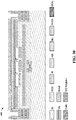
- FIG. 36 depicts exemplary CMOS wafer 3102 comprising one or more exemplary cavities 3202 and one or more exemplary unsealed seal holes 3602, for example, in inset 3604.
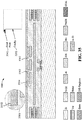
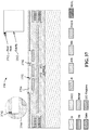
- FIG. 37 depicts a cross-section 3700 of an exemplary CMOS wafer 3102 comprising one or more exemplary seal hole seals 3702, in accordance with further aspects described herein directed to non-limiting seal deposition and etch back processes.
- exemplary CMOS wafer 3102 comprising one or more exemplary cavities 3202 and one or more exemplary unsealed seal holes 3602 can be exposed to a plasma-enhanced chemical vapor deposition (PECVD) process for SiO 2 deposition to create the one or more exemplary seal hole seals 3702 as depicted in inset 3704.
- PECVD of SiO 2 can create additional thickness of silicon dioxide which can be subject to an etch back process to control the final structure membrane thickness. It is further noted that, SiO 2 is defect tolerable for subsequent AlN deposition.
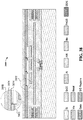
- FIG. 38 depicts a cross-section 3800 of an exemplary CMOS wafer 3102, in inset 3802, for example, comprising an exemplary aluminum nitride (AlN) seed layer 3804, molybdenum (Mo) layer 3806, and AlN stacking layer 3808, in accordance with further aspects described herein directed to non-limiting AlN Seed/Mo/AlN deposition processes, for example, as further describe above regarding FIGS. 9A-9K , 27 , etc.
- AlN aluminum nitride
- Mo molybdenum
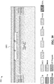
- FIG. 39 depicts a cross-section 3900 of an exemplary CMOS wafer 3102 comprising one or more exemplary SiO 2 layers 3902, in accordance with further aspects described herein directed to a non-limiting hard mask deposition process.
- FIG. 39 depicts a cross-section 3900 of an exemplary CMOS wafer 3102 comprising one or more exemplary SiO 2 layers 3902, in accordance with further aspects described herein directed to a non-limiting hard mask deposition process.
- FIG. 40 depicts a cross-section 4000 of an exemplary CMOS wafer 3102, in inset 4004 comprising one or more exemplary bottom contacts 4002, in accordance with further aspects described herein directed to a non-limiting bottom contact to molybdenum fabrication process.
- areas comprising AlN e.g., selected areas of AlN stacking layer 3808) over the one or more exemplary vias 4102 contact to exemplary top metal layer 3112 can also be etched to reduce etch difficulty in fabricating the one or more exemplary vias 4102 contact to exemplary top metal layer 3112.
- FIG. 41 depicts a cross-section 4100 of an exemplary CMOS wafer comprising 3102 one or more exemplary vias 4102, in accordance with further aspects described herein directed to a non-limiting wafer via etch process.
- the hard mask comprising one or more exemplary SiO 2 layers 3902 can be removed as shown in FIG. 42 , which depicts a cross-section 4200 of an exemplary CMOS wafer 3102 comprising an exposed AlN surface 4202 ( e.g., AlN stacking layer 3808), in accordance with further aspects described herein directed to a non-limiting hard mask removal process.
- FIG. 43 depicts a cross-section of an exemplary CMOS wafer comprising one or more exemplary SiO 2 spacers 4302, in accordance with further aspects described herein directed to a non-limiting SiO 2 spacer fabrication process.
- a layer of SiO 2 (not shown) can be deposited and blank etched ( e.g., without a mask material such as a photo resistive layer described above) to remove the top surface oxide completely while preserving the one or more exemplary SiO 2 spacers 4302.
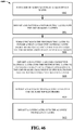
- FIG. 44 depicts a cross-section 4400 of an exemplary CMOS wafer 3102 comprising one or more exemplary top electrodes 4402, in accordance with further aspects described herein directed to a non-limiting top electrode fabrication process.
- one or more exemplary top electrodes 4402 material e.g., aluminum, etc.
- one or more exemplary top electrodes 4402 material can be deposited and patterned to form the one or more exemplary top electrodes 4402 for exemplary PMUT and PMUT arrays and to form electrical connection to exemplary top metal layer 3112 of exemplary CMOS wafer 3102.
- preserving the one or more exemplary SiO 2 spacers 4302 can prevent shorting of the one or more exemplary top electrodes 4402 and the one or more exemplary bottom contacts 4002 to the bottom electrode and exemplary aluminum nitride (AlN) seed layer 3804.
- AlN aluminum nitride
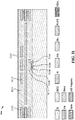
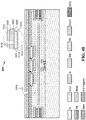
- FIG. 45 depicts exemplary PMUT for fingerprint sensing on IC comprising exemplary PMUT 3000 integrated on exemplary CMOS wafer 3102 as described above regarding FIGS. 30-44 , for which exemplary CMOS 3102 wafer comprises one or more exemplary passivation layers 4502, in accordance with further aspects described herein directed to a non-limiting passivation process.
- one or more exemplary passivation layers 4502 can be deposited on exemplary CMOS 3102 wafer and patterned to open one or more wire bond pads 4504 and/or one or more vias 4506 of exemplary PMUT 3000 integrated on exemplary CMOS wafer 3102.
- inset 4508 depicts various non-limiting aspects of exemplary PMUT 3000 integrated on exemplary CMOS wafer 3102, for example, as described above regarding FIGS. 31-45 .
- various non-limiting embodiments of the subject disclosure can comprise an exemplary MEMS device (e.g ., exemplary PMUT 2700 for fingerprint sensing on IC comprising exemplary PMUT 2700 bonded to an exemplary CMOS wafer 2802, exemplary PMUT 3000 integrated on exemplary CMOS wafer 3102, etc. ) , comprising a MUT structure (e.g., exemplary PMUT 2700 or portions thereof, exemplary PMUT 3000 or portions thereof, etc.
- exemplary MEMS device e.g ., exemplary PMUT 2700 for fingerprint sensing on IC comprising exemplary PMUT 2700 bonded to an exemplary CMOS wafer 2802, exemplary PMUT 3000 integrated on exemplary CMOS wafer 3102, etc.
- a MUT structure e.g., exemplary PMUT 2700 or portions thereof, exemplary PMUT 3000 or portions thereof, etc.
- a piezoelectric material e.g., one or more of aluminum nitride, lead zirconate titanate (PZT), zinc oxide, polyvinylidene difluoride (PVDF), lithium niobate (LiNbO3)
- the MEMS device e.g ., exemplary PMUT 2700 for fingerprint sensing on IC comprising exemplary PMUT 2700 bonded to an exemplary CMOS wafer 2802, exemplary PMUT 3000 integrated on exemplary CMOS wafer 3102, etc.
- a PMUT array of a fingerprint sensor adapted to sense a characteristic of a fingerprint placed adjacent to the MUT structure.
- exemplary MEMS device e.g ., exemplary PMUT 3000 integrated on exemplary CMOS wafer 3102, etc.
- a MUT structure e.g., exemplary PMUT 3000 or portions thereof, etc.
- CMOS structure e.g., exemplary CMOS wafer 3102 or portions thereof, etc.
- cavities e.g., one or more exemplary cavities 3202, etc.
- the piezoelectric material e.g., one or more of aluminum nitride, lead zirconate titanate (PZT), zinc oxide, polyvinylidene difluoride (PVDF), lithium niobate (LiNbO3) disposed on the CMOS structure.
- the piezoelectric material e.g., one or more of aluminum nitride, lead zirconate titanate (PZT), zinc oxide, polyvinylidene difluoride (PVDF), lithium niobate (LiNbO3)
- exemplary MEMS device e.g ., exemplary PMUT 2700 for fingerprint sensing on IC comprising exemplary PMUT 2700 bonded to an exemplary CMOS wafer 2802, exemplary PMUT 3000 integrated on exemplary CMOS wafer 3102, etc.
- a first metal conductive layer e.g., such as described regarding aluminum top electrode 2724, regarding one or more exemplary top electrodes 4402, etc., in reference to FIGS.
- the piezoelectric material e.g., one or more of aluminum nitride, lead zirconate titanate (PZT), zinc oxide, polyvinylidene difluoride (PVDF), lithium niobate (LiNbO3)).
- PZT lead zirconate titanate
- PVDF polyvinylidene difluoride
- LiNbO3 lithium niobate
- exemplary MEMS device e.g ., exemplary PMUT 2700 for fingerprint sensing on IC comprising exemplary PMUT 2700 bonded to an exemplary CMOS wafer 2802, exemplary PMUT 3000 integrated on exemplary CMOS wafer 3102, etc.
- exemplary MEMS device can further comprise a plurality of metal electrodes (e.g., one or more of aluminum top electrodes 2724, one or more bottom electrodes 2720, one or more exemplary top electrodes 4402, one or more exemplary bottom contacts 4002, etc. ) configured to form electrical connections between the first metal conductive layer (e.g., such as described regarding aluminum top electrode 2724, regarding one or more exemplary top electrodes 4402, etc., in reference to FIGS.
- metal electrodes e.g., one or more of aluminum top electrodes 2724, one or more bottom electrodes 2720, one or more exemplary top electrodes 4402, one or more exemplary bottom contacts 4002, etc.
- the piezoelectric material e.g., one or more of aluminum nitride, lead zirconate titanate (PZT), zinc oxide, polyvinylidene difluoride (PVDF), lithium niobate (LiNbO3)
- a CMOS structure e.g ., exemplary CMOS wafer 2802 or portions thereof, exemplary CMOS wafer 3102 or portions thereof, etc. , wherein the pMUT structure and the CMOS structure are vertically stacked, for example, as depicted in FIGS. 28 , 45 , etc.
- exemplary MEMS device e.g., exemplary PMUT 2700 for fingerprint sensing on IC comprising exemplary PMUT 2700 bonded to an exemplary CMOS wafer 2802, exemplary PMUT 3000 integrated on exemplary CMOS wafer 3102, etc.
- exemplary MEMS device can further comprise a second metal conductive layer (e.g ., molybdenum (Mo) layer 2712, molybdenum (Mo) layer 3806, etc.
- the piezoelectric material e.g., one or more of aluminum nitride, lead zirconate titanate (PZT), zinc oxide, polyvinylidene difluoride (PVDF), lithium niobate (LiNbO3)
- the piezoelectric material e.g., one or more of aluminum nitride, lead zirconate titanate (PZT), zinc oxide, polyvinylidene difluoride (PVDF), lithium niobate (LiNbO3)
- PZT lead zirconate titanate
- PVDF polyvinylidene difluoride
- LiNbO3 lithium niobate
- exemplary MEMS device e.g ., exemplary PMUT 2700 for fingerprint sensing on IC comprising exemplary PMUT 2700 bonded to an exemplary CMOS wafer 2802
- a stand-off e.g., one or more silicon dioxide standoffs 2716, etc.
- the piezoelectric material e.g., one or more of aluminum nitride, lead zirconate titanate (PZT), zinc oxide, polyvinylidene difluoride (PVDF), lithium niobate (LiNbO3)
- an exemplary stand-off e.g., one or more silicon dioxide standoffs 2716, etc.
- exemplary MEMS device e.g ., exemplary PMUT 2700 for fingerprint sensing on IC comprising exemplary PMUT 2700 bonded to an exemplary CMOS wafer 2802
- MUT structure e.g., exemplary PMUT 2700 or portions thereof, etc.
- CMOS structure e.g., exemplary CMOS wafer 2802 or portions thereof, etc.
- standoff e.g., one or more silicon dioxide standoffs 2716, etc.
- a eutectic bonding layer e.g., comprising an aluminum-germanium eutectic bonding layer, etc.
- a compression bond eutectic bonding layer
- exemplary MEMS device e.g., exemplary PMUT 2700 for fingerprint sensing on IC comprising exemplary PMUT 2700 bonded to an exemplary CMOS wafer 2802, exemplary PMUT 3000 integrated on exemplary CMOS wafer 3102, etc.
- exemplary MEMS device can further comprise a piezoelectric layer comprising an aluminum nitride (AlN) seed layer, a bottom metal layer, and an aluminum nitride (AlN) layer, for example, as further described herein.
- AlN aluminum nitride
- AlN aluminum nitride
- exemplary MEMS device e.g ., exemplary PMUT 2700 for fingerprint sensing on IC comprising exemplary PMUT 2700 bonded to an exemplary CMOS wafer 2802, exemplary PMUT 3000 integrated on exemplary CMOS wafer 3102, etc.
- a PMUT array as described herein, comprising the MUT structure (e.g ., exemplary PMUT 2700 or portions thereof, exemplary PMUT 3000 or portions thereof, etc. ) in an array of MUT structures (e.g., exemplary PMUT arrays (2902, 2904, 2906), etc.
- an exemplary MUT structure e.g., exemplary PMUT 2700 or portions thereof, exemplary PMUT 3000 or portions thereof, etc.
- the array of MUT structures e.g., exemplary PMUT arrays 2906, etc.
- ) can comprise a first two of the array of MUT structures in the rhombus configuration 2910 and a second two of the array of MUT structures in the hexagonal configuration 2914 arranged as a unit cell ( e.g., exemplary PMUT arrays 2906, etc. ) .
- an exemplary MEMS device e.g ., exemplary PMUT 3000 integrated on exemplary CMOS wafer 3102, etc.
- a CMOS device wafer e.g ., exemplary CMOS wafer 3102
- cavities e.g ., cavities 3202
- exemplary MEMS device e.g ., exemplary PMUT 3000 integrated on exemplary CMOS wafer 3102, etc.
- CMOS device wafer e.g., exemplary CMOS wafer 3102
- cavities e.g., cavities 3202
- exemplary MEMS device e.g., exemplary PMUT 3000 integrated on exemplary CMOS wafer 3102, etc.
- exemplary MEMS device can further comprise a piezoelectric material (e.g., one or more of aluminum nitride, lead zirconate titanate (PZT), zinc oxide, polyvinylidene difluoride (PVDF), lithium niobate (LiNbO3)) disposed on the first metal conductive layer (e.g., such as described regarding one or more exemplary top electrodes 4402, etc., in reference to FIG. 44 ).
- a piezoelectric material e.g., one or more of aluminum nitride, lead zirconate titanate (PZT), zinc oxide, polyvinylidene difluoride (PVDF), lithium niobate (LiNbO3)
- exemplary MEMS device e.g., exemplary PMUT 3000 integrated on exemplary CMOS wafer 3102, etc.
- exemplary MEMS device e.g., exemplary PMUT 3000 integrated on exemplary CMOS wafer 3102, etc.
- an exemplary acoustic propagation layer can be deposited over the one or more top electrodes ( e.g., one or more exemplary top electrodes 4402, etc. ) .
- exemplary MEMS device e.g., exemplary PMUT 3000 integrated on exemplary CMOS wafer 3102, etc.
- exemplary MEMS device can further comprise a second metal conductive layer (e.g., molybdenum (Mo) layer 3806, etc.
- Mo molybdenum
- the piezoelectric material e.g ., one or more of aluminum nitride, lead zirconate titanate (PZT), zinc oxide, polyvinylidene difluoride (PVDF), lithium niobate (LiNbO3)
- PZT lead zirconate titanate
- PVDF polyvinylidene difluoride
- LiNbO3 lithium niobate
- CMOS device wafer electrode e.g ., associated with exemplary top metal layer 3112
- the plurality of cavities e.g ., cavities 3202
- the piezoelectric material, the first metal conductive layer, and the second metal conductive layer are configured as a plurality of PMUT structures ( e.g., a plurality of exemplary PMUTs 3000, or portions thereof, integrated on exemplary CMOS wafer 3102, etc. ) .
- the plurality of PMUT structures can be formed integrally to a CMOS structure (e.g., exemplary CMOS wafer 3102, or portions thereof, etc. ) , and wherein the fingerprint sensor is adapted to sense a characteristic of a fingerprint placed adjacent to the PMUT array and opposite the plurality of cavities ( e.g ., cavities 3202).
- the plurality of PMUT structures e.g., a plurality of exemplary PMUTs 3000, or portions thereof, integrated on exemplary CMOS wafer 3102, etc.
- an exemplary PMUT structure e.g., exemplary PMUT 3000 or portions thereof, etc.
- the plurality of PMUT structures e.g., exemplary PMUT arrays 2906, etc.
- FIG. 46 depicts an exemplary flowchart of non-limiting methods 4600 associated with a various non-limiting embodiments of the subject disclosure.
- exemplary methods 4600 can comprise, at 4602, forming a plurality of cavities (e.g., cavities 3202) in a CMOS device wafer ( e.g., exemplary CMOS wafer 3102).
- forming the plurality of cavities at 4602 can comprise forming a PMUT (e.g ., exemplary PMUT 3000 integrated on exemplary CMOS wafer 3102, etc. ) array of a fingerprint sensor adapted to sense a characteristic of a fingerprint placed adjacent to the PMUT array and opposite the plurality of cavities (e.g. cavities 3202).
- forming the PMUT array comprises forming a plurality of PMUT devices in a rhombus configuration (2908), in a hexagonal configuration (2912), and/or in any combination thereof (e.g., exemplary PMUT arrays 2906), for example, as further described above regarding FIG. 29 .
- exemplary methods 4600 can further comprise forming a first two of the plurality of PMUT devices (e.g ., exemplary PMUT 3000 integrated on exemplary CMOS wafer 3102, etc.
- a second two of the plurality of PMUT devices e.g., exemplary PMUT 3000 integrated on exemplary CMOS wafer 3102, etc.
- the hexagonal configuration 2914 arranged as a unit cell ( e.g., exemplary PMUT arrays 2906, etc. ) .
- Exemplary methods 4600 can further comprise, at 4604, depositing and patterning a piezoelectric layer (e.g ., comprising aluminum nitride, lead zirconate titanate (PZT), zinc oxide, polyvinylidene difluoride (PVDF), lithium niobate (LiNbO3), etc. ) over the plurality of cavities (e.g., cavities 3202).
- a piezoelectric layer e.g ., comprising aluminum nitride, lead zirconate titanate (PZT), zinc oxide, polyvinylidene difluoride (PVDF), lithium niobate (LiNbO3), etc.
- exemplary methods 4600 can comprise, at 4606, forming a plurality of openings in the piezoelectric layer (e.g ., comprising aluminum nitride, lead zirconate titanate (PZT), zinc oxide, polyvinylidene difluoride (PVDF), lithium niobate (LiNbO3), etc. ) over the plurality of cavities ( e.g ., cavities 3202) to expose a first conductive material layer (e.g., molybdenum (Mo) layer 3806, etc. ) under the piezoelectric layer and to expose at least one CMOS device wafer (e.g ., exemplary CMOS wafer 3102) electrode (e.g ., associated with exemplary top metal layer 3112).
- CMOS device wafer e.g ., exemplary CMOS wafer 3102
- electrode e.g ., associated with exemplary top metal layer 3112
- exemplary methods 4600, at 4608 can further comprise depositing and patterning a second conductive material layer (e.g., such as described regarding one or more exemplary top electrodes 4402, etc., in reference to FIG. 44 ) over the piezoelectric layer (e.g ., comprising aluminum nitride, lead zirconate titanate (PZT), zinc oxide, polyvinylidene difluoride (PVDF), lithium niobate (LiNbO3), etc.
- a second conductive material layer e.g., such as described regarding one or more exemplary top electrodes 4402, etc., in reference to FIG. 44
- the piezoelectric layer e.g ., comprising aluminum nitride, lead zirconate titanate (PZT), zinc oxide, polyvinylidene difluoride (PVDF), lithium niobate (LiNbO3), etc.
- exemplary methods 4600 can further comprise, at 4608, forming one or more bottom electrodes ( e.g., one or more exemplary bottom contacts 4002, etc. ) electrically coupled to one or more top electrodes ( e.g., one or more exemplary top electrodes 4402, etc. ) via the piezoelectric layer.
- CMOS device wafer e.g., exemplary CMOS wafer 3102
- electrode e.g., associated with exemplary top metal layer 3112
- exemplary methods 4600 can further comprise, at 4608, forming one or more bottom electrodes ( e.g., one or more exemplary bottom contacts 4002, etc. ) electrically coupled to one or more top electrodes ( e.g., one or more exemplary top electrodes 4402, etc. ) via the piezoelectric layer.
- Exemplary methods 4600, at 4610 can further comprise depositing an acoustic propagation layer over the one or more top electrodes (e.g., one or more exemplary top electrodes 4402, etc. ) , for example, as further described above, for example, regarding FIG. 18 .
- an exemplary acoustic propagation layer comprising a liquid, a polymer, or an acoustic impedance matching material configured to provide acoustic impedance matching between a PMUT device (e.g., exemplary PMUT 3000 integrated on exemplary CMOS wafer 3102, etc.
- exemplary methods 4600, at 4612 can further comprise depositing a cover layer over the acoustic propagation layer, to facilitate providing further protection to the PMUT device ( e.g ., exemplary PMUT 3000 integrated on exemplary CMOS wafer 3102, etc. ) from debris, contaminants, etc. from introducing errors in measurements associated with PMUT device ( e.g ., exemplary PMUT 3000 integrated on exemplary CMOS wafer 3102, etc. ) .
- FIG. 47 depicts another exemplary flowchart of non-limiting methods associated with a various non-limiting embodiments of the subject disclosure.
- exemplary methods 4700 can comprise forming a plurality of cavities (e.g ., cavities 3202) in a CMOS device wafer ( e.g ., exemplary CMOS wafer 3102).
- exemplary methods 4700, at 4702 can comprise filling the plurality of cavities (e.g., cavities 3202) in the CMOS device wafer (e.g., exemplary CMOS wafer 3102) with sacrificial material (e.g ., one or more exemplary sacrificial materials 3302, amorphous silicon, etc.
- sacrificial material e.g ., one or more exemplary sacrificial materials 3302, amorphous silicon, etc.
- exemplary methods 4700, at 4704 can comprise planarizing the sacrificial material (e.g., one or more exemplary sacrificial materials 3302, amorphous silicon, etc. ) on the CMOS device wafer ( e.g ., exemplary CMOS wafer 3102), and at 4706, can further comprise depositing a capping layer (e.g., one or more exemplary silicon dioxide (SiO 2 ) layers 3402, etc. ) over the sacrificial material (e.g., one or more exemplary sacrificial materials 3302, amorphous silicon, etc. ) .
- a capping layer e.g., one or more exemplary silicon dioxide (SiO 2 ) layers 3402, etc.
- Exemplary methods 4700, at 4708 can further comprise forming one or more openings (e.g., one or more exemplary seal holes 3502) in the capping layer (e.g., one or more exemplary silicon dioxide (SiO 2 ) layers 3402, etc. ) to expose the sacrificial material (e.g ., one or more exemplary sacrificial materials 3302, amorphous silicon, etc. ) , and at 4710, can further comprise selectively removing the sacrificial material.
- exemplary methods 4700, at 4712 can further comprise sealing the one or more openings in the capping layer (e.g., one or more exemplary silicon dioxide (SiO 2 ) layers 3402, etc.
- the first conductive material layer e.g., molybdenum (Mo) layer 3806, etc.
- a metal conductive layer over the capping layer (e.g., one or more exemplary silicon dioxide (SiO 2 ) layers 3402, etc. ) .
- example and/or exemplary are used herein to mean serving as an example, instance, or illustration. Any aspect or design described herein as “example” and/or “exemplary” is not necessarily to be construed as preferred or advantageous over other aspects or designs. Rather, use of the word exemplary is intended to present concepts in a concrete fashion.
Landscapes
- Engineering & Computer Science (AREA)
- Manufacturing & Machinery (AREA)
- Human Computer Interaction (AREA)
- Physics & Mathematics (AREA)
- General Physics & Mathematics (AREA)
- Multimedia (AREA)
- Theoretical Computer Science (AREA)
- Micromachines (AREA)
- Piezo-Electric Transducers For Audible Bands (AREA)
- Piezo-Electric Or Mechanical Vibrators, Or Delay Or Filter Circuits (AREA)
Claims (7)
- Dispositif de systèmes microélectromécaniques, MEMS, comprenant:une plaquette de dispositif CMOS (métal-oxyde-semiconducteur) complémentaire (3102), la plaquette de dispositif CMOS comprenant au moins deux électrodes de plaquette de dispositif CMSOS, associées à un premier réseau de structures de transducteur ultrasonore MEMS piézoélectrique, PMUT, (3000, 2902, 2904, 2906) d'un capteur d'empreintes digitales et ayant une pluralité de cavités configurées dans un second réseau;une première couche métallique conductrice (4402) disposée sur la plaquette du dispositif CMOS et sur la pluralité de cavités;un matériau piézoélectrique disposé sur la première couche métallique conductrice; etune seconde couche conductrice métallique, (3806), disposée sur le matériau piézoélectrique, couplant électriquement la seconde couche conductrice métallique et au moins une électrode de tranche de dispositif CMOS, et couplant électriquement la première couche conductrice métallique à au moins une autre électrode de tranche de dispositif CMOS, dans lequel la pluralité de cavités, le matériau piézoélectrique, la première couche conductrice métallique et la seconde couche conductrice métallique sont configurés comme un réseau de structures PMUT.
- Dispositif MEMS selon la revendication 1, dans lequel le réseau de structures PMUT est formé intégralement à la plaquette du dispositif CMOS, et dans lequel le capteur d'empreintes digitales est conçu pour détecter une caractéristique d'une empreinte digitale placée à côté du réseau PMUT et en face du seconde réseau de cavités.
- Dispositif MEMS selon la revendication 1, dans lequel le réseau de structures PMUT comprend le réseau de structures PMUT dans au moins une configuration en losange (2908, 2910) ou une configuration hexagonale (2912, 2914).
- Dispositif MEMS selon la revendication 3, dans lequel le réseau de structures PMUT comprend deux premières structures du réseau de structures PMUT dans la configuration en losange et deux secondes structures du réseau de structures PMUT dans la configuration hexagonale disposées comme une cellule unitaire.
- Dispositif MEMS selon la revendication 1, dans lequel le matériau piézoélectrique comprend au moins un des éléments suivants: nitrure d'aluminium, titanate de zirconate de plomb, PZT, oxyde de zinc, difluorure de polyvinylidène, PVDF, niobate de lithium, LiNbO3.
- Dispositif MEMS de la revendication 1, comprenant en outre:
au moins une électrode inférieure couplée électriquement à au moins une électrode supérieure via le matériau piézoélectrique. - Dispositif MEMS de la revendication 6, comprenant en outre:
une couche de propagation acoustique disposée sur au moins une électrode supérieure.
Priority Applications (1)
| Application Number | Priority Date | Filing Date | Title |
|---|---|---|---|
| EP20185765.3A EP3757884B1 (fr) | 2014-09-08 | 2015-09-08 | Transducteur ultrasonore piézoélectrique micro-usiné (pmut) intégré sur circuit intégré (ic) pour détection d'empreintes digitales |
Applications Claiming Priority (4)
| Application Number | Priority Date | Filing Date | Title |
|---|---|---|---|
| US14/480,051 US9511994B2 (en) | 2012-11-28 | 2014-09-08 | Aluminum nitride (AlN) devices with infrared absorption structural layer |
| US201562153480P | 2015-04-27 | 2015-04-27 | |
| US14/829,404 US10497747B2 (en) | 2012-11-28 | 2015-08-18 | Integrated piezoelectric microelectromechanical ultrasound transducer (PMUT) on integrated circuit (IC) for fingerprint sensing |
| PCT/US2015/048964 WO2016040333A2 (fr) | 2014-09-08 | 2015-09-08 | Transducteur ultrasonore piézoélectrique micro-usiné (pmut) intégré (pmut) sur circuit intégré (ic) pour détection d'empreintes digitales |
Related Child Applications (2)
| Application Number | Title | Priority Date | Filing Date |
|---|---|---|---|
| EP20185765.3A Division EP3757884B1 (fr) | 2014-09-08 | 2015-09-08 | Transducteur ultrasonore piézoélectrique micro-usiné (pmut) intégré sur circuit intégré (ic) pour détection d'empreintes digitales |
| EP20185765.3A Division-Into EP3757884B1 (fr) | 2014-09-08 | 2015-09-08 | Transducteur ultrasonore piézoélectrique micro-usiné (pmut) intégré sur circuit intégré (ic) pour détection d'empreintes digitales |
Publications (2)
| Publication Number | Publication Date |
|---|---|
| EP3292508A2 EP3292508A2 (fr) | 2018-03-14 |
| EP3292508B1 true EP3292508B1 (fr) | 2020-12-23 |
Family
ID=54186293
Family Applications (2)
| Application Number | Title | Priority Date | Filing Date |
|---|---|---|---|
| EP15767646.1A Active EP3292508B1 (fr) | 2014-09-08 | 2015-09-08 | Transducteur ultrasonore piézoélectrique micro-usiné (pmut) intégré (pmut) sur circuit intégré (ic) pour détection d'empreintes digitales |
| EP20185765.3A Active EP3757884B1 (fr) | 2014-09-08 | 2015-09-08 | Transducteur ultrasonore piézoélectrique micro-usiné (pmut) intégré sur circuit intégré (ic) pour détection d'empreintes digitales |
Family Applications After (1)
| Application Number | Title | Priority Date | Filing Date |
|---|---|---|---|
| EP20185765.3A Active EP3757884B1 (fr) | 2014-09-08 | 2015-09-08 | Transducteur ultrasonore piézoélectrique micro-usiné (pmut) intégré sur circuit intégré (ic) pour détection d'empreintes digitales |
Country Status (2)
| Country | Link |
|---|---|
| EP (2) | EP3292508B1 (fr) |
| WO (1) | WO2016040333A2 (fr) |
Cited By (15)
| Publication number | Priority date | Publication date | Assignee | Title |
|---|---|---|---|---|
| US11288891B2 (en) | 2016-05-10 | 2022-03-29 | Invensense, Inc. | Operating a fingerprint sensor comprised of ultrasonic transducers |
| US11328165B2 (en) | 2020-04-24 | 2022-05-10 | Invensense, Inc. | Pressure-based activation of fingerprint spoof detection |
| US11392789B2 (en) | 2019-10-21 | 2022-07-19 | Invensense, Inc. | Fingerprint authentication using a synthetic enrollment image |
| US11440052B2 (en) | 2016-05-04 | 2022-09-13 | Invensense, Inc. | Two-dimensional array of CMOS control elements |
| US11460957B2 (en) | 2020-03-09 | 2022-10-04 | Invensense, Inc. | Ultrasonic fingerprint sensor with a contact layer of non-uniform thickness |
| US11471912B2 (en) | 2016-05-10 | 2022-10-18 | Invensense, Inc. | Supplemental sensor modes and systems for ultrasonic transducers |
| US11626099B2 (en) | 2016-05-10 | 2023-04-11 | Invensense, Inc. | Transmit beamforming of a two-dimensional array of ultrasonic transducers |
| US11651611B2 (en) * | 2016-05-04 | 2023-05-16 | Invensense, Inc. | Device mountable packaging of ultrasonic transducers |
| US11673165B2 (en) | 2016-05-10 | 2023-06-13 | Invensense, Inc. | Ultrasonic transducer operable in a surface acoustic wave (SAW) mode |
| US11682228B2 (en) | 2019-07-17 | 2023-06-20 | Invensense, Inc. | Ultrasonic fingerprint sensor with a contact layer of non-uniform thickness |
| US11995909B2 (en) | 2020-07-17 | 2024-05-28 | Tdk Corporation | Multipath reflection correction |
| US12002282B2 (en) | 2018-03-22 | 2024-06-04 | Invensense, Inc. | Operating a fingerprint sensor comprised of ultrasonic transducers |
| US12174295B2 (en) | 2020-08-07 | 2024-12-24 | Tdk Corporation | Acoustic multipath correction |
| US12197681B2 (en) | 2021-08-25 | 2025-01-14 | Tdk Corporation | Anchor configurations for an array of ultrasonic transducers |
| US12416807B2 (en) | 2021-08-20 | 2025-09-16 | Tdk Corporation | Retinal projection display system |
Families Citing this family (32)
| Publication number | Priority date | Publication date | Assignee | Title |
|---|---|---|---|---|
| WO2017165146A1 (fr) * | 2016-03-23 | 2017-09-28 | Invensense, Inc. | Intégration d'un transducteur ultrasonore sur un substrat cmos au moyen d'un processus de collage par fusion |
| US10670716B2 (en) | 2016-05-04 | 2020-06-02 | Invensense, Inc. | Operating a two-dimensional array of ultrasonic transducers |
| US10656255B2 (en) | 2016-05-04 | 2020-05-19 | Invensense, Inc. | Piezoelectric micromachined ultrasonic transducer (PMUT) |
| US10325915B2 (en) | 2016-05-04 | 2019-06-18 | Invensense, Inc. | Two-dimensional array of CMOS control elements |
| CN109314175B (zh) * | 2016-05-04 | 2023-07-25 | 应美盛公司 | Cmos控制元件的二维阵列 |
| US10632500B2 (en) | 2016-05-10 | 2020-04-28 | Invensense, Inc. | Ultrasonic transducer with a non-uniform membrane |
| US10562070B2 (en) | 2016-05-10 | 2020-02-18 | Invensense, Inc. | Receive operation of an ultrasonic sensor |
| US10408797B2 (en) | 2016-05-10 | 2019-09-10 | Invensense, Inc. | Sensing device with a temperature sensor |
| US10600403B2 (en) | 2016-05-10 | 2020-03-24 | Invensense, Inc. | Transmit operation of an ultrasonic sensor |
| US10539539B2 (en) | 2016-05-10 | 2020-01-21 | Invensense, Inc. | Operation of an ultrasonic sensor |
| US10891461B2 (en) | 2017-05-22 | 2021-01-12 | Invensense, Inc. | Live fingerprint detection utilizing an integrated ultrasound and infrared sensor |
| US10474862B2 (en) | 2017-06-01 | 2019-11-12 | Invensense, Inc. | Image generation in an electronic device using ultrasonic transducers |
| US10643052B2 (en) | 2017-06-28 | 2020-05-05 | Invensense, Inc. | Image generation in an electronic device using ultrasonic transducers |
| MY191624A (en) | 2017-09-29 | 2022-07-04 | Silterra Malaysia Sdn Bhd | Monolithic integration of pmut on cmos |
| US10984209B2 (en) | 2017-12-01 | 2021-04-20 | Invensense, Inc. | Darkfield modeling |
| WO2019109010A1 (fr) | 2017-12-01 | 2019-06-06 | Invensense, Inc. | Suivi de fond noir |
| US10997388B2 (en) | 2017-12-01 | 2021-05-04 | Invensense, Inc. | Darkfield contamination detection |
| US11151355B2 (en) | 2018-01-24 | 2021-10-19 | Invensense, Inc. | Generation of an estimated fingerprint |
| US11623246B2 (en) | 2018-02-26 | 2023-04-11 | Invensense, Inc. | Piezoelectric micromachined ultrasound transducer device with piezoelectric barrier layer |
| CN109244232B (zh) * | 2018-09-13 | 2023-07-04 | 徐景辉 | 微机电系统压电换能器及制作方法 |
| WO2020102564A1 (fr) | 2018-11-14 | 2020-05-22 | Invensense, Inc. | Dispositif transducteur ultrasonore micro-usiné piézoélectrique à deux électrodes |
| CN113316486B (zh) | 2018-11-16 | 2022-10-18 | 维蒙股份公司 | 电容式微机械超声换能器及其制造方法 |
| US10936843B2 (en) | 2018-12-28 | 2021-03-02 | Invensense, Inc. | Segmented image acquisition |
| US11188735B2 (en) | 2019-06-24 | 2021-11-30 | Invensense, Inc. | Fake finger detection using ridge features |
| US11216681B2 (en) | 2019-06-25 | 2022-01-04 | Invensense, Inc. | Fake finger detection based on transient features |
| US11216632B2 (en) | 2019-07-17 | 2022-01-04 | Invensense, Inc. | Ultrasonic fingerprint sensor with a contact layer of non-uniform thickness |
| US11232549B2 (en) | 2019-08-23 | 2022-01-25 | Invensense, Inc. | Adapting a quality threshold for a fingerprint image |
| US11243300B2 (en) | 2020-03-10 | 2022-02-08 | Invensense, Inc. | Operating a fingerprint sensor comprised of ultrasonic transducers and a presence sensor |
| WO2021205685A1 (fr) * | 2020-04-09 | 2021-10-14 | 株式会社村田製作所 | Procédé destiné à fabriquer un substrat d'assemblage, et substrat d'assemblage |
| CN111864053A (zh) * | 2020-07-24 | 2020-10-30 | 深圳市汇顶科技股份有限公司 | 超声传感器制备方法、超声传感器以及电子设备 |
| CN114620673B (zh) * | 2022-03-18 | 2022-11-15 | 浙江仙声科技有限公司 | Cmut结合mems压力传感器的超声换能器单元、阵列及制造方法 |
| CN119629554A (zh) * | 2023-09-13 | 2025-03-14 | 天津大学 | 压电mems换能器装置、其制造方法以及包括其的电子设备 |
Citations (1)
| Publication number | Priority date | Publication date | Assignee | Title |
|---|---|---|---|---|
| US20140219063A1 (en) * | 2013-02-07 | 2014-08-07 | Arman HAJATI | Micromachined ultrasonic transducer devices with metal-semiconductor contact for reduced capacitive cross-talk |
Family Cites Families (3)
| Publication number | Priority date | Publication date | Assignee | Title |
|---|---|---|---|---|
| KR100561851B1 (ko) * | 2003-11-18 | 2006-03-16 | 삼성전자주식회사 | 지문 인식 센서 및 그 제조 방법 |
| US9114977B2 (en) * | 2012-11-28 | 2015-08-25 | Invensense, Inc. | MEMS device and process for RF and low resistance applications |
| KR102305274B1 (ko) * | 2013-07-16 | 2021-09-24 | 더 리젠트스 오브 더 유니이버시티 오브 캘리포니아 | Mut 지문 id 시스템 |
-
2015
- 2015-09-08 EP EP15767646.1A patent/EP3292508B1/fr active Active
- 2015-09-08 WO PCT/US2015/048964 patent/WO2016040333A2/fr not_active Ceased
- 2015-09-08 EP EP20185765.3A patent/EP3757884B1/fr active Active
Patent Citations (1)
| Publication number | Priority date | Publication date | Assignee | Title |
|---|---|---|---|---|
| US20140219063A1 (en) * | 2013-02-07 | 2014-08-07 | Arman HAJATI | Micromachined ultrasonic transducer devices with metal-semiconductor contact for reduced capacitive cross-talk |
Non-Patent Citations (3)
| Title |
|---|
| H. TANG ET AL: "Pulse-echo ultrasonic fingerprint sensor on a chip", 2015 TRANSDUCERS, 2015 18TH INTERNATIONAL CONFERENCE ON SOLID-STATE SENSORS, ACTUATORS AND MICROSYSTEMS (TRANSDUCERS), 1 April 2015 (2015-04-01), pages 674 - 677, XP055309421, ISBN: 978-1-4799-8955-3, DOI: 10.1109/TRANSDUCERS.2015.7181013 * |
| SAVOIA A ET AL: "Design and fabrication of a cMUT probe for ultrasound imaging of fingerprints", ULTRASONICS SYMPOSIUM (IUS), 2010 IEEE, IEEE, 11 October 2010 (2010-10-11), pages 1877 - 1880, XP032393427, ISBN: 978-1-4577-0382-9, DOI: 10.1109/ULTSYM.2010.5935836 * |
| TSAI J M ET AL: "Versatile CMOS-MEMS integrated piezoelectric platform", 2015 TRANSDUCERS - 2015 18TH INTERNATIONAL CONFERENCE ON SOLID-STATE SENSORS, ACTUATORS AND MICROSYSTEMS (TRANSDUCERS), IEEE, 21 June 2015 (2015-06-21), pages 2248 - 2251, XP033189793, DOI: 10.1109/TRANSDUCERS.2015.7181409 * |
Cited By (17)
| Publication number | Priority date | Publication date | Assignee | Title |
|---|---|---|---|---|
| US11440052B2 (en) | 2016-05-04 | 2022-09-13 | Invensense, Inc. | Two-dimensional array of CMOS control elements |
| US11651611B2 (en) * | 2016-05-04 | 2023-05-16 | Invensense, Inc. | Device mountable packaging of ultrasonic transducers |
| US11288891B2 (en) | 2016-05-10 | 2022-03-29 | Invensense, Inc. | Operating a fingerprint sensor comprised of ultrasonic transducers |
| US11471912B2 (en) | 2016-05-10 | 2022-10-18 | Invensense, Inc. | Supplemental sensor modes and systems for ultrasonic transducers |
| US11626099B2 (en) | 2016-05-10 | 2023-04-11 | Invensense, Inc. | Transmit beamforming of a two-dimensional array of ultrasonic transducers |
| US11673165B2 (en) | 2016-05-10 | 2023-06-13 | Invensense, Inc. | Ultrasonic transducer operable in a surface acoustic wave (SAW) mode |
| US12002282B2 (en) | 2018-03-22 | 2024-06-04 | Invensense, Inc. | Operating a fingerprint sensor comprised of ultrasonic transducers |
| US11682228B2 (en) | 2019-07-17 | 2023-06-20 | Invensense, Inc. | Ultrasonic fingerprint sensor with a contact layer of non-uniform thickness |
| US11392789B2 (en) | 2019-10-21 | 2022-07-19 | Invensense, Inc. | Fingerprint authentication using a synthetic enrollment image |
| US11460957B2 (en) | 2020-03-09 | 2022-10-04 | Invensense, Inc. | Ultrasonic fingerprint sensor with a contact layer of non-uniform thickness |
| US11328165B2 (en) | 2020-04-24 | 2022-05-10 | Invensense, Inc. | Pressure-based activation of fingerprint spoof detection |
| US11995909B2 (en) | 2020-07-17 | 2024-05-28 | Tdk Corporation | Multipath reflection correction |
| US12174295B2 (en) | 2020-08-07 | 2024-12-24 | Tdk Corporation | Acoustic multipath correction |
| US12416807B2 (en) | 2021-08-20 | 2025-09-16 | Tdk Corporation | Retinal projection display system |
| US12197681B2 (en) | 2021-08-25 | 2025-01-14 | Tdk Corporation | Anchor configurations for an array of ultrasonic transducers |
| US12260050B2 (en) | 2021-08-25 | 2025-03-25 | Tdk Corporation | Differential receive at an ultrasonic transducer |
| US12578825B2 (en) | 2021-08-25 | 2026-03-17 | Tdk Corporation | Anchor configurations for an array of ultrasonic transducers |
Also Published As
| Publication number | Publication date |
|---|---|
| WO2016040333A2 (fr) | 2016-03-17 |
| WO2016040333A3 (fr) | 2016-05-06 |
| EP3757884A1 (fr) | 2020-12-30 |
| EP3292508A2 (fr) | 2018-03-14 |
| EP3757884B1 (fr) | 2025-04-16 |
Similar Documents
| Publication | Publication Date | Title |
|---|---|---|
| US11847851B2 (en) | Integrated piezoelectric microelectromechanical ultrasound transducer (PMUT) on integrated circuit (IC) for fingerprint sensing | |
| EP3757884B1 (fr) | Transducteur ultrasonore piézoélectrique micro-usiné (pmut) intégré sur circuit intégré (ic) pour détection d'empreintes digitales | |
| US20200111834A1 (en) | Integrated piezoelectric microelectromechanical ultrasound transducer (pmut) on integrated circuit (ic) for fingerprint sensing | |
| US11577276B2 (en) | Piezoelectric micromachined ultrasound transducer device with multi-layer etched isolation trench | |
| US9511994B2 (en) | Aluminum nitride (AlN) devices with infrared absorption structural layer | |
| JP5891571B2 (ja) | Mems圧力センサ装置及びその作製方法 | |
| JP5806254B2 (ja) | 単結晶シリコン電極を備えた容量性微小電気機械式センサー | |
| US7993949B2 (en) | Heterogeneous substrate including a sacrificial layer, and a method of fabricating it | |
| US9194882B2 (en) | Inertial and pressure sensors on single chip | |
| US20190218093A1 (en) | Monolithically integrated multi-sensor device on a semiconductor substrate and method therefor | |
| EP3052901B1 (fr) | Capteurs inertiels et de pression sur une seule puce | |
| US20100029031A1 (en) | Method of fabricating a mems/nems electromechanical component | |
| JP2007210083A (ja) | Mems素子及びその製造方法 | |
| TW201604121A (zh) | 微電機構件以及製造微電機構件的方法 | |
| JP2012127966A (ja) | センサーを製作するための方法 | |
| JP5592087B2 (ja) | 半導体装置及び半導体装置の製造方法 | |
| Park et al. | Fabricating capacitive micromachined ultrasonic transducers with direct wafer-bonding and LOCOS technology | |
| CN101567394B (zh) | 一种垂直环绕栅结型场效应晶体管、制作方法及应用 | |
| Chen et al. | Wafer-level epitaxial silicon packaging for out-of-plane RF MEMS resonators with integrated actuation electrodes | |
| Torunbalci | Development of new, simple, and robust wafer level hermetic packaging methods for MEMS sensors | |
| Chaudhuri et al. | CMOS integrated poly-sigemems accelerometer above 0.18 µm technology | |
| RU2435294C2 (ru) | Способ изготовления интегрального высокодобротного кремниевого микромеханического резонатора | |
| US20090017305A1 (en) | Manufacturing process for integrated microelectromechanical components | |
| US10524059B2 (en) | Capacitive-based transducer with high aspect ratio | |
| Chow et al. | MEMS Inertia Sensors in Semi-Standard Processes–Transiting from University’s Laboratory to a CMOS-MEMS Foundry |
Legal Events
| Date | Code | Title | Description |
|---|---|---|---|
| STAA | Information on the status of an ep patent application or granted ep patent |
Free format text: STATUS: THE INTERNATIONAL PUBLICATION HAS BEEN MADE |
|
| STAA | Information on the status of an ep patent application or granted ep patent |
Free format text: STATUS: THE APPLICATION IS DEEMED TO BE WITHDRAWN |
|
| STAA | Information on the status of an ep patent application or granted ep patent |
Free format text: STATUS: THE INTERNATIONAL PUBLICATION HAS BEEN MADE |
|
| PUAI | Public reference made under article 153(3) epc to a published international application that has entered the european phase |
Free format text: ORIGINAL CODE: 0009012 |
|
| STAA | Information on the status of an ep patent application or granted ep patent |
Free format text: STATUS: REQUEST FOR EXAMINATION WAS MADE |
|
| 17P | Request for examination filed |
Effective date: 20171229 |
|
| AK | Designated contracting states |
Kind code of ref document: A2 Designated state(s): AL AT BE BG CH CY CZ DE DK EE ES FI FR GB GR HR HU IE IS IT LI LT LU LV MC MK MT NL NO PL PT RO RS SE SI SK SM TR |
|
| PUAG | Search results despatched under rule 164(2) epc together with communication from examining division |
Free format text: ORIGINAL CODE: 0009017 |
|
| STAA | Information on the status of an ep patent application or granted ep patent |
Free format text: STATUS: EXAMINATION IS IN PROGRESS |
|
| 17Q | First examination report despatched |
Effective date: 20190226 |
|
| B565 | Issuance of search results under rule 164(2) epc |
Effective date: 20190226 |
|
| RIC1 | Information provided on ipc code assigned before grant |
Ipc: G06K 9/00 20060101AFI20190221BHEP Ipc: H03H 3/007 20060101ALI20190221BHEP |
|
| GRAP | Despatch of communication of intention to grant a patent |
Free format text: ORIGINAL CODE: EPIDOSNIGR1 |
|
| STAA | Information on the status of an ep patent application or granted ep patent |
Free format text: STATUS: GRANT OF PATENT IS INTENDED |
|
| INTG | Intention to grant announced |
Effective date: 20200214 |
|
| GRAJ | Information related to disapproval of communication of intention to grant by the applicant or resumption of examination proceedings by the epo deleted |
Free format text: ORIGINAL CODE: EPIDOSDIGR1 |
|
| STAA | Information on the status of an ep patent application or granted ep patent |
Free format text: STATUS: EXAMINATION IS IN PROGRESS |
|
| GRAP | Despatch of communication of intention to grant a patent |
Free format text: ORIGINAL CODE: EPIDOSNIGR1 |
|
| STAA | Information on the status of an ep patent application or granted ep patent |
Free format text: STATUS: GRANT OF PATENT IS INTENDED |
|
| INTC | Intention to grant announced (deleted) | ||
| INTG | Intention to grant announced |
Effective date: 20200729 |
|
| GRAS | Grant fee paid |
Free format text: ORIGINAL CODE: EPIDOSNIGR3 |
|
| GRAA | (expected) grant |
Free format text: ORIGINAL CODE: 0009210 |
|
| STAA | Information on the status of an ep patent application or granted ep patent |
Free format text: STATUS: THE PATENT HAS BEEN GRANTED |
|
| AK | Designated contracting states |
Kind code of ref document: B1 Designated state(s): AL AT BE BG CH CY CZ DE DK EE ES FI FR GB GR HR HU IE IS IT LI LT LU LV MC MK MT NL NO PL PT RO RS SE SI SK SM TR |
|
| REG | Reference to a national code |
Ref country code: GB Ref legal event code: FG4D |
|
| REG | Reference to a national code |
Ref country code: DE Ref legal event code: R096 Ref document number: 602015063844 Country of ref document: DE |
|
| REG | Reference to a national code |
Ref country code: AT Ref legal event code: REF Ref document number: 1348440 Country of ref document: AT Kind code of ref document: T Effective date: 20210115 |
|
| REG | Reference to a national code |
Ref country code: IE Ref legal event code: FG4D |
|
| PG25 | Lapsed in a contracting state [announced via postgrant information from national office to epo] |
Ref country code: GR Free format text: LAPSE BECAUSE OF FAILURE TO SUBMIT A TRANSLATION OF THE DESCRIPTION OR TO PAY THE FEE WITHIN THE PRESCRIBED TIME-LIMIT Effective date: 20210324 Ref country code: RS Free format text: LAPSE BECAUSE OF FAILURE TO SUBMIT A TRANSLATION OF THE DESCRIPTION OR TO PAY THE FEE WITHIN THE PRESCRIBED TIME-LIMIT Effective date: 20201223 Ref country code: FI Free format text: LAPSE BECAUSE OF FAILURE TO SUBMIT A TRANSLATION OF THE DESCRIPTION OR TO PAY THE FEE WITHIN THE PRESCRIBED TIME-LIMIT Effective date: 20201223 Ref country code: NO Free format text: LAPSE BECAUSE OF FAILURE TO SUBMIT A TRANSLATION OF THE DESCRIPTION OR TO PAY THE FEE WITHIN THE PRESCRIBED TIME-LIMIT Effective date: 20210323 |
|
| REG | Reference to a national code |
Ref country code: AT Ref legal event code: MK05 Ref document number: 1348440 Country of ref document: AT Kind code of ref document: T Effective date: 20201223 |
|
| REG | Reference to a national code |
Ref country code: NL Ref legal event code: MP Effective date: 20201223 |
|
| PG25 | Lapsed in a contracting state [announced via postgrant information from national office to epo] |
Ref country code: LV Free format text: LAPSE BECAUSE OF FAILURE TO SUBMIT A TRANSLATION OF THE DESCRIPTION OR TO PAY THE FEE WITHIN THE PRESCRIBED TIME-LIMIT Effective date: 20201223 Ref country code: SE Free format text: LAPSE BECAUSE OF FAILURE TO SUBMIT A TRANSLATION OF THE DESCRIPTION OR TO PAY THE FEE WITHIN THE PRESCRIBED TIME-LIMIT Effective date: 20201223 Ref country code: BG Free format text: LAPSE BECAUSE OF FAILURE TO SUBMIT A TRANSLATION OF THE DESCRIPTION OR TO PAY THE FEE WITHIN THE PRESCRIBED TIME-LIMIT Effective date: 20210323 |
|
| PG25 | Lapsed in a contracting state [announced via postgrant information from national office to epo] |
Ref country code: HR Free format text: LAPSE BECAUSE OF FAILURE TO SUBMIT A TRANSLATION OF THE DESCRIPTION OR TO PAY THE FEE WITHIN THE PRESCRIBED TIME-LIMIT Effective date: 20201223 Ref country code: NL Free format text: LAPSE BECAUSE OF FAILURE TO SUBMIT A TRANSLATION OF THE DESCRIPTION OR TO PAY THE FEE WITHIN THE PRESCRIBED TIME-LIMIT Effective date: 20201223 |
|
| REG | Reference to a national code |
Ref country code: LT Ref legal event code: MG9D |
|
| PG25 | Lapsed in a contracting state [announced via postgrant information from national office to epo] |
Ref country code: SK Free format text: LAPSE BECAUSE OF FAILURE TO SUBMIT A TRANSLATION OF THE DESCRIPTION OR TO PAY THE FEE WITHIN THE PRESCRIBED TIME-LIMIT Effective date: 20201223 Ref country code: RO Free format text: LAPSE BECAUSE OF FAILURE TO SUBMIT A TRANSLATION OF THE DESCRIPTION OR TO PAY THE FEE WITHIN THE PRESCRIBED TIME-LIMIT Effective date: 20201223 Ref country code: PT Free format text: LAPSE BECAUSE OF FAILURE TO SUBMIT A TRANSLATION OF THE DESCRIPTION OR TO PAY THE FEE WITHIN THE PRESCRIBED TIME-LIMIT Effective date: 20210423 Ref country code: LT Free format text: LAPSE BECAUSE OF FAILURE TO SUBMIT A TRANSLATION OF THE DESCRIPTION OR TO PAY THE FEE WITHIN THE PRESCRIBED TIME-LIMIT Effective date: 20201223 Ref country code: SM Free format text: LAPSE BECAUSE OF FAILURE TO SUBMIT A TRANSLATION OF THE DESCRIPTION OR TO PAY THE FEE WITHIN THE PRESCRIBED TIME-LIMIT Effective date: 20201223 Ref country code: CZ Free format text: LAPSE BECAUSE OF FAILURE TO SUBMIT A TRANSLATION OF THE DESCRIPTION OR TO PAY THE FEE WITHIN THE PRESCRIBED TIME-LIMIT Effective date: 20201223 Ref country code: EE Free format text: LAPSE BECAUSE OF FAILURE TO SUBMIT A TRANSLATION OF THE DESCRIPTION OR TO PAY THE FEE WITHIN THE PRESCRIBED TIME-LIMIT Effective date: 20201223 |
|
| PG25 | Lapsed in a contracting state [announced via postgrant information from national office to epo] |
Ref country code: PL Free format text: LAPSE BECAUSE OF FAILURE TO SUBMIT A TRANSLATION OF THE DESCRIPTION OR TO PAY THE FEE WITHIN THE PRESCRIBED TIME-LIMIT Effective date: 20201223 Ref country code: AT Free format text: LAPSE BECAUSE OF FAILURE TO SUBMIT A TRANSLATION OF THE DESCRIPTION OR TO PAY THE FEE WITHIN THE PRESCRIBED TIME-LIMIT Effective date: 20201223 |
|
| REG | Reference to a national code |
Ref country code: DE Ref legal event code: R097 Ref document number: 602015063844 Country of ref document: DE |
|
| PG25 | Lapsed in a contracting state [announced via postgrant information from national office to epo] |
Ref country code: IS Free format text: LAPSE BECAUSE OF FAILURE TO SUBMIT A TRANSLATION OF THE DESCRIPTION OR TO PAY THE FEE WITHIN THE PRESCRIBED TIME-LIMIT Effective date: 20210423 |
|
| PG25 | Lapsed in a contracting state [announced via postgrant information from national office to epo] |
Ref country code: AL Free format text: LAPSE BECAUSE OF FAILURE TO SUBMIT A TRANSLATION OF THE DESCRIPTION OR TO PAY THE FEE WITHIN THE PRESCRIBED TIME-LIMIT Effective date: 20201223 Ref country code: IT Free format text: LAPSE BECAUSE OF FAILURE TO SUBMIT A TRANSLATION OF THE DESCRIPTION OR TO PAY THE FEE WITHIN THE PRESCRIBED TIME-LIMIT Effective date: 20201223 |
|
| PLBE | No opposition filed within time limit |
Free format text: ORIGINAL CODE: 0009261 |
|
| STAA | Information on the status of an ep patent application or granted ep patent |
Free format text: STATUS: NO OPPOSITION FILED WITHIN TIME LIMIT |
|
| REG | Reference to a national code |
Ref country code: DE Ref legal event code: R079 Ref document number: 602015063844 Country of ref document: DE Free format text: PREVIOUS MAIN CLASS: G06K0009000000 Ipc: G06V0010000000 |
|
| PG25 | Lapsed in a contracting state [announced via postgrant information from national office to epo] |
Ref country code: DK Free format text: LAPSE BECAUSE OF FAILURE TO SUBMIT A TRANSLATION OF THE DESCRIPTION OR TO PAY THE FEE WITHIN THE PRESCRIBED TIME-LIMIT Effective date: 20201223 |
|
| 26N | No opposition filed |
Effective date: 20210924 |
|
| PG25 | Lapsed in a contracting state [announced via postgrant information from national office to epo] |
Ref country code: ES Free format text: LAPSE BECAUSE OF FAILURE TO SUBMIT A TRANSLATION OF THE DESCRIPTION OR TO PAY THE FEE WITHIN THE PRESCRIBED TIME-LIMIT Effective date: 20201223 |
|
| PG25 | Lapsed in a contracting state [announced via postgrant information from national office to epo] |
Ref country code: SI Free format text: LAPSE BECAUSE OF FAILURE TO SUBMIT A TRANSLATION OF THE DESCRIPTION OR TO PAY THE FEE WITHIN THE PRESCRIBED TIME-LIMIT Effective date: 20201223 |
|
| REG | Reference to a national code |
Ref country code: CH Ref legal event code: PL |
|
| REG | Reference to a national code |
Ref country code: BE Ref legal event code: MM Effective date: 20210930 |
|
| GBPC | Gb: european patent ceased through non-payment of renewal fee |
Effective date: 20210908 |
|
| PG25 | Lapsed in a contracting state [announced via postgrant information from national office to epo] |
Ref country code: IS Free format text: LAPSE BECAUSE OF FAILURE TO SUBMIT A TRANSLATION OF THE DESCRIPTION OR TO PAY THE FEE WITHIN THE PRESCRIBED TIME-LIMIT Effective date: 20210423 Ref country code: MC Free format text: LAPSE BECAUSE OF FAILURE TO SUBMIT A TRANSLATION OF THE DESCRIPTION OR TO PAY THE FEE WITHIN THE PRESCRIBED TIME-LIMIT Effective date: 20201223 |
|
| PG25 | Lapsed in a contracting state [announced via postgrant information from national office to epo] |
Ref country code: LU Free format text: LAPSE BECAUSE OF NON-PAYMENT OF DUE FEES Effective date: 20210908 Ref country code: IE Free format text: LAPSE BECAUSE OF NON-PAYMENT OF DUE FEES Effective date: 20210908 Ref country code: GB Free format text: LAPSE BECAUSE OF NON-PAYMENT OF DUE FEES Effective date: 20210908 Ref country code: FR Free format text: LAPSE BECAUSE OF NON-PAYMENT OF DUE FEES Effective date: 20210930 Ref country code: BE Free format text: LAPSE BECAUSE OF NON-PAYMENT OF DUE FEES Effective date: 20210930 |
|
| PG25 | Lapsed in a contracting state [announced via postgrant information from national office to epo] |
Ref country code: LI Free format text: LAPSE BECAUSE OF NON-PAYMENT OF DUE FEES Effective date: 20210930 Ref country code: CH Free format text: LAPSE BECAUSE OF NON-PAYMENT OF DUE FEES Effective date: 20210930 |
|
| PG25 | Lapsed in a contracting state [announced via postgrant information from national office to epo] |
Ref country code: HU Free format text: LAPSE BECAUSE OF FAILURE TO SUBMIT A TRANSLATION OF THE DESCRIPTION OR TO PAY THE FEE WITHIN THE PRESCRIBED TIME-LIMIT; INVALID AB INITIO Effective date: 20150908 |
|
| P01 | Opt-out of the competence of the unified patent court (upc) registered |
Effective date: 20230524 |
|
| PG25 | Lapsed in a contracting state [announced via postgrant information from national office to epo] |
Ref country code: CY Free format text: LAPSE BECAUSE OF FAILURE TO SUBMIT A TRANSLATION OF THE DESCRIPTION OR TO PAY THE FEE WITHIN THE PRESCRIBED TIME-LIMIT Effective date: 20201223 |
|
| PG25 | Lapsed in a contracting state [announced via postgrant information from national office to epo] |
Ref country code: MK Free format text: LAPSE BECAUSE OF FAILURE TO SUBMIT A TRANSLATION OF THE DESCRIPTION OR TO PAY THE FEE WITHIN THE PRESCRIBED TIME-LIMIT Effective date: 20201223 |
|
| PG25 | Lapsed in a contracting state [announced via postgrant information from national office to epo] |
Ref country code: MT Free format text: LAPSE BECAUSE OF FAILURE TO SUBMIT A TRANSLATION OF THE DESCRIPTION OR TO PAY THE FEE WITHIN THE PRESCRIBED TIME-LIMIT Effective date: 20201223 |
|
| PGFP | Annual fee paid to national office [announced via postgrant information from national office to epo] |
Ref country code: DE Payment date: 20250702 Year of fee payment: 11 |
|
| PG25 | Lapsed in a contracting state [announced via postgrant information from national office to epo] |
Ref country code: TR Free format text: LAPSE BECAUSE OF FAILURE TO SUBMIT A TRANSLATION OF THE DESCRIPTION OR TO PAY THE FEE WITHIN THE PRESCRIBED TIME-LIMIT Effective date: 20201223 |