EP3292598B1 - Multi-emitter-diodenlaserbaugruppe - Google Patents
Multi-emitter-diodenlaserbaugruppe Download PDFInfo
- Publication number
- EP3292598B1 EP3292598B1 EP16722028.4A EP16722028A EP3292598B1 EP 3292598 B1 EP3292598 B1 EP 3292598B1 EP 16722028 A EP16722028 A EP 16722028A EP 3292598 B1 EP3292598 B1 EP 3292598B1
- Authority
- EP
- European Patent Office
- Prior art keywords
- laser diode
- sub
- mounts
- assembly
- laser
- Prior art date
- Legal status (The legal status is an assumption and is not a legal conclusion. Google has not performed a legal analysis and makes no representation as to the accuracy of the status listed.)
- Active
Links
Images





Classifications
-
- G—PHYSICS
- G02—OPTICS
- G02B—OPTICAL ELEMENTS, SYSTEMS OR APPARATUS
- G02B3/00—Simple or compound lenses
- G02B3/0006—Arrays
- G02B3/0037—Arrays characterized by the distribution or form of lenses
-
- H—ELECTRICITY
- H01—ELECTRIC ELEMENTS
- H01S—DEVICES USING THE PROCESS OF LIGHT AMPLIFICATION BY STIMULATED EMISSION OF RADIATION [LASER] TO AMPLIFY OR GENERATE LIGHT; DEVICES USING STIMULATED EMISSION OF ELECTROMAGNETIC RADIATION IN WAVE RANGES OTHER THAN OPTICAL
- H01S5/00—Semiconductor lasers
- H01S5/005—Optical components external to the laser cavity, specially adapted therefor, e.g. for homogenisation or merging of the beams or for manipulating laser pulses, e.g. pulse shaping
-
- G—PHYSICS
- G02—OPTICS
- G02B—OPTICAL ELEMENTS, SYSTEMS OR APPARATUS
- G02B27/00—Optical systems or apparatus not provided for by any of the groups G02B1/00 - G02B26/00, G02B30/00
- G02B27/30—Collimators
-
- H—ELECTRICITY
- H01—ELECTRIC ELEMENTS
- H01S—DEVICES USING THE PROCESS OF LIGHT AMPLIFICATION BY STIMULATED EMISSION OF RADIATION [LASER] TO AMPLIFY OR GENERATE LIGHT; DEVICES USING STIMULATED EMISSION OF ELECTROMAGNETIC RADIATION IN WAVE RANGES OTHER THAN OPTICAL
- H01S5/00—Semiconductor lasers
- H01S5/02—Structural details or components not essential to laser action
- H01S5/022—Mountings; Housings
- H01S5/023—Mount members, e.g. sub-mount members
- H01S5/02325—Mechanically integrated components on mount members or optical micro-benches
- H01S5/02326—Arrangements for relative positioning of laser diodes and optical components, e.g. grooves in the mount to fix optical fibres or lenses
-
- H—ELECTRICITY
- H01—ELECTRIC ELEMENTS
- H01S—DEVICES USING THE PROCESS OF LIGHT AMPLIFICATION BY STIMULATED EMISSION OF RADIATION [LASER] TO AMPLIFY OR GENERATE LIGHT; DEVICES USING STIMULATED EMISSION OF ELECTROMAGNETIC RADIATION IN WAVE RANGES OTHER THAN OPTICAL
- H01S5/00—Semiconductor lasers
- H01S5/40—Arrangement of two or more semiconductor lasers, not provided for in groups H01S5/02 - H01S5/30
- H01S5/4012—Beam combining, e.g. by the use of fibres, gratings, polarisers, prisms
-
- H—ELECTRICITY
- H01—ELECTRIC ELEMENTS
- H01S—DEVICES USING THE PROCESS OF LIGHT AMPLIFICATION BY STIMULATED EMISSION OF RADIATION [LASER] TO AMPLIFY OR GENERATE LIGHT; DEVICES USING STIMULATED EMISSION OF ELECTROMAGNETIC RADIATION IN WAVE RANGES OTHER THAN OPTICAL
- H01S5/00—Semiconductor lasers
- H01S5/40—Arrangement of two or more semiconductor lasers, not provided for in groups H01S5/02 - H01S5/30
- H01S5/4025—Array arrangements, e.g. constituted by discrete laser diodes or laser bar
-
- H—ELECTRICITY
- H01—ELECTRIC ELEMENTS
- H01S—DEVICES USING THE PROCESS OF LIGHT AMPLIFICATION BY STIMULATED EMISSION OF RADIATION [LASER] TO AMPLIFY OR GENERATE LIGHT; DEVICES USING STIMULATED EMISSION OF ELECTROMAGNETIC RADIATION IN WAVE RANGES OTHER THAN OPTICAL
- H01S5/00—Semiconductor lasers
- H01S5/40—Arrangement of two or more semiconductor lasers, not provided for in groups H01S5/02 - H01S5/30
- H01S5/4025—Array arrangements, e.g. constituted by discrete laser diodes or laser bar
- H01S5/4031—Edge-emitting structures
- H01S5/4043—Edge-emitting structures with vertically stacked active layers
-
- H—ELECTRICITY
- H01—ELECTRIC ELEMENTS
- H01S—DEVICES USING THE PROCESS OF LIGHT AMPLIFICATION BY STIMULATED EMISSION OF RADIATION [LASER] TO AMPLIFY OR GENERATE LIGHT; DEVICES USING STIMULATED EMISSION OF ELECTROMAGNETIC RADIATION IN WAVE RANGES OTHER THAN OPTICAL
- H01S5/00—Semiconductor lasers
- H01S5/02—Structural details or components not essential to laser action
- H01S5/022—Mountings; Housings
- H01S5/0235—Method for mounting laser chips
- H01S5/02355—Fixing laser chips on mounts
- H01S5/0237—Fixing laser chips on mounts by soldering
-
- H—ELECTRICITY
- H01—ELECTRIC ELEMENTS
- H01S—DEVICES USING THE PROCESS OF LIGHT AMPLIFICATION BY STIMULATED EMISSION OF RADIATION [LASER] TO AMPLIFY OR GENERATE LIGHT; DEVICES USING STIMULATED EMISSION OF ELECTROMAGNETIC RADIATION IN WAVE RANGES OTHER THAN OPTICAL
- H01S5/00—Semiconductor lasers
- H01S5/02—Structural details or components not essential to laser action
- H01S5/024—Arrangements for thermal management
- H01S5/02476—Heat spreaders, i.e. improving heat flow between laser chip and heat dissipating elements
-
- H—ELECTRICITY
- H01—ELECTRIC ELEMENTS
- H01S—DEVICES USING THE PROCESS OF LIGHT AMPLIFICATION BY STIMULATED EMISSION OF RADIATION [LASER] TO AMPLIFY OR GENERATE LIGHT; DEVICES USING STIMULATED EMISSION OF ELECTROMAGNETIC RADIATION IN WAVE RANGES OTHER THAN OPTICAL
- H01S5/00—Semiconductor lasers
- H01S5/40—Arrangement of two or more semiconductor lasers, not provided for in groups H01S5/02 - H01S5/30
- H01S5/4018—Lasers electrically in series
Definitions
- This invention relates to diode laser packages. More specifically, it relates to multiple emitter diode laser packages used in high power applications, such as cutting and welding.
- a laser diode chip is a semiconductor device, as it is known to the person skilled in the art. It generally comprises a single broad area emitting laser light. Typical dimensions are also state of the art and are 2 - 5 mm cavity length, preferably 4 mm. A typical width of the laser diode chip is 0.4mm to 0.6mm and a typical width of the emitting broad area (active area) of 50 ⁇ m to 100 ⁇ m, preferably 90 ⁇ m. A typical height of the emitting broad area (active area) is 1 ⁇ m to 2 ⁇ m, preferably 1.1 ⁇ m. Other sizes and dimensions of laser diode chips are possible. A laser diode chip refers to a device not packaged to any heatsink, and metalized according to the state of the art. The term single emitter laser diode is a standard term in the field.
- Single emitter laser diode chips are commonly mounted flat with a relatively large surface onto a cooling surface.
- a laser diode chip's geometrical properties can be characterized as a relatively flat bar with two parallel large surfaces, and two sets of relatively narrow parallel surfaces, as is illustrated as element 202 in FIG. 2 .
- one of the large sides of the emitter laser diode chip is adjacent the cooling surface.
- the Trumpf bar-based diode laser product TruDiode 3006, has eight emitters on one laser bar, and the beams are stacked along the fast axis, and then coupled into an optical fiber.
- a step-mirror assembly is used in to rotate the beams 90 degrees and achieve the stacking. This approach suffers from similar drawbacks already discussed.
- BTS tilted lens array product
- United States Patent No. 7,801,190 to Jenoptik discloses, in one embodiment, a laser diode stack, which is sandwiched between two coolers and attached to these coolers employing a solder layer, which is discontinuous so that it doesn't short the laser diodes.
- Each laser diode chip in the stack is sandwiched between two sub-mounts of different thickness and placed in a symmetrical position relative to top and bottom edges of the sub-mounts.
- At least one disadvantage of the structure disclosed in U.S. Patent No. 7,801,190 is the need to have symmetric cooling carriers on both sides of the laser diode. Another disadvantage is the relatively long heat dissipation path from laser emitter to cooling carrier.
- United States Patent No. 7,515,346 to Coherent discloses vertically stacked laser diodes. Each laser diode chip is soldered to an electrically insulation sub-mount, preferably of diamond, and bonded to a surface of a common heat sink. The sub-mounts are partially metallized to allow connecting the laser diodes chips in series via strip electrodes. At least one disadvantage of the laser diode chip assembly in US Patent No. 7,515,346 is the complexity of the cooling carrier design.
- United States Patent No. 8,611,389 to Shinko Electric shows the assemblage of a package component comprising a laser diode.
- Several package components may be attached to a heat block to form vertically stacked laser diodes.
- the laser diodes are connected to each other via solder layers and the wiring layers on the front and back side of each laser diode are shorted via a through hole in one of the walls forming package component.
- At least one disadvantage of the laser diode assembly in US Patent No. 8,611,389 is the complexity of the packaging process and the long heat dissipation path.
- a laser diode assembly according to the preamble of claim 1 is described in US 2014/0119394 A1 .
- European Patent Application EP2477285A1 describes a multitude of laser diodes each comprising an arbitrary number of emitting apertures that are embedded in a medium with good thermal conductivity, such that all laser diodes are preferably oriented perpendicular to a common mounting surface and emit parallel to each other and preferably in the plane of the mounting surface. Thus a stack of laser diodes results with the laser diodes being oriented perpendicular to the mounting surface emitting parallel to the mounting surface.
- At least one disadvantage of this laser diode assembly is the electrical insulation and the electrical contacting of the individual laser diodes while ensuring good cooling and low stress in the laser diode.
- a laser diode assembly comprising: a carrier base, a plurality of sub-mounts, each sub-mount in the plurality of sub-mounts attached directly or indirectly to the carrier base, a plurality of laser diode chips, each of the plurality of laser diode chips having two opposing bonding surfaces and an active layer that are perpendicular to the surface of the carrier base, each of the two opposing bonding surfaces attached to one of the plurality of sub-mounts so that each of the plurality of laser diode chips including the active layer is vertically oriented relative to the carrier base, each laser diode chip having an active area with a top relative to the carrier base that can emit radiation parallel to the surface of the carrier base and parallel to the two opposing bonding surfaces when powered by an electric current; and wherein a distance of the top of the active area of each of the plurality of laser diode chips to the carrier base is not greater than half a pitch, plus or minus 10%, between adjacent ones of the plurality of laser
- the laser diode assembly involves a plurality of laser diode chips mounted vertically onto a cooling surface with a sub-mount on both P-side and N-side of the emitter laser diode chip, thereby orienting the laser diode chips in an advantageous position for stacking.
- a laser diode chip is herein defined as single emitter laser diode.
- the aspect of vertical orientation relates to an orientation of the different layers in a laser diode chip.
- a laser diode chip has a structure of stacked different layers, including an active layer. When the laser diode is oriented so that the layers are horizontally stacked, the laser diode chip is in a horizontal orientation. When the laser diode chip is oriented so that each layer is stacked vertically next to each other, the laser diode is in a vertical orientation.
- active area is used herein and means the laser light emitting area or region that is part of the active layer of the laser diode chip.
- emitting area, laser light or radiation emitting area and active area mean the same herein.
- the distance of the top of the active area of each laser diode chip in the plurality of laser diode chips to the carrier base is between 0.2 mm and 1 mm.
- a laser diode assembly is provided, wherein a distance between a bottom of each laser diode chip in the plurality of laser diode chips to the carrier base in the laser diode assembly is less than 50 micrometer.
- a laser diode assembly wherein a distance of a center of the active area of each laser diode chip in the plurality of laser diode chips to a median center line through the active areas of the laser diode chips in the plurality of laser diode chips is not greater than 1/10 of a width of the active area of any of the laser diode chips.
- each active area of a laser diode chip in the plurality of laser diode chips determines a plane perpendicular to radiation from the active area and perpendicular to the carrier to form a plurality of substantially parallel planes and a distance between any two planes in the plurality of planes is not greater than 1 micrometer.
- a laser diode assembly is provided, further comprising a single collimating lens to collimate laser radiation along the slow axis of the laser diode assembly.
- a laser diode assembly further comprising: a plurality of conductive pads attached to the surface of the carrier base in a row with a space between adjacent conductive pads; the sub-mounts being conductive sub-mounts, each of the plurality of conductive sub-mounts having a mounting surface attached to one of the plurality of conductive pads; and each of the plurality of laser diode chips being mounted on a conductive sub-mount at a position above the space between adjacent conductive pads.
- a laser diode assembly is provided, wherein each one of the plurality of sub-mounts has the same size.
- a laser diode assembly wherein a thickness of each one of the plurality of sub-mounts is between 0.3 and 0.8 mm.
- a laser diode assembly further comprising: a prefabricated microlens array for fast axis collimation of radiation generated by the plurality of laser diode chips.
- a laser diode assembly is provided, wherein the assembly has more than 5 laser diode chips and occupies an area not greater than 20mm x 10mm.
- each of the plurality of sub-mounts is made of a ceramic material that is at least partially covered with a layer of conducting material on a first side and a second side, each to be attached to a different laser diode chip.
- each of the laser diode chips has a first and a second mounting side, each of the first and second mounting sides of the plurality of laser diode chips being attached and electrically connected to the layer of conducting material of a different sub-mount in the plurality of sub-mounts.
- a laser diode assembly wherein the conducting material covers a portion of each side of each sub-mount and also covers at least part of a bottom mounting surface of each sub-mount to be mounted on the carrier base.
- a laser diode assembly wherein the conducting material covers a portion of each side of each sub-mount and also covers at least a top surface of each sub-mount which is not attached to the carrier base.
- a laser diode assembly wherein a distance of a center of the active area of each laser diode chip in the laser assembly to a median center line through the active areas of the laser diode chips in the laser diode assembly is not greater than 1/10 of a width of a widest active area of any of the laser diode chips in the laser diode assembly.
- a laser diode assembly is provided, wherein the laser diode assembly has more than 5 and up to 10 laser diode chips within a surface area of the carrier base not greater than 20x10 mm 2 .
- aspects of the present invention involves mounting the laser diode chip onto the cooling surface with sub-mounts on both P-side and N-side, thereby orienting the laser radiating emitting areas or active areas of the laser diode chips in the assembly such that the laser diode chips are in an advantageous position for stacking.
- the laser diodes are mounted vertically, such that the length of a surface of the laser diode extending away from a carrier base is greater than the length of a surface of the laser diode that extends along a top surface of the carrier base (parallel to the carrier based).
- a laser diode chip assembly comprises a carrier base and a plurality of sub-mounts, each of the plurality of sub-mounts being a ceramic material that is at least partially covered with a layer of conducting material, each of the plurality of sub-mounts being attached directly or indirectly to the carrier base.
- the assembly further includes a plurality of laser diode chips, one of the plurality of laser diode chips being positioned between each successive one of the plurality of sub-mounts such that it is electrically connected to the layer of conducting material that at least partially covers each successive one of the plurality of sub-mounts.
- Each one of the plurality of laser diode chips is vertically oriented relative to the carrier base and has an open surface that can emit radiation parallel to the surface of the carrier base.
- Single-emitter diode laser diode chips are bonded with sub-mounts on both P-side and N-side.
- the sub-mounts can be either electrically conductive (CuW for example), or electrically isolating (BeO or AlN for example), depending on the embodiment of the invention. If the sub-mounts are electrically non-conductive, they include a conductive surface treatment (typically with thin metal film or thick film), and they have a second mounting surface perpendicular to the first surface with which laser diode chips are bonded.
- This second surface is then used to mount the sub-assembly onto a carrier heatsink. Passing an electric current from the first sub-mount through the laser diode chip (or laser source) to the second sub-mount on the other side of the laser chip will activate the laser diode chip, causing it to emit light in a direction parallel to both mounting surfaces.
- Multiple chip-on-sub-mount (CoS) sub-assemblies can be placed side by side to stack the laser beams in the fast diverging optical axis (i.e. direction perpendicular to the first mounting surface), and they can be connected in series so that the electrical current pass through from the first laser chip to the last.
- the heat generated by the laser diode chips during operation is dissipated from chip to sub-mounts through first mounting surfaces and then to the carrier base heatsink through second mounting surfaces.
- the plurality of laser beams can be collimated in the "fast axis" and "slow axis" (i.e. direction parallel to the first mounting surface), resulting in a high-power free-space laser beam for direct use, or they can be further converted to create a fiber-coupled diode laser diode chip.
- the CoS sub-assemblies can be placed away from each other to allow efficient cooling, or they can be packed closely to create a more compact laser module.
- the whole stack of CoS subassemblies can become a multi-layer sandwich structure, where there is no air gap between two neighboring CoS sub-assemblies, and the two neighboring emitters can be bonded to the same sub-mount in between.
- a distance is selected advantageously to optimize for both heat transfer and optical coupling.
- the sub-mount should have good thermal and electrical conduction, and a thermal expansion property matched to the laser diode chip.
- surface treatment example Ni /Au plating
- the cooling surface to which the CoS sub-assemblies are attached needs to be patterned into electrically conductive areas and electrically isolating areas, so that individual laser diode chips will not be shorted while maintaining a good thermal path.
- the pads are not required to conduct electricity since all the current is passed from sub-mount to laser to sub-mount to laser directly.
- the carrier pads may be required to pass electricity between the two sub-mounts, particularly in the case where the adjacent sub-mounts may or may not be in physical contact with each other.
- a conductive coating can be applied (typically metal) to the sub-mount.
- This coating can be either a thick film metallization (silver with other metal layers as example) or a thin film metallization (titanium plus other metals as example).
- the coating wraps from one side of the sub-mount to the other to make an electrical path from the P-side of one laser diode chip to the N-side of another laser diode chip. This conduction path is not electrically connected to the mounting surface in contact with the heatsink. Therefore, the cooling surface of the heatsink is not required to have electrically isolated patterns here.
- FIG. 1 illustrates a configuration of a laser diode assembly.
- the assembly 100 shows a carrier 102 with two laser diodes sources each captured or sandwiched between sub-mounts which are mounted onto the carrier.
- the carrier 102 can be a single base that serves as a base for the mounted laser diode chips. It can also be a multi-layer base, such as a AlN-Cu-AlN base. In one embodiment of the present invention, cooling channels to conduct a cooling fluid are part of the base.
- View 100 shows a view into a radiating end of a radiating diode source 105 mounted on sub-mounts 104 and 103. Also identified is an identical mounted laser diode chip 110.
- a row or series of mounted lasers is mounted on the carrier 102.
- the laser diode chip 105 has a thickness 1010 between the two sub-mounts 104 and 103.
- the laser diode chip is positioned at a distance 112 above carrier 102.
- an electrical current has to flow between 103 and 104 through the laser diode chip.
- an active layer in the chip generates laser radiation which is emitted from an active area 120 of the laser chip.
- the configuration 100 is drawn with the visible surface 105 being the desired radiating surface that radiates laser radiation towards the viewer.
- the thickness 1010 coincides with the fast axis of the emitter. Additional laser diodes are placed on the carrier 102 but are not drawn to prevent overcrowding of the figure. Also omitted or not identified are the different possible electrical conductors that provide the operational current.
- the view 115 in FIG. 1 shows a side view of the assembly. One would see in this view, only the side of a single sub-mount 103 on the carrier 102.
- the laser diode chip 105 is identified in a dotted line. Also identified are the length 108 of the laser diode chip and a width 107 of the laser diode chip.
- the length of the laser diode chip in FIG. 1 is identical to the length of the sub-mount.
- the length of the laser diode chip 105 may also be shorter than the length of the sub-mount 103.
- the two arrows pointing to the left at the left side of elements 105 and 103 indicate the direction of laser radiation from the laser diode chip 105 and numeral 121 indicates the height, also called the width, of the active area from which laser radiation is emitted.
- laser diode chip 105 does not extend between the sub-mounts down to the carrier 102.
- the laser diode chips 105 do not touch the carrier 102. This is part of the design.
- the laser diode chip may experience undesirable stress during operation.
- the lower side of the laser diode chip105 is brought as close as possible to the carrier, which acts as a heatsink and may have a forced cooling system.
- the gap between the bottom of the laser diode chip and the carrier is in a range of 10 micron to 500 micron.
- the 500 micron distance may be relatively easy to achieve.
- the 10 micron may require careful and extensive positioning efforts, for instance, with a processor controlled robotic arm or placement device. One may require an operator looking through a microscope to guide the robotic arm and make a decision for placement during the placement operation.
- FIG. 1 also show that the placement of the laser diode chip between the sub-mounts may not be symmetrical.
- the free space above the laser diode chip to the top of the sub-mounts may be zero, wherein the laser diode chip is flush with the top of the sub-mounts or almost flush with the top of the sub-mounts.
- the free space between the top of the laser diode chip and the top of the sub-mounts is preferably in a range of 0.25 to 0.5 mm.
- a larger area of free space between the top of the laser diode chip and the top of the sub-mounts can be provided.
- the laser diode chip 105 can be shorter than each of the sub-mounts.
- the radiation surface of the laser diode chip 105 be provided at, or nearly at, the end surface of each sub-mount surrounding the laser diode chip 105.
- the present invention involves a mounting of a laser diode chip on a sub-mount, as shown in FIGS. 2 and 3 , so that the width of the laser diode (the surface with the smallest area) is facing the carrier.
- FIG. 2 illustrates in a perspective drawing, a partially mounted laser diode with sub-mount 201 and laser diode chip 202. The relative position of the laser diode chip relative to the edges of the sub-mount may not be to scale and reflect a specific embodiment of the present invention.
- FIG. 3 illustrates a laser diode chip 301 mounted on sub-mounts 302 and 303, which are preferably of the same size. This forms a stand-alone laser diode that may be tested for laser radiation before being mounted on a carrier.
- the arrow indicates the direction of the desired radiation, which is from a surface determined by the width and thickness of the laser diode chip 301.
- the assembly 400 includes a plurality of laser diode chips 403 and a plurality of sub-mounts 402 and 404. Each sub-mount in the plurality of sub-mounts 402 and 404 is attached directly or indirectly to the carrier base 401.
- the carrier base 401 can be a multi-layer carrier, for example, a AIN-Cu-AIN carrier, which is well known.
- each laser diode chip 403 has two opposing bonding surfaces that are perpendicular to the surface of the carrier base 401. Each one of the two opposing bonding surfaces are attached to one of the plurality of sub-mounts. Thus, considering laser diode chip 403, one of its bonding surfaces is attached to the sub-mount 402 and another is attached to the sub-mount 403.
- each laser diode chip has an open radiation surface perpendicular to the surface of the single carrier base and perpendicular to the two opposing bonding surfaces, from which radiation is emitted. As illustrated in FIG. 4 , there is a gap between the bottom of each of the laser diode chips and the surface of the carrier 401. In accordance with an aspect of the present invention, the size of the gap from the carrier to the laser diode is between 10 and 500 microns.
- the pitch of the laser chip assembly determines a preferred distance of a laser diode chip to the carrier.
- Pitch is defined here as the period length of a spatially periodic structure.
- the pitch is the sum of the thicknesses of two sub-mounts, the chip, and the air gap. This is illustrated in FIG. 5 .
- the pitch will simply be the sum of thicknesses of one sub-mount and laser diode chip. This is illustrated in FIG. 7 .
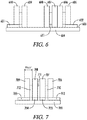
- two adjacent sub-mounts touch as is illustrated in FIG. 6 .
- the pitch is the sum of the thicknesses of two sub-mounts and the laser diode chip.
- two adjacent sub-mounts almost touch and may be connected through a connecting material, not being the laser diode chip.
- the pitch is the sum of the thicknesses of two sub-mounts, any material that may be between the adjacent and almost touching sub-mounts, and the laser diode chip.
- a laser diode or laser source or laser diode chip is typically 100 ⁇ m thick, and the sub-mount thickness may vary from 0.3 mm to 0.8mm.
- the pitch may be as small as 0.4 mm and as large as 2 mm. Numbers outside this range are also possible.
- a pitch is .2 mm or larger. In another embodiment of the present invention the pitch is greater than 2 mm but smaller than 3 mm.
- a distance between the laser diode chip and the carrier is expressed in terms of "half pitch.” This is intended to allow efficient heat dissipation of 45° or about 45° radiation angles from an active area of the laser diode chip via sub-mounts on both sides to the carrier, which acts as a cooler, as illustrated in FIG. 14A and FIG. 14B .
- FIG. 14A and FIG. 14B illustrate examples of embodiments of the present invention. In particular, orientations and dimensions are illustrated.
- the assembly contains a plurality of laser diode chips of which 1402 is identified.
- the laser diode chip 1402 is sandwiched between two sub-mounts 1411 and 1412.
- Sub-mounts 1409 and 1410 sandwich a different laser diode chip.
- FIG. 14A there are two sub-mounts between neighboring laser diode chips.
- the pitch of this structure is thus based on two adjacent sub-mounts and is identified as arrow 1413.
- Each laser diode chip has an active area or region identified as area 1403 in laser diode chip 1402.
- the active area 1403 is the emitting area of 1402.
- the laser diode chips sandwiched between sub-mounts are mounted in a vertical orientation upon carrier 1401.
- the width 1425 of an active area 1403 is also identified as the dimension between the top and the bottom of the active area 1403.
- a laser diode chip has a top relative to the carrier, identified as 1407 and a bottom identified as 1406.
- An active area or region of a laser diode chip has a top of the active area, the top of the active area being identified as 1404 and a bottom of an active area identified as 1405.
- the distance between 1404 and 1405 is the width of the active area.
- a distance from the top 1404 to the carrier 1401 is identified as 1414.
- the distance 1414 is not greater than half the pitch between two neighboring diode laser chips or at least half of 1413.
- a distance between two adjacent diode laser chips in an assembly is determined by a common sub-mount shared by the two adjacent diode laser chips. Accordingly, a pitch between two diode laser chip depends on the combined size of intervening sub-mounts, which may be one sub-mount as in FIG. 14B or two sub-mounts as in FIG. 14A .
- the laser diode chips in an embodiment of the present invention are mounted on opposing sides of a single sub-mount.
- the pitch is defined by arrow 1415 and the minimum distance 1416 of the top of the laser diode chip to the carrier 1401 is not greater than half of 1415.
- a laser diode chip or laser source as shown in FIG. 14A may have dimensions of about 100 micron in the horizontal direction and between 400-600 micron in the vertical direction.
- the active area herein is typically about 100 micron in the vertical direction and several microns in the horizontal direction.
- the sub-mounts may vary in thickness between 0.3 mm to .8 mm or other ranges. Preferably the sub-mounts have a height that allows manipulation, so preferably they should not be too small. All measurements related to the dimensions of features may vary with 10% in accordance with one embodiment of the present invention or up to 25% in accordance with another embodiment of the present invention.
- the top of the active area of the laser diode chip captured or sandwiched between two sub-mounts is positioned at a distance of between about 0.2 mm and 1 mm from the top of the carrier, this distance being determined from the half pitch for laser diode chips in a vertical stack sandwiched between sub-mounts, as defined earlier above.
- Another way to describe a preferred position or height of the laser diode relative to the carrier is to apply a line drawn from the top of the active area of the laser source in a vertical cross-sectional view that is perpendicular to the light-emitting area of the laser source, down through the sub-mount downwards to the carrier under a defined angle between the drawn line and a line perpendicular to the carrier, wherein an angle of about 45° would make the line cross into the carrier directly from the sub-mount. If the sub-mounts that sandwich the laser source have different thicknesses, both of the sandwiching sub-mounts should agree with the 45° rule.
- a line measured under 45° with a line perpendicular to the carrier base and that is measured from the top of the active area of the laser diode chip will cross through the sub-mount of the laser diode chip but not through the sub-mount that is adjacent to the sub-mount of the laser diode chip.
- the 45° may be set in one embodiment of the present invention to be 45° plus or minus 5°.
- the angle rule may be set to be 45° plus or minus 10°.
- the solder layer thickness for vertical stacking is optimized to reduce or eliminate such artifacts and get the bottom of the laser source even closer to the carrier to 50 micron. It may be possible to get as close as 10 micron to the carrier, but the manufacturing margins will be very tight, requiring expensive manufacturing efforts.
- the thermal gain from moving from a 50 micron gap to a 10 micron gap may not be significant enough in many applications to warrant the additional costs. In some embodiments of the present invention, thermal advantages of moving to a 10 micron gap, however small, may be sufficient for those embodiments to warrant the additional manufacturing cost.
- the distance of the center of emitters or multiple emitters to the mounting plane or carrier in a vertically stacked arrangement is precisely aligned such that the deviation from the median center line is preferably 1/10 of the emitter width or less. This helps reduce the overall beam size when all the laser beams are combined, therefore improving the overall beam quality. If the sub-mount side edge and laser diode chip side edge are close enough, both edges could be identified under one microscope view field, making precision alignment easier to achieve. For bonding tools with very precise motors for translation, achieving an alignment accuracy of 5-10 micron is not a problem even if the machine has to identify the two edges separately.
- the carrier 401 hosts at least between 5 and 10 laser diode chips in a single assembly.
- one laser diode chip is attached on either side to sub-mounts 402 and 404.
- Electrical current is provided via patches 405 and 406.
- the desired laser radiation is identified by the arrows 407. It is further noted that optics, such as collimators, will be applied but are omitted from FIG. 4 .
- a laser diode assembly 500 shown in FIG. 5
- radiation from the emitting surface of each laser diode chip is transmitted through a collimating lens 511 and is emitted in a direction parallel to the surface of the carrier base 401.
- Other optics can be used with the laser module of the present invention.
- each of the plurality of sub-mounts are indirectly attached to a conductive pad 501, 502 or 503.
- the sub-mounts 505 and 507 are conductive sub-mounts.
- Each successive pair of the plurality of conductive sub-mounts (e.g. 507 and 512) between a first and a last of the plurality of conductive sub-mounts have a mounting surface attached to one of the plurality of conductive pads (e.g. 502).
- each one of the plurality of laser diode chip has a dimensional length that is greater than a dimensional width that is greater than a dimensional thickness.
- the radiation surface of each laser diode chip is an area defined by the dimensional thickness and the dimensional width.
- the bonding surfaces of each laser diode chip are areas defined by the dimensional length and the dimensional width.
- the first and second open surface of each laser diode chip are areas defined by the dimensional length and the dimensional thickness, and are the top and bottom surfaces of each laser diode chip shown in FIG. 5 .
- each one of the plurality of laser diode chips has a first bonding surface conductively attached to one of the plurality of conductive sub-mounts attached to a first of the conductive pads and has a second bonding surface conductively attached to a second of the plurality of conductive sub-mounts and when radiation is emitted from the radiation surface it is emitted parallel to a surface of the carrier base.
- a first bonding surface of the laser diode 506 is bonded to sub-mount 505 and a second bonding surface of the laser diode 506, on the side opposite the first bonding surface, is bonded to sub-mount 507.
- the first open surface of each one of the plurality of laser sources (i.e. the bottom surface facing the carrier 401) is closer to the surface of the carrier 401 than the second open surface which is on the top of the laser diode 506, opposite the first open surface.
- a gap between the first open surface of each one of the plurality of laser diodes 506 and the surface of the carrier base 401 is less than a predetermined distance, as described and claimed herein.
- the carrier 401 includes a plurality of conductive pads 501, 502 and 503 attached to the surface of the carrier base 401 in a row with a space between adjacent conductive pads.
- the pads 501, 502 and 503 are electrically isolated from each other.
- the pads provide electrical current to the sub-mounts, for instance sub-mounts 505 and 507, when the sub-mounts are made of an electrically conducting material, such as copper-tungsten (CuW).
- CuW copper-tungsten
- the side view of FIG. 5 illustrates part of what a viewer looking into the side of the assembly from where the radiation is coming would see.
- Sub-mounts 505 and 507 sandwich the laser diode chip 506.
- a collimator 511 is not shown with laser diode 506. It is understood that a collimator is present at the output of each laser diode 506.
- the sub-mounts are mounted on electrically conducting pads 501, 502 and 503 in a conventional manner which are used to provide electrical current. The whole assembly sits on carrier 401. One may optimally keep a distance 508 between two sub-mounts sitting on the same pad. This allows optimal alignment of the components on the carrier. However, the sub-mounts may also touch without a space.
- the first open surface (i.e., the bottom surface facing the carrier 401) of each one of the plurality of laser sources 506 is closer to the surface of the carrier than the second open surface (i.e. the top surface) of the laser diode 506 into the top surface 512 of the sub-mounts 505 and 507.
- the space 510 is less than the space 513.
- the space 510 from the carrier to the laser diode is fifty (50%) percent of the size of the distance 513.
- the sub-mounts all have the same dimensions or size. This is, for instance, illustrated in FIGS. 4 and 5 .
- a thickness of each one of the plurality of sub-mounts is in one embodiment of the present invention is between .5 and 1 mm.
- a laser diode 506 formed by a laser diode chip mounted between two sub-mounts can be tested individually before being mounted on the subcarrier. This prevents the installation of a faulty laser diode on a carrier 401 which would be a costly mistake that results in the waste of time and parts.
- each combination of sub-mounts and laser diode chip is individually tested for laser emission before being mounted on the carrier base 401.
- each of the plurality of sub-mounts have a free surface 513 opposing a surface attached to the carrier base 401that is not attached to another carrier. This is illustrated in FIGS. 4 and 5 .
- a free (upper) surface is maintained and the extra cost of mounting a carrier are prevented by providing cooling or heatsink capabilities through the carrier base 401 and by mounting the laser diode chips near the carrier base 401.
- a distance of each of the plurality of laser sources to the free surface is between 10 micron and 800 micron, depending on size of sub-mounts and laser source. While a short gap is maintained from a laser diode chip 506 to the carrier 401, there are benefits to maintain a larger distance 513. This is believed to allow for improved handling of individual laser diodes and for smile management. In one aspect of the present invention, a minimum of distance 513 of each of the plurality of laser sources 506 to the free surface of the sub-mounts is greater than 50 percent of the distance of gap 510 between the laser source 506 and the carrier 401.
- each laser diode chip is bonded to two of the plurality of sub-mounts that are not bonded with another laser source. This is illustrated in for instance FIGS. 4 and 5 .
- each laser diode chip (such as 407 and 506) is bonded to a set of sub-mounts unique to a specific laser diode chip.
- diode 506 is bonded to sub-mounts 505 and 507, and sub-mounts 505 and 507 are not bonded to any other laser diode chip.
- Excitation current that causes the diodes to generate radiation flows from a conductive pad 501 and up through the conductive sub-mount mounted to the pad 501. Electric current then flows through the laser diode (shown with the collimating lens 511) and through the conductive sub-mount leaving surface 512. The current then flows through the conductive pad 502, through the sub-mount 507, through the laser diode 506, through the sub-mount 505 and through the conductor pad 503. Each successive laser diode 506 is excited in this manner, causing the emission of radiation.
- the assembly includes conductive pads 601 and 602, attached to the surface 603 of the carrier base 604 in a row.
- Laser diodes 611 are mounted between each pair of sub-mounts.
- the sub-mounts are conductive sub-mounts with a mounting surface.
- Conductive sub-mounts 610 and 605 mounted to conductive pads 601 and 602, respectively.
- Each adjacent sub-mount between sub-mounts 605 and 610, including 606, 607, 608 and 609, is electrically connected to conduct current. This means that the current flows through the sub-mounts and laser diode chips in the intermediate units, and only the bookend sub-mounts 605 and 610 are connected to conductor pads.
- FIG. 7 illustrates an embodiment similar to FIG.5 , but with adjacent sub-mount pairs (e.g., 507 and 512) replaced with a single sub-mount 707.
- conductive pads 702 to 705 are mounted on a carrier 701.
- single sub-mounts 706 to 709 are mounted on pads 702 to 705, respectively.
- Each laser diode chip 710, 711 and 712 is mounted between the single sub-mounts.
- the embodiment of FIG. 6 can be similarly modified so that each pair of adjacent sub-mounts is replaced with a single sub-mount.
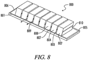
- FIG. 8 illustrates another embodiment of the assembly 800 of the present invention.
- the sub-mounts 802, 804 and 808 can be conductive or non-conductive and are mounted on carrier 801. If non-conductive, the sub-mounts have conductive layers wrapped around from one side to another. Thus, the sub-mounts can be made from a ceramic, such as AlN.
- laser sources 803 and 807 are mounted between sub-mounts 802, 804 and 808 such that a single sub-mount is between each laser source.
- Sub-mount 802 is an end sub-mount that may be connected to a connection pad 805 via a conductive layer 810 that partially or totally covers sub-mount 802.
- the conductive layer 810 can be U-shaped so that it covers both sides of a sub-mount, as well as the bottom of the sub-mount. Thus, in FIG. 8 , the conductive layer 810 wraps around the bottom of the sub-mount 802. Each sub-mount has conductive layer 810 similarly attached to it.
- the arrow 809 extending from one of the laser diodes indicates that the side surfaces are the desired emitting surfaces.
- connection of the sub-mount 802 to the conductive layer 810 is conventional.
- these components can be plated, have thick film or have thin film conductive layers.
- connection of the conductive layer 810 to the carrier 801 is also conventional. For example, it can be attached with solder or thermally conductive adhesive.
- FIG. 8 is further illustrated in FIGS. 9A and 9B .
- Assembly 850 with a carrier 851 is shown in FIG. 9A .
- the laser diode chips 854 and 857 are shown. Each laser diode chip has a gap 858 between a lower open surface and the carrier 851.
- the sub-mounts 853 and 855 are covered with separate conductive layers 852 and 856. It is clearly shown that laser diode chip 854 has adjacent sub-mounts 855 and 853 and that sub-mount 855 is conductively bonded to laser diode chips 857 and 854 and the intermediate conductive layers. One can also see that the sub-mounts are partially covered with a conductive layer. For instance sub-mount 855 is only partially covered with conductive layer 856.
- the covered sub-mounts may for instance be bonded to carrier 851 by adhesive bonding.
- an assembly 860 similar to 850, is illustrated in FIG. 9B .
- the sub-mounts, which may be partially covered, are bonded to the carrier 851 by solder pads, identified as 861, 862 and 863.
- the sub-mounts are preferably made of a ceramic or other electrically insulating material.
- the carrier 801 also is made of a ceramic or electrically insulating material or at least electrically insulates the conductive layers around the sub-mounts from each other.
- the embodiments of the present invention allow for a very compact realization of the assembly.
- the assembly has eight laser diode chips and has a volume not greater than 20x30x10 mm 3 .
- the volume of the assembly includes the total height of the assembly and the size of the carrier.
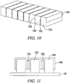
- FIGS. 10 and 11 illustrate another embodiment of the present invention. It shows a configuration of the earlier discussed single shared sub-mounts.
- sub-mount 1203 is shared by laser diode chips 1205 and 1202.
- the sub-mount 1201 has a conductive layer 1204 with covers partially the side, the top and the other side surface of the sub-mounts.
- Each sub-mount has such a layer that can provide electrical current to the assembly of laser diodes.
- the assembly of FIG. 10 is somewhat like the one illustrated in FIG. 8 but upside-down, so that the partially covering conductive layer covers at least a part of the top surface of a sub-mount. This is illustrated in FIG. 11 wherein carrier 1301 is at the opposite side of a covered surface.
- the sub-mount is preferably electrically non-conductive.
- a laser assembly in accordance with the present invention can include eight, or even more laser diode chips. As shown in FIGS. 12 and 13 , one, two or more of the laser assemblies can be mounted on a carrier. In FIG. 12 , a first plurality of vertically oriented laser sources 1601 and a second plurality of vertically oriented laser sources 1602 are mounted on a carrier 1354.
- a sample optical design 1600 to couple the output of the two laser assemblies 1601 and 1602 is shown in FIG. 13 .
- the outputs from the two laser assemblies 1601 and 1602 are reflected with mirrors 1603 and 1604, respectively to an optical combiner 1605 and then into an optical fiber 1606.
- embodiments of the present invention provide very compact platforms for high-power, high-brightness diode laser modules based on single emitters.
- Related modules in the market typically has a dimension of 40x80x15mm 3 ; modules as small as 20x30x10mm 3 may be possible in accordance with various aspects of the present invention.
- aspects of the present invention enable the ability to cool laser diode chips from both P-side and N-side, which may reduce the thermal lensing effect that limits the laser beam quality at high current levels.
- embodiments of the present invention may also reduce the complexity of the whole module and result in a more robust package.
- aspects of the present invention offer the extra advantage that individual CoS sub-assembly can be tested and sorted out before further packaging, thus improving performance and yield of the final product.
- the emitting areas of the laser diode chips assembled in one embodiment of the present invention are all aligned such that a single lens can be used for slow axis collimation. Therefore the emitting areas are aligned to each other such that the total width of all emitting areas in a stack is no larger than 110% of the width of an individual emitting area and that all emitting surfaces are aligned in one plane perpendicular to the beam propagation.
- FIG. 15A and FIG. 15B The numerals in these figures have the same meaning as provided in earlier provided FIG. 1 .
- Numerals 1501, 1502 and 1503 indicate the emitter or active areas of sandwiched laser diode chips.
- the lines 1504 and 1505 illustrate the highest and the lowest height of the active areas of the plurality of sandwiched laser diode chips that are part of the assembly, relative to the carrier 102.
- the lines 1504 and 1505 determine the actual width or effective width of the laser radiation exiting the assembly perpendicular to the emitting areas. One can see that the width of the exit radiation is determined by the variation in the positioning of the laser diode chips and their radiating emitting or active areas.
- the active layers 1509, 1510 and 1514 each of which ends in the active area of the respective diode laser chip, are depicted as dotted lines in FIG. 15B , as they would not be visible in the above view of FIG. 15B .
- the highest position of a top of any of the radiating or emitting areas and the lowest position of any of the radiating or active areas of the laser diode chips that are part of the assembly and which determines the width of the combined exit radiation of the assembly is within 10 % of the width of the radiation of the laser diode chip with the smallest radiation width at the point of exit. This can be achieved at a reasonable effort and cost.
- the 10% variation is determined from the width of the exit radiation of the laser diode chip with the largest radiation width. In general and for practical purposes the width of active areas of the laser diode chips are practically identical.
- the variation of the width of the combined radiation of the active areas is not greater than 20% of the radiation width of the laser diode chip with the smallest radiation width.
- the individual laser diode chips are made within very tight tolerances and may be considered to be identical. In that case the variation is within 10% or 20% of the size of the radiation width of a standard laser diode chip.
- the active areas of the laser diode chips assembled in one embodiment of the present invention are all aligned such that a prefabricated single micro-lens array can be used for fast axis collimation. Therefore the active areas of the individual laser diode chips and the maximum offset of the active area of two laser diode chips that are aligned in a plane perpendicular to the beam propagation direction is not greater than 1 ⁇ m.
- the pitch of the laser diode chips is preferably aligned with an accuracy of better than 1 ⁇ m.
- FIG. 15B provides a top view of the assembly.
- Line 1507 shows a desired position of a sub-mounted laser diode chip and 1508 illustrates a variation of a position of a sandwiched laser diode chip relative to the line1507.
- the laser diode chips are all aligned in a flush manner with sub-mounts.
- FIG. 15B thus illustrates a variation or offset in positioning of the sub-mounts relative to each other and consequently a different relative position of the layers 1509, 1510 and 1514 which are the active layers corresponding to emitting active areas 1501, 1502 and 1503 in FIG. 15A .
- the active areas are the end surfaces of the active layers of the laser diode chips and output the laser radiation of the laser diode chips.
- Another way to define the deviation in alignment of diode laser chips in the direction of radiation is to determine for each diode laser chip a plane through the active area, which is an end surface, perpendicular to radiation propagation from the active area and perpendicular to the carrier. This would be a plane in the plane of the image provided in FIG. 15A or parallel to that plane.
- all these planes coincide into a single plane indicating that all active areas are aligned in one plane.
- some misalignment or offset may occur.
- careful placement and checking for alignment one can assure that the maximum alignment error or offset between active areas is never more than 1 micron or is less than 1 micron or micrometer. This misalignment if called the offset between the active areas of the laser diode chips in an assembly.
Landscapes
- Physics & Mathematics (AREA)
- General Physics & Mathematics (AREA)
- Optics & Photonics (AREA)
- Condensed Matter Physics & Semiconductors (AREA)
- Electromagnetism (AREA)
- Semiconductor Lasers (AREA)
Claims (17)
- Laserdiodenanordnung, umfassend:eine Trägerbasis (1401) mit einer Oberfläche;eine Mehrzahl von Submounts (1409, 1410, 1411, 1412, 853, 855), wobei jeder Submount in der Mehrzahl von Submounts direkt oder indirekt an der Oberfläche der Trägerbasis (1401, 851) befestigt ist; undeine Mehrzahl von Laserdiodenchips (1402, 854, 857), wobei jeder der Mehrzahl von Laserdiodenchips (1402, 854, 857) zwei gegenüberliegende Verbindungsflächen und eine aktive Schicht zwischen den zwei Verbindungsflächen hat, wobei die Verbindungsflächen und die aktive Schicht senkrecht zur Oberfläche der Trägerbasis sind und jede der zwei gegenüberliegenden Verbindungsflächen an einem der Mehrzahl von Submounts (1409, 1410, 1411, 1412, 853, 855) befestigt ist, so dass jeder der Mehrzahl von Laserdiodenchips (1402, 854, 857) einschließlich der aktiven Schicht vertikal bezüglich der Trägerbasis (1401, 851) ausgerichtet ist, wobei jeder Laserdiodenchip (1402, 854, 857) einen aktiven Bereich (1403) am Ende der aktiven Schicht hat, mit einer oberen Fläche bezüglich der Trägerbasis, die bei Antrieb mit elektrischem Strom Strahlung parallel zu der Oberfläche der Trägerbasis (1401, 854, 857) aussenden kann;dadurch gekennzeichnet, dass
ein Abstand (1414, 1416) zwischen der oberen Fläche des aktiven Bereichs jedes der Mehrzahl von Laserdiodenchips und der Trägerbasis nicht größer als der halbe Pitch (1413, 1415), plus oder minus 10%, zwischen benachbarten Laserdiodenchips der Mehrzahl von Laserdiodenchips (1402, 854, 857) in der Laserdiodenanordnung ist. - Anordnung nach Anspruch 1, wobei der Abstand zwischen der oberen Fläche des aktiven Bereichs jedes Laserdiodenchips in der Mehrzahl von Laserdiodenchips und der Trägerbasis zwischen 0,2mm und 1mm beträgt.
- Laserdiodenanordnung nach Anspruch 1, wobei ein Abstand zwischen einer Unterseite jedes Laserdiodenchips in der Mehrzahl von Laserdiodenchips und der Trägerbasis in der Laserdiodenanordnung kleiner als 50 Mikrometer ist.
- Laserdiodenanordnung nach Anspruch 1, wobei ein Abstand eines Mittelpunkts des aktiven Bereichs jedes Laserdiodenchips in der Mehrzahl von Laserdiodenchips von einer Median-Mittellinie durch die aktiven Bereiche der Laserdiodenchips in der Mehrzahl von Laserdiodenchips nicht größer als 1/10 einer Breite des aktiven Bereichs eines beliebigen der Laserdiodenchips ist.
- Laserdiodenanordnung nach Anspruch 1, wobei jeder aktive Bereich eines Laserdiodenchips in der Mehrzahl von Laserdiodenchips eine Ebene senkrecht zur Strahlung von dem aktiven Bereich und senkrecht zu dem Träger festlegt, um eine Mehrzahl von im Wesentlichen parallelen Ebenen zu bilden, und ein Abstand zwischen zwei beliebigen Ebenen in der Mehrzahl von Ebenen nicht größer als 1 Mikrometer ist.
- Laserdiodenanordnung nach Anspruch 1, weiter umfassend: eine einzige Kollimationslinse, um Laserstrahlung entlang der langsamen Achse der Laserdiodenanordnung zu kollimieren.
- Laserdiodenanordnung nach Anspruch 1, weiter umfassend:eine Mehrzahl von leitenden Anschluss-Pads (501, 502, 503), die an der Oberfläche der Trägerbasis (401) in einer Reihe mit einem Raum (510) zwischen angrenzenden leitenden Anschluss-Pads befestigt ist;wobei die Submounts leitende Submounts sind, wobei jedes der Mehrzahl von leitenden Submounts eine Montagefläche hat, die an einer der Mehrzahl von leitenden Anschluss-Pads befestigt ist; undjeder der Mehrzahl von Laserdiodenchips an einem leitenden Submount in einer Position oberhalb des Raums zwischen angrenzenden leitenden Anschluss-Pads befestigt ist.
- Laserdiodenanordnung nach Anspruch 7, wobei jeder der Mehrzahl von Submounts dieselbe Größe hat.
- Laserdiodenanordnung nach Anspruch 7, wobei eine Dicke jedes der Mehrzahl von Submounts zwischen 0,3 und 0,8mm beträgt.
- Laserdiodenanordnung nach Anspruch 5, weiter umfassend:ein vorgefertigtes Mikrolinsen-Array zur Fast-Axis-Kollimation von Strahlung, die von der Mehrzahl der Laserdiodenchips erzeugt wird.
- Laserdiodenanordnung nach Anspruch 1, wobei die Anordnung mehr als 5 Laserdiodenchips hat und einen Bereich von nicht mehr als 20mm x 10mm einnimmt.
- Laserdiodenanordnung nach Anspruch 1, wobei jeder der Mehrzahl von Submounts (853, 855) aus einem keramischen Material gefertigt ist, das zumindest teilweise mit einer Schicht aus leitendem Material (852, 856) auf einer ersten Seite und einer zweiten Seite bedeckt ist, die jeweils an einem anderen Laserdiodenchip (854, 857) zu befestigen sind.
- Laserdiodenanordnung nach Anspruch 12, wobei jeder der Laserdiodenchips (854, 857) eine erste und eine zweite Befestigungsseite hat, wobei jede der ersten und zweiten Befestigungsseiten der Mehrzahl von Laserdiodenchips (854, 857) an der Schicht aus leitendem Material (852, 856) eines anderen Submounts in der Mehrzahl von Submounts (853, 855) befestigt und elektrisch verbunden ist.
- Laserdiodenanordnung nach Anspruch 13, wobei das leitende Material einen Abschnitt jeder Seite jedes Submounts bedeckt und ebenfalls mindestens Teil einer unteren Montagefläche jedes Submounts, das an der Trägerbasis befestigt werden soll, bedeckt.
- Laserdiodenanordnung nach Anspruch 13, wobei das leitende Material einen Abschnitt jeder Seite jedes Montageelements bedeckt und ebenfalls mindestens eine obere Fläche jedes Submounts bedeckt, der nicht an der Trägerbasis befestigt ist.
- Laserdiodenanordnung nach Anspruch 13, wobei ein Abstand eines Mittelpunkts des aktiven Bereichs jedes Laserdiodenchips in der Laseranordnung von einer Median-Mittellinie durch die aktiven Bereiche der Laserdiodenchips in der Laserdiodenanordnung nicht größer als 1/10 einer Breite eines breitesten aktiven Bereichs eines beliebigen der Laserdiodenchips in der Laserdiodenanordnung ist.
- Laserdiodenanordnung nach Anspruch 13, wobei die Laserdiodenanordnung mehr als 5 und bis zu 10 Laserdiodenchips innerhalb eines Flächenbereichs der Trägerbasis von nicht mehr als 20x10mm2 hat.
Applications Claiming Priority (2)
| Application Number | Priority Date | Filing Date | Title |
|---|---|---|---|
| US14/702,852 US9450377B1 (en) | 2015-05-04 | 2015-05-04 | Multi-emitter diode laser package |
| PCT/US2016/030687 WO2016179229A1 (en) | 2015-05-04 | 2016-05-04 | Multi-emitter diode laser package |
Publications (2)
| Publication Number | Publication Date |
|---|---|
| EP3292598A1 EP3292598A1 (de) | 2018-03-14 |
| EP3292598B1 true EP3292598B1 (de) | 2019-02-27 |
Family
ID=55963496
Family Applications (1)
| Application Number | Title | Priority Date | Filing Date |
|---|---|---|---|
| EP16722028.4A Active EP3292598B1 (de) | 2015-05-04 | 2016-05-04 | Multi-emitter-diodenlaserbaugruppe |
Country Status (4)
| Country | Link |
|---|---|
| US (1) | US9450377B1 (de) |
| EP (1) | EP3292598B1 (de) |
| CN (1) | CN107743592B (de) |
| WO (1) | WO2016179229A1 (de) |
Families Citing this family (24)
| Publication number | Priority date | Publication date | Assignee | Title |
|---|---|---|---|---|
| DE102013216527A1 (de) * | 2013-08-21 | 2015-02-26 | Osram Opto Semiconductors Gmbh | Laserbauelement und Verfahren zum Herstellen eines Laserbauelements |
| US10297976B2 (en) * | 2015-05-19 | 2019-05-21 | Ii-Vi Laser Enterprise Gmbh | Low thermal resistance, stress-controlled diode laser assemblies |
| JP6631502B2 (ja) | 2016-12-27 | 2020-01-15 | 日亜化学工業株式会社 | レーザパッケージの製造方法 |
| JP7080971B2 (ja) | 2017-11-01 | 2022-06-06 | ヌブル インク | マルチkWクラスの青色レーザーシステム |
| EP3710859B1 (de) | 2018-04-28 | 2023-04-19 | SZ DJI Technology Co., Ltd. | Lichtdetektions- und entfernungsmesssensoren mit mehreren emittern und mehreren empfängern sowie zugehörige systeme und verfahren |
| WO2019205163A1 (en) * | 2018-04-28 | 2019-10-31 | SZ DJI Technology Co., Ltd. | Light detection and ranging sensors with multiple emitters and multiple receivers, and associated systems and methods |
| JP7152652B2 (ja) * | 2018-06-13 | 2022-10-13 | 日亜化学工業株式会社 | 光源装置 |
| NL2022241B1 (en) | 2018-12-18 | 2020-07-03 | Sencio B V | Laser chip package |
| CN110544871B (zh) * | 2019-08-29 | 2024-07-05 | 西安炬光科技股份有限公司 | 半导体激光器的封装结构及叠阵结构 |
| CN110518453A (zh) * | 2019-09-27 | 2019-11-29 | 石家庄麦特达电子科技有限公司 | 半导体激光器阵列的封装结构 |
| US20220360039A1 (en) * | 2019-09-30 | 2022-11-10 | Osram Opto Semiconductors Gmbh | Laser package and system with laser packages |
| JP7417045B2 (ja) * | 2019-10-23 | 2024-01-18 | 日亜化学工業株式会社 | 光源装置 |
| CN111029894A (zh) * | 2019-12-27 | 2020-04-17 | 海特光电有限责任公司 | 一种半导体激光器及其封装方法 |
| CN111193179B (zh) * | 2020-03-06 | 2025-06-06 | 西安炬光科技股份有限公司 | 激光叠阵 |
| DE102020118421B4 (de) * | 2020-07-13 | 2023-08-03 | Focuslight Technologies Inc. | Laservorrichtung |
| US11557874B2 (en) * | 2021-05-18 | 2023-01-17 | Trumpf Photonics, Inc. | Double-sided cooling of laser diodes |
| US11876343B2 (en) | 2021-05-18 | 2024-01-16 | Trumpf Photonics, Inc. | Laser diode packaging platforms |
| WO2023089059A2 (en) * | 2021-11-19 | 2023-05-25 | Ams-Osram International Gmbh | Laser package and method for manufacturing a laser package |
| CN114649741A (zh) * | 2022-03-23 | 2022-06-21 | 西安欧益光电科技有限公司 | 一种新型大功率叠阵激光器封装工艺及工装 |
| DE102022106938A1 (de) | 2022-03-24 | 2023-09-28 | Ams-Osram International Gmbh | Gestapelte laseranordnung und verfahren zum erzeugen derselben |
| CN115296139B (zh) * | 2022-10-11 | 2022-12-30 | 昆山三智达自动化设备科技有限公司 | 基于模块化底座的cos组装方法及组装设备 |
| CN115764552B (zh) * | 2022-10-27 | 2025-08-08 | 中国电子科技集团公司第十三研究所 | 准连续阵列激光泵源及其制备方法 |
| DE102023124035A1 (de) | 2023-09-06 | 2025-03-06 | Jenoptik Optical Systems Gmbh | Verfahren zur Herstellung eines Laserdiodenmoduls sowie Mehrlagensubstrat und Laserverbund zur Verwendung in einem Verfahren zur Herstellung eines Laserdiodenmoduls |
| DE102023133711A1 (de) * | 2023-12-01 | 2025-06-05 | TRUMPF Laser SE | Laseremitter-Anordnung |
Family Cites Families (13)
| Publication number | Priority date | Publication date | Assignee | Title |
|---|---|---|---|---|
| RU2117371C1 (ru) * | 1996-09-30 | 1998-08-10 | Акционерное общество закрытого типа "Энергомаштехника" | Матрица лазерных диодов |
| US6295307B1 (en) * | 1997-10-14 | 2001-09-25 | Decade Products, Inc. | Laser diode assembly |
| US6424667B1 (en) * | 1998-12-04 | 2002-07-23 | Jds Uniphase Corporation | Solder and material designs to improve resistance to cycling fatigue in laser diode stacks |
| EP1811617A1 (de) * | 2006-01-18 | 2007-07-25 | JENOPTIK Laserdiode GmbH | Träger für eine vertikale Anordnung von Laserdiodenbarren mit Anschlag |
| US7515346B2 (en) | 2006-07-18 | 2009-04-07 | Coherent, Inc. | High power and high brightness diode-laser array for material processing applications |
| US8437086B2 (en) | 2010-06-30 | 2013-05-07 | Jds Uniphase Corporation | Beam combining light source |
| US8432945B2 (en) | 2010-09-30 | 2013-04-30 | Victor Faybishenko | Laser diode combiner modules |
| JP5566268B2 (ja) | 2010-11-19 | 2014-08-06 | 新光電気工業株式会社 | 発光装置及びパッケージ部品 |
| EP2477285A1 (de) | 2011-01-18 | 2012-07-18 | Bystronic Laser AG | Laserdiodenbarren und Lasersystem |
| US8804782B2 (en) | 2012-10-29 | 2014-08-12 | Coherent, Inc. | Macro-channel water-cooled heat-sink for diode-laser bars |
| DE102013224420A1 (de) * | 2013-05-13 | 2014-11-13 | Osram Gmbh | Laserbauelement und Verfahren zur seiner Herstellung |
| JP2015153842A (ja) | 2014-02-13 | 2015-08-24 | 三菱電機株式会社 | 半導体レーザ光源 |
| US9054482B1 (en) | 2014-05-07 | 2015-06-09 | Jiang Li | Laser diode stack assembly and method of manufacturing |
-
2015
- 2015-05-04 US US14/702,852 patent/US9450377B1/en active Active
-
2016
- 2016-05-04 EP EP16722028.4A patent/EP3292598B1/de active Active
- 2016-05-04 CN CN201680026067.XA patent/CN107743592B/zh active Active
- 2016-05-04 WO PCT/US2016/030687 patent/WO2016179229A1/en not_active Ceased
Non-Patent Citations (1)
| Title |
|---|
| None * |
Also Published As
| Publication number | Publication date |
|---|---|
| CN107743592B (zh) | 2019-08-13 |
| WO2016179229A1 (en) | 2016-11-10 |
| CN107743592A (zh) | 2018-02-27 |
| US9450377B1 (en) | 2016-09-20 |
| EP3292598A1 (de) | 2018-03-14 |
Similar Documents
| Publication | Publication Date | Title |
|---|---|---|
| EP3292598B1 (de) | Multi-emitter-diodenlaserbaugruppe | |
| US7420996B2 (en) | Modular diode laser assembly | |
| US7848372B2 (en) | Modular diode laser assembly | |
| US7436868B2 (en) | Modular diode laser assembly | |
| US7801190B2 (en) | Carrier for a vertical arrangement of laser diodes with a stop | |
| CN107851963B (zh) | 具有冷却结构的阶梯式二极管激光模块 | |
| US7443895B2 (en) | Modular diode laser assembly | |
| EP1788676B1 (de) | Modulare Anordnung verwendend Laserdiodenbaugruppen mit Montageblöcken mit Flügeln | |
| US7586963B2 (en) | Modular diode laser assembly | |
| US5923692A (en) | No wire bond plate (NWBP) packaging architecture for two dimensional stacked diode laser arrays | |
| US10680405B2 (en) | Semiconductor light-emitting device | |
| US11557874B2 (en) | Double-sided cooling of laser diodes | |
| US20070217469A1 (en) | Laser diode stack side-pumped solid state laser | |
| US20070217470A1 (en) | Laser diode stack end-pumped solid state laser | |
| US20070217471A1 (en) | Laser diode stack utilizing a non-conductive submount | |
| US20070217468A1 (en) | Laser diode package utilizing a laser diode stack | |
| US20230283043A1 (en) | High peak power laser diode assembly | |
| KR102669828B1 (ko) | 레이저 다이오드 패키지 | |
| US20190115719A1 (en) | Semiconductor light-emitting element and semiconductor light-emitting device | |
| WO2011129183A1 (ja) | 光伝送モジュールおよびこれを用いた光通信装置 | |
| CN222654555U (zh) | 激光器 | |
| WO2007061509A2 (en) | Modular diode laser assembly | |
| HK40098350A (zh) | 高峰值功率激光二极管组件 | |
| JP2015213109A (ja) | レーザ光源モジュール |
Legal Events
| Date | Code | Title | Description |
|---|---|---|---|
| STAA | Information on the status of an ep patent application or granted ep patent |
Free format text: STATUS: THE INTERNATIONAL PUBLICATION HAS BEEN MADE |
|
| PUAI | Public reference made under article 153(3) epc to a published international application that has entered the european phase |
Free format text: ORIGINAL CODE: 0009012 |
|
| STAA | Information on the status of an ep patent application or granted ep patent |
Free format text: STATUS: REQUEST FOR EXAMINATION WAS MADE |
|
| 17P | Request for examination filed |
Effective date: 20171204 |
|
| AK | Designated contracting states |
Kind code of ref document: A1 Designated state(s): AL AT BE BG CH CY CZ DE DK EE ES FI FR GB GR HR HU IE IS IT LI LT LU LV MC MK MT NL NO PL PT RO RS SE SI SK SM TR |
|
| AX | Request for extension of the european patent |
Extension state: BA ME |
|
| RIN1 | Information on inventor provided before grant (corrected) |
Inventor name: LI, YUFENG Inventor name: TREUSCH, HANS-GEORG Inventor name: ROFF, ROBERT, WALLACE Inventor name: HEINEMANN, STEFAN |
|
| DAV | Request for validation of the european patent (deleted) | ||
| DAX | Request for extension of the european patent (deleted) | ||
| GRAP | Despatch of communication of intention to grant a patent |
Free format text: ORIGINAL CODE: EPIDOSNIGR1 |
|
| STAA | Information on the status of an ep patent application or granted ep patent |
Free format text: STATUS: GRANT OF PATENT IS INTENDED |
|
| INTG | Intention to grant announced |
Effective date: 20180919 |
|
| RAP1 | Party data changed (applicant data changed or rights of an application transferred) |
Owner name: TRUMPF PHOTONICS, INC. |
|
| GRAS | Grant fee paid |
Free format text: ORIGINAL CODE: EPIDOSNIGR3 |
|
| GRAA | (expected) grant |
Free format text: ORIGINAL CODE: 0009210 |
|
| STAA | Information on the status of an ep patent application or granted ep patent |
Free format text: STATUS: THE PATENT HAS BEEN GRANTED |
|
| AK | Designated contracting states |
Kind code of ref document: B1 Designated state(s): AL AT BE BG CH CY CZ DE DK EE ES FI FR GB GR HR HU IE IS IT LI LT LU LV MC MK MT NL NO PL PT RO RS SE SI SK SM TR |
|
| REG | Reference to a national code |
Ref country code: GB Ref legal event code: FG4D |
|
| REG | Reference to a national code |
Ref country code: CH Ref legal event code: EP |
|
| REG | Reference to a national code |
Ref country code: AT Ref legal event code: REF Ref document number: 1102702 Country of ref document: AT Kind code of ref document: T Effective date: 20190315 |
|
| REG | Reference to a national code |
Ref country code: IE Ref legal event code: FG4D |
|
| REG | Reference to a national code |
Ref country code: DE Ref legal event code: R096 Ref document number: 602016010423 Country of ref document: DE |
|
| REG | Reference to a national code |
Ref country code: CH Ref legal event code: NV Representative=s name: DENNEMEYER AG, CH |
|
| REG | Reference to a national code |
Ref country code: NL Ref legal event code: MP Effective date: 20190227 |
|
| REG | Reference to a national code |
Ref country code: LT Ref legal event code: MG4D |
|
| PG25 | Lapsed in a contracting state [announced via postgrant information from national office to epo] |
Ref country code: NO Free format text: LAPSE BECAUSE OF FAILURE TO SUBMIT A TRANSLATION OF THE DESCRIPTION OR TO PAY THE FEE WITHIN THE PRESCRIBED TIME-LIMIT Effective date: 20190527 Ref country code: NL Free format text: LAPSE BECAUSE OF FAILURE TO SUBMIT A TRANSLATION OF THE DESCRIPTION OR TO PAY THE FEE WITHIN THE PRESCRIBED TIME-LIMIT Effective date: 20190227 Ref country code: LT Free format text: LAPSE BECAUSE OF FAILURE TO SUBMIT A TRANSLATION OF THE DESCRIPTION OR TO PAY THE FEE WITHIN THE PRESCRIBED TIME-LIMIT Effective date: 20190227 Ref country code: PT Free format text: LAPSE BECAUSE OF FAILURE TO SUBMIT A TRANSLATION OF THE DESCRIPTION OR TO PAY THE FEE WITHIN THE PRESCRIBED TIME-LIMIT Effective date: 20190627 Ref country code: SE Free format text: LAPSE BECAUSE OF FAILURE TO SUBMIT A TRANSLATION OF THE DESCRIPTION OR TO PAY THE FEE WITHIN THE PRESCRIBED TIME-LIMIT Effective date: 20190227 Ref country code: FI Free format text: LAPSE BECAUSE OF FAILURE TO SUBMIT A TRANSLATION OF THE DESCRIPTION OR TO PAY THE FEE WITHIN THE PRESCRIBED TIME-LIMIT Effective date: 20190227 |
|
| PG25 | Lapsed in a contracting state [announced via postgrant information from national office to epo] |
Ref country code: LV Free format text: LAPSE BECAUSE OF FAILURE TO SUBMIT A TRANSLATION OF THE DESCRIPTION OR TO PAY THE FEE WITHIN THE PRESCRIBED TIME-LIMIT Effective date: 20190227 Ref country code: RS Free format text: LAPSE BECAUSE OF FAILURE TO SUBMIT A TRANSLATION OF THE DESCRIPTION OR TO PAY THE FEE WITHIN THE PRESCRIBED TIME-LIMIT Effective date: 20190227 Ref country code: IS Free format text: LAPSE BECAUSE OF FAILURE TO SUBMIT A TRANSLATION OF THE DESCRIPTION OR TO PAY THE FEE WITHIN THE PRESCRIBED TIME-LIMIT Effective date: 20190627 Ref country code: BG Free format text: LAPSE BECAUSE OF FAILURE TO SUBMIT A TRANSLATION OF THE DESCRIPTION OR TO PAY THE FEE WITHIN THE PRESCRIBED TIME-LIMIT Effective date: 20190527 Ref country code: GR Free format text: LAPSE BECAUSE OF FAILURE TO SUBMIT A TRANSLATION OF THE DESCRIPTION OR TO PAY THE FEE WITHIN THE PRESCRIBED TIME-LIMIT Effective date: 20190528 Ref country code: HR Free format text: LAPSE BECAUSE OF FAILURE TO SUBMIT A TRANSLATION OF THE DESCRIPTION OR TO PAY THE FEE WITHIN THE PRESCRIBED TIME-LIMIT Effective date: 20190227 |
|
| REG | Reference to a national code |
Ref country code: AT Ref legal event code: MK05 Ref document number: 1102702 Country of ref document: AT Kind code of ref document: T Effective date: 20190227 |
|
| PG25 | Lapsed in a contracting state [announced via postgrant information from national office to epo] |
Ref country code: DK Free format text: LAPSE BECAUSE OF FAILURE TO SUBMIT A TRANSLATION OF THE DESCRIPTION OR TO PAY THE FEE WITHIN THE PRESCRIBED TIME-LIMIT Effective date: 20190227 Ref country code: ES Free format text: LAPSE BECAUSE OF FAILURE TO SUBMIT A TRANSLATION OF THE DESCRIPTION OR TO PAY THE FEE WITHIN THE PRESCRIBED TIME-LIMIT Effective date: 20190227 Ref country code: AL Free format text: LAPSE BECAUSE OF FAILURE TO SUBMIT A TRANSLATION OF THE DESCRIPTION OR TO PAY THE FEE WITHIN THE PRESCRIBED TIME-LIMIT Effective date: 20190227 Ref country code: SK Free format text: LAPSE BECAUSE OF FAILURE TO SUBMIT A TRANSLATION OF THE DESCRIPTION OR TO PAY THE FEE WITHIN THE PRESCRIBED TIME-LIMIT Effective date: 20190227 Ref country code: RO Free format text: LAPSE BECAUSE OF FAILURE TO SUBMIT A TRANSLATION OF THE DESCRIPTION OR TO PAY THE FEE WITHIN THE PRESCRIBED TIME-LIMIT Effective date: 20190227 Ref country code: IT Free format text: LAPSE BECAUSE OF FAILURE TO SUBMIT A TRANSLATION OF THE DESCRIPTION OR TO PAY THE FEE WITHIN THE PRESCRIBED TIME-LIMIT Effective date: 20190227 Ref country code: CZ Free format text: LAPSE BECAUSE OF FAILURE TO SUBMIT A TRANSLATION OF THE DESCRIPTION OR TO PAY THE FEE WITHIN THE PRESCRIBED TIME-LIMIT Effective date: 20190227 Ref country code: EE Free format text: LAPSE BECAUSE OF FAILURE TO SUBMIT A TRANSLATION OF THE DESCRIPTION OR TO PAY THE FEE WITHIN THE PRESCRIBED TIME-LIMIT Effective date: 20190227 |
|
| REG | Reference to a national code |
Ref country code: DE Ref legal event code: R097 Ref document number: 602016010423 Country of ref document: DE |
|
| PG25 | Lapsed in a contracting state [announced via postgrant information from national office to epo] |
Ref country code: SM Free format text: LAPSE BECAUSE OF FAILURE TO SUBMIT A TRANSLATION OF THE DESCRIPTION OR TO PAY THE FEE WITHIN THE PRESCRIBED TIME-LIMIT Effective date: 20190227 Ref country code: PL Free format text: LAPSE BECAUSE OF FAILURE TO SUBMIT A TRANSLATION OF THE DESCRIPTION OR TO PAY THE FEE WITHIN THE PRESCRIBED TIME-LIMIT Effective date: 20190227 |
|
| PG25 | Lapsed in a contracting state [announced via postgrant information from national office to epo] |
Ref country code: AT Free format text: LAPSE BECAUSE OF FAILURE TO SUBMIT A TRANSLATION OF THE DESCRIPTION OR TO PAY THE FEE WITHIN THE PRESCRIBED TIME-LIMIT Effective date: 20190227 |
|
| PLBE | No opposition filed within time limit |
Free format text: ORIGINAL CODE: 0009261 |
|
| STAA | Information on the status of an ep patent application or granted ep patent |
Free format text: STATUS: NO OPPOSITION FILED WITHIN TIME LIMIT |
|
| PG25 | Lapsed in a contracting state [announced via postgrant information from national office to epo] |
Ref country code: MC Free format text: LAPSE BECAUSE OF FAILURE TO SUBMIT A TRANSLATION OF THE DESCRIPTION OR TO PAY THE FEE WITHIN THE PRESCRIBED TIME-LIMIT Effective date: 20190227 |
|
| 26N | No opposition filed |
Effective date: 20191128 |
|
| REG | Reference to a national code |
Ref country code: BE Ref legal event code: MM Effective date: 20190531 |
|
| PG25 | Lapsed in a contracting state [announced via postgrant information from national office to epo] |
Ref country code: SI Free format text: LAPSE BECAUSE OF FAILURE TO SUBMIT A TRANSLATION OF THE DESCRIPTION OR TO PAY THE FEE WITHIN THE PRESCRIBED TIME-LIMIT Effective date: 20190227 Ref country code: LU Free format text: LAPSE BECAUSE OF NON-PAYMENT OF DUE FEES Effective date: 20190504 |
|
| PG25 | Lapsed in a contracting state [announced via postgrant information from national office to epo] |
Ref country code: TR Free format text: LAPSE BECAUSE OF FAILURE TO SUBMIT A TRANSLATION OF THE DESCRIPTION OR TO PAY THE FEE WITHIN THE PRESCRIBED TIME-LIMIT Effective date: 20190227 |
|
| PG25 | Lapsed in a contracting state [announced via postgrant information from national office to epo] |
Ref country code: IE Free format text: LAPSE BECAUSE OF NON-PAYMENT OF DUE FEES Effective date: 20190504 |
|
| PG25 | Lapsed in a contracting state [announced via postgrant information from national office to epo] |
Ref country code: BE Free format text: LAPSE BECAUSE OF NON-PAYMENT OF DUE FEES Effective date: 20190531 |
|
| PG25 | Lapsed in a contracting state [announced via postgrant information from national office to epo] |
Ref country code: CY Free format text: LAPSE BECAUSE OF FAILURE TO SUBMIT A TRANSLATION OF THE DESCRIPTION OR TO PAY THE FEE WITHIN THE PRESCRIBED TIME-LIMIT Effective date: 20190227 |
|
| PG25 | Lapsed in a contracting state [announced via postgrant information from national office to epo] |
Ref country code: MT Free format text: LAPSE BECAUSE OF FAILURE TO SUBMIT A TRANSLATION OF THE DESCRIPTION OR TO PAY THE FEE WITHIN THE PRESCRIBED TIME-LIMIT Effective date: 20190227 Ref country code: HU Free format text: LAPSE BECAUSE OF FAILURE TO SUBMIT A TRANSLATION OF THE DESCRIPTION OR TO PAY THE FEE WITHIN THE PRESCRIBED TIME-LIMIT; INVALID AB INITIO Effective date: 20160504 |
|
| PG25 | Lapsed in a contracting state [announced via postgrant information from national office to epo] |
Ref country code: MK Free format text: LAPSE BECAUSE OF FAILURE TO SUBMIT A TRANSLATION OF THE DESCRIPTION OR TO PAY THE FEE WITHIN THE PRESCRIBED TIME-LIMIT Effective date: 20190227 |
|
| PGFP | Annual fee paid to national office [announced via postgrant information from national office to epo] |
Ref country code: DE Payment date: 20250521 Year of fee payment: 10 |
|
| PGFP | Annual fee paid to national office [announced via postgrant information from national office to epo] |
Ref country code: GB Payment date: 20250527 Year of fee payment: 10 |
|
| PGFP | Annual fee paid to national office [announced via postgrant information from national office to epo] |
Ref country code: FR Payment date: 20250528 Year of fee payment: 10 |
|
| PGFP | Annual fee paid to national office [announced via postgrant information from national office to epo] |
Ref country code: CH Payment date: 20250601 Year of fee payment: 10 |