EP3293614A1 - Panneau d'affichage tactile et son procédé de commande, et dispositif d'affichage tactile - Google Patents
Panneau d'affichage tactile et son procédé de commande, et dispositif d'affichage tactile Download PDFInfo
- Publication number
- EP3293614A1 EP3293614A1 EP15866396.3A EP15866396A EP3293614A1 EP 3293614 A1 EP3293614 A1 EP 3293614A1 EP 15866396 A EP15866396 A EP 15866396A EP 3293614 A1 EP3293614 A1 EP 3293614A1
- Authority
- EP
- European Patent Office
- Prior art keywords
- electrodes
- display panel
- touch
- touch display
- electrode
- Prior art date
- Legal status (The legal status is an assumption and is not a legal conclusion. Google has not performed a legal analysis and makes no representation as to the accuracy of the status listed.)
- Granted
Links
Images


Classifications
-
- G—PHYSICS
- G06—COMPUTING OR CALCULATING; COUNTING
- G06F—ELECTRIC DIGITAL DATA PROCESSING
- G06F3/00—Input arrangements for transferring data to be processed into a form capable of being handled by the computer; Output arrangements for transferring data from processing unit to output unit, e.g. interface arrangements
- G06F3/01—Input arrangements or combined input and output arrangements for interaction between user and computer
- G06F3/03—Arrangements for converting the position or the displacement of a member into a coded form
- G06F3/041—Digitisers, e.g. for touch screens or touch pads, characterised by the transducing means
- G06F3/044—Digitisers, e.g. for touch screens or touch pads, characterised by the transducing means by capacitive means
- G06F3/0445—Digitisers, e.g. for touch screens or touch pads, characterised by the transducing means by capacitive means using two or more layers of sensing electrodes, e.g. using two layers of electrodes separated by a dielectric layer
-
- G—PHYSICS
- G06—COMPUTING OR CALCULATING; COUNTING
- G06F—ELECTRIC DIGITAL DATA PROCESSING
- G06F3/00—Input arrangements for transferring data to be processed into a form capable of being handled by the computer; Output arrangements for transferring data from processing unit to output unit, e.g. interface arrangements
- G06F3/01—Input arrangements or combined input and output arrangements for interaction between user and computer
- G06F3/03—Arrangements for converting the position or the displacement of a member into a coded form
- G06F3/041—Digitisers, e.g. for touch screens or touch pads, characterised by the transducing means
- G06F3/0412—Digitisers structurally integrated in a display
-
- G—PHYSICS
- G06—COMPUTING OR CALCULATING; COUNTING
- G06F—ELECTRIC DIGITAL DATA PROCESSING
- G06F3/00—Input arrangements for transferring data to be processed into a form capable of being handled by the computer; Output arrangements for transferring data from processing unit to output unit, e.g. interface arrangements
- G06F3/01—Input arrangements or combined input and output arrangements for interaction between user and computer
- G06F3/03—Arrangements for converting the position or the displacement of a member into a coded form
- G06F3/041—Digitisers, e.g. for touch screens or touch pads, characterised by the transducing means
- G06F3/044—Digitisers, e.g. for touch screens or touch pads, characterised by the transducing means by capacitive means
-
- G—PHYSICS
- G06—COMPUTING OR CALCULATING; COUNTING
- G06F—ELECTRIC DIGITAL DATA PROCESSING
- G06F3/00—Input arrangements for transferring data to be processed into a form capable of being handled by the computer; Output arrangements for transferring data from processing unit to output unit, e.g. interface arrangements
- G06F3/01—Input arrangements or combined input and output arrangements for interaction between user and computer
- G06F3/03—Arrangements for converting the position or the displacement of a member into a coded form
- G06F3/041—Digitisers, e.g. for touch screens or touch pads, characterised by the transducing means
- G06F3/0416—Control or interface arrangements specially adapted for digitisers
-
- G—PHYSICS
- G06—COMPUTING OR CALCULATING; COUNTING
- G06F—ELECTRIC DIGITAL DATA PROCESSING
- G06F3/00—Input arrangements for transferring data to be processed into a form capable of being handled by the computer; Output arrangements for transferring data from processing unit to output unit, e.g. interface arrangements
- G06F3/01—Input arrangements or combined input and output arrangements for interaction between user and computer
- G06F3/03—Arrangements for converting the position or the displacement of a member into a coded form
- G06F3/041—Digitisers, e.g. for touch screens or touch pads, characterised by the transducing means
- G06F3/0416—Control or interface arrangements specially adapted for digitisers
- G06F3/04166—Details of scanning methods, e.g. sampling time, grouping of sub areas or time sharing with display driving
-
- G—PHYSICS
- G06—COMPUTING OR CALCULATING; COUNTING
- G06F—ELECTRIC DIGITAL DATA PROCESSING
- G06F3/00—Input arrangements for transferring data to be processed into a form capable of being handled by the computer; Output arrangements for transferring data from processing unit to output unit, e.g. interface arrangements
- G06F3/01—Input arrangements or combined input and output arrangements for interaction between user and computer
- G06F3/03—Arrangements for converting the position or the displacement of a member into a coded form
- G06F3/041—Digitisers, e.g. for touch screens or touch pads, characterised by the transducing means
- G06F3/0416—Control or interface arrangements specially adapted for digitisers
- G06F3/0418—Control or interface arrangements specially adapted for digitisers for error correction or compensation, e.g. based on parallax, calibration or alignment
-
- G—PHYSICS
- G06—COMPUTING OR CALCULATING; COUNTING
- G06F—ELECTRIC DIGITAL DATA PROCESSING
- G06F3/00—Input arrangements for transferring data to be processed into a form capable of being handled by the computer; Output arrangements for transferring data from processing unit to output unit, e.g. interface arrangements
- G06F3/01—Input arrangements or combined input and output arrangements for interaction between user and computer
- G06F3/03—Arrangements for converting the position or the displacement of a member into a coded form
- G06F3/041—Digitisers, e.g. for touch screens or touch pads, characterised by the transducing means
- G06F3/0416—Control or interface arrangements specially adapted for digitisers
- G06F3/0418—Control or interface arrangements specially adapted for digitisers for error correction or compensation, e.g. based on parallax, calibration or alignment
- G06F3/04184—Synchronisation with the driving of the display or the backlighting unit to avoid interferences generated internally
-
- G—PHYSICS
- G06—COMPUTING OR CALCULATING; COUNTING
- G06F—ELECTRIC DIGITAL DATA PROCESSING
- G06F3/00—Input arrangements for transferring data to be processed into a form capable of being handled by the computer; Output arrangements for transferring data from processing unit to output unit, e.g. interface arrangements
- G06F3/01—Input arrangements or combined input and output arrangements for interaction between user and computer
- G06F3/03—Arrangements for converting the position or the displacement of a member into a coded form
- G06F3/041—Digitisers, e.g. for touch screens or touch pads, characterised by the transducing means
- G06F3/044—Digitisers, e.g. for touch screens or touch pads, characterised by the transducing means by capacitive means
- G06F3/0448—Details of the electrode shape, e.g. for enhancing the detection of touches, for generating specific electric field shapes, for enhancing display quality
-
- G—PHYSICS
- G06—COMPUTING OR CALCULATING; COUNTING
- G06F—ELECTRIC DIGITAL DATA PROCESSING
- G06F2203/00—Indexing scheme relating to G06F3/00 - G06F3/048
- G06F2203/041—Indexing scheme relating to G06F3/041 - G06F3/045
- G06F2203/04103—Manufacturing, i.e. details related to manufacturing processes specially suited for touch sensitive devices
-
- G—PHYSICS
- G06—COMPUTING OR CALCULATING; COUNTING
- G06F—ELECTRIC DIGITAL DATA PROCESSING
- G06F2203/00—Indexing scheme relating to G06F3/00 - G06F3/048
- G06F2203/041—Indexing scheme relating to G06F3/041 - G06F3/045
- G06F2203/04107—Shielding in digitiser, i.e. guard or shielding arrangements, mostly for capacitive touchscreens, e.g. driven shields, driven grounds
Definitions
- the present disclosure relates to a field of display technology, and particularly to a touch display panel, a driving method for the same and a touch display device.
- In-cell Touch technology is a technology in which touch elements are integrated in interior of a display screen so that the display screen itself has a touch function.
- In-cell Touch display device has the following advantages: the manufacture of the touch elements can be completed in the standard manufacturing process of the touch display device, there is no problem of fitting and aligning in position, the products are lighter and thinner, there is no requirements for a edge frame and a complete planar design is achieved. Accordingly, In-cell Touch display device is one of the hot points that are being studied in the art.
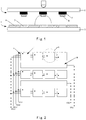
- FIG. 1 is schematic sectional view showing an In-cell touch display panel in the prior art.
- Figure 2 is a top view of touch scanning electrodes and touch sensing electrodes in the touch display panel shown in Figure 1 . As shown in Figs.
- the touch display panel includes: an array substrate 1 and a color filter substrate 2 that are provided opposite to each other, wherein the array substrate 1 includes a first base substrate 3 and a common electrode layer disposed on the first base substrate, where the common electrode layer is divided into a number of blocked touch sensing electrodes 4 and a number of stripped common electrodes 5 extending in a row direction, and wherein the touch sensing electrodes 4 and the stripped common electrodes 5 are alternately disposed in a column direction.
- each of the touch sensing electrodes 4 is connected to a peripheral region of the array substrate by a lateral lead 9 (lateral leads 9 correspond to the touch sensing electrodes one by one and lateral leads 9 are connected to the touch sensing electrodes through vias (not shown)), and all the lateral leads 9 corresponding to all the touch sensing electrodes 4 in the same column are electrically connected to receive touch sensing signals RX (only RX1, RX2, RX3, RX4 are exemplarily shown in Figures).
- the color filter substrate 2 includes a second base substrate 6 and black matrixes 7 disposed on the second base substrate 6, wherein the black matrixes 7 define pixel regions and light-shielding regions. Stripped touch scanning electrodes 8 are disposed in the light-shielding regions. The touch scanning electrodes 8 are disposed opposite to the stripped common electrodes 5.
- a region A shown in Figure 2 that is touched by the finger is taken as an example, that is, a location at which the touch sensing electrode 4 in the first row and in the third column is disposed is touched. At this time, a location at which the touch sensing electrode 4 in the first row and in the second column is disposed will be touched by the edge of the finger touch, so that touch interference occurs at the edge of the finger.
- the lateral lead connecting the touch sensing electrode 4 in the first row and in the third column passes through the touch sensing electrode 4 in the first row and in the second column, when the lateral lead carries touch sensing signal RX3, a certain degree of crosstalk to the touch sensing signal RX2 in the touch sensing electrode 4 in the first row and in the second column will occur.
- the amount of interferences on the touch sensing electrode 4 is large, such that the amount of change of the capacitance corresponding to the touch sensing electrode 4 in the first row and in the second column is large and such that the region corresponding to the touch sensing electrode 4 in the first row and in the second column is incorrectly identified as a touch region.
- the present disclosure provides a touch display panel, a driving method for the same and a touch display device, which can effectively avoid the region near the actual touch region from being incorrectly identified as a touch region, thereby being able to effectively improve the accuracy of the touch display panel.
- the present disclosure provides a touch display panel, including: a plurality of first electrode groups arranged in a first direction and a plurality of second electrode groups arranged in a second direction, wherein each of the first electrode groups includes a plurality of first electrodes arranged in the second direction, and each of the second electrode groups includes a plurality of second electrode subgroups disposed adjacent to each other and arranged in the second direction, each of the second electrode subgroups including a plurality of second electrodes arranged in the first direction; wherein the first electrodes and the second electrodes are disposed in different layers respectively, and projections of the second electrodes on the layer in which the first electrodes are disposed do not overlap with the first electrodes and are alternately arranged with the first electrodes in both the first direction and the second direction; wherein a first lead connected to a peripheral region of the touch display panel is disposed on each of the first electrodes, all the first leads corresponding to the respective first electrodes in a same first electrode group are electrically connected to each other in the peripheral
- a second lead connected to the peripheral region of the touch display panel is disposed on each of the second electrode groups; and the second lead is electrically connected to the second electrode in the corresponding second electrode group closest to the peripheral region of the touch display panel.
- the touch display panel includes an array substrate and an assembling substrate disposed opposite to the array substrate, wherein the first electrodes are disposed on the array substrate and the second electrodes are disposed on the assembling substrate.
- the array substrate includes a first base substrate and a plurality of common electrodes disposed on the first base substrate; the first electrodes and the common electrodes are provided in a same layer, and the first electrodes and the common electrodes are alternately disposed in both the first direction and the second direction.
- the first electrodes and the common electrodes are same in shape.
- the assembling substrate includes a second base substrate and a light-shielding layer disposed on the second base substrate; the material of the second electrodes is a metallic material, and the second electrodes are disposed above the light-shielding layer.
- the material of the second electrodes is a transparent conductive material.
- the present disclosure also provides a touch display device including a touch display panel that is the touch display panel described above.
- the present disclosure also provides a driving method for a touch display panel, wherein the touch display panel is a touch display panel described above, and the second electrodes are connected to the peripheral region through second leads, wherein when the first electrodes are touch scanning electrodes and the second electrodes are touch sensing electrodes, the driving method for the touch display panel including:
- the touch display panel includes an array substrate and an assembling substrate disposed opposite to the array substrate, wherein the first electrodes are disposed on the array substrate and the second electrodes are disposed on the assembling substrate.
- the array substrate includes a first base substrate and a plurality of common electrodes disposed on the first base substrate; the first electrodes and the common electrodes are provided in a same layer; and the first electrodes and the common electrodes are alternately disposed in both the first direction and the second direction.
- the driving method for the touch display panel then includes:
- Figure 3 is a top view of a touch display panel provided in a first embodiment of the present invention
- Figure 4 is a schematic distribution view of first electrodes in Figure 3
- Figure 5 is a schematic distribution view of second electrodes in Figure 3
- the touch display panel includes a plurality of first electrode groups 18 and a plurality of second electrode groups 19, wherein all of the first electrode groups 18 are arranged in a first direction and all of the second electrode groups 19 are arrange in a second direction; wherein each of the first electrode groups 18 includes a plurality of first electrodes 11 arranged in the second direction, and each of the second electrode groups 19 includes a plurality of second electrode subgroups 20 disposed adjacent to each other and arranged in the second direction, each of the second electrode subgroups 20 including a plurality of second electrodes 15 arranged in the first direction.
- the first electrodes 11 and the second electrodes 15 are disposed in different layers, and projections of the second electrodes 15 on the layer in which the first electrodes 11 are disposed do not overlap with the first electrodes 11 and are alternately arranged with the first electrodes 11 in both the first direction and the second direction.
- a first lead 13 connected to a peripheral region of the touch display panel is disposed on each of the first electrodes 11, all the first leads 13 corresponding to all the respective first electrodes 11 in the same first electrode group 18 are electrically connected to each other in the peripheral region; and all the second electrodes 15 in the same second electrode group 19 are electrically connected to each other.
- one of the first electrode 11 and the second electrode 15 serves as a touch scanning electrode, and the other of the first electrode 11 and the second electrode 15 serves as a touch sensing electrode.
- each of the second electrode groups may generate a corresponding touch scanning signal TX (only TX1, TX2 are exemplarily shown in Figures), each of the second electrode groups can generate a corresponding touch sensing signal RX (only RX1, RX2, RX3, RX4 are exemplarily shown in Figures).
- corresponding conductive strips 16 which are disposed in a same layer as the second electrodes 15 is provided such that all the second electrodes 15 in the same second electrode group 19 are electrically connected to each other.
- only one second lead 17 that is connected to the peripheral region of the touch display panel is required to be correspondingly provided for each of the second electrode groups 19, which can effectively reduce the number of peripheral leads of the touch display panel.
- the second lead 17 is electrically connected to the second electrode 15 of the respective second electrode group 19 closest to the peripheral region of the touch display panel. Then, the wiring length of the second lead 17 can be effectively reduced.
- the second electrode subgroups in the second electrode group there are just two second electrode subgroups in the second electrode group, that is, every two adjacent rows of second electrodes may be simultaneously driven.
- the maximization of touch resolution of the touch display panel can be achieved while it is ensured that each region on the touch display panel can achieve touch identification.
- any one of the first electrodes 11 near the actual touch region will not be subject to the two above interferences at the same time.
- a region B in Figure 3 will be taken as an example of the actual touch region that is touched by the finger to be described in the following, that is, the location where the first electrode 11 in the first row and in the third column is located is touched. Then, in particular, the first electrodes 11 near the region B include the first electrode 11 in the first row and in the first column, the first electrode 11 in the second row and in the second column, and the first electrode 11 in the second row and in the fourth column.
- the first electrode 11 in the second row and in the second column and the first electrode 11 in the second row and in the fourth column will be subject to the touch interference caused by the finger edge.
- the first lead corresponding to the first electrode 11 in the first row and in the third column does not pass through the region where the first electrode 11 in the second row and in the second column is located and the region where the first electrode 11 in the second row and in the fourth column is located, the first electrode 11 in the second row and in the second column and the first electrode 11 in the second row and in the fourth column will not be subject to the lead crosstalk interference. Therefore, the amount of interference which the first electrode 11 in the second row and in the second column and the first electrode 11 in the second row and in the fourth column will be subject to is small.
- the first electrode 11 in the first row and in the first column since the first lead corresponding to the first electrode 11 in the first row and in the third column passes through the region where the first electrode 11 in the first row and in the first column is located, the first electrode 11 in the first row and in the first column is located will be subject to the lead crosstalk interference.
- the first electrode 11 in the first row and in the first column since the first electrode 11 in the first row and in the first column is far away from the first electrode 11 in the first row and in the third column (the distance therebetween is larger than the width of one second electrode 12), the first electrode 11 in the first row and in the first column will not be subject to the touch interference caused by the finger edge. Therefore, the amount of interference which the first electrode 11 in the first row and in the first column will be subject to is small.
- the touch display panel includes an array substrate and an assembling substrate disposed opposite to the array substrate, wherein the first electrodes are disposed on the array substrate and the second electrodes are disposed on the assembling substrate.
- Figure 6 is a top view of the array substrate in the first embodiment of the present invention.
- the array substrate further includes a first base substrate 3 and a plurality of common electrodes 12 disposed on the first base substrate 3; the first electrodes 11 and the common electrodes 12 are provided in a same layer; and the first electrodes 11 and the common electrodes 12 are alternately disposed in both the first direction and the second direction.
- the first electrodes 11 and the common electrodes 12 then can be simultaneously prepared in one patterning process.
- first electrodes 11 in the present solution may be used as touch electrodes in the touch phase and may be used as common electrodes in the display phase.
- the specific solution will be described in detail in the following.
- a third lead 14 connected to the peripheral region of the touch display panel is disposed on each of the common electrodes 12, and all of the third leads 14 on the array substrate 14 are electrically connected to each other in the peripheral region of the array substrate in order to obtain an electrical connection to each other among all the common electrodes 12.
- the means in the present embodiment by which all the common electrodes 12 on the array substrate are electrically connected is not intended to be limited to that shown in Figure 3 , and other means can also be employed to obtain the electrical connection among all the common electrodes 12, which will not be illustratively described.
- first electrodes and the common electrodes are the same in shape. Since the first electrodes 11 and the common electrodes 12 are the same in shape, the first electrodes 11 and the common electrodes 12 can be uniformly distributed in the array substrate, which can effectively improve the uniformity of display effect of the touch display panel.
- Figure 7 is a top view of the assembling substrate in the first embodiment of the present invention.
- the assembling substrate includes a second base substrate 6 and a light-shielding layer (not shown) disposed on the second base substrate 6; the material of the second electrode 15 is a metallic material, and the second electrodes 15 are disposed above the light-shielding layer.
- the material of the second electrode 15 is a metallic material (such as Al, Mo, Cr, and so on), it is necessary to ensure that the light-shielding layer (not shown) in the assembling substrate does cover the second electrodes 15 completely.
- the second electrode 15 may be particularly of a metallic grid structure.
- the material of the second electrode 15 may also be a transparent conductive material (for example, ITO), and then it may be unnecessary for the second electrode 15 to be covered by a light shielding layer.
- ITO transparent conductive material
- a second embodiment of the present invention provides a touch display device including a touch display panel that is the touch display panel described in the above first embodiment.
- the specific description can be found in the contents described in the first embodiment, which will not be described in detail here.
- a third embodiment of the present invention provides a driving method for a touch display panel, wherein the touch display panel is the touch display panel described in the above first embodiment, the specific structure of which can be found in the contents described in the first embodiment.
- FIG 8 is a flow chart of a driving method for a touch display panel provided in the third embodiment of the invention. As shown in Figure 8 , when the first electrodes in the touch display panel are touch scanning electrodes and the second electrodes are touch sensing electrodes, the driving method for the touch display panel includes:
- a touch scanning signal is firstly provided to the corresponding first electrode by the first lead and then a touch sensing signal on the second electrode is detected by the second lead.
- the driving method further includes:
- the step 102 in this embodiment may be performed prior to the step 101.
- the touch display panel operates in an operating period of the above-described step 101 and step 102 and repeatedly operates, obtaining a continuous display and touch identification.
- the principle of the touch display panel based on the driving method described above to achieve the pixel display and the touch identification will not be repeated here.
- FIG 9 is a flowchart of another driving method for a touch display panel provided in the third embodiment of the invention. As shown in Figure 9 , when the first electrodes in the touch display panel are touch sensing electrodes and the second electrodes are touch scanning electrodes, the driving method for the touch display panel includes:
- a touch scanning signal is firstly provided to the corresponding second electrode by the second lead and then a touch sensing signal on the first electrode is detected by the first lead.
- the driving method further includes:
- the step 202 in this embodiment may be performed prior to the step 201.
- the touch display panel operates in an operating period of the above-described step 201 and step 202 and repeatedly operates, obtaining a continuous display and touch identification.
Landscapes
- Engineering & Computer Science (AREA)
- General Engineering & Computer Science (AREA)
- Theoretical Computer Science (AREA)
- Human Computer Interaction (AREA)
- Physics & Mathematics (AREA)
- General Physics & Mathematics (AREA)
- Quality & Reliability (AREA)
- Position Input By Displaying (AREA)
Applications Claiming Priority (2)
| Application Number | Priority Date | Filing Date | Title |
|---|---|---|---|
| CN201510223671.9A CN104765506B (zh) | 2015-05-05 | 2015-05-05 | 触控显示面板及其驱动方法和触控显示装置 |
| PCT/CN2015/092671 WO2016176971A1 (fr) | 2015-05-05 | 2015-10-23 | Panneau d'affichage tactile et son procédé de commande, et dispositif d'affichage tactile |
Publications (3)
| Publication Number | Publication Date |
|---|---|
| EP3293614A1 true EP3293614A1 (fr) | 2018-03-14 |
| EP3293614A4 EP3293614A4 (fr) | 2019-01-02 |
| EP3293614B1 EP3293614B1 (fr) | 2022-02-16 |
Family
ID=53647381
Family Applications (1)
| Application Number | Title | Priority Date | Filing Date |
|---|---|---|---|
| EP15866396.3A Not-in-force EP3293614B1 (fr) | 2015-05-05 | 2015-10-23 | Panneau d'affichage tactile et son procédé de commande, et dispositif d'affichage tactile |
Country Status (6)
| Country | Link |
|---|---|
| US (1) | US10216341B2 (fr) |
| EP (1) | EP3293614B1 (fr) |
| JP (1) | JP2018514821A (fr) |
| KR (1) | KR101969028B1 (fr) |
| CN (1) | CN104765506B (fr) |
| WO (1) | WO2016176971A1 (fr) |
Families Citing this family (10)
| Publication number | Priority date | Publication date | Assignee | Title |
|---|---|---|---|---|
| CN104765506B (zh) * | 2015-05-05 | 2019-01-08 | 京东方科技集团股份有限公司 | 触控显示面板及其驱动方法和触控显示装置 |
| KR102387632B1 (ko) * | 2015-09-24 | 2022-04-15 | 엘지디스플레이 주식회사 | 표시패널 및 이를 이용한 표시장치 |
| CN105760012B (zh) * | 2016-01-29 | 2019-12-17 | 厦门天马微电子有限公司 | 触控显示装置及触控显示面板 |
| CN105607783B (zh) * | 2016-03-24 | 2019-06-07 | 上海天马微电子有限公司 | 一种触控显示面板 |
| CN106371665B (zh) * | 2016-08-31 | 2019-07-16 | 厦门天马微电子有限公司 | 一种触控显示面板、驱动方法及触控显示装置 |
| US10067603B1 (en) * | 2017-05-03 | 2018-09-04 | Himax Technologies Limited | Touch panel and sensing method of touch panel capable of simultaneously activating columns of sensors within one drive cycle |
| CN111209889A (zh) * | 2019-05-16 | 2020-05-29 | 神盾股份有限公司 | 指纹传感器 |
| CN119536551A (zh) * | 2020-09-28 | 2025-02-28 | 京东方科技集团股份有限公司 | 触控结构及显示设备 |
| CN114489382B (zh) * | 2022-01-27 | 2024-11-05 | 上海天马微电子有限公司 | 触控面板和触控装置 |
| CN116133458B (zh) * | 2023-02-06 | 2026-01-30 | 昆山国显光电有限公司 | 触控显示面板及显示装置 |
Family Cites Families (22)
| Publication number | Priority date | Publication date | Assignee | Title |
|---|---|---|---|---|
| CN101672660B (zh) * | 2008-04-10 | 2013-01-02 | 爱特梅尔公司 | 电容性位置传感器 |
| TWI395006B (zh) * | 2009-09-09 | 2013-05-01 | Au Optronics Corp | 觸控顯示面板 |
| DE102010020180A1 (de) | 2010-05-11 | 2011-11-17 | Maschinenfabrik Reinhausen Gmbh | Lastumschalter für einen Stufenschalter |
| KR20120100488A (ko) | 2011-03-04 | 2012-09-12 | 하이디스 테크놀로지 주식회사 | 정전용량 터치 패널 및 그 제조방법 |
| CN202182995U (zh) * | 2011-09-09 | 2012-04-04 | 北京京东方光电科技有限公司 | 彩膜基板及电容式触摸屏 |
| TWI439916B (zh) | 2011-10-28 | 2014-06-01 | Sentelic Corp | 電容式觸控板結構及其製造方法 |
| TW201409297A (zh) | 2012-08-21 | 2014-03-01 | Wintek Corp | 觸控感測電極結構及觸控裝置 |
| CN104737109A (zh) * | 2012-10-15 | 2015-06-24 | 松下知识产权经营株式会社 | 输入装置及液晶显示装置 |
| CN103049155A (zh) * | 2012-12-13 | 2013-04-17 | 北京京东方光电科技有限公司 | 一种内嵌式触摸屏及显示装置 |
| CN103049156B (zh) * | 2012-12-13 | 2015-12-23 | 北京京东方光电科技有限公司 | 一种电容式内嵌触摸屏及显示装置 |
| CN103257770B (zh) * | 2013-04-16 | 2016-09-28 | 北京京东方光电科技有限公司 | 一种电容式触摸阵列基板、触摸显示屏及其驱动方法 |
| TWI552038B (zh) | 2013-05-08 | 2016-10-01 | Gunze Kk | Touch panels, display devices and electronic devices |
| US20140375590A1 (en) * | 2013-06-19 | 2014-12-25 | Ronald Steven Cok | Multi-resolution micro-wire touch-sensing method |
| CN103412675B (zh) * | 2013-07-26 | 2016-07-27 | 北京京东方光电科技有限公司 | 一种阵列基板、内嵌式触摸屏及显示装置 |
| CN103838431B (zh) * | 2014-02-24 | 2017-03-01 | 北京京东方光电科技有限公司 | 一种内嵌式触摸屏及显示装置 |
| CN103838430B (zh) * | 2014-02-24 | 2017-01-11 | 北京京东方光电科技有限公司 | 一种内嵌式触摸屏及显示装置 |
| CN103995633B (zh) * | 2014-05-06 | 2017-03-22 | 京东方科技集团股份有限公司 | 一种触控显示装置及其驱动方法 |
| CN104090678A (zh) | 2014-06-27 | 2014-10-08 | 京东方科技集团股份有限公司 | 一种阵列基板、显示装置及其驱动方法 |
| CN104123039B (zh) * | 2014-07-10 | 2017-08-01 | 京东方科技集团股份有限公司 | 一种内嵌式触控显示装置及其驱动方法 |
| CN104391600B (zh) | 2014-11-06 | 2017-11-10 | 京东方科技集团股份有限公司 | 一种内嵌式触摸屏及显示装置 |
| CN104393021B (zh) * | 2014-11-28 | 2018-07-17 | 京东方科技集团股份有限公司 | 像素结构、透明触摸显示屏及其制作方法、和显示装置 |
| CN104765506B (zh) | 2015-05-05 | 2019-01-08 | 京东方科技集团股份有限公司 | 触控显示面板及其驱动方法和触控显示装置 |
-
2015
- 2015-05-05 CN CN201510223671.9A patent/CN104765506B/zh not_active Expired - Fee Related
- 2015-10-23 WO PCT/CN2015/092671 patent/WO2016176971A1/fr not_active Ceased
- 2015-10-23 JP JP2016564310A patent/JP2018514821A/ja active Pending
- 2015-10-23 EP EP15866396.3A patent/EP3293614B1/fr not_active Not-in-force
- 2015-10-23 KR KR1020167029744A patent/KR101969028B1/ko not_active Expired - Fee Related
- 2015-10-23 US US15/104,523 patent/US10216341B2/en active Active
Also Published As
| Publication number | Publication date |
|---|---|
| CN104765506A (zh) | 2015-07-08 |
| EP3293614B1 (fr) | 2022-02-16 |
| US20170115769A1 (en) | 2017-04-27 |
| EP3293614A4 (fr) | 2019-01-02 |
| WO2016176971A1 (fr) | 2016-11-10 |
| US10216341B2 (en) | 2019-02-26 |
| KR101969028B1 (ko) | 2019-04-16 |
| JP2018514821A (ja) | 2018-06-07 |
| CN104765506B (zh) | 2019-01-08 |
| KR20160143698A (ko) | 2016-12-14 |
Similar Documents
| Publication | Publication Date | Title |
|---|---|---|
| EP3293614B1 (fr) | Panneau d'affichage tactile et son procédé de commande, et dispositif d'affichage tactile | |
| CN106502444B (zh) | 触控显示装置及其驱动方法以及压力检测方法 | |
| EP3151096B1 (fr) | Structure tactile capacitive, écran tactile intégré, dispositif d'affichage et procédé de balayage correspondant | |
| TWI669644B (zh) | Touch panel and touch display device | |
| EP2755077B1 (fr) | Substrat de film couleur et écran tactile capacitif | |
| EP2811379B1 (fr) | Dispositif d'affichage tactile à cristaux liquides | |
| EP2990916B1 (fr) | Électrode de capteur tactile, écran tactile et dispositif d'affichage | |
| US9791953B2 (en) | Touch display device and method for driving the touch display device | |
| US10156923B2 (en) | In-cell touch display panel, driving method thereof and display device | |
| CN108398822B (zh) | 触控显示基板、显示面板和显示装置 | |
| EP3153956B1 (fr) | Structure tactile capacitive, écran tactile intégré, dispositif d'affichage, et procédé de balayage correspondant | |
| US20160349889A1 (en) | In Cell Touch Panel And Method For Driving The Same, And Display Device | |
| CN104951143B (zh) | 一种阵列基板、触控面板及显示装置 | |
| US20140362030A1 (en) | Capacitive touch screen and method for manufacturing the same | |
| EP3244292A1 (fr) | Panneau tactile en cellule et dispositif d'affichage | |
| EP3270271B1 (fr) | Écran tactile dans une cellule et dispositif d'affichage | |
| US20210365148A1 (en) | Touch substrate, display device and method for acquiring touch coordinate | |
| KR20150073539A (ko) | 전자장치의 입력 감지장치 및 방법 | |
| CN106648195A (zh) | 触控显示装置及其驱动方法 | |
| CN104460080A (zh) | 触控显示装置 | |
| US10976591B2 (en) | Color filter substrate and method for preparing the same, and touch screen | |
| TWM495570U (zh) | 觸控電極結構及應用其的觸控面板 | |
| CN108920011B (zh) | 显示面板及其驱动方法、显示装置 | |
| KR102281616B1 (ko) | 터치 스크린 패널 및 터치 스크린 패널 제조 방법 | |
| US20160077632A1 (en) | Layer Electrode For Touchscreen |
Legal Events
| Date | Code | Title | Description |
|---|---|---|---|
| STAA | Information on the status of an ep patent application or granted ep patent |
Free format text: STATUS: THE INTERNATIONAL PUBLICATION HAS BEEN MADE |
|
| PUAI | Public reference made under article 153(3) epc to a published international application that has entered the european phase |
Free format text: ORIGINAL CODE: 0009012 |
|
| STAA | Information on the status of an ep patent application or granted ep patent |
Free format text: STATUS: REQUEST FOR EXAMINATION WAS MADE |
|
| 17P | Request for examination filed |
Effective date: 20160616 |
|
| AK | Designated contracting states |
Kind code of ref document: A1 Designated state(s): AL AT BE BG CH CY CZ DE DK EE ES FI FR GB GR HR HU IE IS IT LI LT LU LV MC MK MT NL NO PL PT RO RS SE SI SK SM TR |
|
| AX | Request for extension of the european patent |
Extension state: BA ME |
|
| DAV | Request for validation of the european patent (deleted) | ||
| DAX | Request for extension of the european patent (deleted) | ||
| A4 | Supplementary search report drawn up and despatched |
Effective date: 20181205 |
|
| RIC1 | Information provided on ipc code assigned before grant |
Ipc: G06F 3/044 20060101ALI20181129BHEP Ipc: G06F 3/041 20060101AFI20181129BHEP |
|
| STAA | Information on the status of an ep patent application or granted ep patent |
Free format text: STATUS: EXAMINATION IS IN PROGRESS |
|
| 17Q | First examination report despatched |
Effective date: 20200826 |
|
| GRAP | Despatch of communication of intention to grant a patent |
Free format text: ORIGINAL CODE: EPIDOSNIGR1 |
|
| STAA | Information on the status of an ep patent application or granted ep patent |
Free format text: STATUS: GRANT OF PATENT IS INTENDED |
|
| INTG | Intention to grant announced |
Effective date: 20210914 |
|
| GRAS | Grant fee paid |
Free format text: ORIGINAL CODE: EPIDOSNIGR3 |
|
| GRAA | (expected) grant |
Free format text: ORIGINAL CODE: 0009210 |
|
| STAA | Information on the status of an ep patent application or granted ep patent |
Free format text: STATUS: THE PATENT HAS BEEN GRANTED |
|
| AK | Designated contracting states |
Kind code of ref document: B1 Designated state(s): AL AT BE BG CH CY CZ DE DK EE ES FI FR GB GR HR HU IE IS IT LI LT LU LV MC MK MT NL NO PL PT RO RS SE SI SK SM TR |
|
| REG | Reference to a national code |
Ref country code: GB Ref legal event code: FG4D |
|
| REG | Reference to a national code |
Ref country code: CH Ref legal event code: EP |
|
| REG | Reference to a national code |
Ref country code: DE Ref legal event code: R096 Ref document number: 602015077001 Country of ref document: DE |
|
| REG | Reference to a national code |
Ref country code: AT Ref legal event code: REF Ref document number: 1469303 Country of ref document: AT Kind code of ref document: T Effective date: 20220315 |
|
| REG | Reference to a national code |
Ref country code: IE Ref legal event code: FG4D |
|
| REG | Reference to a national code |
Ref country code: LT Ref legal event code: MG9D |
|
| REG | Reference to a national code |
Ref country code: NL Ref legal event code: MP Effective date: 20220216 |
|
| REG | Reference to a national code |
Ref country code: AT Ref legal event code: MK05 Ref document number: 1469303 Country of ref document: AT Kind code of ref document: T Effective date: 20220216 |
|
| PG25 | Lapsed in a contracting state [announced via postgrant information from national office to epo] |
Ref country code: SE Free format text: LAPSE BECAUSE OF FAILURE TO SUBMIT A TRANSLATION OF THE DESCRIPTION OR TO PAY THE FEE WITHIN THE PRESCRIBED TIME-LIMIT Effective date: 20220216 Ref country code: RS Free format text: LAPSE BECAUSE OF FAILURE TO SUBMIT A TRANSLATION OF THE DESCRIPTION OR TO PAY THE FEE WITHIN THE PRESCRIBED TIME-LIMIT Effective date: 20220216 Ref country code: PT Free format text: LAPSE BECAUSE OF FAILURE TO SUBMIT A TRANSLATION OF THE DESCRIPTION OR TO PAY THE FEE WITHIN THE PRESCRIBED TIME-LIMIT Effective date: 20220616 Ref country code: NO Free format text: LAPSE BECAUSE OF FAILURE TO SUBMIT A TRANSLATION OF THE DESCRIPTION OR TO PAY THE FEE WITHIN THE PRESCRIBED TIME-LIMIT Effective date: 20220516 Ref country code: NL Free format text: LAPSE BECAUSE OF FAILURE TO SUBMIT A TRANSLATION OF THE DESCRIPTION OR TO PAY THE FEE WITHIN THE PRESCRIBED TIME-LIMIT Effective date: 20220216 Ref country code: LT Free format text: LAPSE BECAUSE OF FAILURE TO SUBMIT A TRANSLATION OF THE DESCRIPTION OR TO PAY THE FEE WITHIN THE PRESCRIBED TIME-LIMIT Effective date: 20220216 Ref country code: HR Free format text: LAPSE BECAUSE OF FAILURE TO SUBMIT A TRANSLATION OF THE DESCRIPTION OR TO PAY THE FEE WITHIN THE PRESCRIBED TIME-LIMIT Effective date: 20220216 Ref country code: ES Free format text: LAPSE BECAUSE OF FAILURE TO SUBMIT A TRANSLATION OF THE DESCRIPTION OR TO PAY THE FEE WITHIN THE PRESCRIBED TIME-LIMIT Effective date: 20220216 Ref country code: BG Free format text: LAPSE BECAUSE OF FAILURE TO SUBMIT A TRANSLATION OF THE DESCRIPTION OR TO PAY THE FEE WITHIN THE PRESCRIBED TIME-LIMIT Effective date: 20220516 |
|
| PG25 | Lapsed in a contracting state [announced via postgrant information from national office to epo] |
Ref country code: PL Free format text: LAPSE BECAUSE OF FAILURE TO SUBMIT A TRANSLATION OF THE DESCRIPTION OR TO PAY THE FEE WITHIN THE PRESCRIBED TIME-LIMIT Effective date: 20220216 Ref country code: LV Free format text: LAPSE BECAUSE OF FAILURE TO SUBMIT A TRANSLATION OF THE DESCRIPTION OR TO PAY THE FEE WITHIN THE PRESCRIBED TIME-LIMIT Effective date: 20220216 Ref country code: GR Free format text: LAPSE BECAUSE OF FAILURE TO SUBMIT A TRANSLATION OF THE DESCRIPTION OR TO PAY THE FEE WITHIN THE PRESCRIBED TIME-LIMIT Effective date: 20220517 Ref country code: FI Free format text: LAPSE BECAUSE OF FAILURE TO SUBMIT A TRANSLATION OF THE DESCRIPTION OR TO PAY THE FEE WITHIN THE PRESCRIBED TIME-LIMIT Effective date: 20220216 Ref country code: AT Free format text: LAPSE BECAUSE OF FAILURE TO SUBMIT A TRANSLATION OF THE DESCRIPTION OR TO PAY THE FEE WITHIN THE PRESCRIBED TIME-LIMIT Effective date: 20220216 |
|
| PG25 | Lapsed in a contracting state [announced via postgrant information from national office to epo] |
Ref country code: IS Free format text: LAPSE BECAUSE OF FAILURE TO SUBMIT A TRANSLATION OF THE DESCRIPTION OR TO PAY THE FEE WITHIN THE PRESCRIBED TIME-LIMIT Effective date: 20220617 |
|
| PG25 | Lapsed in a contracting state [announced via postgrant information from national office to epo] |
Ref country code: SM Free format text: LAPSE BECAUSE OF FAILURE TO SUBMIT A TRANSLATION OF THE DESCRIPTION OR TO PAY THE FEE WITHIN THE PRESCRIBED TIME-LIMIT Effective date: 20220216 Ref country code: SK Free format text: LAPSE BECAUSE OF FAILURE TO SUBMIT A TRANSLATION OF THE DESCRIPTION OR TO PAY THE FEE WITHIN THE PRESCRIBED TIME-LIMIT Effective date: 20220216 Ref country code: RO Free format text: LAPSE BECAUSE OF FAILURE TO SUBMIT A TRANSLATION OF THE DESCRIPTION OR TO PAY THE FEE WITHIN THE PRESCRIBED TIME-LIMIT Effective date: 20220216 Ref country code: EE Free format text: LAPSE BECAUSE OF FAILURE TO SUBMIT A TRANSLATION OF THE DESCRIPTION OR TO PAY THE FEE WITHIN THE PRESCRIBED TIME-LIMIT Effective date: 20220216 Ref country code: DK Free format text: LAPSE BECAUSE OF FAILURE TO SUBMIT A TRANSLATION OF THE DESCRIPTION OR TO PAY THE FEE WITHIN THE PRESCRIBED TIME-LIMIT Effective date: 20220216 Ref country code: CZ Free format text: LAPSE BECAUSE OF FAILURE TO SUBMIT A TRANSLATION OF THE DESCRIPTION OR TO PAY THE FEE WITHIN THE PRESCRIBED TIME-LIMIT Effective date: 20220216 |
|
| REG | Reference to a national code |
Ref country code: DE Ref legal event code: R097 Ref document number: 602015077001 Country of ref document: DE |
|
| PG25 | Lapsed in a contracting state [announced via postgrant information from national office to epo] |
Ref country code: AL Free format text: LAPSE BECAUSE OF FAILURE TO SUBMIT A TRANSLATION OF THE DESCRIPTION OR TO PAY THE FEE WITHIN THE PRESCRIBED TIME-LIMIT Effective date: 20220216 |
|
| PLBE | No opposition filed within time limit |
Free format text: ORIGINAL CODE: 0009261 |
|
| STAA | Information on the status of an ep patent application or granted ep patent |
Free format text: STATUS: NO OPPOSITION FILED WITHIN TIME LIMIT |
|
| 26N | No opposition filed |
Effective date: 20221117 |
|
| PG25 | Lapsed in a contracting state [announced via postgrant information from national office to epo] |
Ref country code: SI Free format text: LAPSE BECAUSE OF FAILURE TO SUBMIT A TRANSLATION OF THE DESCRIPTION OR TO PAY THE FEE WITHIN THE PRESCRIBED TIME-LIMIT Effective date: 20220216 |
|
| PG25 | Lapsed in a contracting state [announced via postgrant information from national office to epo] |
Ref country code: MC Free format text: LAPSE BECAUSE OF FAILURE TO SUBMIT A TRANSLATION OF THE DESCRIPTION OR TO PAY THE FEE WITHIN THE PRESCRIBED TIME-LIMIT Effective date: 20220216 |
|
| REG | Reference to a national code |
Ref country code: CH Ref legal event code: PL |
|
| REG | Reference to a national code |
Ref country code: BE Ref legal event code: MM Effective date: 20221031 |
|
| GBPC | Gb: european patent ceased through non-payment of renewal fee |
Effective date: 20221023 |
|
| PG25 | Lapsed in a contracting state [announced via postgrant information from national office to epo] |
Ref country code: LU Free format text: LAPSE BECAUSE OF NON-PAYMENT OF DUE FEES Effective date: 20221023 |
|
| PG25 | Lapsed in a contracting state [announced via postgrant information from national office to epo] |
Ref country code: LI Free format text: LAPSE BECAUSE OF NON-PAYMENT OF DUE FEES Effective date: 20221031 Ref country code: IT Free format text: LAPSE BECAUSE OF FAILURE TO SUBMIT A TRANSLATION OF THE DESCRIPTION OR TO PAY THE FEE WITHIN THE PRESCRIBED TIME-LIMIT Effective date: 20220216 Ref country code: FR Free format text: LAPSE BECAUSE OF NON-PAYMENT OF DUE FEES Effective date: 20221031 Ref country code: CH Free format text: LAPSE BECAUSE OF NON-PAYMENT OF DUE FEES Effective date: 20221031 |
|
| PG25 | Lapsed in a contracting state [announced via postgrant information from national office to epo] |
Ref country code: BE Free format text: LAPSE BECAUSE OF NON-PAYMENT OF DUE FEES Effective date: 20221031 |
|
| PG25 | Lapsed in a contracting state [announced via postgrant information from national office to epo] |
Ref country code: IE Free format text: LAPSE BECAUSE OF NON-PAYMENT OF DUE FEES Effective date: 20221023 Ref country code: GB Free format text: LAPSE BECAUSE OF NON-PAYMENT OF DUE FEES Effective date: 20221023 |
|
| PGFP | Annual fee paid to national office [announced via postgrant information from national office to epo] |
Ref country code: DE Payment date: 20231020 Year of fee payment: 9 |
|
| PG25 | Lapsed in a contracting state [announced via postgrant information from national office to epo] |
Ref country code: HU Free format text: LAPSE BECAUSE OF FAILURE TO SUBMIT A TRANSLATION OF THE DESCRIPTION OR TO PAY THE FEE WITHIN THE PRESCRIBED TIME-LIMIT; INVALID AB INITIO Effective date: 20151023 |
|
| PG25 | Lapsed in a contracting state [announced via postgrant information from national office to epo] |
Ref country code: CY Free format text: LAPSE BECAUSE OF FAILURE TO SUBMIT A TRANSLATION OF THE DESCRIPTION OR TO PAY THE FEE WITHIN THE PRESCRIBED TIME-LIMIT Effective date: 20220216 |
|
| PG25 | Lapsed in a contracting state [announced via postgrant information from national office to epo] |
Ref country code: MK Free format text: LAPSE BECAUSE OF FAILURE TO SUBMIT A TRANSLATION OF THE DESCRIPTION OR TO PAY THE FEE WITHIN THE PRESCRIBED TIME-LIMIT Effective date: 20220216 |
|
| PG25 | Lapsed in a contracting state [announced via postgrant information from national office to epo] |
Ref country code: TR Free format text: LAPSE BECAUSE OF FAILURE TO SUBMIT A TRANSLATION OF THE DESCRIPTION OR TO PAY THE FEE WITHIN THE PRESCRIBED TIME-LIMIT Effective date: 20220216 |
|
| PG25 | Lapsed in a contracting state [announced via postgrant information from national office to epo] |
Ref country code: MT Free format text: LAPSE BECAUSE OF FAILURE TO SUBMIT A TRANSLATION OF THE DESCRIPTION OR TO PAY THE FEE WITHIN THE PRESCRIBED TIME-LIMIT Effective date: 20220216 |
|
| REG | Reference to a national code |
Ref country code: DE Ref legal event code: R119 Ref document number: 602015077001 Country of ref document: DE |
|
| PG25 | Lapsed in a contracting state [announced via postgrant information from national office to epo] |
Ref country code: DE Free format text: LAPSE BECAUSE OF NON-PAYMENT OF DUE FEES Effective date: 20250501 |