EP3294046B1 - Module d'éclairage à semi-conducteur et son procédé de fabrication - Google Patents
Module d'éclairage à semi-conducteur et son procédé de fabrication Download PDFInfo
- Publication number
- EP3294046B1 EP3294046B1 EP16188098.4A EP16188098A EP3294046B1 EP 3294046 B1 EP3294046 B1 EP 3294046B1 EP 16188098 A EP16188098 A EP 16188098A EP 3294046 B1 EP3294046 B1 EP 3294046B1
- Authority
- EP
- European Patent Office
- Prior art keywords
- lighting module
- light emitting
- electrically conductive
- emitting element
- electronic component
- Prior art date
- Legal status (The legal status is an assumption and is not a legal conclusion. Google has not performed a legal analysis and makes no representation as to the accuracy of the status listed.)
- Active
Links
Images



Classifications
-
- H—ELECTRICITY
- H05—ELECTRIC TECHNIQUES NOT OTHERWISE PROVIDED FOR
- H05K—PRINTED CIRCUITS; CASINGS OR CONSTRUCTIONAL DETAILS OF ELECTRIC APPARATUS; MANUFACTURE OF ASSEMBLAGES OF ELECTRICAL COMPONENTS
- H05K1/00—Printed circuits
- H05K1/02—Details
- H05K1/0277—Bendability or stretchability details
- H05K1/0278—Rigid circuit boards or rigid supports of circuit boards locally made bendable, e.g. by removal or replacement of material
-
- H—ELECTRICITY
- H05—ELECTRIC TECHNIQUES NOT OTHERWISE PROVIDED FOR
- H05K—PRINTED CIRCUITS; CASINGS OR CONSTRUCTIONAL DETAILS OF ELECTRIC APPARATUS; MANUFACTURE OF ASSEMBLAGES OF ELECTRICAL COMPONENTS
- H05K1/00—Printed circuits
- H05K1/02—Details
- H05K1/0277—Bendability or stretchability details
- H05K1/028—Bending or folding regions of flexible printed circuits
-
- H—ELECTRICITY
- H05—ELECTRIC TECHNIQUES NOT OTHERWISE PROVIDED FOR
- H05K—PRINTED CIRCUITS; CASINGS OR CONSTRUCTIONAL DETAILS OF ELECTRIC APPARATUS; MANUFACTURE OF ASSEMBLAGES OF ELECTRICAL COMPONENTS
- H05K1/00—Printed circuits
- H05K1/18—Printed circuits structurally associated with non-printed electric components
- H05K1/189—Printed circuits structurally associated with non-printed electric components characterised by the use of flexible or folded printed circuits
-
- H—ELECTRICITY
- H05—ELECTRIC TECHNIQUES NOT OTHERWISE PROVIDED FOR
- H05K—PRINTED CIRCUITS; CASINGS OR CONSTRUCTIONAL DETAILS OF ELECTRIC APPARATUS; MANUFACTURE OF ASSEMBLAGES OF ELECTRICAL COMPONENTS
- H05K2201/00—Indexing scheme relating to printed circuits covered by H05K1/00
- H05K2201/01—Dielectrics
- H05K2201/0137—Materials
- H05K2201/0154—Polyimide
-
- H—ELECTRICITY
- H05—ELECTRIC TECHNIQUES NOT OTHERWISE PROVIDED FOR
- H05K—PRINTED CIRCUITS; CASINGS OR CONSTRUCTIONAL DETAILS OF ELECTRIC APPARATUS; MANUFACTURE OF ASSEMBLAGES OF ELECTRICAL COMPONENTS
- H05K2201/00—Indexing scheme relating to printed circuits covered by H05K1/00
- H05K2201/05—Flexible printed circuits [FPCs]
- H05K2201/055—Folded back on itself
-
- H—ELECTRICITY
- H05—ELECTRIC TECHNIQUES NOT OTHERWISE PROVIDED FOR
- H05K—PRINTED CIRCUITS; CASINGS OR CONSTRUCTIONAL DETAILS OF ELECTRIC APPARATUS; MANUFACTURE OF ASSEMBLAGES OF ELECTRICAL COMPONENTS
- H05K2201/00—Indexing scheme relating to printed circuits covered by H05K1/00
- H05K2201/09—Shape and layout
- H05K2201/09009—Substrate related
- H05K2201/09063—Holes or slots in insulating substrate not used for electrical connections
-
- H—ELECTRICITY
- H05—ELECTRIC TECHNIQUES NOT OTHERWISE PROVIDED FOR
- H05K—PRINTED CIRCUITS; CASINGS OR CONSTRUCTIONAL DETAILS OF ELECTRIC APPARATUS; MANUFACTURE OF ASSEMBLAGES OF ELECTRICAL COMPONENTS
- H05K2201/00—Indexing scheme relating to printed circuits covered by H05K1/00
- H05K2201/09—Shape and layout
- H05K2201/09209—Shape and layout details of conductors
- H05K2201/09218—Conductive traces
- H05K2201/09263—Meander
-
- H—ELECTRICITY
- H05—ELECTRIC TECHNIQUES NOT OTHERWISE PROVIDED FOR
- H05K—PRINTED CIRCUITS; CASINGS OR CONSTRUCTIONAL DETAILS OF ELECTRIC APPARATUS; MANUFACTURE OF ASSEMBLAGES OF ELECTRICAL COMPONENTS
- H05K2201/00—Indexing scheme relating to printed circuits covered by H05K1/00
- H05K2201/10—Details of components or other objects attached to or integrated in a printed circuit board
- H05K2201/10007—Types of components
- H05K2201/10106—Light emitting diode [LED]
Definitions
- the at least one electrically conductive lead is covered at least partly by an electrically insulating protective layer.
- This protective layer firstly provides an electrical insulation of the electrically conductive lead and, secondly, avoids corrosion or abrasion due to environmental influences.
- Such a double layered electrically conductive channel may increase the lifetime of the electrically conductive channel and of the entire electronic device in the following way.
- the second electrically conductive layer may be made of a second material which is less brittle and thus has a smaller risk of breaking under stress than the first electrically conductive layer.
- the second electrically conductive layer forms a bridge over the cracks electrically connecting the disconnected points of the first electrically conductive layer.
- an optimal conductive material can be chosen for the first electrically conductive layer, such as for example copper, even though it may be more brittle and prone to cracking with respect to other conductive materials.
- the second electrically conductive layer made in a less brittle conductive material, can ensure that there is still a conductive connection over the crack.
Landscapes
- Engineering & Computer Science (AREA)
- Microelectronics & Electronic Packaging (AREA)
- Led Device Packages (AREA)
- Fastening Of Light Sources Or Lamp Holders (AREA)
- Structure Of Printed Boards (AREA)
- Electroluminescent Light Sources (AREA)
Claims (11)
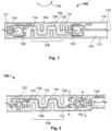
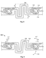
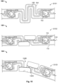
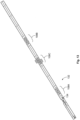
- Module d'éclairage comprenant :un support souple plat, le support souple plat comprenant au moins un substrat souple (104) électriquement isolant, comportant une première surface et une seconde surface, et au moins un conducteur électrique plan (106) qui est disposé sur l'une de la première et de la seconde surface dudit substrat souple (104), etau moins un élément électroluminescent (102) et au moins un composant électronique (124), l'élément électroluminescent (102) et le composant électronique (124, 126) et/ou un second élément électroluminescent (102) étant électriquement reliés l'un à l'autre au moyen dudit conducteur électrique (106),dans lequel, dans au moins une zone étirable, qui fait partie du même support souple plat, ledit conducteur (106) est façonné de sorte à former au moins une boucle de méandre qui s'étend depuis l'axe médian longitudinal (118) au-delà de la première et de la seconde marge (110, 112) du support souple plat à l'extérieur de la zone étirable se déployant le long de l'axe médian longitudinal, et ledit substrat (104) comporte au moins une découpe (114) qui forme une incision qui est ouverte au niveau de la marge (110, 112) du substrat (104) et qui est disposée pour être adjacente à la boucle de méandre de telle sorte que la ou les boucles de méandre encerclent partiellement la découpe (114),dans lequel les parties des boucles qui s'étendent au-delà des marges (110, 112) sont repliées en direction de l'axe médian longitudinal (118) du substrat souple plat (104) de telle sorte qu'il est formé un contour pratiquement droit le long du module d'éclairage (100) le long de la première et de la seconde marge (72, 112).
- Module d'éclairage selon la revendication 1, dans lequel ledit ou lesdits composants électroniques (124, 126) comprennent au moins l'un parmi un condensateur et un connecteur électrique à connecter à un composant électronique externe.
- Module d'éclairage selon l'une des revendications précédentes, dans lequel le ou les éléments électroluminescents (102) comprennent une diode électroluminescente (LED).
- Module d'éclairage selon l'une des revendications précédentes, dans lequel l'élément électroluminescent (102) et/ou le composant électronique (124, 126) comprennent un composant à montage en surface (SMD ou CMS).
- Module d'éclairage selon l'une des revendications précédentes, dans lequel le ou les conducteurs électriques (106) sont couverts au moins partiellement par une couche protectrice (122) électriquement isolante.
- Module d'éclairage selon l'une des revendications précédentes, dans lequel ledit ou lesdits conducteurs électriques (106) comprennent une ligne à ruban séparée d'une couche formant plan de masse par des intervalles s'étirant en parallèle de la ligne à ruban.
- Module d'éclairage selon l'une des revendications précédentes, dans lequel le substrat souple électriquement isolant est fabriqué à partir de polyimide, acrylate ou céramique souple, et/ou dans lequel au moins un conducteur électrique est fabriqué à partir d'un métal ou d'un alliage métallique ou bien à partir d'un polymère comprenant des particules conductrices.
- Module d'éclairage selon l'une des revendications précédentes, comprenant en outre des zones rigides intégrées permettant d'assembler ledit élément électroluminescent et/ou le composant électronique.
- Module d'éclairage selon l'une des revendications précédentes, dans lequel la ou les zones étirables séparent des zones où sont assemblés au moins un élément électroluminescent et/ou un composant électronique.
- Procédé de fabrication d'un module d'éclairage, le procédé comprenant les étapes suivantes :la fabrication d'un support souple plat, le support comprenant au moins un substrat souple (104) électriquement isolant comportant une première surface et une seconde surface et au moins un conducteur électrique plan (106) qui est disposé sur l'une de la première ou de la seconde surface dudit substrat souple, etl'assemblage d'au moins un élément électroluminescent (102) et d'au moins un composant électronique (124), l'élément électroluminescent et le composant électronique/un second élément électroluminescent étant reliés électriquement l'un à l'autre au moyen dudit ou desdits conducteurs électriques,dans lequel, dans au moins une zone étirable, qui fait partie du même support souple plat, ledit conducteur est façonné pour former au moins une boucle de méandre et ledit substrat comporte au moins une découpe (114) qui forme une incision qui est ouverte au niveau de la marge du substrat, et qui est disposée pour être adjacente à la boucle de méandre de telle sorte que la ou les boucles de méandre encerclent partiellement la découpe,dans lequel le support souple plat à l'extérieur de la zone étirable comporte une première et une seconde marge s'étendant le long de l'axe médian longitudinal, et dans lequel, dans la zone étirable, le conducteur électrique forme au moins une boucle de méandre qui se déploie depuis l'axe médian longitudinal au-delà de la première et de la seconde marge, et où le procédé comprend en outre l'étape consistant à replier vers le centre du support souple plat la partie de la boucle qui s'étend au-delà des marges de telle sorte que soit formé un contour pratiquement droit le long de la première et de la seconde marge.
- Procédé selon la revendication 10, dans lequel la découpe est formée par le matriçage du support souple plat.
Priority Applications (2)
| Application Number | Priority Date | Filing Date | Title |
|---|---|---|---|
| EP16188098.4A EP3294046B1 (fr) | 2016-09-09 | 2016-09-09 | Module d'éclairage à semi-conducteur et son procédé de fabrication |
| PCT/EP2017/072179 WO2018046474A1 (fr) | 2016-09-09 | 2017-09-05 | Module d'éclairage à semi-conducteurs et son procédé de fabrication |
Applications Claiming Priority (1)
| Application Number | Priority Date | Filing Date | Title |
|---|---|---|---|
| EP16188098.4A EP3294046B1 (fr) | 2016-09-09 | 2016-09-09 | Module d'éclairage à semi-conducteur et son procédé de fabrication |
Publications (2)
| Publication Number | Publication Date |
|---|---|
| EP3294046A1 EP3294046A1 (fr) | 2018-03-14 |
| EP3294046B1 true EP3294046B1 (fr) | 2023-08-02 |
Family
ID=56896412
Family Applications (1)
| Application Number | Title | Priority Date | Filing Date |
|---|---|---|---|
| EP16188098.4A Active EP3294046B1 (fr) | 2016-09-09 | 2016-09-09 | Module d'éclairage à semi-conducteur et son procédé de fabrication |
Country Status (2)
| Country | Link |
|---|---|
| EP (1) | EP3294046B1 (fr) |
| WO (1) | WO2018046474A1 (fr) |
Families Citing this family (6)
| Publication number | Priority date | Publication date | Assignee | Title |
|---|---|---|---|---|
| TWI797140B (zh) * | 2018-06-25 | 2023-04-01 | 晶元光電股份有限公司 | 具有可伸張軟性載板的發光裝置 |
| RU2689297C1 (ru) * | 2018-09-27 | 2019-05-27 | Федеральное государственное бюджетное учреждение "Национальный исследовательский центр "Курчатовский институт" | Способ синхронизации устройств в накопительных электронных синхротронах источников синхротронного излучения |
| JP7026367B1 (ja) * | 2021-07-20 | 2022-02-28 | エレファンテック株式会社 | 配線基板及びその製造方法 |
| IT202100027629A1 (it) * | 2021-10-28 | 2023-04-28 | Linea Light S R L | Striscia luminosa e relativo metodo di fabbricazione |
| CN114709186B (zh) * | 2022-04-06 | 2024-11-29 | 甬矽电子(宁波)股份有限公司 | 基板和基板制作方法 |
| DE202023105865U1 (de) * | 2023-10-11 | 2025-01-14 | Zumtobel Lighting Gmbh | Leiterplatte mit variablem Abstand ihrer Abschnitte |
Family Cites Families (5)
| Publication number | Priority date | Publication date | Assignee | Title |
|---|---|---|---|---|
| GB2034102A (en) * | 1978-10-02 | 1980-05-29 | Xerox Corp | Flat cable |
| JP4932632B2 (ja) * | 2007-08-06 | 2012-05-16 | 真也 石田 | フレキシブルledモジュールによる表示システム |
| KR200448772Y1 (ko) * | 2009-11-02 | 2010-05-17 | 백성곤 | 휠 수 있는 엘이디 바 |
| US9337404B2 (en) * | 2011-03-22 | 2016-05-10 | Koninklijke Philips N.V. | Substrate for mounting a plurality of light emitting elements |
| DE102012100663A1 (de) * | 2012-01-26 | 2013-08-01 | Sumida Flexible Connections Gmbh | Flexibler elektrischer Verbinder |
-
2016
- 2016-09-09 EP EP16188098.4A patent/EP3294046B1/fr active Active
-
2017
- 2017-09-05 WO PCT/EP2017/072179 patent/WO2018046474A1/fr not_active Ceased
Also Published As
| Publication number | Publication date |
|---|---|
| EP3294046A1 (fr) | 2018-03-14 |
| WO2018046474A1 (fr) | 2018-03-15 |
Similar Documents
| Publication | Publication Date | Title |
|---|---|---|
| EP3294046B1 (fr) | Module d'éclairage à semi-conducteur et son procédé de fabrication | |
| US10943740B2 (en) | Electrical connection contact for a ceramic component, a ceramic component, and a component arrangement | |
| US10222036B2 (en) | Method and system for a three-dimensional (3-D) flexible light emitting diode (LED) bar | |
| KR101802484B1 (ko) | 신호 수집과 파워 연결 조립체, 파워 배터리 모듈 및 차량 | |
| US20180368249A1 (en) | Circuit structure | |
| US20080067526A1 (en) | Flexible circuits having improved reliability and thermal dissipation | |
| EP3427555B1 (fr) | Dispositif d'éclairage et procédé correspondant | |
| JP2019216273A (ja) | フレキシブル基板 | |
| EP2845726A1 (fr) | Feuille d'interconnexion électrique | |
| CN104904325B (zh) | 柔性印刷电路 | |
| CN102203504A (zh) | 用于制造柔性的发光带的方法 | |
| CN102365491A (zh) | 具有至少一个发光带的照明系统 | |
| KR20150001427A (ko) | 광원 회로유닛 및 이를 포함하는 조명장치 | |
| EP4177514B1 (fr) | Bande de lampes à del pouvant être pliée dans de multiples directions et structure de chaînes de lampes associée | |
| EP2215899B1 (fr) | Boîtier de jonction | |
| US20100072509A1 (en) | Lead frame assembly, lead frame and insulating housing combination, and led module having the same | |
| US9203009B2 (en) | Electrode module for LED lamp | |
| US7816691B2 (en) | Light-emitting diode having a flexible substrate | |
| KR101300577B1 (ko) | 자동차용 led 램프 및 그 제조방법 | |
| US10477670B2 (en) | Flexible circuit board assembly for LED lamp | |
| US11527689B2 (en) | Optoelectronic assembly, method and molded part | |
| CN115024024A (zh) | 用于将电气组件布置在印刷电路板上的组件载体 | |
| EP3450833B1 (fr) | Dispositif électronique et module d'éclairage | |
| JP2008270421A (ja) | 熱電モジュール | |
| KR101333987B1 (ko) | 연성회로기판에 실장된 led 패키지와 배선구조 |
Legal Events
| Date | Code | Title | Description |
|---|---|---|---|
| PUAI | Public reference made under article 153(3) epc to a published international application that has entered the european phase |
Free format text: ORIGINAL CODE: 0009012 |
|
| STAA | Information on the status of an ep patent application or granted ep patent |
Free format text: STATUS: THE APPLICATION HAS BEEN PUBLISHED |
|
| AK | Designated contracting states |
Kind code of ref document: A1 Designated state(s): AL AT BE BG CH CY CZ DE DK EE ES FI FR GB GR HR HU IE IS IT LI LT LU LV MC MK MT NL NO PL PT RO RS SE SI SK SM TR |
|
| AX | Request for extension of the european patent |
Extension state: BA ME |
|
| STAA | Information on the status of an ep patent application or granted ep patent |
Free format text: STATUS: REQUEST FOR EXAMINATION WAS MADE |
|
| 17P | Request for examination filed |
Effective date: 20180912 |
|
| RBV | Designated contracting states (corrected) |
Designated state(s): AL AT BE BG CH CY CZ DE DK EE ES FI FR GB GR HR HU IE IS IT LI LT LU LV MC MK MT NL NO PL PT RO RS SE SI SK SM TR |
|
| STAA | Information on the status of an ep patent application or granted ep patent |
Free format text: STATUS: EXAMINATION IS IN PROGRESS |
|
| 17Q | First examination report despatched |
Effective date: 20210622 |
|
| GRAP | Despatch of communication of intention to grant a patent |
Free format text: ORIGINAL CODE: EPIDOSNIGR1 |
|
| STAA | Information on the status of an ep patent application or granted ep patent |
Free format text: STATUS: GRANT OF PATENT IS INTENDED |
|
| INTG | Intention to grant announced |
Effective date: 20230320 |
|
| GRAS | Grant fee paid |
Free format text: ORIGINAL CODE: EPIDOSNIGR3 |
|
| GRAA | (expected) grant |
Free format text: ORIGINAL CODE: 0009210 |
|
| STAA | Information on the status of an ep patent application or granted ep patent |
Free format text: STATUS: THE PATENT HAS BEEN GRANTED |
|
| AK | Designated contracting states |
Kind code of ref document: B1 Designated state(s): AL AT BE BG CH CY CZ DE DK EE ES FI FR GB GR HR HU IE IS IT LI LT LU LV MC MK MT NL NO PL PT RO RS SE SI SK SM TR |
|
| REG | Reference to a national code |
Ref country code: GB Ref legal event code: FG4D |
|
| REG | Reference to a national code |
Ref country code: CH Ref legal event code: EP |
|
| REG | Reference to a national code |
Ref country code: DE Ref legal event code: R096 Ref document number: 602016081535 Country of ref document: DE |
|
| REG | Reference to a national code |
Ref country code: IE Ref legal event code: FG4D |
|
| REG | Reference to a national code |
Ref country code: LT Ref legal event code: MG9D |
|
| REG | Reference to a national code |
Ref country code: NL Ref legal event code: MP Effective date: 20230802 |
|
| REG | Reference to a national code |
Ref country code: AT Ref legal event code: MK05 Ref document number: 1596323 Country of ref document: AT Kind code of ref document: T Effective date: 20230802 |
|
| PG25 | Lapsed in a contracting state [announced via postgrant information from national office to epo] |
Ref country code: GR Free format text: LAPSE BECAUSE OF FAILURE TO SUBMIT A TRANSLATION OF THE DESCRIPTION OR TO PAY THE FEE WITHIN THE PRESCRIBED TIME-LIMIT Effective date: 20231103 |
|
| PG25 | Lapsed in a contracting state [announced via postgrant information from national office to epo] |
Ref country code: IS Free format text: LAPSE BECAUSE OF FAILURE TO SUBMIT A TRANSLATION OF THE DESCRIPTION OR TO PAY THE FEE WITHIN THE PRESCRIBED TIME-LIMIT Effective date: 20231202 |
|
| PG25 | Lapsed in a contracting state [announced via postgrant information from national office to epo] |
Ref country code: SE Free format text: LAPSE BECAUSE OF FAILURE TO SUBMIT A TRANSLATION OF THE DESCRIPTION OR TO PAY THE FEE WITHIN THE PRESCRIBED TIME-LIMIT Effective date: 20230802 Ref country code: RS Free format text: LAPSE BECAUSE OF FAILURE TO SUBMIT A TRANSLATION OF THE DESCRIPTION OR TO PAY THE FEE WITHIN THE PRESCRIBED TIME-LIMIT Effective date: 20230802 Ref country code: PT Free format text: LAPSE BECAUSE OF FAILURE TO SUBMIT A TRANSLATION OF THE DESCRIPTION OR TO PAY THE FEE WITHIN THE PRESCRIBED TIME-LIMIT Effective date: 20231204 Ref country code: NO Free format text: LAPSE BECAUSE OF FAILURE TO SUBMIT A TRANSLATION OF THE DESCRIPTION OR TO PAY THE FEE WITHIN THE PRESCRIBED TIME-LIMIT Effective date: 20231102 Ref country code: NL Free format text: LAPSE BECAUSE OF FAILURE TO SUBMIT A TRANSLATION OF THE DESCRIPTION OR TO PAY THE FEE WITHIN THE PRESCRIBED TIME-LIMIT Effective date: 20230802 Ref country code: LV Free format text: LAPSE BECAUSE OF FAILURE TO SUBMIT A TRANSLATION OF THE DESCRIPTION OR TO PAY THE FEE WITHIN THE PRESCRIBED TIME-LIMIT Effective date: 20230802 Ref country code: LT Free format text: LAPSE BECAUSE OF FAILURE TO SUBMIT A TRANSLATION OF THE DESCRIPTION OR TO PAY THE FEE WITHIN THE PRESCRIBED TIME-LIMIT Effective date: 20230802 Ref country code: IS Free format text: LAPSE BECAUSE OF FAILURE TO SUBMIT A TRANSLATION OF THE DESCRIPTION OR TO PAY THE FEE WITHIN THE PRESCRIBED TIME-LIMIT Effective date: 20231202 Ref country code: HR Free format text: LAPSE BECAUSE OF FAILURE TO SUBMIT A TRANSLATION OF THE DESCRIPTION OR TO PAY THE FEE WITHIN THE PRESCRIBED TIME-LIMIT Effective date: 20230802 Ref country code: GR Free format text: LAPSE BECAUSE OF FAILURE TO SUBMIT A TRANSLATION OF THE DESCRIPTION OR TO PAY THE FEE WITHIN THE PRESCRIBED TIME-LIMIT Effective date: 20231103 Ref country code: FI Free format text: LAPSE BECAUSE OF FAILURE TO SUBMIT A TRANSLATION OF THE DESCRIPTION OR TO PAY THE FEE WITHIN THE PRESCRIBED TIME-LIMIT Effective date: 20230802 Ref country code: AT Free format text: LAPSE BECAUSE OF FAILURE TO SUBMIT A TRANSLATION OF THE DESCRIPTION OR TO PAY THE FEE WITHIN THE PRESCRIBED TIME-LIMIT Effective date: 20230802 |
|
| PG25 | Lapsed in a contracting state [announced via postgrant information from national office to epo] |
Ref country code: PL Free format text: LAPSE BECAUSE OF FAILURE TO SUBMIT A TRANSLATION OF THE DESCRIPTION OR TO PAY THE FEE WITHIN THE PRESCRIBED TIME-LIMIT Effective date: 20230802 |
|
| PG25 | Lapsed in a contracting state [announced via postgrant information from national office to epo] |
Ref country code: ES Free format text: LAPSE BECAUSE OF FAILURE TO SUBMIT A TRANSLATION OF THE DESCRIPTION OR TO PAY THE FEE WITHIN THE PRESCRIBED TIME-LIMIT Effective date: 20230802 |
|
| PG25 | Lapsed in a contracting state [announced via postgrant information from national office to epo] |
Ref country code: SM Free format text: LAPSE BECAUSE OF FAILURE TO SUBMIT A TRANSLATION OF THE DESCRIPTION OR TO PAY THE FEE WITHIN THE PRESCRIBED TIME-LIMIT Effective date: 20230802 Ref country code: RO Free format text: LAPSE BECAUSE OF FAILURE TO SUBMIT A TRANSLATION OF THE DESCRIPTION OR TO PAY THE FEE WITHIN THE PRESCRIBED TIME-LIMIT Effective date: 20230802 Ref country code: ES Free format text: LAPSE BECAUSE OF FAILURE TO SUBMIT A TRANSLATION OF THE DESCRIPTION OR TO PAY THE FEE WITHIN THE PRESCRIBED TIME-LIMIT Effective date: 20230802 Ref country code: EE Free format text: LAPSE BECAUSE OF FAILURE TO SUBMIT A TRANSLATION OF THE DESCRIPTION OR TO PAY THE FEE WITHIN THE PRESCRIBED TIME-LIMIT Effective date: 20230802 Ref country code: DK Free format text: LAPSE BECAUSE OF FAILURE TO SUBMIT A TRANSLATION OF THE DESCRIPTION OR TO PAY THE FEE WITHIN THE PRESCRIBED TIME-LIMIT Effective date: 20230802 Ref country code: CZ Free format text: LAPSE BECAUSE OF FAILURE TO SUBMIT A TRANSLATION OF THE DESCRIPTION OR TO PAY THE FEE WITHIN THE PRESCRIBED TIME-LIMIT Effective date: 20230802 Ref country code: SK Free format text: LAPSE BECAUSE OF FAILURE TO SUBMIT A TRANSLATION OF THE DESCRIPTION OR TO PAY THE FEE WITHIN THE PRESCRIBED TIME-LIMIT Effective date: 20230802 |
|
| REG | Reference to a national code |
Ref country code: CH Ref legal event code: PL |
|
| REG | Reference to a national code |
Ref country code: DE Ref legal event code: R097 Ref document number: 602016081535 Country of ref document: DE |
|
| PG25 | Lapsed in a contracting state [announced via postgrant information from national office to epo] |
Ref country code: LU Free format text: LAPSE BECAUSE OF NON-PAYMENT OF DUE FEES Effective date: 20230909 |
|
| REG | Reference to a national code |
Ref country code: BE Ref legal event code: MM Effective date: 20230930 |
|
| PG25 | Lapsed in a contracting state [announced via postgrant information from national office to epo] |
Ref country code: LU Free format text: LAPSE BECAUSE OF NON-PAYMENT OF DUE FEES Effective date: 20230909 Ref country code: MC Free format text: LAPSE BECAUSE OF FAILURE TO SUBMIT A TRANSLATION OF THE DESCRIPTION OR TO PAY THE FEE WITHIN THE PRESCRIBED TIME-LIMIT Effective date: 20230802 |
|
| PLBE | No opposition filed within time limit |
Free format text: ORIGINAL CODE: 0009261 |
|
| STAA | Information on the status of an ep patent application or granted ep patent |
Free format text: STATUS: NO OPPOSITION FILED WITHIN TIME LIMIT |
|
| REG | Reference to a national code |
Ref country code: IE Ref legal event code: MM4A |
|
| PG25 | Lapsed in a contracting state [announced via postgrant information from national office to epo] |
Ref country code: IE Free format text: LAPSE BECAUSE OF NON-PAYMENT OF DUE FEES Effective date: 20230909 |
|
| 26N | No opposition filed |
Effective date: 20240503 |
|
| PG25 | Lapsed in a contracting state [announced via postgrant information from national office to epo] |
Ref country code: CH Free format text: LAPSE BECAUSE OF NON-PAYMENT OF DUE FEES Effective date: 20230930 |
|
| GBPC | Gb: european patent ceased through non-payment of renewal fee |
Effective date: 20231102 |
|
| PG25 | Lapsed in a contracting state [announced via postgrant information from national office to epo] |
Ref country code: IE Free format text: LAPSE BECAUSE OF NON-PAYMENT OF DUE FEES Effective date: 20230909 Ref country code: CH Free format text: LAPSE BECAUSE OF NON-PAYMENT OF DUE FEES Effective date: 20230930 Ref country code: SI Free format text: LAPSE BECAUSE OF FAILURE TO SUBMIT A TRANSLATION OF THE DESCRIPTION OR TO PAY THE FEE WITHIN THE PRESCRIBED TIME-LIMIT Effective date: 20230802 |
|
| PG25 | Lapsed in a contracting state [announced via postgrant information from national office to epo] |
Ref country code: BE Free format text: LAPSE BECAUSE OF NON-PAYMENT OF DUE FEES Effective date: 20230930 |
|
| PG25 | Lapsed in a contracting state [announced via postgrant information from national office to epo] |
Ref country code: GB Free format text: LAPSE BECAUSE OF NON-PAYMENT OF DUE FEES Effective date: 20231102 |
|
| PG25 | Lapsed in a contracting state [announced via postgrant information from national office to epo] |
Ref country code: GB Free format text: LAPSE BECAUSE OF NON-PAYMENT OF DUE FEES Effective date: 20231102 |
|
| PG25 | Lapsed in a contracting state [announced via postgrant information from national office to epo] |
Ref country code: BG Free format text: LAPSE BECAUSE OF FAILURE TO SUBMIT A TRANSLATION OF THE DESCRIPTION OR TO PAY THE FEE WITHIN THE PRESCRIBED TIME-LIMIT Effective date: 20230802 |
|
| PG25 | Lapsed in a contracting state [announced via postgrant information from national office to epo] |
Ref country code: BG Free format text: LAPSE BECAUSE OF FAILURE TO SUBMIT A TRANSLATION OF THE DESCRIPTION OR TO PAY THE FEE WITHIN THE PRESCRIBED TIME-LIMIT Effective date: 20230802 |
|
| PG25 | Lapsed in a contracting state [announced via postgrant information from national office to epo] |
Ref country code: CY Free format text: LAPSE BECAUSE OF FAILURE TO SUBMIT A TRANSLATION OF THE DESCRIPTION OR TO PAY THE FEE WITHIN THE PRESCRIBED TIME-LIMIT; INVALID AB INITIO Effective date: 20160909 |
|
| PG25 | Lapsed in a contracting state [announced via postgrant information from national office to epo] |
Ref country code: HU Free format text: LAPSE BECAUSE OF FAILURE TO SUBMIT A TRANSLATION OF THE DESCRIPTION OR TO PAY THE FEE WITHIN THE PRESCRIBED TIME-LIMIT; INVALID AB INITIO Effective date: 20160909 |
|
| PGFP | Annual fee paid to national office [announced via postgrant information from national office to epo] |
Ref country code: DE Payment date: 20250702 Year of fee payment: 10 |
|
| PGFP | Annual fee paid to national office [announced via postgrant information from national office to epo] |
Ref country code: IT Payment date: 20250825 Year of fee payment: 10 |
|
| PGFP | Annual fee paid to national office [announced via postgrant information from national office to epo] |
Ref country code: FR Payment date: 20250703 Year of fee payment: 10 |
|
| PG25 | Lapsed in a contracting state [announced via postgrant information from national office to epo] |
Ref country code: TR Free format text: LAPSE BECAUSE OF FAILURE TO SUBMIT A TRANSLATION OF THE DESCRIPTION OR TO PAY THE FEE WITHIN THE PRESCRIBED TIME-LIMIT Effective date: 20230802 |