EP3295190B1 - Agencement de tracés conducteurs et dispositif et procédé de détection d'anomalies d'un circuit à semi-conducteurs - Google Patents
Agencement de tracés conducteurs et dispositif et procédé de détection d'anomalies d'un circuit à semi-conducteurs Download PDFInfo
- Publication number
- EP3295190B1 EP3295190B1 EP16722632.3A EP16722632A EP3295190B1 EP 3295190 B1 EP3295190 B1 EP 3295190B1 EP 16722632 A EP16722632 A EP 16722632A EP 3295190 B1 EP3295190 B1 EP 3295190B1
- Authority
- EP
- European Patent Office
- Prior art keywords
- interconnects
- section
- arrangement
- sections
- semiconductor circuit
- Prior art date
- Legal status (The legal status is an assumption and is not a legal conclusion. Google has not performed a legal analysis and makes no representation as to the accuracy of the status listed.)
- Active
Links
Images


Classifications
-
- G—PHYSICS
- G01—MEASURING; TESTING
- G01R—MEASURING ELECTRIC VARIABLES; MEASURING MAGNETIC VARIABLES
- G01R31/00—Arrangements for testing electric properties; Arrangements for locating electric faults; Arrangements for electrical testing characterised by what is being tested not provided for elsewhere
- G01R31/28—Testing of electronic circuits, e.g. by signal tracer
- G01R31/2851—Testing of integrated circuits [IC]
- G01R31/2855—Environmental, reliability or burn-in testing
- G01R31/2856—Internal circuit aspects, e.g. built-in test features; Test chips; Measuring material aspects, e.g. electro migration [EM]
- G01R31/2858—Measuring of material aspects, e.g. electro-migration [EM], hot carrier injection
-
- G—PHYSICS
- G01—MEASURING; TESTING
- G01R—MEASURING ELECTRIC VARIABLES; MEASURING MAGNETIC VARIABLES
- G01R31/00—Arrangements for testing electric properties; Arrangements for locating electric faults; Arrangements for electrical testing characterised by what is being tested not provided for elsewhere
- G01R31/28—Testing of electronic circuits, e.g. by signal tracer
- G01R31/2851—Testing of integrated circuits [IC]
- G01R31/2884—Testing of integrated circuits [IC] using dedicated test connectors, test elements or test circuits on the IC under test
-
- G—PHYSICS
- G01—MEASURING; TESTING
- G01R—MEASURING ELECTRIC VARIABLES; MEASURING MAGNETIC VARIABLES
- G01R31/00—Arrangements for testing electric properties; Arrangements for locating electric faults; Arrangements for electrical testing characterised by what is being tested not provided for elsewhere
- G01R31/36—Arrangements for testing, measuring or monitoring the electrical condition of accumulators or electric batteries, e.g. capacity or state of charge [SoC]
- G01R31/382—Arrangements for monitoring battery or accumulator variables, e.g. SoC
- G01R31/3835—Arrangements for monitoring battery or accumulator variables, e.g. SoC involving only voltage measurements
Definitions
- Integrated circuits include a plurality of highly integrated circuit elements connected via complex metallization, such as transistors, resistors, or capacitors.
- complex metallization such as transistors, resistors, or capacitors.
- currents flow through the metallization, whereby very high current densities can occur due to the small conductor cross-sections or within joints of the metal layers, typically in the range up to 1 mA / cm 2 . This leads to a failure mechanism, the so-called electromigration. Electrons collide with atoms of the interconnect, whereby a momentum transfer takes place, which leads to a displacement or diffusion of the metal atom in the direction of the electron flow.
- interconnect breaks off, ie the interconnect is interrupted and the electrical functionality of the ASIC is no longer present. Rising temperature also increases the effect of electromigration. The effect is also significantly dependent on the self-heating of the interconnect, the waveform of the load, wherein AC currents produce less degradation, the metal used z.
- Known structures from standard testing are based on long-term measurements on individual interconnects, and record the most critical dimension of the interconnect at the time of testing, in which the strongest electromigration is present, in order to determine the maximum load capacity.
- the aim of the qualification is not a relative measurement, since corresponding measuring devices can specify absolute values for the resistance and absolute values must be specified for the specification of the maximum load capacity.
- the object of the invention is to determine the degradation of the metallization of the semiconductor circuit.
- the advantage here is that a degradation by electromigration during operation of the semiconductor circuit can be detected in a simple manner and can already be detected before the occurrence of a fault in the semiconductor circuit. Furthermore, it is advantageous that a separate reference structure next to the test structure is not necessary, because wide interconnects degrade decisively slower than interconnects with a critical width or width, the so-called "worst-case" width. Thus, the width of the interconnect of the section may serve as a reference, which has only one interconnect. Thus, the storage of an initial value is not absolutely necessary.
- the device for determining the fault of a semiconductor circuit with an arrangement of resistors comprises a number of differential amplifiers, a number of comparators and a control unit.
- the resistors are arranged in the form of interconnects.
- the number of differential amplifiers corresponds to the number of sections.
- Each differential amplifier generates a voltage difference value, each voltage difference value being assigned to one of the comparators as the first input value.
- a reference value serves the comparators as the second input value.
- the control unit detects output values of the comparators and generates an output signal depending on the output values, which represents the type of error.
- the inventive method for determining the defect of a semiconductor circuit by means of an arrangement of interconnects comprises the steps of determining voltage difference values of each section of the array of interconnects, detecting a reference value, generating an output signal in dependence on the voltage difference values and the reference value and determining the error in dependence on the output signal.
- the method can measure the degradation of the interconnect or the metallization during the operation of the semiconductor circuit.
- the hitherto unknown quantities such as operating temperature, user behavior and material properties are thus accurately recorded and need not be estimated.
- FIG. 1 shows an arrangement 100 of interconnects 117 for fault determination of a semiconductor circuit.
- the arrangement 100 has, for example, five sections 112, 113, 114, 115, 116, which are arranged on a horizontal plane of the semiconductor substrate.
- the sections 112, 113, 114, 115, 116 are connected in series. In this case, each section 112, 113, 114, 115, 116 has a specific number of interconnects 117.
- a section 112, 113, 114, 115, 116 comprises at least one interconnect 117. If a section 112, 113, 114, 115, 116 has more than one interconnect 117, the interconnects 117 in this section 112, 113, 114, 115, 116 arranged parallel to each other.
- the arrangement 100 has a first supply line 110 and a second supply line 111.
- the first supply line 110 is electrically connected to the section 116 of the arrangement 100, which comprises the largest number of interconnects 117.
- the second supply line 111 is electrically connected to the section 112 of the arrangement 100, which has a single interconnect 117.
- a first voltage potential can be applied to the first supply line 110 and a second voltage potential can be applied or connected to the second supply line 111.
- the first voltage potential is from the second Voltage potential different.
- the second voltage potential may be grounded.
- the interconnects 117 in a section 112, 113, 114, 115, 116 or within a section 112, 113, 114, 115, 116 each have the same width. In other words, in a section or sector, all metal tracks have the same width, the sum of the widths being approximately identical for each sector. Since the width of the interconnect influences the resistance of the interconnect, it may be necessary to make slight adjustments to the width with the aim of compensating for the edge component of the resistance value. In addition, it ensures identical resistance values per sector. If the arrangement of the interconnects, here also called detector, applied in the application with power, resulting in accordance with the resistors very similar voltage drops, difference ⁇ 5%.
- each section 112, 113, 114, 115, 116 has a metal region 119, which acts as a voltage tap.
- the end section of the previous section is the starting section of the following section.
- the section 116, which has the most parallel interconnects, also has a metal region 119 in the beginning region of the section 116, which acts as a voltage tap.
- the width of the narrowest interconnect 117 is defined by the minimum structure width of the technology and, depending on the technology node and metal level, is in the range of less than 2 ⁇ m.
- the number of interconnects in a section 112, 113, 114, 115, 116 results from the quotient of the widest interconnect 117 and the interconnect width in the respective section 112, 113, 114, 115, 116.
- the width of the "worst-case" Dimension of the interconnects 117 is typically higher than the minimum interconnect dimension, depending on the technology node and metal level in the range between 2 and 8 microns.
- the following values of the interconnects are used in the individual sections: 0.21 ⁇ m, 0.28 ⁇ m, 0.35 ⁇ m, 0.5 ⁇ m, 1.0 ⁇ m, 2.0 ⁇ m, 4.0 ⁇ m, 10.0 ⁇ m.
- the arrangement 100 has intermetallic compounds so-called vias 118.
- the vias 118 act as electrical connections between different, in particular vertically arranged, metal layers of the semiconductor circuit.
- the vias 118 are arranged on the arrangement 100 in the end region of the sections 112, 113, 114, 115, 116, wherein each interconnect 117 has at least one via 118.
- each via 118 essentially has the shape of a cylinder.
- the vias 118 are arranged substantially perpendicular to the interconnects 117 and electrically connected thereto.
- vias 118 are located in the initial region of section 116, which has most interconnects 117.
- the vias 118 allow an electrical connection of the interconnects 117 to another or other level of the semiconductor circuit on which they are more easily accessible, for example, for further processing.
- the vias 118 of a portion 112, 113, 114, 115, 116 are by means of a metal portion 119 on the further level electrically connected. These metal regions 119 act as a voltage tap.
- the further level is below the array 100 within the semiconductor substrate, so that the vias 118 are disposed below the interconnects 117 and the vias 118 electrically contact the interconnects 117 from below.
- the arrangement of the interconnects is not limited to five sections.
- the arrangement of the interconnects can have any number of sections or sectors.
- arrays of interconnects or detectors having a different number of sections are different Metal levels of the semiconductor circuit arranged. In other words, similar detectors are placed one above the other for different metal layers.
- a PN junction is introduced in the underlying semiconductor. Its forward voltage can be used for precise temperature monitoring. Thus, the temperature of the interconnects can be determined. With the additional information of the voltage drop at the interconnects, one can infer a resistance value at the Vormesstemperatur. Thus, the resistance value at the pre-set temperature can be determined and stored as a reference value.
- TCR1 is typically the proportionality constant of the linear component and TCR2 of the quadratic component.
- the device 200 has a number of differential amplifiers 225, 226, 227, which corresponds to the number of sections 212, 213, 214.
- the first supply line 210 is connectable or connected to a first voltage potential
- the second supply line 211 is connected to a second voltage potential.
- the second voltage potential is usually the electrical ground.
- the positive input of each differential amplifier 225, 226, 227 is connected to the output of the series-connected previous section. If it is the differential amplifier 227, which is associated with the section 214 with the most parallel interconnects, so the positive input of the differential amplifier 227 is electrically connected to the first lead 210.
- the negative input of each differential amplifier is connected to the output of section 214.
- the control unit 221 is electrically connected on the input side to the outputs of the comparators 228 and 229, ie the control unit 221 detects the output signals of the comparators 228 and 229
- the control unit 221 generates a signal 224, ie the detector signal indicating the type of error, in response to the output signals of the comparators 228 and 229 by means of the OR gate 230 and the microcontroller 222. That is, the failure mechanism of the semiconductor circuit can be derived from the signal 224, also called detector signal.
- the failure mechanisms of electromigration, stress migration and undercutting of interconnects are also called detector signal.
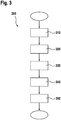
- FIG. 3 shows the method for fault determination of a semiconductor circuit.
- the method starts with step 310, in which each differential voltage amplifier is a first voltage value in an initial region of the respective section as the first Detected input value and detects a second voltage value in the end region of the respective section as a second input value, in order to determine therefrom a voltage difference value and possibly amplify.
- a measuring current is impressed into the arrangement of the interconnects, ie, a current flows in the arrangement of the interconnects. In other words, a current flows through the detector.
- the voltage drop across the individual sectors can be detected with corresponding differential amplifiers.
- a reference value is detected.
- the voltage difference value of a non-degrading section of the resistance arrangement is usually detected as the reference value.
- the section with the widest conductive path is preferably used to determine the reference value.
- the voltage difference value it is also possible to use the voltage difference value as a reference value, which drops over a conductor track which has physical holes in the metal, so that the material transport is inhibited. As a result, a stable reference value can be generated.
- step 330 further voltage difference values are detected.
- the associated voltage difference value which drops across the respective section is detected for each section of the arrangement of the interconnects.
- comparators in particular window comparators
- the individual voltage difference values are compared to the reference voltage value.
- the control unit detects the output values of the individual comparators. The output values are compared by means of an OR gate and an output signal is generated in dependence on the output values, which indicates whether the voltage difference value of one of the sections has exceeded an adjustable tolerance threshold with respect to the voltage difference value of the non-degrading section.
- an error is determined as a function of the output signal. In other words, the error signal can be derived from the detector signal.
- the output signal of the OR gate of the control unit 221 is supplied, which has an analog evaluation circuit or a microcontroller 222 as a digital evaluation circuit.
- control unit has a nonvolatile memory 223 so that voltage difference values can be stored at different times, for example the voltage difference values during an initial measurement.
- the voltage difference in the sections with the minimum width or width of the interconnects will be higher than the reference voltage difference.
- the error mechanism of the undercut of the interconnects typically has a particularly strong influence on the structures with a minimum width, but is already created in the manufacturing process and can already be recognized in an initial measurement depending on the severity.
- the maximum voltage difference between the individual sections is detected as a detector signal, wherein the maximum voltage difference is a measure of the highest change in resistance or resistance deviation of the sections.
- the most degrading sector is determined and output.
- the initial value of the minimum channel width section is an interesting quantity. It correlates strongly with the metal width of the minimal interconnects. This metal width goes into minimal metal resistors, as they are used in analog circuit.
- this track width can be used in the function check to calibrate corresponding analog circuits. Furthermore, the exact determination of the metal resistance for the timing of integrated logic is limiting, as the interconnects become too narrow, the resistance increases, and signal propagation times increase to the point that the logic of the ASIC no longer works. The knowledge of this track width thus gives the opportunity to reduce the maximum allowable clock of the circuit, or to take other measures to nevertheless reach the specified clock, e.g. Increase of the internal supply voltage.
- the evaluation of the detector or the evaluation of the arrangement of the interconnects can be done at different times. Initial at the wafer test, also to check the function of the structure and to store an initial value as a reference value. After the packaging process in the final test step to check the influence of the packaging process. In the field, d. H. Operation of the semiconductor circuit, at each startup procedure or for safety-critical applications also permanently during operation.
- the maximum specification serves as an adjustable tolerance threshold or threshold value. If this is exceeded, a message is sent to the ASIC system or the higher-level controller.
- a general transmission of the detector signal to the ASIC system or the higher-level controller which based on the data of the degradation monitor, possibly in combination with other degradation detectors, recalibrate the ASIC system and can keep at least limited functional.
Landscapes
- Engineering & Computer Science (AREA)
- Physics & Mathematics (AREA)
- General Physics & Mathematics (AREA)
- Computer Hardware Design (AREA)
- Microelectronics & Electronic Packaging (AREA)
- General Engineering & Computer Science (AREA)
- Environmental & Geological Engineering (AREA)
- Semiconductor Integrated Circuits (AREA)
- Testing Or Measuring Of Semiconductors Or The Like (AREA)
Claims (6)
- Agencement (100) de pistes conductrices (117) pour la détermination de défauts d'un circuit à semi-conducteurs, dans lequel les pistes conductrices (117) sont de préférence disposées sur un plan du circuit à semi-conducteurs,• l'agencement (100) présentant plusieurs segments (112, 113, 114, 115, 116), dans lequel les segments (112, 113, 114, 115, 116) sont disposés en tant que montage en série, dans lequel• chaque segment (112, 113, 114, 115, 116) présente un certain nombre de pistes conductrices (117), dans lequel• le nombre de pistes conductrices (117) dans les segments (112, 113, 114, 115, 116) respectifs est différent, dans lequel• chaque segment (112, 113, 114, 115, 116) présente une zone de début et une zone d'extrémité, dans lequel une valeur de différence de tension entre la zone de début et la zone d'extrémité du segment (112, 113, 114, 115, 116) respectif peut être détectée, et les valeurs de différence de tension des segments (112, 113, 114, 115, 116) respectifs sont différentes en cas de défaut,• dans lequel les pistes conductrices (117) de chaque segment (112, 113, 114, 115, 116) sont de même longueur, présentent la même largeur, et sont disposées parallèlement entre elles.
- Agencement (100) de pistes conductrices (117) selon la revendication 1, caractérisé en ce que les largeurs des pistes conductrices (117) sont différentes au moins dans des segments (112, 113, 114, 115, 116) adjacents les uns aux autres.
- Agencement (100) de pistes conductrices (117) selon l'une des revendications précédentes, caractérisé en ce que la piste conductrice (117) la plus étroite de l'agencement (100) présente une largeur qui résulte d'un quotient de la piste conductrice (117) la plus large et du nombre de segments (112, 113, 114, 115, 116).
- Agencement (100) de pistes conductrices (117) selon l'une des revendications précédentes, caractérisé en ce que chaque piste conductrice (117) présente au moins un trou d'interconnexion (118) dans la zone d'extrémité du segment (112, 113, 114, 115, 116) respectif, dans lequel le trou d'interconnexion (118) connecte électriquement la piste conductrice (117) à un autre plan du circuit à semi-conducteurs, de préférence perpendiculairement, de sorte que la valeur de différence de tension de chaque segment (117) dans l'autre plan du circuit à semi-conducteurs peut être détectée, dans lequel les trous d'interconnexion (118) sur l'autre plan sont connectés électriquement à une zone métallique (119) et la zone métallique (119) représente une prise de tension.
- Dispositif (200) pour la détermination de défauts d'un circuit à semi-conducteurs avec un agencement de résistances (215, 216, 217, 218, 219, 220), un certain nombre d'amplificateurs différentiels (225, 226, 227), un certain nombre de comparateurs (228, 229) et une unité de commande (221), caractérisé en ce que les résistances (215, 216, 217, 218, 219, 220) sont disposées sous forme de pistes conductrices (117) selon l'une des revendications précédentes, le nombre d'amplificateurs différentiels (225, 226, 227) correspond au nombre de segments (212, 213, 214), dans lequel chaque amplificateur différentiel (225, 226, 227) génère une valeur de différence de tension, dans lequel respectivement une valeur de différence de tension est respectivement associée à l'un des comparateurs (228, 229) en tant que première valeur d'entrée, dans lequel une valeur de référence est associée aux comparateurs (228, 229) en tant que deuxième valeur d'entrée, et l'unité de commande (221) détecte des valeurs de sortie des comparateurs (228, 229) et génère un signal de sortie (224) en fonction des valeurs de sortie des comparateurs (228, 229), lequel signal représente le type de défaut.
- Procédé (300) pour la détermination de défauts d'un circuit à semi-conducteurs au moyen d'un agencement de pistes conductrices selon l'une des revendications 1 à 4 avec les étapes suivantes :la détermination (310) de valeurs de différence de tension de chaque segment de l'agencement de pistes conductrices,la détection (320) d'une valeur de référence,la génération (330) d'un signal de sortie en fonction des valeurs de différence de tension et de la valeur de référence, etla détermination (340) du défaut en fonction du signal de sortie.
Applications Claiming Priority (2)
| Application Number | Priority Date | Filing Date | Title |
|---|---|---|---|
| DE102015107301 | 2015-05-11 | ||
| PCT/EP2016/060288 WO2016180758A1 (fr) | 2015-05-11 | 2016-05-09 | Agencement de tracés conducteurs et dispositif et procédé de détection d'anomalies d'un circuit à semi-conducteurs |
Publications (2)
| Publication Number | Publication Date |
|---|---|
| EP3295190A1 EP3295190A1 (fr) | 2018-03-21 |
| EP3295190B1 true EP3295190B1 (fr) | 2019-07-10 |
Family
ID=55969132
Family Applications (1)
| Application Number | Title | Priority Date | Filing Date |
|---|---|---|---|
| EP16722632.3A Active EP3295190B1 (fr) | 2015-05-11 | 2016-05-09 | Agencement de tracés conducteurs et dispositif et procédé de détection d'anomalies d'un circuit à semi-conducteurs |
Country Status (4)
| Country | Link |
|---|---|
| US (1) | US10684323B2 (fr) |
| EP (1) | EP3295190B1 (fr) |
| CN (1) | CN107835946B (fr) |
| WO (1) | WO2016180758A1 (fr) |
Families Citing this family (3)
| Publication number | Priority date | Publication date | Assignee | Title |
|---|---|---|---|---|
| WO2017075516A1 (fr) * | 2015-10-29 | 2017-05-04 | The Regents Of The University Of California | Capteur de vieillissement et détection de circuits intégrés de contrefaçon |
| CN112630627B (zh) * | 2021-03-08 | 2021-05-28 | 南京派格测控科技有限公司 | 一种基于多站串测的抽测方法及系统 |
| CN117148204B (zh) * | 2023-09-06 | 2024-03-26 | 惠州市盛微电子有限公司 | 一种大型储能系统电池的安全监控系统及其使用方法 |
Family Cites Families (7)
| Publication number | Priority date | Publication date | Assignee | Title |
|---|---|---|---|---|
| CA2406371A1 (fr) * | 2000-04-17 | 2001-10-25 | Martin Gall | Detection des defaillances precoces d'electromigration dans des interconnexions submicromiques |
| US7851237B2 (en) | 2007-02-23 | 2010-12-14 | Infineon Technologies Ag | Semiconductor device test structures and methods |
| US8253423B2 (en) * | 2007-07-02 | 2012-08-28 | Globalfoundries Inc. | Multiple line width electromigration test structure and method |
| US7521952B2 (en) * | 2007-07-30 | 2009-04-21 | International Business Machines Corporation | Test structure for electromigration analysis and related method |
| JP2011071174A (ja) * | 2009-09-24 | 2011-04-07 | Renesas Electronics Corp | 半導体装置、及び半導体装置の特性劣化検出方法 |
| US8754655B2 (en) | 2011-08-11 | 2014-06-17 | International Business Machines Corporation | Test structure, method and circuit for simultaneously testing time dependent dielectric breakdown and electromigration or stress migration |
| US8890556B2 (en) | 2011-10-26 | 2014-11-18 | International Business Machines Corporation | Real-time on-chip EM performance monitoring |
-
2016
- 2016-05-09 US US15/573,505 patent/US10684323B2/en active Active
- 2016-05-09 EP EP16722632.3A patent/EP3295190B1/fr active Active
- 2016-05-09 WO PCT/EP2016/060288 patent/WO2016180758A1/fr not_active Ceased
- 2016-05-09 CN CN201680040958.0A patent/CN107835946B/zh active Active
Non-Patent Citations (1)
| Title |
|---|
| None * |
Also Published As
| Publication number | Publication date |
|---|---|
| CN107835946B (zh) | 2020-10-23 |
| US10684323B2 (en) | 2020-06-16 |
| CN107835946A (zh) | 2018-03-23 |
| US20180143243A1 (en) | 2018-05-24 |
| WO2016180758A1 (fr) | 2016-11-17 |
| EP3295190A1 (fr) | 2018-03-21 |
Similar Documents
| Publication | Publication Date | Title |
|---|---|---|
| DE10191490B4 (de) | Verfahren und Vorrichtung zur Defektanalyse von integrierten Halbleiterschaltungen | |
| DE102010016184B4 (de) | Prüfung von dielektrischen Filmen und Schichten | |
| EP2542902B1 (fr) | Composant électronique, capteur de courant | |
| DE102006037633B4 (de) | Halbleiterchip mit Beschädigungs-Detektierschaltung und ein Verfahren zum Herstellen eines Halbleiterchips | |
| EP3566034B1 (fr) | Dispositif et procédé d'étalonnage in situ d'un thermomètre | |
| WO2014161624A1 (fr) | Résistance de mesure et procédé de mesure correspondant | |
| EP3411724B1 (fr) | Détecteur de vieillissement d'un composant de circuit électrique, procédé de surveillance du vieillissement d'un composant de circuit, composant et dispositif de commande | |
| DE102008000218A1 (de) | Halbleiteranordnungsteststrukturen und Verfahren | |
| EP3295190B1 (fr) | Agencement de tracés conducteurs et dispositif et procédé de détection d'anomalies d'un circuit à semi-conducteurs | |
| DE102011076651B4 (de) | Stromregelung mit thermisch gepaarten Widerständen | |
| DE112019002516T5 (de) | Nebenschlusswiderstands-Halterungsstruktur | |
| DE102017111410A1 (de) | Messungen in Schaltvorrichtungen | |
| DE102019218308A1 (de) | Widerstandsbaugruppe für Stromsensor sowie Stromsensor und Verfahren zur Messung eines Batteriestroms | |
| DE2408540C2 (de) | Halbleiterbauelement aus einer Vielzahl mindestens annähernd gleicher Schaltungselemente und Verfahren zum Erkennen und Abtrennen defekter Schaltungselemente | |
| WO2002067318A2 (fr) | Structure d'essai d'electromigration pour la determination de la fiabilite de cablages | |
| DE102008022201B4 (de) | Vorrichtung und Verfahren zum Messen einer lokalen Oberflächentemperatur eines Halbleiterbauelements | |
| DE102008057607B4 (de) | Thermoelektrische Leistungsmesszelle und entsprechendes Messverfahren | |
| DE102015210602B4 (de) | Messvorrichtung | |
| EP3637116B1 (fr) | Détecteur et procédé de vérification d'un détecteur | |
| EP1860447B1 (fr) | Dispositif d'essais d'un circuit et procédé d'essais destinés à vérifier un chemin dans un circuit | |
| AT500263B1 (de) | Verfahren und schaltung zum schutz von prüfkontakten bei der hochstrom-messung von halbleiter-bauelementen | |
| DE102020110001B4 (de) | Vorrichtung mit zwei Spannungsdomänen und Verfahren | |
| WO2009080686A1 (fr) | Circuit de contrôle pour un accumulateur d'énergie, et procédé de contrôle d'un accumulateur d'énergie | |
| WO2021048232A1 (fr) | Capteur de batterie | |
| DE10211569A1 (de) | Elektromigration-Teststruktur, Substrat, Elektromigration-Testanordnung und Verfahren zum Ermitteln von Elektromigration |
Legal Events
| Date | Code | Title | Description |
|---|---|---|---|
| STAA | Information on the status of an ep patent application or granted ep patent |
Free format text: STATUS: THE INTERNATIONAL PUBLICATION HAS BEEN MADE |
|
| PUAI | Public reference made under article 153(3) epc to a published international application that has entered the european phase |
Free format text: ORIGINAL CODE: 0009012 |
|
| STAA | Information on the status of an ep patent application or granted ep patent |
Free format text: STATUS: REQUEST FOR EXAMINATION WAS MADE |
|
| 17P | Request for examination filed |
Effective date: 20171211 |
|
| AK | Designated contracting states |
Kind code of ref document: A1 Designated state(s): AL AT BE BG CH CY CZ DE DK EE ES FI FR GB GR HR HU IE IS IT LI LT LU LV MC MK MT NL NO PL PT RO RS SE SI SK SM TR |
|
| AX | Request for extension of the european patent |
Extension state: BA ME |
|
| DAV | Request for validation of the european patent (deleted) | ||
| DAX | Request for extension of the european patent (deleted) | ||
| GRAP | Despatch of communication of intention to grant a patent |
Free format text: ORIGINAL CODE: EPIDOSNIGR1 |
|
| STAA | Information on the status of an ep patent application or granted ep patent |
Free format text: STATUS: GRANT OF PATENT IS INTENDED |
|
| RIC1 | Information provided on ipc code assigned before grant |
Ipc: G01R 31/28 20060101AFI20181130BHEP |
|
| INTG | Intention to grant announced |
Effective date: 20190109 |
|
| GRAS | Grant fee paid |
Free format text: ORIGINAL CODE: EPIDOSNIGR3 |
|
| GRAA | (expected) grant |
Free format text: ORIGINAL CODE: 0009210 |
|
| STAA | Information on the status of an ep patent application or granted ep patent |
Free format text: STATUS: THE PATENT HAS BEEN GRANTED |
|
| AK | Designated contracting states |
Kind code of ref document: B1 Designated state(s): AL AT BE BG CH CY CZ DE DK EE ES FI FR GB GR HR HU IE IS IT LI LT LU LV MC MK MT NL NO PL PT RO RS SE SI SK SM TR |
|
| REG | Reference to a national code |
Ref country code: GB Ref legal event code: FG4D Free format text: NOT ENGLISH |
|
| REG | Reference to a national code |
Ref country code: CH Ref legal event code: EP Ref country code: AT Ref legal event code: REF Ref document number: 1154144 Country of ref document: AT Kind code of ref document: T Effective date: 20190715 |
|
| REG | Reference to a national code |
Ref country code: DE Ref legal event code: R096 Ref document number: 502016005480 Country of ref document: DE |
|
| REG | Reference to a national code |
Ref country code: IE Ref legal event code: FG4D Free format text: LANGUAGE OF EP DOCUMENT: GERMAN |
|
| REG | Reference to a national code |
Ref country code: NL Ref legal event code: MP Effective date: 20190710 |
|
| REG | Reference to a national code |
Ref country code: LT Ref legal event code: MG4D |
|
| PG25 | Lapsed in a contracting state [announced via postgrant information from national office to epo] |
Ref country code: LT Free format text: LAPSE BECAUSE OF FAILURE TO SUBMIT A TRANSLATION OF THE DESCRIPTION OR TO PAY THE FEE WITHIN THE PRESCRIBED TIME-LIMIT Effective date: 20190710 Ref country code: NL Free format text: LAPSE BECAUSE OF FAILURE TO SUBMIT A TRANSLATION OF THE DESCRIPTION OR TO PAY THE FEE WITHIN THE PRESCRIBED TIME-LIMIT Effective date: 20190710 Ref country code: PT Free format text: LAPSE BECAUSE OF FAILURE TO SUBMIT A TRANSLATION OF THE DESCRIPTION OR TO PAY THE FEE WITHIN THE PRESCRIBED TIME-LIMIT Effective date: 20191111 Ref country code: BG Free format text: LAPSE BECAUSE OF FAILURE TO SUBMIT A TRANSLATION OF THE DESCRIPTION OR TO PAY THE FEE WITHIN THE PRESCRIBED TIME-LIMIT Effective date: 20191010 Ref country code: SE Free format text: LAPSE BECAUSE OF FAILURE TO SUBMIT A TRANSLATION OF THE DESCRIPTION OR TO PAY THE FEE WITHIN THE PRESCRIBED TIME-LIMIT Effective date: 20190710 Ref country code: HR Free format text: LAPSE BECAUSE OF FAILURE TO SUBMIT A TRANSLATION OF THE DESCRIPTION OR TO PAY THE FEE WITHIN THE PRESCRIBED TIME-LIMIT Effective date: 20190710 Ref country code: NO Free format text: LAPSE BECAUSE OF FAILURE TO SUBMIT A TRANSLATION OF THE DESCRIPTION OR TO PAY THE FEE WITHIN THE PRESCRIBED TIME-LIMIT Effective date: 20191010 Ref country code: FI Free format text: LAPSE BECAUSE OF FAILURE TO SUBMIT A TRANSLATION OF THE DESCRIPTION OR TO PAY THE FEE WITHIN THE PRESCRIBED TIME-LIMIT Effective date: 20190710 |
|
| PG25 | Lapsed in a contracting state [announced via postgrant information from national office to epo] |
Ref country code: RS Free format text: LAPSE BECAUSE OF FAILURE TO SUBMIT A TRANSLATION OF THE DESCRIPTION OR TO PAY THE FEE WITHIN THE PRESCRIBED TIME-LIMIT Effective date: 20190710 Ref country code: ES Free format text: LAPSE BECAUSE OF FAILURE TO SUBMIT A TRANSLATION OF THE DESCRIPTION OR TO PAY THE FEE WITHIN THE PRESCRIBED TIME-LIMIT Effective date: 20190710 Ref country code: IS Free format text: LAPSE BECAUSE OF FAILURE TO SUBMIT A TRANSLATION OF THE DESCRIPTION OR TO PAY THE FEE WITHIN THE PRESCRIBED TIME-LIMIT Effective date: 20191110 Ref country code: GR Free format text: LAPSE BECAUSE OF FAILURE TO SUBMIT A TRANSLATION OF THE DESCRIPTION OR TO PAY THE FEE WITHIN THE PRESCRIBED TIME-LIMIT Effective date: 20191011 Ref country code: AL Free format text: LAPSE BECAUSE OF FAILURE TO SUBMIT A TRANSLATION OF THE DESCRIPTION OR TO PAY THE FEE WITHIN THE PRESCRIBED TIME-LIMIT Effective date: 20190710 Ref country code: LV Free format text: LAPSE BECAUSE OF FAILURE TO SUBMIT A TRANSLATION OF THE DESCRIPTION OR TO PAY THE FEE WITHIN THE PRESCRIBED TIME-LIMIT Effective date: 20190710 |
|
| PG25 | Lapsed in a contracting state [announced via postgrant information from national office to epo] |
Ref country code: TR Free format text: LAPSE BECAUSE OF FAILURE TO SUBMIT A TRANSLATION OF THE DESCRIPTION OR TO PAY THE FEE WITHIN THE PRESCRIBED TIME-LIMIT Effective date: 20190710 |
|
| RAP2 | Party data changed (patent owner data changed or rights of a patent transferred) |
Owner name: ROBERT BOSCH GMBH |
|
| PG25 | Lapsed in a contracting state [announced via postgrant information from national office to epo] |
Ref country code: RO Free format text: LAPSE BECAUSE OF FAILURE TO SUBMIT A TRANSLATION OF THE DESCRIPTION OR TO PAY THE FEE WITHIN THE PRESCRIBED TIME-LIMIT Effective date: 20190710 Ref country code: DK Free format text: LAPSE BECAUSE OF FAILURE TO SUBMIT A TRANSLATION OF THE DESCRIPTION OR TO PAY THE FEE WITHIN THE PRESCRIBED TIME-LIMIT Effective date: 20190710 Ref country code: EE Free format text: LAPSE BECAUSE OF FAILURE TO SUBMIT A TRANSLATION OF THE DESCRIPTION OR TO PAY THE FEE WITHIN THE PRESCRIBED TIME-LIMIT Effective date: 20190710 Ref country code: PL Free format text: LAPSE BECAUSE OF FAILURE TO SUBMIT A TRANSLATION OF THE DESCRIPTION OR TO PAY THE FEE WITHIN THE PRESCRIBED TIME-LIMIT Effective date: 20190710 |
|
| PG25 | Lapsed in a contracting state [announced via postgrant information from national office to epo] |
Ref country code: CZ Free format text: LAPSE BECAUSE OF FAILURE TO SUBMIT A TRANSLATION OF THE DESCRIPTION OR TO PAY THE FEE WITHIN THE PRESCRIBED TIME-LIMIT Effective date: 20190710 Ref country code: SK Free format text: LAPSE BECAUSE OF FAILURE TO SUBMIT A TRANSLATION OF THE DESCRIPTION OR TO PAY THE FEE WITHIN THE PRESCRIBED TIME-LIMIT Effective date: 20190710 Ref country code: IS Free format text: LAPSE BECAUSE OF FAILURE TO SUBMIT A TRANSLATION OF THE DESCRIPTION OR TO PAY THE FEE WITHIN THE PRESCRIBED TIME-LIMIT Effective date: 20200224 Ref country code: SM Free format text: LAPSE BECAUSE OF FAILURE TO SUBMIT A TRANSLATION OF THE DESCRIPTION OR TO PAY THE FEE WITHIN THE PRESCRIBED TIME-LIMIT Effective date: 20190710 |
|
| REG | Reference to a national code |
Ref country code: DE Ref legal event code: R097 Ref document number: 502016005480 Country of ref document: DE |
|
| PLBE | No opposition filed within time limit |
Free format text: ORIGINAL CODE: 0009261 |
|
| STAA | Information on the status of an ep patent application or granted ep patent |
Free format text: STATUS: NO OPPOSITION FILED WITHIN TIME LIMIT |
|
| PG2D | Information on lapse in contracting state deleted |
Ref country code: IS |
|
| 26N | No opposition filed |
Effective date: 20200603 |
|
| PG25 | Lapsed in a contracting state [announced via postgrant information from national office to epo] |
Ref country code: SI Free format text: LAPSE BECAUSE OF FAILURE TO SUBMIT A TRANSLATION OF THE DESCRIPTION OR TO PAY THE FEE WITHIN THE PRESCRIBED TIME-LIMIT Effective date: 20190710 |
|
| PG25 | Lapsed in a contracting state [announced via postgrant information from national office to epo] |
Ref country code: CH Free format text: LAPSE BECAUSE OF NON-PAYMENT OF DUE FEES Effective date: 20200531 Ref country code: MC Free format text: LAPSE BECAUSE OF FAILURE TO SUBMIT A TRANSLATION OF THE DESCRIPTION OR TO PAY THE FEE WITHIN THE PRESCRIBED TIME-LIMIT Effective date: 20190710 Ref country code: LI Free format text: LAPSE BECAUSE OF NON-PAYMENT OF DUE FEES Effective date: 20200531 |
|
| REG | Reference to a national code |
Ref country code: BE Ref legal event code: MM Effective date: 20200531 |
|
| PG25 | Lapsed in a contracting state [announced via postgrant information from national office to epo] |
Ref country code: LU Free format text: LAPSE BECAUSE OF NON-PAYMENT OF DUE FEES Effective date: 20200509 |
|
| PG25 | Lapsed in a contracting state [announced via postgrant information from national office to epo] |
Ref country code: IE Free format text: LAPSE BECAUSE OF NON-PAYMENT OF DUE FEES Effective date: 20200509 |
|
| PG25 | Lapsed in a contracting state [announced via postgrant information from national office to epo] |
Ref country code: BE Free format text: LAPSE BECAUSE OF NON-PAYMENT OF DUE FEES Effective date: 20200531 |
|
| PG25 | Lapsed in a contracting state [announced via postgrant information from national office to epo] |
Ref country code: MT Free format text: LAPSE BECAUSE OF FAILURE TO SUBMIT A TRANSLATION OF THE DESCRIPTION OR TO PAY THE FEE WITHIN THE PRESCRIBED TIME-LIMIT Effective date: 20190710 Ref country code: CY Free format text: LAPSE BECAUSE OF FAILURE TO SUBMIT A TRANSLATION OF THE DESCRIPTION OR TO PAY THE FEE WITHIN THE PRESCRIBED TIME-LIMIT Effective date: 20190710 |
|
| PG25 | Lapsed in a contracting state [announced via postgrant information from national office to epo] |
Ref country code: MK Free format text: LAPSE BECAUSE OF FAILURE TO SUBMIT A TRANSLATION OF THE DESCRIPTION OR TO PAY THE FEE WITHIN THE PRESCRIBED TIME-LIMIT Effective date: 20190710 |
|
| REG | Reference to a national code |
Ref country code: AT Ref legal event code: MM01 Ref document number: 1154144 Country of ref document: AT Kind code of ref document: T Effective date: 20210509 |
|
| PG25 | Lapsed in a contracting state [announced via postgrant information from national office to epo] |
Ref country code: AT Free format text: LAPSE BECAUSE OF NON-PAYMENT OF DUE FEES Effective date: 20210509 |
|
| PGFP | Annual fee paid to national office [announced via postgrant information from national office to epo] |
Ref country code: GB Payment date: 20250522 Year of fee payment: 10 |
|
| PGFP | Annual fee paid to national office [announced via postgrant information from national office to epo] |
Ref country code: IT Payment date: 20250530 Year of fee payment: 10 |
|
| PGFP | Annual fee paid to national office [announced via postgrant information from national office to epo] |
Ref country code: FR Payment date: 20250521 Year of fee payment: 10 |
|
| PGFP | Annual fee paid to national office [announced via postgrant information from national office to epo] |
Ref country code: DE Payment date: 20250716 Year of fee payment: 10 |