EP3295214B1 - Ionizing radiation detector module - Google Patents
Ionizing radiation detector module Download PDFInfo
- Publication number
- EP3295214B1 EP3295214B1 EP16726004.1A EP16726004A EP3295214B1 EP 3295214 B1 EP3295214 B1 EP 3295214B1 EP 16726004 A EP16726004 A EP 16726004A EP 3295214 B1 EP3295214 B1 EP 3295214B1
- Authority
- EP
- European Patent Office
- Prior art keywords
- detector
- detection
- printed circuit
- circuit board
- carrier
- Prior art date
- Legal status (The legal status is an assumption and is not a legal conclusion. Google has not performed a legal analysis and makes no representation as to the accuracy of the status listed.)
- Active
Links
Images



Classifications
-
- G—PHYSICS
- G01—MEASURING; TESTING
- G01T—MEASUREMENT OF NUCLEAR OR X-RADIATION
- G01T1/00—Measuring X-radiation, gamma radiation, corpuscular radiation, or cosmic radiation
- G01T1/16—Measuring radiation intensity
- G01T1/24—Measuring radiation intensity with semiconductor detectors
- G01T1/243—Modular detectors, e.g. arrays formed from self contained units
-
- G—PHYSICS
- G01—MEASURING; TESTING
- G01T—MEASUREMENT OF NUCLEAR OR X-RADIATION
- G01T1/00—Measuring X-radiation, gamma radiation, corpuscular radiation, or cosmic radiation
- G01T1/16—Measuring radiation intensity
- G01T1/24—Measuring radiation intensity with semiconductor detectors
- G01T1/244—Auxiliary details, e.g. casings, cooling, damping or insulation against damage by, e.g. heat, pressure or the like
-
- G—PHYSICS
- G01—MEASURING; TESTING
- G01T—MEASUREMENT OF NUCLEAR OR X-RADIATION
- G01T1/00—Measuring X-radiation, gamma radiation, corpuscular radiation, or cosmic radiation
- G01T1/16—Measuring radiation intensity
- G01T1/24—Measuring radiation intensity with semiconductor detectors
- G01T1/247—Detector read-out circuitry
Definitions
- the invention relates to the electronic imaging of ionizing radiation detectors with a continuous detection surface.
- hybrid pixel detectors are currently used which utilize, for example, chips known to the professional public under the names Medipix and Timepix. These chips have a sensor layer which is sensitive to ionizing radiation applied to the read-out chip, from the side of which there are connected electrical conductors for supplying power and transmitting communication signals.
- detection chips utilized have a standard-size detector surface which, excluding the non-sensitive periphery, reaches a maximum of several tens of square centimeters. Detection chips with a larger detector surface are not manufactured, because with larger detector surfaces there is a much higher occurrence of errors, making such manufacture unprofitable.
- the detector surface of the detector have a area of up to hundreds of square centimeters while being capable of producing data so that the displayed image is continuous, without dividing edges between the individual detection chips - segments.
- the image from the array of the detection segments are corrected using software, while in other designs detection segments are used which have no edges (edgeless). These edgeless detection segments are arranged next to each other and their operation is synchronized to produce a clear resulting image of the detected ionizing radiation.
- the disadvantages of the design according to this application consist in the fact that due to the lack of space for storing conductors, the detection segments can not have their own communication channel and therefore are connected serially. This limitation in connecting has a negative impact on the data collection rate from the detection segments. Moreover, it is impossible to control the thermal stability of the power source and the detection segments. When connecting detection segments to an independent power source, a temperature difference occurs between the two parts which is difficult to compensate and has a negative effect on the stability of the power supply and the operation of the detection segments. Another disadvantage is that within the continuous surface, there form areas with limited sensitivity of detection, located above the vertical lead of electrical conductors beneath the matrix.
- document WO 2015/027968 discloses a module showing overlapping detector segments and having buses placed on an unoccupied area of the upper surface of a carrier for connecting the output conductors and technical passages between adjacent carriers for placing electronic parts.
- Document EP 1 920 465 B1 shows a regulator on the inside of an L-shaped support structure, whilst document EP 0 291 351 A1 discloses overlapping detector modules with a cooling pipe underneath an overlapping area.
- the objective of the invention is to create a module for the construction of ionizing radiation detectors with a continuous detector surface.
- the modules should allow for the completion of the detector in the form of a row, while the total number of detection segments in a row should not be limited. Alternatively, this would allow for the assembly of a detector with an unlimited rectangular or square detection surface.
- the modules would allow for both serial connection of the detection segments to the readout electronics but also for a high-speed parallel connection, or a combination thereof.
- Another significant feature of the invention should be the integration of power supplies into the structure of the detection module and their position in close proximity to the actual detection segments. This would remove the influence of temperature differences and would secure a stable power supply for the detection segments.
- the ionizing radiation detector module has at least two detection segments arranged side by side on a row carrier with clearance up to 30 ⁇ m to form a continuous detection surface.
- the row carrier is formed by a longitudinal profile having a cross-sectional shape of a square or rectangle, and on at least part of the upper base of the row carrier there are exchangeably arranged holders of the detection segments.
- the detection segment includes an elementary pixel detector consisting of a sensor layer sensitive to detecting radiation and which is arranged on the upper surface of the read-out chip.
- the read-out chip is asymmetrically attached to the holder by at least part of its lower surface while the rest of the lower surface of the chip exceeds the upper base of the row carrier.
- the elemental pixel detector is equipped with at least one output conductor led out horizontally from the side of the read-out chip to the upper base of the carrier for connecting to the power supply and transmitting communication signals to the electronics readout.
- the summary of the invention consists in the fact that on the unoccupied surface of the upper base of the row carrier there is arranged at least one printed circuit board for connecting the output conductors, furthermore there is arranged, towards the row carrier in the area below the level of the upper base of the row carrier to the vertical wall of the row carrier, at least one means for stabilizing the power supply of the elementary pixel detector.
- the means for stabilizing the power supply is connected to the printed circuit board and is further connected with the connector of the electronics readout.
- the connector of the electronics readout is oriented below the row carrier.
- the means for power supply stabilization does not obstruct in a parallel arrangement of the individual modules together into larger continuous detection surfaces of the detectors, and at the same time the existing thermal bridge cancels the temperature difference between the means for power supply stabilization and the row carrier, including the holder of the detection segment. Equalizing the temperature differences using thermal bridges leads to a stabilization of the power supply and thus to a stabilization of the quality of the operation of the elements of the pixel detector.
- the rigid circuit board fulfills the role of electrical conductors, wherein it is dimensionally stable. This arrangement of the components of the module allows for the parallel or serial connection of the detection segments to the data bus of the electronics readout.
- Connecting a rigid circuit board with the means of power supply stabilization and with the connector of the data readout electronics for each individual segment of the detector allows for the data to be read in parallel from all segments simultaneously, thereby achieving a high speed of data acquisition from the detector composed of the modules.
- the invention may be preferably adjusted so that the row carrier is formed in the shape of an "L" profile between the arms of which the segment holder is arranged.
- the holder extends over the upper base of the carrier, while the height of the printed circuit board is the same as the height of the overlap above the upper base.
- the holder is higher than the height difference between the arms of the "L" profile and extends above the upper base of the carrier.
- the height difference between the upper base of the carrier and the holder in the unoccupied surface of the base of the carrier is filled with a rigid printed circuit board.
- the printed circuit board and the row carrier make up an integral element, and the output conductors are more easily connectable to the printed circuit board. This arrangement makes it easier to place the modules together into a continuous detection surface.
- the conductors of the read-out chip are mounted on a holder and are connected to the printed circuit board with wire connections. If the conductors are fixed to the segment holder, they do not tend to break while handling the detection segment, e.g. when assembling the module or when replacing a faulty segment. Soldering a wire connection is fast and cheap compared to forming an assembly consisting of male and female parts.
- the printed circuit board is detachably fixed to the upper base, whereby from the point of fixation the printed circuit has, on at least part of its length, at least one flexible part led vertically downward to the means of power stabilization.
- the flexible part led vertically downward below the row carrier is also preferably used between the means of power stabilization and the connector of the readout electronics.
- the printed circuit board due to its flexible part, may bend from its point of fixation over the edge of the row carrier and lead it along the wall of the row carrier vertically downward to the means of power supply stabilization.
- Using the flexible part of the printed circuit board for connecting to the connector of the readout electronics is preferable when organizing more modules to the detector with a large detector surface, where there is no excess space between the modules.
- the invention also includes an ionizing radiation detector according to claim 7.
- the summary of the invention consists in that the detection surface of the detector comprises at least one continuous row of at least two modules arranged side by side on the matrix.
- the detector in the form of a long continuous row has high detection speed, size independence, and a stability of power supply even when a large number of detection segments are used. Defective or operationally damaged components are easily exchangeable in the detector due to the modular construction.
- the continuous rows of the modules are arranged in parallel next to each other into a continuous detection surface. Due to the parallel arrangement of continuous rows, it is possible to assemble a continuous surface in the shape of, for example, a square.
- the connectors of the data read-out electronics from the detection segments are connected to the readout electronics serially for the serial data reading from individual segments sequentially and/or parallel for the parallel reading of data from all detection segments simultaneously. Connecting the detection segments to read-out electronics is possible serially for applications with lower demands on imaging speed as well as in parallel for applications requiring the detector to work the fastest.
- the row carriers are fastened to the thermally conductive matrix, which may be provided with a heat exchange circuit.
- the thermally conductive matrix regulates the temperature differences and the heat exchange circuit removes excess heat out of the detector.
- the holders of the detection segments, the row carriers, and the thermally conductive matrix are made of aluminum or its alloys.
- Aluminum is a lightweight, stable, and easily accessible material with good thermal conductivity.
- the module for the construction of an ionizing radiation detector allows for the assembly of detectors with an unlimitedly large detection surface.
- the modules can be arranged next to each other both in series and in parallel, the new arrangement of electrical conductors consisting of printed circuit boards resolves the problem of the lack of space between the modules.
- the detection segments in individual modules exhibit reliable operation due to the stable power supply, which is ensured by eliminating the temperature difference between the power supply and the detection segment.
- the arrangement of connections allows for the detection segments to be connected to the read-out electronics in the assembled detectors serially or in parallel. For detectors with a large surface, excess heat is dissipated away from the detector, so the operation of the detector need not be limited in any way.
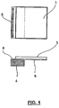
- Fig. 1 shows a detection segment 2 , used in the construction of modules 1 and detectors 14 , which is on a part of its lower surface fastened to a holder 4 of the segment 2 . Thanks to this partial fastening, the overlap 7 of the detection segment 2 is well visible.
- the detection segment 2 is formed by a sensor layer 5 of material that reacts to the effects of ionizing radiation.
- the sensor layer 5 is attached to a read-out chip 6 , which is a semiconductor component.
- the read-out chip 6 is able to register the response of the sensor layer 5 on the incident ionizing radiation on the individual pixels, into which the surface of the segment 2 can be divided. Information about the incident ionizing radiation is transferred by electrical conductors 8 .
- Electrical conductors 8 are led out from the side of the read-out chip 6 and there are at least two of them; one for supplying power, the second for transferring information in the form of voltage changes.
- the detection segment 2 is formed by e.g. a chip known under the name Timepix.
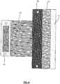
- Fig. 2 shows a module 1 comprising five detection segments 2 edgelessly arranged in a row.
- the segments 2 are orientated with the electrical conductors 8 on one side towards the printed circuit board 9 , which is fixed to the row carrier 3 (not shown) and forms a continuous overlap 7 on the opposite side.
- the electrical conductors 8 are connected with the printed circuit board 9 by conductor wires 12 which can be secured by solder.
- the printed circuit board 9 in the vertically downward direction, has a bent flexible part 13 , which leads to the means 10 for power supply stabilization.
- the printed circuit board 9 is formed by a combination of conductors printed onto a plastic backing which then passes into a series of electrical conductors hidden in waterproof sleeves to ensure the flexibility of the flexible part 13 .
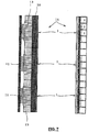
- Fig 3 shows a cross-sectional view of the module 1 from fig. 2 , specifically one of the segments 2 .
- the sensor layer 5 is displayed on the read-out chip 6 , which, with overlap 7 , is attached to the holder 4 of the segment 2 held in the row carrier 3 having an "L" profile.
- the holder 4 is screwed to the carrier 3 and forms a height overlap compared to the upper base 16 of the carrier 3 .
- the holder and the carrier are made of aluminum.
- a printed circuit board 9 which compensates for the height difference.
- the electrical conductors 8 are directed towards the printed circuit board 9 and are connected by a wired connection 12 .
- a means 10 for power supply stabilization On the side of the row carrier 3 is a means 10 for power supply stabilization which is connected to the segment 2 by the flexible part 13 of the printed circuit board 9 , which is bent vertically downwards.
- the flexible part 13 continues from the means 10 of power supply stabilization to the connector 11 of the read-out electronics.
- the connector 11 of the read-out electronics is located, in terms of spatial arrangement, below the row carrier 3 .
- Fig. 4 shows the printed circuit board 9 with unfolded flexible parts 13 .
- the printed circuit board 9 is detachably fixed to the base of the row carrier 3 .
- the flexible part 13 leads to the means 10 of power supply stabilization then continues to the connector 11 of the read-out electronics.
- Fig 5 shows a layout of modules 1 in parallel to each other in which three modules 1 are arranged together, each with five segments 2 .
- Fig. 6 shows a cross-section of the module 1 from fig. 5 . It can be seen how the overlaps 7 are utilized for covering the non-sensitive area of the upper base 16 of the row carrier 3 of each of the modules 1 . Also shown is how the flexible parts 13 of the printed circuit boards 9 are led vertically downwards to avoid interfering and to allow for an independent stable power supply and connecting to the connector 11 for each of the segments 2 .
- Fig. 7 shows the detector 14 as a continuous row.
- the detector 14 is composed of three modules 1 fixed to the matrix 15 .
- Fig. 8 shows an assembly of modules 1 into a continuous detection surface of the detector 14 .
- the modules 1 are lined up next to each other without being limited along the sides.
- the connectors 11 for the read-out electronics, means 10 for power supply stabilization, and flexible part 13 of the printed circuit board 9 are below the detection surface and below the row carriers 3 , so they do not interfere with the assembly of modules 1 to each other.
- the carriage of the modules 1 is secured by a matrix 15 which is made of thermally conductive material and is equipped with a heat exchange circuit.
- the heat transfer medium used in the circuit is water.
- the read-out electronics can be arranged in serial mode for reading individual segments, which is slower, or to parallel reading mode when the detector speed is very high. It is also possible to set a region of interest within a large detector surface from which the detected radiation should be read.
- the ionizing radiation detector module with continuous detection surface, and detectors assembled from modules according to the invention shall find application in industry for testing the quality of products and materials, in the medical field, and in scientific applications.
Landscapes
- Physics & Mathematics (AREA)
- Health & Medical Sciences (AREA)
- Life Sciences & Earth Sciences (AREA)
- General Physics & Mathematics (AREA)
- High Energy & Nuclear Physics (AREA)
- Molecular Biology (AREA)
- Spectroscopy & Molecular Physics (AREA)
- Measurement Of Radiation (AREA)
- Solid State Image Pick-Up Elements (AREA)
Applications Claiming Priority (2)
| Application Number | Priority Date | Filing Date | Title |
|---|---|---|---|
| CZ2015-318A CZ306067B6 (cs) | 2015-05-12 | 2015-05-12 | Modul detektoru ionizujícího záření |
| PCT/CZ2016/000054 WO2016180382A1 (en) | 2015-05-12 | 2016-05-10 | Ionizing radiation detector module |
Publications (2)
| Publication Number | Publication Date |
|---|---|
| EP3295214A1 EP3295214A1 (en) | 2018-03-21 |
| EP3295214B1 true EP3295214B1 (en) | 2020-09-30 |
Family
ID=56092691
Family Applications (1)
| Application Number | Title | Priority Date | Filing Date |
|---|---|---|---|
| EP16726004.1A Active EP3295214B1 (en) | 2015-05-12 | 2016-05-10 | Ionizing radiation detector module |
Country Status (5)
| Country | Link |
|---|---|
| US (1) | US10261199B2 (cs) |
| EP (1) | EP3295214B1 (cs) |
| JP (1) | JP6526239B2 (cs) |
| CZ (1) | CZ306067B6 (cs) |
| WO (1) | WO2016180382A1 (cs) |
Families Citing this family (3)
| Publication number | Priority date | Publication date | Assignee | Title |
|---|---|---|---|---|
| WO2019144324A1 (en) | 2018-01-24 | 2019-08-01 | Shenzhen Xpectvision Technology Co., Ltd. | Packaging of radiation detectors in an image sensor |
| CN109959963B (zh) * | 2019-04-29 | 2024-01-26 | 中国计量科学研究院 | 一种电离室夹具 |
| US12471877B2 (en) * | 2022-06-07 | 2025-11-18 | GE Precision Healthcare LLC | Photon counting computed tomography (PCCT) detector sensor repair for increased sensor yield |
Citations (1)
| Publication number | Priority date | Publication date | Assignee | Title |
|---|---|---|---|---|
| EP0291351A1 (en) * | 1987-05-15 | 1988-11-17 | Shimadzu Corporation | Radiation image detecting apparatus |
Family Cites Families (16)
| Publication number | Priority date | Publication date | Assignee | Title |
|---|---|---|---|---|
| US4338521A (en) * | 1980-05-09 | 1982-07-06 | General Electric Company | Modular radiation detector array and module |
| US5991357A (en) * | 1997-12-16 | 1999-11-23 | Analogic Corporation | Integrated radiation detecting and collimating assembly for X-ray tomography system |
| GB2332608B (en) * | 1997-12-18 | 2000-09-06 | Simage Oy | Modular imaging apparatus |
| JP3818271B2 (ja) * | 2003-04-25 | 2006-09-06 | 株式会社島津製作所 | 放射線撮影装置 |
| WO2006119786A1 (en) | 2005-05-09 | 2006-11-16 | European Organisation For Nuclear Research - Cern | Method for stabilization of dc-potential at the output of a preamplifier and amplifier circuit |
| EP1760787A1 (en) * | 2005-09-02 | 2007-03-07 | Paul Scherrer Institut | An imaging device for single X-ray photon counting |
| JP2007155563A (ja) * | 2005-12-07 | 2007-06-21 | Acrorad Co Ltd | 放射線画像検出装置 |
| JP2009139346A (ja) * | 2007-12-11 | 2009-06-25 | Fuji Electric Systems Co Ltd | 放射線検出センサおよび放射線検出センサユニット |
| WO2010058309A2 (en) * | 2008-11-18 | 2010-05-27 | Koninklijke Philips Electronics N.V. | Spectral imaging detector |
| US8553834B2 (en) * | 2010-09-17 | 2013-10-08 | Analog Devices, Inc. | Computed tomography detector module |
| KR101761817B1 (ko) * | 2011-03-04 | 2017-07-26 | 삼성전자주식회사 | 대면적 엑스선 검출기 |
| US9168008B2 (en) * | 2011-11-03 | 2015-10-27 | General Electric Company | Coarse segmented detector architecture and method of making same |
| IN2014CN03499A (cs) * | 2011-11-08 | 2015-10-09 | Koninkl Philips Nv | |
| JP5619717B2 (ja) * | 2011-12-16 | 2014-11-05 | 株式会社日立製作所 | 放射線検出器用電源回路およびそれを用いた半導体放射線検出装置 |
| US9116022B2 (en) * | 2012-12-07 | 2015-08-25 | Analog Devices, Inc. | Compact sensor module |
| CZ2013669A3 (cs) | 2013-08-30 | 2015-01-07 | České vysoké učení technické v Praze Ústav technické a experimentální fyziky | Detektor ionizujícího záření umožňující vytvoření souvislého digitálního obrazu |
-
2015
- 2015-05-12 CZ CZ2015-318A patent/CZ306067B6/cs unknown
-
2016
- 2016-05-10 WO PCT/CZ2016/000054 patent/WO2016180382A1/en not_active Ceased
- 2016-05-10 US US15/572,818 patent/US10261199B2/en active Active
- 2016-05-10 JP JP2017555710A patent/JP6526239B2/ja active Active
- 2016-05-10 EP EP16726004.1A patent/EP3295214B1/en active Active
Patent Citations (1)
| Publication number | Priority date | Publication date | Assignee | Title |
|---|---|---|---|---|
| EP0291351A1 (en) * | 1987-05-15 | 1988-11-17 | Shimadzu Corporation | Radiation image detecting apparatus |
Also Published As
| Publication number | Publication date |
|---|---|
| JP6526239B2 (ja) | 2019-06-05 |
| CZ2015318A3 (cs) | 2016-07-20 |
| EP3295214A1 (en) | 2018-03-21 |
| JP2018522204A (ja) | 2018-08-09 |
| CZ306067B6 (cs) | 2016-07-20 |
| WO2016180382A1 (en) | 2016-11-17 |
| US20180113224A1 (en) | 2018-04-26 |
| US10261199B2 (en) | 2019-04-16 |
Similar Documents
| Publication | Publication Date | Title |
|---|---|---|
| EP3295214B1 (en) | Ionizing radiation detector module | |
| EP3206051A1 (en) | Radiation imaging device with irregular rectangular shape and extraoral dental imaging system therefrom | |
| EP2417630B1 (en) | A method for manufacturing a radiation imaging panel comprising imaging tiles | |
| US9820389B2 (en) | Partially depopulated interconnection arrays for packaged semiconductor devices and printed circuit boards | |
| US20120069956A1 (en) | Computed tomography detector module | |
| RU2013147397A (ru) | Спектральный детектор изображения | |
| JP2015507742A (ja) | Pet検出器用可撓性コネクタ | |
| US20160209521A1 (en) | Detector of ionizing radiation enabling a coherent digital image | |
| JP5027832B2 (ja) | 放射線検出モジュール及び放射線撮像装置 | |
| CZ28374U1 (cs) | Modul detektoru ionizujícího záření | |
| JP6195134B2 (ja) | 電磁波検知器アセンブリを備える装置およびそのような装置のアセンブリの配置 | |
| CN109478556A (zh) | 检测器模块、检测器、成像设备和制造检测器模块的方法 | |
| US20130182180A1 (en) | High Density Composite Focal Plane Array | |
| JP2007155563A (ja) | 放射線画像検出装置 | |
| US20090109636A1 (en) | Multiple package module using a rigid flex printed circuit board | |
| JP6325920B2 (ja) | 高精細撮像素子用パッケージ | |
| US20250364422A1 (en) | Electronic module and electronic apparatus | |
| US12282123B2 (en) | Readout and processing arrangement in a sensor system | |
| JP2025077598A (ja) | アレイセンサ | |
| EP3355081A1 (en) | Direct conversion compound semiconductor tile structure | |
| JP2015161594A (ja) | 放射線検出器 | |
| JP2011209210A (ja) | 放射線検出器 |
Legal Events
| Date | Code | Title | Description |
|---|---|---|---|
| STAA | Information on the status of an ep patent application or granted ep patent |
Free format text: STATUS: THE INTERNATIONAL PUBLICATION HAS BEEN MADE |
|
| PUAI | Public reference made under article 153(3) epc to a published international application that has entered the european phase |
Free format text: ORIGINAL CODE: 0009012 |
|
| STAA | Information on the status of an ep patent application or granted ep patent |
Free format text: STATUS: REQUEST FOR EXAMINATION WAS MADE |
|
| 17P | Request for examination filed |
Effective date: 20171110 |
|
| AK | Designated contracting states |
Kind code of ref document: A1 Designated state(s): AL AT BE BG CH CY CZ DE DK EE ES FI FR GB GR HR HU IE IS IT LI LT LU LV MC MK MT NL NO PL PT RO RS SE SI SK SM TR |
|
| AX | Request for extension of the european patent |
Extension state: BA ME |
|
| DAV | Request for validation of the european patent (deleted) | ||
| DAX | Request for extension of the european patent (deleted) | ||
| GRAP | Despatch of communication of intention to grant a patent |
Free format text: ORIGINAL CODE: EPIDOSNIGR1 |
|
| STAA | Information on the status of an ep patent application or granted ep patent |
Free format text: STATUS: GRANT OF PATENT IS INTENDED |
|
| INTG | Intention to grant announced |
Effective date: 20200707 |
|
| GRAS | Grant fee paid |
Free format text: ORIGINAL CODE: EPIDOSNIGR3 |
|
| GRAA | (expected) grant |
Free format text: ORIGINAL CODE: 0009210 |
|
| STAA | Information on the status of an ep patent application or granted ep patent |
Free format text: STATUS: THE PATENT HAS BEEN GRANTED |
|
| AK | Designated contracting states |
Kind code of ref document: B1 Designated state(s): AL AT BE BG CH CY CZ DE DK EE ES FI FR GB GR HR HU IE IS IT LI LT LU LV MC MK MT NL NO PL PT RO RS SE SI SK SM TR |
|
| REG | Reference to a national code |
Ref country code: CH Ref legal event code: EP Ref country code: GB Ref legal event code: FG4D |
|
| REG | Reference to a national code |
Ref country code: AT Ref legal event code: REF Ref document number: 1319375 Country of ref document: AT Kind code of ref document: T Effective date: 20201015 |
|
| REG | Reference to a national code |
Ref country code: DE Ref legal event code: R096 Ref document number: 602016044933 Country of ref document: DE |
|
| REG | Reference to a national code |
Ref country code: IE Ref legal event code: FG4D |
|
| REG | Reference to a national code |
Ref country code: CH Ref legal event code: NV Representative=s name: KATZAROV SA, CH |
|
| REG | Reference to a national code |
Ref country code: NL Ref legal event code: FP |
|
| PG25 | Lapsed in a contracting state [announced via postgrant information from national office to epo] |
Ref country code: FI Free format text: LAPSE BECAUSE OF FAILURE TO SUBMIT A TRANSLATION OF THE DESCRIPTION OR TO PAY THE FEE WITHIN THE PRESCRIBED TIME-LIMIT Effective date: 20200930 Ref country code: BG Free format text: LAPSE BECAUSE OF FAILURE TO SUBMIT A TRANSLATION OF THE DESCRIPTION OR TO PAY THE FEE WITHIN THE PRESCRIBED TIME-LIMIT Effective date: 20201230 Ref country code: GR Free format text: LAPSE BECAUSE OF FAILURE TO SUBMIT A TRANSLATION OF THE DESCRIPTION OR TO PAY THE FEE WITHIN THE PRESCRIBED TIME-LIMIT Effective date: 20201231 Ref country code: NO Free format text: LAPSE BECAUSE OF FAILURE TO SUBMIT A TRANSLATION OF THE DESCRIPTION OR TO PAY THE FEE WITHIN THE PRESCRIBED TIME-LIMIT Effective date: 20201230 Ref country code: HR Free format text: LAPSE BECAUSE OF FAILURE TO SUBMIT A TRANSLATION OF THE DESCRIPTION OR TO PAY THE FEE WITHIN THE PRESCRIBED TIME-LIMIT Effective date: 20200930 Ref country code: SE Free format text: LAPSE BECAUSE OF FAILURE TO SUBMIT A TRANSLATION OF THE DESCRIPTION OR TO PAY THE FEE WITHIN THE PRESCRIBED TIME-LIMIT Effective date: 20200930 |
|
| REG | Reference to a national code |
Ref country code: AT Ref legal event code: MK05 Ref document number: 1319375 Country of ref document: AT Kind code of ref document: T Effective date: 20200930 |
|
| PG25 | Lapsed in a contracting state [announced via postgrant information from national office to epo] |
Ref country code: RS Free format text: LAPSE BECAUSE OF FAILURE TO SUBMIT A TRANSLATION OF THE DESCRIPTION OR TO PAY THE FEE WITHIN THE PRESCRIBED TIME-LIMIT Effective date: 20200930 Ref country code: LV Free format text: LAPSE BECAUSE OF FAILURE TO SUBMIT A TRANSLATION OF THE DESCRIPTION OR TO PAY THE FEE WITHIN THE PRESCRIBED TIME-LIMIT Effective date: 20200930 |
|
| REG | Reference to a national code |
Ref country code: LT Ref legal event code: MG4D |
|
| PG25 | Lapsed in a contracting state [announced via postgrant information from national office to epo] |
Ref country code: LT Free format text: LAPSE BECAUSE OF FAILURE TO SUBMIT A TRANSLATION OF THE DESCRIPTION OR TO PAY THE FEE WITHIN THE PRESCRIBED TIME-LIMIT Effective date: 20200930 Ref country code: CZ Free format text: LAPSE BECAUSE OF FAILURE TO SUBMIT A TRANSLATION OF THE DESCRIPTION OR TO PAY THE FEE WITHIN THE PRESCRIBED TIME-LIMIT Effective date: 20200930 Ref country code: RO Free format text: LAPSE BECAUSE OF FAILURE TO SUBMIT A TRANSLATION OF THE DESCRIPTION OR TO PAY THE FEE WITHIN THE PRESCRIBED TIME-LIMIT Effective date: 20200930 Ref country code: SM Free format text: LAPSE BECAUSE OF FAILURE TO SUBMIT A TRANSLATION OF THE DESCRIPTION OR TO PAY THE FEE WITHIN THE PRESCRIBED TIME-LIMIT Effective date: 20200930 Ref country code: PT Free format text: LAPSE BECAUSE OF FAILURE TO SUBMIT A TRANSLATION OF THE DESCRIPTION OR TO PAY THE FEE WITHIN THE PRESCRIBED TIME-LIMIT Effective date: 20210201 Ref country code: EE Free format text: LAPSE BECAUSE OF FAILURE TO SUBMIT A TRANSLATION OF THE DESCRIPTION OR TO PAY THE FEE WITHIN THE PRESCRIBED TIME-LIMIT Effective date: 20200930 |
|
| PG25 | Lapsed in a contracting state [announced via postgrant information from national office to epo] |
Ref country code: ES Free format text: LAPSE BECAUSE OF FAILURE TO SUBMIT A TRANSLATION OF THE DESCRIPTION OR TO PAY THE FEE WITHIN THE PRESCRIBED TIME-LIMIT Effective date: 20200930 Ref country code: AT Free format text: LAPSE BECAUSE OF FAILURE TO SUBMIT A TRANSLATION OF THE DESCRIPTION OR TO PAY THE FEE WITHIN THE PRESCRIBED TIME-LIMIT Effective date: 20200930 Ref country code: AL Free format text: LAPSE BECAUSE OF FAILURE TO SUBMIT A TRANSLATION OF THE DESCRIPTION OR TO PAY THE FEE WITHIN THE PRESCRIBED TIME-LIMIT Effective date: 20200930 Ref country code: PL Free format text: LAPSE BECAUSE OF FAILURE TO SUBMIT A TRANSLATION OF THE DESCRIPTION OR TO PAY THE FEE WITHIN THE PRESCRIBED TIME-LIMIT Effective date: 20200930 Ref country code: IS Free format text: LAPSE BECAUSE OF FAILURE TO SUBMIT A TRANSLATION OF THE DESCRIPTION OR TO PAY THE FEE WITHIN THE PRESCRIBED TIME-LIMIT Effective date: 20210130 |
|
| PG25 | Lapsed in a contracting state [announced via postgrant information from national office to epo] |
Ref country code: SK Free format text: LAPSE BECAUSE OF FAILURE TO SUBMIT A TRANSLATION OF THE DESCRIPTION OR TO PAY THE FEE WITHIN THE PRESCRIBED TIME-LIMIT Effective date: 20200930 |
|
| REG | Reference to a national code |
Ref country code: DE Ref legal event code: R097 Ref document number: 602016044933 Country of ref document: DE |
|
| PLBE | No opposition filed within time limit |
Free format text: ORIGINAL CODE: 0009261 |
|
| STAA | Information on the status of an ep patent application or granted ep patent |
Free format text: STATUS: NO OPPOSITION FILED WITHIN TIME LIMIT |
|
| PG25 | Lapsed in a contracting state [announced via postgrant information from national office to epo] |
Ref country code: DK Free format text: LAPSE BECAUSE OF FAILURE TO SUBMIT A TRANSLATION OF THE DESCRIPTION OR TO PAY THE FEE WITHIN THE PRESCRIBED TIME-LIMIT Effective date: 20200930 |
|
| 26N | No opposition filed |
Effective date: 20210701 |
|
| PG25 | Lapsed in a contracting state [announced via postgrant information from national office to epo] |
Ref country code: IT Free format text: LAPSE BECAUSE OF FAILURE TO SUBMIT A TRANSLATION OF THE DESCRIPTION OR TO PAY THE FEE WITHIN THE PRESCRIBED TIME-LIMIT Effective date: 20200930 |
|
| PG25 | Lapsed in a contracting state [announced via postgrant information from national office to epo] |
Ref country code: SI Free format text: LAPSE BECAUSE OF FAILURE TO SUBMIT A TRANSLATION OF THE DESCRIPTION OR TO PAY THE FEE WITHIN THE PRESCRIBED TIME-LIMIT Effective date: 20200930 |
|
| PG25 | Lapsed in a contracting state [announced via postgrant information from national office to epo] |
Ref country code: MC Free format text: LAPSE BECAUSE OF FAILURE TO SUBMIT A TRANSLATION OF THE DESCRIPTION OR TO PAY THE FEE WITHIN THE PRESCRIBED TIME-LIMIT Effective date: 20200930 Ref country code: LU Free format text: LAPSE BECAUSE OF NON-PAYMENT OF DUE FEES Effective date: 20210510 |
|
| REG | Reference to a national code |
Ref country code: BE Ref legal event code: MM Effective date: 20210531 |
|
| PG25 | Lapsed in a contracting state [announced via postgrant information from national office to epo] |
Ref country code: IE Free format text: LAPSE BECAUSE OF NON-PAYMENT OF DUE FEES Effective date: 20210510 |
|
| PG25 | Lapsed in a contracting state [announced via postgrant information from national office to epo] |
Ref country code: IS Free format text: LAPSE BECAUSE OF FAILURE TO SUBMIT A TRANSLATION OF THE DESCRIPTION OR TO PAY THE FEE WITHIN THE PRESCRIBED TIME-LIMIT Effective date: 20210130 |
|
| PG25 | Lapsed in a contracting state [announced via postgrant information from national office to epo] |
Ref country code: BE Free format text: LAPSE BECAUSE OF NON-PAYMENT OF DUE FEES Effective date: 20210531 |
|
| PG25 | Lapsed in a contracting state [announced via postgrant information from national office to epo] |
Ref country code: HU Free format text: LAPSE BECAUSE OF FAILURE TO SUBMIT A TRANSLATION OF THE DESCRIPTION OR TO PAY THE FEE WITHIN THE PRESCRIBED TIME-LIMIT; INVALID AB INITIO Effective date: 20160510 |
|
| PG25 | Lapsed in a contracting state [announced via postgrant information from national office to epo] |
Ref country code: CY Free format text: LAPSE BECAUSE OF FAILURE TO SUBMIT A TRANSLATION OF THE DESCRIPTION OR TO PAY THE FEE WITHIN THE PRESCRIBED TIME-LIMIT Effective date: 20200930 |
|
| PG25 | Lapsed in a contracting state [announced via postgrant information from national office to epo] |
Ref country code: MK Free format text: LAPSE BECAUSE OF FAILURE TO SUBMIT A TRANSLATION OF THE DESCRIPTION OR TO PAY THE FEE WITHIN THE PRESCRIBED TIME-LIMIT Effective date: 20200930 |
|
| PG25 | Lapsed in a contracting state [announced via postgrant information from national office to epo] |
Ref country code: MT Free format text: LAPSE BECAUSE OF FAILURE TO SUBMIT A TRANSLATION OF THE DESCRIPTION OR TO PAY THE FEE WITHIN THE PRESCRIBED TIME-LIMIT Effective date: 20200930 |
|
| PGFP | Annual fee paid to national office [announced via postgrant information from national office to epo] |
Ref country code: NL Payment date: 20250507 Year of fee payment: 10 |
|
| PGFP | Annual fee paid to national office [announced via postgrant information from national office to epo] |
Ref country code: DE Payment date: 20250507 Year of fee payment: 10 |
|
| PGFP | Annual fee paid to national office [announced via postgrant information from national office to epo] |
Ref country code: GB Payment date: 20250506 Year of fee payment: 10 |
|
| PGFP | Annual fee paid to national office [announced via postgrant information from national office to epo] |
Ref country code: FR Payment date: 20250506 Year of fee payment: 10 |
|
| PGFP | Annual fee paid to national office [announced via postgrant information from national office to epo] |
Ref country code: CH Payment date: 20250601 Year of fee payment: 10 |
|
| PG25 | Lapsed in a contracting state [announced via postgrant information from national office to epo] |
Ref country code: TR Free format text: LAPSE BECAUSE OF FAILURE TO SUBMIT A TRANSLATION OF THE DESCRIPTION OR TO PAY THE FEE WITHIN THE PRESCRIBED TIME-LIMIT Effective date: 20200930 |