EP3295233B1 - Raumaktives optisches kabel - Google Patents
Raumaktives optisches kabel Download PDFInfo
- Publication number
- EP3295233B1 EP3295233B1 EP16793406.6A EP16793406A EP3295233B1 EP 3295233 B1 EP3295233 B1 EP 3295233B1 EP 16793406 A EP16793406 A EP 16793406A EP 3295233 B1 EP3295233 B1 EP 3295233B1
- Authority
- EP
- European Patent Office
- Prior art keywords
- optical
- electrical
- light
- saoc
- enclosure
- Prior art date
- Legal status (The legal status is an assumption and is not a legal conclusion. Google has not performed a legal analysis and makes no representation as to the accuracy of the status listed.)
- Active
Links
Images





Classifications
-
- H—ELECTRICITY
- H04—ELECTRIC COMMUNICATION TECHNIQUE
- H04B—TRANSMISSION
- H04B10/00—Transmission systems employing electromagnetic waves other than radio-waves, e.g. infrared, visible or ultraviolet light, or employing corpuscular radiation, e.g. quantum communication
- H04B10/40—Transceivers
-
- G—PHYSICS
- G02—OPTICS
- G02B—OPTICAL ELEMENTS, SYSTEMS OR APPARATUS
- G02B6/00—Light guides; Structural details of arrangements comprising light guides and other optical elements, e.g. couplings
- G02B6/24—Coupling light guides
- G02B6/42—Coupling light guides with opto-electronic elements
- G02B6/4201—Packages, e.g. shape, construction, internal or external details
- G02B6/4204—Packages, e.g. shape, construction, internal or external details the coupling comprising intermediate optical elements, e.g. lenses, holograms
- G02B6/4206—Optical features
-
- G—PHYSICS
- G02—OPTICS
- G02B—OPTICAL ELEMENTS, SYSTEMS OR APPARATUS
- G02B6/00—Light guides; Structural details of arrangements comprising light guides and other optical elements, e.g. couplings
- G02B6/24—Coupling light guides
- G02B6/42—Coupling light guides with opto-electronic elements
- G02B6/4201—Packages, e.g. shape, construction, internal or external details
- G02B6/4204—Packages, e.g. shape, construction, internal or external details the coupling comprising intermediate optical elements, e.g. lenses, holograms
- G02B6/4214—Packages, e.g. shape, construction, internal or external details the coupling comprising intermediate optical elements, e.g. lenses, holograms the intermediate optical element having redirecting reflective means, e.g. mirrors, prisms for deflecting the radiation from horizontal to down- or upward direction toward a device
-
- G—PHYSICS
- G02—OPTICS
- G02B—OPTICAL ELEMENTS, SYSTEMS OR APPARATUS
- G02B6/00—Light guides; Structural details of arrangements comprising light guides and other optical elements, e.g. couplings
- G02B6/24—Coupling light guides
- G02B6/42—Coupling light guides with opto-electronic elements
- G02B6/4201—Packages, e.g. shape, construction, internal or external details
- G02B6/4246—Bidirectionally operating package structures
-
- G—PHYSICS
- G02—OPTICS
- G02B—OPTICAL ELEMENTS, SYSTEMS OR APPARATUS
- G02B6/00—Light guides; Structural details of arrangements comprising light guides and other optical elements, e.g. couplings
- G02B6/24—Coupling light guides
- G02B6/42—Coupling light guides with opto-electronic elements
- G02B6/4201—Packages, e.g. shape, construction, internal or external details
- G02B6/4266—Thermal aspects, temperature control or temperature monitoring
- G02B6/4267—Reduction of thermal stress, e.g. by selecting thermal coefficient of materials
-
- G—PHYSICS
- G02—OPTICS
- G02B—OPTICAL ELEMENTS, SYSTEMS OR APPARATUS
- G02B6/00—Light guides; Structural details of arrangements comprising light guides and other optical elements, e.g. couplings
- G02B6/24—Coupling light guides
- G02B6/42—Coupling light guides with opto-electronic elements
- G02B6/4201—Packages, e.g. shape, construction, internal or external details
- G02B6/4274—Electrical aspects
- G02B6/4277—Protection against electromagnetic interference [EMI], e.g. shielding means
-
- G—PHYSICS
- G02—OPTICS
- G02B—OPTICAL ELEMENTS, SYSTEMS OR APPARATUS
- G02B6/00—Light guides; Structural details of arrangements comprising light guides and other optical elements, e.g. couplings
- G02B6/24—Coupling light guides
- G02B6/42—Coupling light guides with opto-electronic elements
- G02B6/4201—Packages, e.g. shape, construction, internal or external details
- G02B6/4274—Electrical aspects
- G02B6/428—Electrical aspects containing printed circuit boards [PCB]
-
- G—PHYSICS
- G02—OPTICS
- G02B—OPTICAL ELEMENTS, SYSTEMS OR APPARATUS
- G02B6/00—Light guides; Structural details of arrangements comprising light guides and other optical elements, e.g. couplings
- G02B6/24—Coupling light guides
- G02B6/42—Coupling light guides with opto-electronic elements
- G02B6/4201—Packages, e.g. shape, construction, internal or external details
- G02B6/4274—Electrical aspects
- G02B6/4284—Electrical aspects of optical modules with disconnectable electrical connectors
-
- G—PHYSICS
- G02—OPTICS
- G02B—OPTICAL ELEMENTS, SYSTEMS OR APPARATUS
- G02B6/00—Light guides; Structural details of arrangements comprising light guides and other optical elements, e.g. couplings
- G02B6/24—Coupling light guides
- G02B6/42—Coupling light guides with opto-electronic elements
- G02B6/4201—Packages, e.g. shape, construction, internal or external details
- G02B6/4286—Optical modules with optical power monitoring
-
- G—PHYSICS
- G02—OPTICS
- G02B—OPTICAL ELEMENTS, SYSTEMS OR APPARATUS
- G02B6/00—Light guides; Structural details of arrangements comprising light guides and other optical elements, e.g. couplings
- G02B6/44—Mechanical structures for providing tensile strength and external protection for fibres, e.g. optical transmission cables
- G02B6/4401—Optical cables
- G02B6/4415—Cables for special applications
Definitions
- the present invention generally relates to electro-optics, and more particularly, to a space active optical cable, optionally with a high emissivity conductive surface, high coupling efficiency, and a custom health check algorithm for trending optical performance.
- Fiber optic links are more attractive than copper links, due to bandwidth performance limitations of copper links over long lengths.
- Optical fiber is light weight and is inherently immune to electromagnetic interference (EMI).
- EMI electromagnetic interference
- Traditional space based fiber optic links are printed circuit board (PCB) mounted transceivers, requiring board space and optical connectors at the box wall.
- PCB printed circuit board
- Multiple programs have experienced significant issues with fiber optic connectors, such as, a space program had impacts totaling millions of dollars from optical connector non-conformances, and an aircraft program experienced significantly delayed delivery based on optical connector issues. Even without issues, optical connectors may need extra effort in the form of inspection, cleaning, and special testing not needed for electrical connectors.
- An active optical cable eliminates optical connectors, having electrical only interfaces, while maintaining the advantages of fiber optic data links and reducing internal PCB impacts by mounting the optical transceiver in a connector backshell.
- An existing AOC has low optical coupling efficiency, when using flat reflective surface. The optical source divergence, geometry to the fiber, and surface roughness allow significant light to not be coupled into the fiber.
- the space active optical cable is designed and processed for space environments, radiation and vacuum, as well as for high reliability and extreme temperatures.
- An AOC that incorporates a power management solution is disclosed in US 2012/0191997 A1 .
- This AOC has an optical fiber cable and first and second plugs which terminate at opposite ends of the cable.
- the AOC is used to interconnect a USB host with a USB device and the AOC plugs are configured to mate with a standard USB socket.
- the AOC appears to be a standard USB electrical cable to the USB host and to the USB device.
- Another AOC is disclosed in US 2014/0186023 A1 .
- This AOC includes multiple integrated functions such as integration of different types of data and electrical multiplexing data channels for optical fibers.
- US 2015/0050015 A1 describes an apparatus with an array of electro-optical transducers, control circuitry and a connector housing.
- the electro-optical transducers are configured for conversion of electrical signals and optical signals conveyed over the optical fibers.
- An AOC connector plug is described in US 2013/0236188 A1 including an electrical interface configured for connection to a first electronic device, an optical interface configured to connect to an optical cable, electrical-to-optical conversion circuitry and optical-to-electrical conversion circuitry.
- a space active optical cable includes a cable including one or more optical fibers, and two or more electrical transceivers on opposing ends of the cable and interconnected by the cable.
- Each of the electrical transceivers includes an enclosure that encloses one or more light sources, one or more light detectors, and control electronics. Also included in the enclosure are a reflecting surface or on-axis alignment mount to couple light into optical fibers. The enclosure provides suitable means of heat propagation and electromagnetic interference (EMI) shielding.
- EMI electromagnetic interference
- a method for providing an SAOC includes providing a cable comprising one or more optical fibers and a first electrical transceiver for coupling to a first end of the cable.
- the first electrical transceiver is enclosed in a first enclosure enclosing a light detector and a reflecting surface or on-axis alignment mount configured to couple light out of one or more fiber onto one or more detectors.
- the first enclosure is designed and/or processed to provide a predetermined path for heat propagation/conduction, EMI specification compliance and to be made of radiation resistant components.
- the cable and the first electrical transceiver are built to be radiation resistant and vacuum compatible.
- a method of providing an SAOC may include processing enclosure with a nickel layer over surfaces of the enclosure and charring the surfaces of the enclosure.
- the charring is performed by using short duration, even femto-second, laser pulses, while the power level of the laser pulse is increased sharply to a predetermined-level and reduced steeply to avoid ablating the nickel layer. This leaves the surface conductive, providing an EMI Faraday cage, while increasing the absorption/emissivity of the surface.
- the enclosure is used to enclose a first electrical transceiver end of the SAOC.
- the first electrical transceiver includes a first optical coupler formed by a first curved reflector surface and a light source and detector.
- a second electrical transceiver for coupling to the opposite end of the SAOC is enclosed in the enclosure similarly.
- the SAOC is bidirectional, both transmitting and receiving at each end, simultaneously.
- the health check algorithm aspect of the SAOC is a unique way to trend optical performance in the absence of an optical connector.
- the operating drive current is adjusted to an established value where performance is very sensitive to optical attenuation.
- BER Bit Error Rate
- RSSI Receiver Signal Strength Indicator
- Health check may readily apply to most any AOC, not just the SAOC.
- the present disclosure is directed to an active optical cable, in part, to methods and configuration for providing a space active optical cable (SAOC) that satisfies space ratings as discussed in more details herein.
- SAOC space active optical cable
- the subject technology significantly improves optical couplings and provides enclosures with a permanent finish that satisfy multiple requirements such as emissivity and EMI performance. The improvement is achieved without applying tape or paint for emissivity enhancement.
- the subject technology allows laser charred finishing that stops at the initial charred stage (e.g., change in absorption), which increases surface emissivity, while maintaining properties such as conductivity of the base material (e.g., nickel).
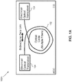
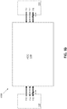
- FIGs. 1A and 1B are a structural diagram 100A and a corresponding functional diagram 100B of an example of an active optical cable (AOC) 110, according to certain aspects of the subject technology.
- the AOC 110 includes a cable (e.g., an optical cable) 102 interconnecting electrical transceivers 104 coupled to two ends of the cable 102.
- the optical cable 102 includes one or multiple optical fibers, each of which can be used for transmission of data to or reception of data from an electrical transceiver (e.g., 104).
- Each of the electrical transceivers 104 can receive an electrical signal from an electrical interface, generate an optical signal based on the electrical signal, and provide the generated optical signal to the cable 102.
- Each of the electrical transceivers 104 can simultaneously receive an optical signal from the cable 102 and generate an electrical signal to be received by the same electrical interface or another electrical interface.
- photonics and support electronics used in electrical transceivers 104 are small and low-power semiconductor devices, such that they can be located in an electrical connector back-shell.
- electrical data is first converted to an optical signal in the back-shell, transmitted over optical fiber, and then converted back to electrical data at a destination back-shell.
- box-to-box, point-to-point, optical links are accomplished with electrical only connectors to the outside of the box.
- Bidirectional links may use a dedicated fiber for each direction, or may be on a single fiber using an optical circulator approach for achieving bidirectionality.
- the AOC 110 is shown to be operable to receive power from any of the electrical interfaces (e.g., 120 and 130) that may be connected to electrical transceivers 104 through one or both of the power line 112. In some aspects, at least a portion of the received electrical power over the power lines 112 is consumed by the internal circuitry of the electrical transceivers 104.
- the control lines 114 may be used by the AOC 100 to communicate control signals with the electrical interfaces 120 and 130 connected to electrical transceivers 104.
- the control signals are electrical signals that, for example, can be utilized for controlling automatic algorithms that are responsible for performance management of the AOC 100.
- the data communication between the electrical transceivers 104 and other devices and/or systems connected to the AOC 110 through the electrical interfaces 120 and 130 is carried over the data line(s) 116 (e.g., lines 1-n, for n bits of data).
- Mechanical interfaces are also used to mechanically couple the AOC 110 to the other systems and/or devices. The mechanical interfaces are controlled for their thermal conductivity, emissivity and electromagnetic interference (EMI) qualities to make sure that a reliable thermal path and an EMI shielding are provided.
- EMI electromagnetic interference
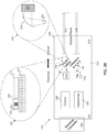
- FIGs. 2A through 2C are diagrams illustrating an example of a space AOC (SAOC) transceiver 200, according to certain aspects of the subject technology.
- the SAOC transceiver 200 is a portion of a SAOC cable, which has a similar general structure as the AOC 110 of FIG. 1A , except that all components, materials, and processes involved in the production and maintenance of the components and materials are space rated, as described herein.
- Each SAOC cable has two or more of the SAOC transceiver 200.
- the SAOC transceiver 200 can receive power, control signals, and data through the power line 112, control line 114, and the data line(s) 116, respectively.
- the electrical power received through the power line 112 is used for internal consumption by the electrical circuitry of the SAOC transceiver 200.
- the control signals are electrical signals received over the control line 114 and may be used to control the functionality and performance of the SAOC transceiver 200.
- the data received via the data line(s) 116 are electrical signals which are converted to optical signals by the SAOC transceiver 200, as further discussed below.
- the SAOC transceiver 200 as shown in FIG. 2B includes an optical portion 210 and an electrical portion 220.
- the SAOC transceiver 200 is enclosed in an enclosure 230 and is coupled to an electrical interface through an electrical connector 232 (e.g., a D-sub connector).
- the electrical interface may be an interface of a system and/or device connected to the SAOC transceiver 200 through the electrical connector 232.
- the electrical portion 220 includes a laser diode driver (LDD) 222, a trans-impedance amplifier (TIA) 224, a control circuit 226, and an electronic circuit 228.
- LDD laser diode driver
- TIA trans-impedance amplifier
- One or more lasers 204 and one or more light detectors 206 may be considered as converters between the electrical portion 220 and the optical portion 210 and are electrically coupled to the portion 220, while being optically coupled to the optical portion 210.
- the optical portion 210 includes optical components including optical couplers and/or lenses (e.g., a reflector 218) that optically couple the lasers 204 and light detectors 206 to the optical fibers (e.g., 216) of a cable (e.g., 102 of FIG. 1A ) connected to the SAOC transceiver 200.
- the optical components for the optical coupling of a laser 204 to an optical fiber 214 are shown in a blown-up view 206.
- the optical coupling of the laser 204 to the optical fiber 214 can be performed using an on-axis mount, as shown in a blown-up view 201.
- the components of the on-axis mount include a base submount 203, a vertical submount 205, the laser 204 (e.g., a VCSEL), the optical fiber 214, and, optionally, a transparent mounting block 209.
- the base submount 203 may be made, for example, of a semiconductor material such as silicon or a radiation hard and vacuum compatible printed circuit board (PCB) material.
- the vertical submount 205 may be made, for example, of alumina (Al2O3) that can support electrical traces from the laser 204 to the base submount 203.
- the transparent mounting block 209 is made, for example, of sapphire or a semiconductor material.
- the optical fiber 214 is a multi-mode fiber, although or a single-mode optical fiber can also be used instead.
- the laser 204 is mounted on the vertical submount, and the transparent mounting block 209 is not needed.
- the laser 204 may be mounted on the base submount 203, in which case the vertical mount is not used and the optical fiber 214 is mounted on a V groove created on the base submount 203 to facilitate alignment of the laser 204 with the optical fiber 207.
- the vertical mount is not used and the laser 204 is mounted on the transparent mounting block 209, which is between the laser 204 and the optical fiber 214.
- the optical coupler 218 used in the optical portion 210 is improved for achieving high optical coupling efficiency, for example, by using a first surface reflection curved instead of flat, which is critical angle dependent.
- the optical adhesive surface of the reflector 218 could be coated with a reflective material such as Au or Ag, deposition of which may further provide protection for the exposed surface.
- the surface of the reflector 218, as shown, can be further shaped or lensed and made smoother to improve coupling efficiency.
- the reflector 218 focuses the light from laser 204 into the fiber 214.
- an actively aligned separate mirror could be introduced and be held with the optical adhesive currently used.
- the disclosed optical coupling can result in significantly higher coupling efficiency. For example, using a direct alignment mount on axis with the fiber improvement in coupling efficiency of up to 70% can be achieved.
- the light detectors 206 are photodiodes properly biased to be able to detect light photons received from respective optical fibers 216 coupled to the light detectors 206.
- the light detectors 206 can generate current signals in response to the detection of light photons.
- the current signal generated by the light detectors 206 are amplified by the TIA 224, which generates corresponding voltage signals.
- the voltage signals generated by the TIA 224 are processed by the electronic circuit 228 and provided to the electrical connector 232 for transmission through the electrical interface of the system and/or device connected to the SAOC transceiver 200.
- the light detectors are coupled to fibers 216 with high efficiency couplers of the subject technology similar to the reflector 218.
- the light detectors 206 are implemented using photo-diodes, such as semiconductor photodiodes.
- the lasers 204 are vertical cavity surface-emitting laser (VCSEL) type lasers which are space rated.
- VCSEL vertical cavity surface-emitting laser
- a major advantage of VCSELs over edge-emitter lasers is ease of coupling.
- VCSELs have a circular surface output that can be coupled without the need of an additional lens to circularize to output light.
- the edge-emitting lasers may utilize a lens to help circularize the beam, have higher flux density that often requires angled coupling to avoid back reflection. Edge-emitting lasers have much higher drive current requiring more power than VCSELs.
- VCSELs may also be easily addressed as an array by an array of lenses or fibers. The VCSELs do not have mm cavity lengths and high flux density, as the edge-emitting lasers have.
- the lasers 204 may include an array of VCSELs that are coupled to and driven by the LDD 222, which is a known circuit.
- the LDD 222 is driven by signals from the electronic circuit 218 and/or the control circuit 216.
- the electronic circuit 228 receives data from data lines 116 of FIG. 2A and performs suitable processing on the received data before providing the data in the form of processed electrical signals to the LDD 222.
- the lasers 204 generate optical light (signals) for transmission over the optical fibers 214 of a cable (e.g., 102 of FIG. 1A ) connected to the SAOC transceiver 200.
- the control circuit 226 receives control signals from control lines 114 of FIG. 2A and based on the received control signals exerts control over the electronic circuit 228.
- the SAOC 200 is enclosed in the enclosure 230 with good heat-sink and EMI protection using gaskets and communicates command, control, and telemetry signals via a serial interface such as the electrical connector 232.
- Space qualification challenges may be met by leveraging space rated components such as qualified impedance-controlled electrical connectors, radiation resistant fibers and cables, radiation hard custom electronics, high reliability and high temperature VCSELs, and the like.
- the SAOC 200 may be prepared for use in radiation and vacuum environment for high-reliability space applications and may include radiation resistant fibers (e.g., resistant to gamma rays) and radiation resistant electronics (e.g., resistant to ionizing radiation, protons, and heavy ions), and space rated parts, material, and processes.
- the space rating may include making sure that the parts and material are qualified for space application with repeatable and reliable test results such having as low outgassing.
- the SAOC 200 may include automatic algorithms (e.g., routines) for autonomous device maintenance and performance management in space environments.
- the routines may be implemented in firmware and be performed by hardware, for example, one or more processors (e.g., microcontrollers such as control circuit 226 of FIG. 2B ).
- the firmware and the processors is part of the electronic circuit 228 and/or the control circuit 226.
- a space qualified electrical connector e.g., 232
- a corresponding mechanical interface is designed for vacuum pressure compatible thermal management and EMI performance.
- a Faraday cage may be used with conductive heat transfer.
- the material and components used in the SAOC 200 are selected to be operable in extended operating temperature (e.g., ⁇ 100°C at SAOC interface) and satisfy high reliability requirements of a multi-year mission use.
- the SAOC 200 may also serve as a platform 250 for RF-over-fiber, as shown FIG. 2C , or other connector back-shell based applications.
- the platform 250 of the subject technology eliminates the need for optical connectors for space applications. This is especially attractive because space applications do not have multiple bulkheads as, for example, a ship might have.
- the platform 250 provides a readily usable solution for high-speed point-to-point data links.
- the platform 250 is coupled through the interface 240 (e.g., a serial interface) to an electrical interface of another devices or system connected to the platform 250.
- the interface 240 similar to the electrical connector 232 of FIG. 2B can receive power and communicate control and data signals.
- the platform 250 includes a light source 252, local oscillator (LO) modulator 254, a radio-frequency (RF) modulator 256, and a light processor 258.
- the light source 252 includes, for example, a distributed feedback (DFB) laser, which is a type of laser diode, quantum cascade laser, or optical fiber laser with an active region that is periodically structured as a diffraction grating.
- the light source 252 generates an optical carrier signal which can be modulated with LO and RF signals, as desired.
- the LO modulator 254 receives an LO electrical signal as an input and modulates the optical carrier signal with the LO signal.
- the RF modulator 256 receives an RF electrical signal as an input and modulates the optical carrier signal with the RF signal.
- the light processor 258 includes a filter and lock-diode unit 260 and mirrors 255.
- the light processor 258 receives laser light from the DFB laser 252 and LO and RF modulated lights from the LO modulator 254 and RF modulator 256 and provides a heterodyne output light signal to an optical fiber 270 (e.g., a single-mode optical fiber).
- the filter and lock diode unit 260 includes a filter component that can filter the RF signal as desired and a wave locking laser diode that can lock the modulated laser light to the filter.
- the filter component is a multi-layer optical filter such as a wave-length-division-multiplexing (WAD) filter.
- the platform 250 may further include other RF photonics circuits including a low-noise amplifier (LNA) and one or more optical switches for routing and redundancy purposes.
- LNA low-noise amplifier
- FIGs. 3A and 3B are diagrams illustrating examples of system applications 300A and 300B of SAOC 320, according to certain aspects of the subject technology.
- one or more SAOC 320 similar to SAOC 200 of FIG. 2B may be used in digital data transfer at high date rates with strict mass and power limitations that demand an optical solution, for example, a fiber-based sensor application.
- the SAOC 320 facilitates communication between payload instruments 3 10 and a control and communication system 330. Examples of the payload instruments include GPS communication devices, earth sensor and imaging devices, and space sensor and imaging devices.
- Other applications of the SAOC include analog RF over fiber applications. In an analog RF over fiber application, as shown in FIG.
- one or more RF antennas can be coupled to an on board system processing 360 using a modified SAOC 350 such as the SAOC 250 of FIG. 2C .
- the on board system processing 360 may, for example, include RF demodulator and base-band circuitry to further process a heterodyne signal generated by the modified SAOC 350.
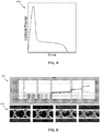
- FIG. 4 is a diagram illustrating an example of a laser pulse profile 400 used in charring the enclosure of a SAOC stopping as early as the peak (dotted line), according to certain aspects of the subject technology.
- Space hardware including SAOC e.g., 200 of FIG 2B
- nickel is one of the most desired materials for EMI performance, but has a smooth reflective surface, while high emissivity requires the use of a material with a dark or opaque finish.
- Space-rated thermal paints are often used to paint nickel black to achieve both requirements.
- Paints however, do not adhere well to nickel and have proven to flake off frequently during handling of other managed service provider (MSP) hardware, creating foreign object damage (FOD).
- MSP managed service provider
- FOD foreign object damage
- the paint option is not suitable for the SAOC because paint flakes off and as a result exposes the surface underneath. This counters the original intent of providing a uniform thermally conductive surface that enhances heat radiation.
- Kapton tape applied to the external surface of the hardware during vehicle assembly.
- the Kapton tape can raise other concerns, for example, lengthening the assembly process and changing the mass and dimensions of the hardware. It also impedes remove and replace (RandR) and raises concerns of adverse residues and appearance of the hardware.
- the subject technology improves surface emissivity, for example, of the SAOC enclosure (e.g., 230 of FIG. 2B ) by using laser charring using laser pulse profiles with controlled results.
- laser charring can be performed by applying high optical power laser profile 400 of FIG. 4 to the subject surface (e.g., nickel surface) to greatly increase absorption, and then a steep reduction in power to avoid ablating the material. Focused or diffused laser beam, laser wavelength and angle of incidence, and other factors, such as roughness of the surface, may affect the suitable laser profile for the charring process.
- the process stops at the initial charred stage, which increases the surface absorption and emissivity, assuming absorption relationship given by Kirchhoff's law of thermal radiation, while maintaining the base material properties, e.g. conductivity of nickel.
- Charring in the context of the subject disclosure is performed to change absorption properties of the surface and is not continued to result in a burnt product. It is understood that emissivity concerns radiative (e.g., with a wavelength of several microns) heat transfer, in the wavelengths beyond the visible range (unless at very high temperatures) and the results may not be evaluated based on visual appearance.
- the ease of implementing a laser charred finish, raster over most any shape surface is especially attractive, along with the permanent nature of the finish.
- FIG. 5 is a diagram illustrating plots of laser modulation currents 500 and corresponding eye diagrams 510 used in performing a health check, according to certain aspects of the subject technology.
- Existing PCB mounted optical transceivers use optical connectors to exit/enter the housing. This allows direct evaluation of optical link margin at the optical connector, but results in other challenges.
- An algorithm referred to as SAOC health check (HC) described herein allows optical link performance verification by trending bit error rate (BER) performance of the entire electrical-optical-electrical link in a configuration (e.g., an operating state) designed to yield sensitive (e.g., low margin) optical link performance with strong electrical link performance.
- BER bit error rate
- any test-to-test variation in BER performance in this operating state is directly attributable to a change in optical link performance, which may be used to evaluate the health of optical drive and optical transmission components over the system lifetime.
- the data shown in plots 500 and 510 are HC proof of concept regarding BER sensitivity.
- the plots 500 show that laser modulation currents of the VCSELS (e.g., 204 of FIG. 2B ) can be adjusted to perform health check, for example, by reducing the laser modulation currents with fixed pre-bias current (e.g., about 0.8mA) until bit error occurs.
- the laser modulation current (Imod) values are reduced from about 2.6 mA to about 1 mA.
- SAOC telemetry such as receiver signal strength indicator (RSSI) and other performance management algorithms may play roles in implementing the SAOC HC algorithm.
- RSSI receiver signal strength indicator
- other performance management algorithms may play roles in implementing the SAOC HC algorithm. Precise and repeatable control of optical performance management parameters enables trending of optical link health and performance throughout integration, test, and product life, even when the SAOC is used in a space vehicle which is on orbit.
- the SAOC optical link performance helps to detect hardware defects or issues during integration and testing stage and to understand device failure modes, preserve remaining life, and switch to redundant systems when available.
- the SAOC HC provides a measure to trend SAOC optical link performance margin using data accessible via electrical interfaces only. An established low consistent drive per end, in a loss sensitive regime, allows performance to be trended through BER and RSSI parameters.
- the BER is commonly measured in most systems, even on orbit, or can be measured using an external BER tester.
- the RSSI is related to detector photocurrent at the end of the optical link indicating a measure of optical transmission performance.
- Precise control of optical configuration is an aspect of the SAOC HC algorithm. It is known and understood that optical component performance will vary with environmental parameters (e.g., temperature). Precision sensing of the environmental parameters along with other factors such as precise and repeatable tuning of the SAOC optical drive and receiving configuration parameters for the current environment can be useful in calibrating the BER performance changes that would otherwise be attributed to these factors.
- the subject SAOC HC defines a repeatable measure of optical link performance in the SAOC configuration using data accessible via electrical interfaces.
- FIG. 6 is a flow diagram illustrating an example of an algorithm for health check (HC) of a SAOC, according to certain aspects of the subject technology.
- the HC algorithm can be implemented in firmware and be executed by hardware such one or more processors or controllers, for example, the control circuit 226 of FIG. 2B .
- the SAOC HC algorithm may be executed at multiple levels of assembly, anywhere that a pseudorandom binary sequence (PRBS) suitable for BER measurements may be generated and checked.
- PRBS pseudorandom binary sequence
- a HC configuration is determined.
- the HC configuration is determined over a planned operational environment (e.g., thermal environment) that results in an optical signal quality below a planned operational level (e.g., VCSEL drive current).
- a planned operational environment e.g., thermal environment
- a planned operational level e.g., VCSEL drive current
- the optical signal (e.g., detector photo-current) quality, measured at the receiver, is normally strong enough to avoid adverse threshold effects with an acceptable input impedance (R IN ) and bandwidth (BW) behavior, while maintaining electrical interface signal integrity margins.
- R IN input impedance
- BW bandwidth
- the acceptable R IN and BW depends on the system, for example, an acceptable values of R IN can be about 50-100 ⁇ and acceptable values of BW may in the GHz range.
- the HC configuration intentionally generates a high optical link BER and low photocurrent at the optical receiver.
- the SAOC electrical interfaces are configured using control signals to perform with full operational margin.
- BER and photocurrent measurements are taken in the HC configuration to establish baseline performance statistics for the assembly (630).
- the measurements of BER are performed repeatedly to establish performance statistics for the assembly including the SAOC.
- Test equipment and/or the flight assembly provide self-synchronizing PRBS patterns to conduct BER testing in the HC configurations. This enables HCs during integration and testing and in flight, as warranted.
- RSSI is also measured and the performance statistics includes an HC-BER and an HC-RSSI statistics for the assembly.
- BER is evaluated regularly.
- the measured BER is compared to the HC-BER. If the measured BER is not higher than that HC-BER, the assembly is in a stable condition with healthy optical links and the control is passed to the operation block 640. Otherwise, if the measured BER is higher than that HC-BER, an optical link failure is detected.
- a common laser drive condition may be used to yield in family optical BER and photocurrent.
- Each assembly may be characterized for a particular BER and photocurrent performance.
- custom laser drive condition is developed for each assembly that yields a common response and each assembly configuration is evaluated to spot outliers.
- the HC configurations are characterized over temperature to account for known optical thermal compensation effects.
- the HC configuration may be characterized coarsely over temperature, for example, using low, ambient, and high temperatures for expected effects.
- the HC configuration may be characterized finely with temperature if necessary to allow trending within family. Statistical analysis of assembly level testing and trending yields pass/fail criteria for determining in-family versus degraded assembly performance.
- the SAOC optical link signal integrity is purposely compromised in the HC configuration, but in a consistent and predictable manner necessary to obtain meaningful BER measurements and statistics.
- the SAOC HC algorithm is perceptive to drive, source, coupling, transmission, detector degradation.
- the SAOC HC is implemented for each assembled serial number to establish baseline performance statistics, and performance is trended over the life of the assembly.
- the HC configuration may be commanded throughout the life of the unit to check for changes (e.g., degradation) in optical link performance.
- BER and receiver photocurrent measurements provide perceptivity to optical source changes, fiber/coupling changes or detector degradation, even signal integrity across the electrical interface, for example, when the BER is high but photocurrent has an expected value.
- the HC approach can increase the confidence that all units are in known-good and stable states throughout and at the completion of system environmental testing and through the operational use of each optical link.
- the HC algorithm can similarly be beneficial to terrestrial AOCs that also lack an optical connector to interrogate the optical path/performance.
- FIG. 7 is a flow diagram illustrating an example of a method 700 for providing a SAOC, according to certain aspects of the subject technology.
- a cable e.g., 102 of FIG. 1A
- a first electrical transceiver e.g., 104 of FIG. 1A , or 200 of FIGs. 2A and 2B
- the first electrical transceiver is enclosed in a first enclosure (e.g., 230 of FIG. 2B ) enclosing a light detector (e.g., 206 of FIG. 2B ) and a first reflecting surface (e.g., 218 of FIG. 2B ) configured to reflect a first incident light (730).
- the first enclosure is processed to provide a predetermined heat propagation and electromagnetic interference (EMI) specification and to become radiation hard (740).
- EMI electromagnetic interference
- the cable and the first electrical transceiver are built to be radiation hard (750).
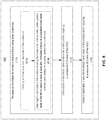
- FIG. 8 is a flow diagram illustrating an example of a method 800 for providing an AOC (e.g., 110 of FIG. 1A ), according to certain aspects of the subject technology.
- an enclosure e.g., 230 of FIG. 2B
- the charring is performed by using femto-second laser pulses, while a power level of the femto-second laser pulses are increased sharply to a predetermined-level and reduced steeply (e.g., with profile 400 of FIG. 4 ) to avoid ablating the nickel layer.
- the enclosure is used to enclose a first electrical transceiver (e.g., 200 of FIG. 2B ) for coupling to an end of the AOC.
- the first electrical transceiver includes a first optical coupler formed by a first reflector surface (e.g., similar to 218 of FIG. 2B ) and a light detector (e.g., 206 of FIG. 2B ).
- a second electrical transceiver for coupling to a opposite end of the AOC is enclosed in the enclosure similarly.
- the second electrical transceiver includes a second optical coupler formed by a second reflector surface (e.g., 218 of FIG. 2B ) and a light source (e.g., 204 of FIG. 2B ).
- compositions and methods are described in terms of “comprising,” “containing,” or “including” various components or steps, the compositions and methods can also “consist essentially of” or “consist of” the various components and operations. All numbers and ranges disclosed above can vary by some amount. Whenever a numerical range with a lower limit and an upper limit is disclosed, any number and any subrange falling within the broader range are specifically disclosed. Also, the terms in the claims have their plain, ordinary meaning unless otherwise explicitly and clearly defined by the patentee. If there is any conflict in the usages of a word or term in this specification and one or more patent or other documents that may be incorporated herein by reference, the definitions that are consistent with this specification should be adopted.
Landscapes
- Physics & Mathematics (AREA)
- General Physics & Mathematics (AREA)
- Optics & Photonics (AREA)
- Electromagnetism (AREA)
- Engineering & Computer Science (AREA)
- Computer Networks & Wireless Communication (AREA)
- Signal Processing (AREA)
- Optical Couplings Of Light Guides (AREA)
Claims (15)
- Weltraumtaugliches aktives optisches Kabel (SAOC) (200, 250, 350), umfassend:ein Kabel (102), das einen oder mehrere Lichtwellenleiter umfasst; undzwei oder mehrere elektrische Transceiver (104) an entgegengesetzten Enden des Kabels (102) und durch das Kabel (102) miteinander verbunden, wobei jeder der elektrischen Transceiver (104) von den zwei oder mehreren elektrischen Transceivern (104) umfasst:
ein Gehäuse (230), umfassend:eine oder mehrere Lichtquellen (252), einen oder mehrere Lichtdetektoren (206) und Steuerelektronik, die in dem Gehäuse eingeschlossen sind; undein Kopplungsmedium, das dazu eingerichtet ist, Licht in den einen oder die mehreren Lichtwellenleiter einzukoppeln und aus ihm bzw. ihnen auszukoppeln,einen Hochfrequenz- (HF) -Modulator (256) und einen Lokaloszillator- (LO) - Modulator (254), die dazu eingerichtet sind, Licht zu modulieren, das von der einen oder den mehreren Lichtquellen erzeugt wird; und
einen Lichtprozessor (258), der mit der einen oder den mehreren Lichtquellen (252), dem HF-Modulator (256) und dem LO-Modulator (254) gekoppelt ist und eine Filter- und Sperr-Diodeneinheit (260) umfasst, die dazu eingerichtet ist, ein heterodynes Ausgangslicht zu erzeugen, und wobei das Gehäuse eine geeignete Wärmeausbreitung und Abschirmung gegen elektromagnetische Störung bereitstellt und das Kabel und die zwei oder mehreren elektrischen Transceiver strahlungsbeständig sind. - SAOC (200, 250, 350) nach Anspruch 1, wobei jeder der elektrischen Transceiver (104) eine weltraumtaugliche elektrische Schnittstelle umfasst, die dazu eingerichtet ist, Strom (112) zu empfangen und Signale zu übermitteln, die Daten- (116), Befehls-, Steuer- (114) und Telemetriesignale umfassen, wobei jede Lichtquelle (252) der einen oder mehreren Lichtquellen (252) dazu eingerichtet ist, ein empfangenes (RX) elektrisches Signal in Licht umzuwandeln, und wobei jeder Lichtdetektor (206) des einen oder der mehreren Lichtdetektoren (206) dazu eingerichtet ist, empfangenes Licht gleichzeitig mit der Umwandlung des elektrischen RX-Signals in ein elektrisches Signal umzuwandeln.
- SAOC (200, 250, 350) nach Anspruch 1, wobei das Kopplungsmedium eine reflektierende Oberfläche (218) umfasst, wobei jeder der elektrischen Transceiver (104) dazu eingerichtet ist, eine geformte reflektierende Oberfläche (218) zu verwenden, um Licht von jeder Lichtquelle (204) der einen oder mehreren Lichtquellen in einen Lichtwellenleiter (214) zu fokussieren und gleichzeitig empfangenes Licht von einem Lichtwellenleiter (216) des einen oder der mehreren Lichtwellenleiter in einen Lichtdetektor (206) des einen oder der mehreren Lichtdetektoren zu fokussieren.
- SAOC (200, 250, 350) nach Anspruch 1, wobei das Kabel und der eine oder die mehreren elektrischen Transceiver (104) unter Verwendung von weltraumtauglichen Bauteilen, Materialien und Prozessen gebaut sind, wobei die weltraumtauglichen Bauteile, Materialien und Prozesse auf Vakuumverträglichkeit und Zuverlässigkeit qualitätsgeprüft sind, wobei das Kopplungsmedium eine Halterung in der optischen Achse umfasst, wobei jede Lichtquelle der einen oder mehreren Lichtquellen einen weltraumtrauglichen Oberflächenemitter (VCSEL) umfasst und wobei der weltraumtaugliche VCSEL auf Strahlungsbeständigkeit und Zuverlässigkeit qualitätsgeprüft ist.
- SAOC (200, 250, 350) nach Anspruch 1, wobei das Gehäuse (230) unter Verwendung von kurzen Laserpulsen derart bearbeitet ist, dass es eine Laser-geschwärzte Oberfläche aufweist, um Absorption und Emissionsgrad zu erhöhen, wobei die kurzen Laserpulse dazu eingerichtet sind, eine geschwärzte Oberfläche zu erzeugen, die wärmeleitend ist, wobei das Kopplungsmedium eine reflektierende Oberfläche umfasst und wobei die reflektierende Oberfläche durch Formen und/oder Beschichten mit einem reflektierenden Material verbessert ist, um die optische Kopplungseffizienz zu steigern und die reflektierende Oberfläche zu schützen.
- SAOC (200, 250, 350) nach Anspruch 1, wobei bei jedem der elektrischen Transceiver (200) eine eigenständige Steuerung der Ausgestaltung von elektrischen und optischen Bauelementen zur Leistungserhaltung in Weltraumumgebungen durch Abschwächung von Temperatur- und Strahlungseinflüssen vorgesehen ist, wobei jeder der elektrische Transceiver (104) die Trenddarstellung der optischen Leistung ohne optische Anschlüsse ermöglicht und wobei die Trenddarstellung der optischen Leistung unter Verwendung der Bitfehlerrate (BER) und des Indikators für die empfangene Signalstärke (RSSI) bei einem empfindlich niedrigen Ansteuerregime des VCSEL realisiert wird.
- SAOC nach Anspruch 6, wobei die Trenddarstellung der optischen Leistung während einer Lebensdauer des SAOC bewerkstelligt wird, indem nur elektrische Schnittstellen in einer Health-Check- (HC) -Konfiguration verwendet werden, die wahrnehmungsfähig für optische Verluste ist, wobei die HC-Konfiguration mit einem optischen Ansteuerpegel je Teil mit annehmbaren Eigenschaften festgelegt ist, die Ausgangssignalstärke und Bandbreite für nominell wiederholbare BER und RSSI umfassen.
- Verfahren zum Bereitstellen eines weltraumtauglichen aktiven optischen Kabels (SAOC) (200, 250, 350), wobei das Verfahren umfasst:Bereitstellen eines Kabels (102), das einen oder mehrere Lichtwellenleiter umfasst;Bereitstellen eines ersten elektrischen Transceivers (104) zum Koppeln mit einem ersten Ende des Kabels (102);Einschließen des ersten elektrischen Transceivers (104) in ein erstes Gehäuse (230), umfassend- eine Lichtquelle (252), einen Lichtdetektor (206) und eine erste reflektierende Oberfläche (218), die dazu eingerichtet ist, ein erstes einfallendes Licht zu reflektieren;- einen Hochfrequenz- (HF) -Modulator (256) und einen Lokaloszillator- (LO) - Modulator (254), die dazu eingerichtet sind, Licht zu modulieren, das von der Lichtquelle (252) erzeugt wird; undeinen Lichtprozessor (258), der mit der Lichtquelle (252), dem HF-Modulator (256) und dem LO-Modulator (254) gekoppelt ist und eine Filter- und Sperr-Diodeneinheit (260) umfasst, die dazu eingerichtet ist, ein heterodynes Ausgangslicht zu erzeugen, und Bearbeiten des ersten Gehäuses, um eine geeignete Wärmeausbreitung und Spezifikation für die elektromagnetische Störung bereitzustellen; und Vorsehen der Strahlungsbeständigkeit des Kabels und der ersten elektrischen Transceiver.
- Verfahren nach Anspruch 8, ferner umfassend:Einrichten des Lichtdetektors (206) dazu, ein reflektiertes Licht in ein übertragenes (TX) elektrisches Signal umzuwandeln, undEinrichten der ersten reflektierenden Oberfläche (218) dazu, das reflektierte Licht durch Reflektieren des ersten einfallenden Lichts von dem einen oder den mehreren Lichtwellenleitern zu erzeugen.
- Verfahren nach Anspruch 8, ferner umfassend:Bereitstellen eines zweiten elektrischen Transceivers (104), der mit einem zweiten Ende des Kabels (102) gekoppelt ist; undEinschließen des zweiten elektrischen Transceivers (104) in ein zweites Gehäuse (230), das eine Lichtquelle (252) und eine zweite reflektierende Oberfläche (218) umfasst, die dazu eingerichtet ist, ein zweites einfallendes Licht zu reflektieren.
- Verfahren nach Anspruch 10, wobei das Bearbeiten des ersten Gehäuses (230) das Bereitstellen einer Laser-geschwärzten Oberfläche unter Verwendung von Femtosekunden-Laserpulsen umfasst, wobei das zweite Gehäuse (230) in ähnlicher Weise wie das erste Gehäuse (230) bearbeitet wird und wobei das Verfahren ferner das Formen der ersten reflektierenden Oberfläche (218) und der zweiten reflektierenden Oberfläche (218) und das Beschichten mit einem reflektierenden Material umfasst, das Gold oder Silber umfasst, um die optische Kopplungseffizienz zu steigern.
- Verfahren nach Anspruch 10, wobei das Bereitstellen des ersten elektrischen Transceivers (104) und des zweiten elektrischen Transceivers (104) automatische Konfigurationsalgorithmen umfasst, die einen Health-Check- (HC) -Prozess zum Bewerten der optischen Leistung unter Verwendung elektrischer Schnittstellen unter Verwendung der Bitfehlerrate (BER) und eines Indikators für die empfangene Signalstärke (RSSI) in einem empfindlich niedrigen Ansteuerregime umfassen.
- Verfahren nach Anspruch 12, wobei der HC-Prozess das Bestimmen einer HC-Konfiguration über einer geplanten thermischen Betriebsumgebung umfasst, die in einer Qualität des optischen Signals unterhalb eines geplanten Betriebsniveaus resultiert, wobei die Qualität des optischen Signals ausreichend gut ist, um nachteilige Schwelleneffekte mit einer annehmbaren Eingangsimpedanz (RIN) und einem annehmbaren Bandbreiten- (BW) -Verhalten zu vermeiden und zugleich Signalintegritätsspannen der elektrischen Schnittstelle aufrechtzuerhalten.
- Verfahren nach Anspruch 13, wobei der HC-Prozess ferner umfasst:Durchführen wiederholter Messungen der Bitfehlerrate (BER) und des Indikators für die empfangene Signalstärke (RSSI), um Leistungsstatistiken für das SAOC aufzustellen, wobei die Leistungsstatistiken eine HC-BER- und eine HC-RSSI-Statistik umfassen;in einem Kontext eines integrierten Systems, Wiederholen der HC-BER- und HC-RSSI-Messungen, um Systemleistungsstatistiken aufzustellen, die eine System-HC-BER und einen System-HC-RSSI umfassen; undüber ein Betriebsleben des integrierten Systems, Messen der BER und des RSSI und Erfassen einer Fehlfunktion oder Verschlechterung der optischen Verbindung durch Vergleichen der gemessenen BER und des gemessenen RSSI mit der System-HC-BER und dem System-HC-RSSI, undwobei der HC-Prozess auf allgemein implementierte aktive optische Kabel zusätzlich zu dem SAOC angewendet wird.
- Verfahren zum Bereitstellen eines aktiven optischen Kabels (AOC) (110), wobei das Verfahren umfasst:
Bearbeiten eines Gehäuses zum Erzeugen einer geschwärzten Oberfläche unter Verwendung von Laserpulsen durch:Ausbilden einer Nickelschicht über Oberflächen des Gehäuses; undSchwärzen der Oberflächen des Gehäuses unter Verwendung von Femtosekunden-Laserpulsen, während ein Energieniveau der Femtosekunden-Laserpulse scharf auf ein vorgegebenes Niveau angehoben und steil verringert wird, um ein Abschmelzen der Nickelschicht zu verhindern; undVerwendung des Gehäuses zum Einschließen eines ersten elektrischen Transceivers (104) zum Koppeln mit einem Übertragungs- (TX) -Ende des AOC,
wobei:ein zweiter elektrischer Transceiver (104) zum Koppeln mit einem Empfangs- (RX) -Ende des AOC in ähnlicher Weise eingeschlossen ist,der erste elektrische Transceiver (104) einen ersten Optokoppler umfasst, der von einer ersten Spiegelfläche (218) und einem Lichtdetektor (206) gebildet wird, undder zweite elektrische Transceiver (104) einen zweiten Optokoppler umfasst, der von einer zweiten Spiegelfläche (218) und einer Lichtquelle (252) gebildet wird.
Applications Claiming Priority (3)
| Application Number | Priority Date | Filing Date | Title |
|---|---|---|---|
| US201562161767P | 2015-05-14 | 2015-05-14 | |
| US15/150,254 US20160334591A1 (en) | 2015-05-14 | 2016-05-09 | Space active optical cable |
| PCT/US2016/031767 WO2016183142A1 (en) | 2015-05-14 | 2016-05-11 | Space active optical cable |
Publications (3)
| Publication Number | Publication Date |
|---|---|
| EP3295233A1 EP3295233A1 (de) | 2018-03-21 |
| EP3295233A4 EP3295233A4 (de) | 2019-01-23 |
| EP3295233B1 true EP3295233B1 (de) | 2020-07-01 |
Family
ID=57249512
Family Applications (1)
| Application Number | Title | Priority Date | Filing Date |
|---|---|---|---|
| EP16793406.6A Active EP3295233B1 (de) | 2015-05-14 | 2016-05-11 | Raumaktives optisches kabel |
Country Status (4)
| Country | Link |
|---|---|
| US (5) | US20160334591A1 (de) |
| EP (1) | EP3295233B1 (de) |
| CA (2) | CA2997730C (de) |
| WO (1) | WO2016183142A1 (de) |
Families Citing this family (7)
| Publication number | Priority date | Publication date | Assignee | Title |
|---|---|---|---|---|
| US20160334591A1 (en) | 2015-05-14 | 2016-11-17 | Lockheed Martin Corporation | Space active optical cable |
| US10598871B2 (en) * | 2016-05-11 | 2020-03-24 | Inneos LLC | Active optical cable for wearable device display |
| US10454579B1 (en) * | 2016-05-11 | 2019-10-22 | Zephyr Photonics Inc. | Active optical cable for helmet mounted displays |
| US10551309B2 (en) | 2016-07-22 | 2020-02-04 | Comodo Security Solutions, Inc. | Method and system to improve scheme of optical network cable and audio cable |
| US11515629B2 (en) * | 2020-04-24 | 2022-11-29 | Reflex Photonics Inc. | Radiation tolerant electro-optical devices for communication in space |
| CN114137670A (zh) * | 2020-09-03 | 2022-03-04 | 英业达科技有限公司 | 电子组件及光通信元件 |
| US11677473B2 (en) * | 2021-07-09 | 2023-06-13 | Brian D. Morrison | Hybrid wire-fiber data networks for electromagnetic and/or ground-noise environments, components thereof, and systems incorporating same |
Family Cites Families (29)
| Publication number | Priority date | Publication date | Assignee | Title |
|---|---|---|---|---|
| US3731225A (en) * | 1962-04-02 | 1973-05-01 | Sanders Associates Inc | Fiber optic laser system |
| US4021834A (en) * | 1975-12-31 | 1977-05-03 | The United States Of America As Represented By The Secretary Of The Army | Radiation-resistant integrated optical signal communicating device |
| JPS61204609A (ja) * | 1985-03-07 | 1986-09-10 | Power Reactor & Nuclear Fuel Dev Corp | イメージファイバ |
| US5047835A (en) * | 1989-12-26 | 1991-09-10 | At&T Bell Laboratories | Lightwave packaging for pairs of optical devices |
| US5828476A (en) * | 1996-06-11 | 1998-10-27 | The Boeing Company | Dual rate, burst mode, radiation hardened, optical transceiver |
| US20020027689A1 (en) * | 2000-09-05 | 2002-03-07 | Meir Bartur | Fiber optic transceiver employing front end level control |
| US6659655B2 (en) * | 2001-02-12 | 2003-12-09 | E20 Communications, Inc. | Fiber-optic modules with housing/shielding |
| US6786651B2 (en) * | 2001-03-22 | 2004-09-07 | Primarion, Inc. | Optical interconnect structure, system and transceiver including the structure, and method of forming the same |
| US20030138251A1 (en) * | 2001-10-12 | 2003-07-24 | Harish Jayaram | Method and system for performance monitoring in an optical network |
| KR100896405B1 (ko) * | 2001-12-14 | 2009-05-08 | 레어드 테크놀로지스 인코포레이티드 | 손실성 매체를 포함하는 emi 쉴딩 |
| US6788540B2 (en) * | 2002-01-30 | 2004-09-07 | Jds Uniphase Corporation | Optical transceiver cage |
| US7448802B2 (en) * | 2002-02-20 | 2008-11-11 | Newton Scientific, Inc. | Integrated X-ray source module |
| US7484899B2 (en) * | 2006-11-01 | 2009-02-03 | The Boeing Company | Small-form-factor fiber optic transceiver module having built-in test capability and method |
| CN101983127B (zh) * | 2008-04-04 | 2014-07-09 | Nok株式会社 | 氟橡胶-金属层合垫片材料 |
| FR2943337B1 (fr) * | 2009-03-20 | 2011-12-23 | Draka Comteq France | Procede de traitement de fibres optiques au deuterium |
| US20110268390A1 (en) * | 2010-05-01 | 2011-11-03 | Avago Technologies Fiber Ip (Singapore) Pte. Ltd. | Active optical cable that is suited for consumer applications and a method |
| CN103140787A (zh) * | 2010-09-12 | 2013-06-05 | 安费诺-图赫尔电子有限公司 | 光学联接装置、光电子构件和光电子收发器 |
| DK2431778T3 (en) * | 2010-09-17 | 2017-01-16 | Gigoptix-Helix Ag | Flexible configurable optical subunit |
| US8403571B2 (en) * | 2010-12-07 | 2013-03-26 | Corning Cable Systems Llc | Apparatuses, systems, and methods for facilitating optical communication between electronic devices |
| US8534931B2 (en) * | 2011-01-25 | 2013-09-17 | Avago Technologies General Ip (Singapore) Pte. Ltd. | Active optical cable (AOC) and a method and apparatus for performing power management in the AOC |
| TWI465784B (zh) * | 2011-11-23 | 2014-12-21 | Via Tech Inc | 主動型光纖纜線與電子裝置 |
| US9160451B2 (en) * | 2012-03-06 | 2015-10-13 | Sae Magnetics (H.K.) Ltd. | Active optical cable connector plug and active optical cable using same |
| US8872723B2 (en) | 2012-07-13 | 2014-10-28 | Senaya, Inc. | Light and RF transparent enclosure for use with asset tracking device |
| US9160452B2 (en) * | 2012-12-29 | 2015-10-13 | Zephyr Photonics Inc. | Apparatus for modular implementation of multi-function active optical cables |
| US9321638B2 (en) * | 2013-01-09 | 2016-04-26 | Savannah River Nuclear Solutions, Llc | Use of triphenyl phosphate as risk mitigant for metal amide hydrogen storage materials |
| US9563028B2 (en) * | 2013-01-31 | 2017-02-07 | Ccs Technology, Inc. | Method to manufacture an optoelectronic assembly |
| US8876413B2 (en) * | 2013-03-14 | 2014-11-04 | Avago Technologies General Ip (Singapore) Pte. Ltd. | Method and system for providing electromagnetic interference (EMI) shielding in an optical communications module |
| US9351055B2 (en) * | 2013-08-15 | 2016-05-24 | Mellanox Technologies Ltd. | High-reliability active optical cable (AOC) with redundant emitters |
| US20160334591A1 (en) | 2015-05-14 | 2016-11-17 | Lockheed Martin Corporation | Space active optical cable |
-
2016
- 2016-05-09 US US15/150,254 patent/US20160334591A1/en not_active Abandoned
- 2016-05-11 CA CA2997730A patent/CA2997730C/en active Active
- 2016-05-11 CA CA3254095A patent/CA3254095A1/en active Pending
- 2016-05-11 EP EP16793406.6A patent/EP3295233B1/de active Active
- 2016-05-11 WO PCT/US2016/031767 patent/WO2016183142A1/en not_active Ceased
-
2019
- 2019-09-24 US US16/581,560 patent/US10690865B2/en active Active
-
2020
- 2020-06-22 US US16/907,968 patent/US11709326B2/en active Active
-
2023
- 2023-07-25 US US18/225,902 patent/US12001069B2/en active Active
-
2024
- 2024-03-26 US US18/617,647 patent/US12523829B2/en active Active
Non-Patent Citations (1)
| Title |
|---|
| None * |
Also Published As
| Publication number | Publication date |
|---|---|
| CA3254095A1 (en) | 2025-06-14 |
| US11709326B2 (en) | 2023-07-25 |
| US20200018913A1 (en) | 2020-01-16 |
| EP3295233A1 (de) | 2018-03-21 |
| US10690865B2 (en) | 2020-06-23 |
| US20160334591A1 (en) | 2016-11-17 |
| US20240264391A1 (en) | 2024-08-08 |
| EP3295233A4 (de) | 2019-01-23 |
| US20240027704A1 (en) | 2024-01-25 |
| CA2997730A1 (en) | 2016-11-17 |
| WO2016183142A1 (en) | 2016-11-17 |
| US20200333541A1 (en) | 2020-10-22 |
| CA2997730C (en) | 2026-03-17 |
| US12523829B2 (en) | 2026-01-13 |
| US12001069B2 (en) | 2024-06-04 |
Similar Documents
| Publication | Publication Date | Title |
|---|---|---|
| US12001069B2 (en) | Space active optical cable | |
| KR100921566B1 (ko) | 모듈식 광 트랜시버 | |
| US6863453B2 (en) | Method and apparatus for parallel optical transceiver module assembly | |
| KR101880070B1 (ko) | 광 도파관을 통한 동시의 데이터 및 전력 전송을 위한 장치 | |
| EP1918747B1 (de) | Faseroptisches Sende- und Empfangsmodul mit kleinem Formfaktor und eingebauter Testfähigkeit sowie Verfahren | |
| US9547142B1 (en) | Optical transmitter module | |
| US7309169B2 (en) | Single-channel communication device for optical fibre | |
| TWI850219B (zh) | 有整合的光纖耦合器之單一波長雙向收發器 | |
| Gilli et al. | New prospects of optical wireless communication systems exploiting VCSEL-based transmitters | |
| US10754111B1 (en) | Method for modifying small form factor pluggable transceiver for avionics applications | |
| RU2717374C2 (ru) | Субблок оптической скамьи с интегрированным фотонным устройством | |
| US7463830B2 (en) | Modular optical transmitter for WWDM transceivers | |
| Kurata et al. | Achieving high reliability in silicon photonics optical transceivers for harsh environments over 100° C in excess of 10 year operation | |
| Masuko et al. | A low cost PON transceiver using single TO-CAN type micro-BOSA | |
| US8023784B1 (en) | Optical subassembly package configuration | |
| US20090060529A1 (en) | Optical bench fiber optic transmitter | |
| Nagashima et al. | 1060-nm VCSEL-based 28-Gb/s× 4-channnel optical signal transmission beyond 500-m MMF using high-density parallel-optical modules | |
| Nga et al. | 10 Gbps/ch Full-Duplex Optical Link Using a Single-Fiber Channel for Signal Transmission | |
| RU195171U1 (ru) | Оптоэлектронный модуль | |
| Beranek | Future generation military avionics fiber optics photonics packaging challenges | |
| Ménager et al. | Optically remoted probe for sensing of RF in aerospace radars | |
| Ashton et al. | Semiconductor cw laser packages with full hermeticity integral power monitoring and direct fibre optic launching | |
| Bristow et al. | Advancement of photonic interconnects for spaceborne systems | |
| Lauzon et al. | Highly-hermetic feedthrough fiber pigtailed circular TO-can electro-optic sensor for avionics applications | |
| Langenwalter et al. | Fiber-Optic Transceivers |
Legal Events
| Date | Code | Title | Description |
|---|---|---|---|
| STAA | Information on the status of an ep patent application or granted ep patent |
Free format text: STATUS: THE INTERNATIONAL PUBLICATION HAS BEEN MADE |
|
| PUAI | Public reference made under article 153(3) epc to a published international application that has entered the european phase |
Free format text: ORIGINAL CODE: 0009012 |
|
| STAA | Information on the status of an ep patent application or granted ep patent |
Free format text: STATUS: REQUEST FOR EXAMINATION WAS MADE |
|
| 17P | Request for examination filed |
Effective date: 20171204 |
|
| AK | Designated contracting states |
Kind code of ref document: A1 Designated state(s): AL AT BE BG CH CY CZ DE DK EE ES FI FR GB GR HR HU IE IS IT LI LT LU LV MC MK MT NL NO PL PT RO RS SE SI SK SM TR |
|
| AX | Request for extension of the european patent |
Extension state: BA ME |
|
| DAV | Request for validation of the european patent (deleted) | ||
| DAX | Request for extension of the european patent (deleted) | ||
| A4 | Supplementary search report drawn up and despatched |
Effective date: 20181220 |
|
| RIC1 | Information provided on ipc code assigned before grant |
Ipc: G02B 6/42 20060101AFI20181214BHEP Ipc: H04B 10/40 20130101ALI20181214BHEP |
|
| GRAP | Despatch of communication of intention to grant a patent |
Free format text: ORIGINAL CODE: EPIDOSNIGR1 |
|
| STAA | Information on the status of an ep patent application or granted ep patent |
Free format text: STATUS: GRANT OF PATENT IS INTENDED |
|
| INTG | Intention to grant announced |
Effective date: 20191126 |
|
| GRAS | Grant fee paid |
Free format text: ORIGINAL CODE: EPIDOSNIGR3 |
|
| GRAA | (expected) grant |
Free format text: ORIGINAL CODE: 0009210 |
|
| STAA | Information on the status of an ep patent application or granted ep patent |
Free format text: STATUS: THE PATENT HAS BEEN GRANTED |
|
| AK | Designated contracting states |
Kind code of ref document: B1 Designated state(s): AL AT BE BG CH CY CZ DE DK EE ES FI FR GB GR HR HU IE IS IT LI LT LU LV MC MK MT NL NO PL PT RO RS SE SI SK SM TR |
|
| REG | Reference to a national code |
Ref country code: CH Ref legal event code: EP Ref country code: AT Ref legal event code: REF Ref document number: 1286702 Country of ref document: AT Kind code of ref document: T Effective date: 20200715 |
|
| REG | Reference to a national code |
Ref country code: IE Ref legal event code: FG4D |
|
| REG | Reference to a national code |
Ref country code: DE Ref legal event code: R096 Ref document number: 602016039196 Country of ref document: DE |
|
| REG | Reference to a national code |
Ref country code: LT Ref legal event code: MG4D |
|
| PG25 | Lapsed in a contracting state [announced via postgrant information from national office to epo] |
Ref country code: BG Free format text: LAPSE BECAUSE OF FAILURE TO SUBMIT A TRANSLATION OF THE DESCRIPTION OR TO PAY THE FEE WITHIN THE PRESCRIBED TIME-LIMIT Effective date: 20201001 |
|
| REG | Reference to a national code |
Ref country code: NL Ref legal event code: MP Effective date: 20200701 |
|
| REG | Reference to a national code |
Ref country code: AT Ref legal event code: MK05 Ref document number: 1286702 Country of ref document: AT Kind code of ref document: T Effective date: 20200701 |
|
| PG25 | Lapsed in a contracting state [announced via postgrant information from national office to epo] |
Ref country code: LT Free format text: LAPSE BECAUSE OF FAILURE TO SUBMIT A TRANSLATION OF THE DESCRIPTION OR TO PAY THE FEE WITHIN THE PRESCRIBED TIME-LIMIT Effective date: 20200701 Ref country code: AT Free format text: LAPSE BECAUSE OF FAILURE TO SUBMIT A TRANSLATION OF THE DESCRIPTION OR TO PAY THE FEE WITHIN THE PRESCRIBED TIME-LIMIT Effective date: 20200701 Ref country code: HR Free format text: LAPSE BECAUSE OF FAILURE TO SUBMIT A TRANSLATION OF THE DESCRIPTION OR TO PAY THE FEE WITHIN THE PRESCRIBED TIME-LIMIT Effective date: 20200701 Ref country code: GR Free format text: LAPSE BECAUSE OF FAILURE TO SUBMIT A TRANSLATION OF THE DESCRIPTION OR TO PAY THE FEE WITHIN THE PRESCRIBED TIME-LIMIT Effective date: 20201002 Ref country code: NO Free format text: LAPSE BECAUSE OF FAILURE TO SUBMIT A TRANSLATION OF THE DESCRIPTION OR TO PAY THE FEE WITHIN THE PRESCRIBED TIME-LIMIT Effective date: 20201001 Ref country code: SE Free format text: LAPSE BECAUSE OF FAILURE TO SUBMIT A TRANSLATION OF THE DESCRIPTION OR TO PAY THE FEE WITHIN THE PRESCRIBED TIME-LIMIT Effective date: 20200701 Ref country code: FI Free format text: LAPSE BECAUSE OF FAILURE TO SUBMIT A TRANSLATION OF THE DESCRIPTION OR TO PAY THE FEE WITHIN THE PRESCRIBED TIME-LIMIT Effective date: 20200701 Ref country code: PT Free format text: LAPSE BECAUSE OF FAILURE TO SUBMIT A TRANSLATION OF THE DESCRIPTION OR TO PAY THE FEE WITHIN THE PRESCRIBED TIME-LIMIT Effective date: 20201102 Ref country code: ES Free format text: LAPSE BECAUSE OF FAILURE TO SUBMIT A TRANSLATION OF THE DESCRIPTION OR TO PAY THE FEE WITHIN THE PRESCRIBED TIME-LIMIT Effective date: 20200701 Ref country code: CZ Free format text: LAPSE BECAUSE OF FAILURE TO SUBMIT A TRANSLATION OF THE DESCRIPTION OR TO PAY THE FEE WITHIN THE PRESCRIBED TIME-LIMIT Effective date: 20200701 |
|
| PG25 | Lapsed in a contracting state [announced via postgrant information from national office to epo] |
Ref country code: LV Free format text: LAPSE BECAUSE OF FAILURE TO SUBMIT A TRANSLATION OF THE DESCRIPTION OR TO PAY THE FEE WITHIN THE PRESCRIBED TIME-LIMIT Effective date: 20200701 Ref country code: PL Free format text: LAPSE BECAUSE OF FAILURE TO SUBMIT A TRANSLATION OF THE DESCRIPTION OR TO PAY THE FEE WITHIN THE PRESCRIBED TIME-LIMIT Effective date: 20200701 Ref country code: RS Free format text: LAPSE BECAUSE OF FAILURE TO SUBMIT A TRANSLATION OF THE DESCRIPTION OR TO PAY THE FEE WITHIN THE PRESCRIBED TIME-LIMIT Effective date: 20200701 Ref country code: IS Free format text: LAPSE BECAUSE OF FAILURE TO SUBMIT A TRANSLATION OF THE DESCRIPTION OR TO PAY THE FEE WITHIN THE PRESCRIBED TIME-LIMIT Effective date: 20201101 |
|
| PG25 | Lapsed in a contracting state [announced via postgrant information from national office to epo] |
Ref country code: NL Free format text: LAPSE BECAUSE OF FAILURE TO SUBMIT A TRANSLATION OF THE DESCRIPTION OR TO PAY THE FEE WITHIN THE PRESCRIBED TIME-LIMIT Effective date: 20200701 |
|
| REG | Reference to a national code |
Ref country code: DE Ref legal event code: R097 Ref document number: 602016039196 Country of ref document: DE |
|
| PG25 | Lapsed in a contracting state [announced via postgrant information from national office to epo] |
Ref country code: RO Free format text: LAPSE BECAUSE OF FAILURE TO SUBMIT A TRANSLATION OF THE DESCRIPTION OR TO PAY THE FEE WITHIN THE PRESCRIBED TIME-LIMIT Effective date: 20200701 Ref country code: DK Free format text: LAPSE BECAUSE OF FAILURE TO SUBMIT A TRANSLATION OF THE DESCRIPTION OR TO PAY THE FEE WITHIN THE PRESCRIBED TIME-LIMIT Effective date: 20200701 Ref country code: EE Free format text: LAPSE BECAUSE OF FAILURE TO SUBMIT A TRANSLATION OF THE DESCRIPTION OR TO PAY THE FEE WITHIN THE PRESCRIBED TIME-LIMIT Effective date: 20200701 Ref country code: IT Free format text: LAPSE BECAUSE OF FAILURE TO SUBMIT A TRANSLATION OF THE DESCRIPTION OR TO PAY THE FEE WITHIN THE PRESCRIBED TIME-LIMIT Effective date: 20200701 Ref country code: SM Free format text: LAPSE BECAUSE OF FAILURE TO SUBMIT A TRANSLATION OF THE DESCRIPTION OR TO PAY THE FEE WITHIN THE PRESCRIBED TIME-LIMIT Effective date: 20200701 |
|
| PLBE | No opposition filed within time limit |
Free format text: ORIGINAL CODE: 0009261 |
|
| STAA | Information on the status of an ep patent application or granted ep patent |
Free format text: STATUS: NO OPPOSITION FILED WITHIN TIME LIMIT |
|
| PG25 | Lapsed in a contracting state [announced via postgrant information from national office to epo] |
Ref country code: AL Free format text: LAPSE BECAUSE OF FAILURE TO SUBMIT A TRANSLATION OF THE DESCRIPTION OR TO PAY THE FEE WITHIN THE PRESCRIBED TIME-LIMIT Effective date: 20200701 |
|
| 26N | No opposition filed |
Effective date: 20210406 |
|
| PG25 | Lapsed in a contracting state [announced via postgrant information from national office to epo] |
Ref country code: SK Free format text: LAPSE BECAUSE OF FAILURE TO SUBMIT A TRANSLATION OF THE DESCRIPTION OR TO PAY THE FEE WITHIN THE PRESCRIBED TIME-LIMIT Effective date: 20200701 |
|
| PG25 | Lapsed in a contracting state [announced via postgrant information from national office to epo] |
Ref country code: SI Free format text: LAPSE BECAUSE OF FAILURE TO SUBMIT A TRANSLATION OF THE DESCRIPTION OR TO PAY THE FEE WITHIN THE PRESCRIBED TIME-LIMIT Effective date: 20200701 |
|
| REG | Reference to a national code |
Ref country code: CH Ref legal event code: PL |
|
| PG25 | Lapsed in a contracting state [announced via postgrant information from national office to epo] |
Ref country code: CH Free format text: LAPSE BECAUSE OF NON-PAYMENT OF DUE FEES Effective date: 20210531 Ref country code: LU Free format text: LAPSE BECAUSE OF NON-PAYMENT OF DUE FEES Effective date: 20210511 Ref country code: MC Free format text: LAPSE BECAUSE OF FAILURE TO SUBMIT A TRANSLATION OF THE DESCRIPTION OR TO PAY THE FEE WITHIN THE PRESCRIBED TIME-LIMIT Effective date: 20200701 Ref country code: LI Free format text: LAPSE BECAUSE OF NON-PAYMENT OF DUE FEES Effective date: 20210531 |
|
| REG | Reference to a national code |
Ref country code: BE Ref legal event code: MM Effective date: 20210531 |
|
| PG25 | Lapsed in a contracting state [announced via postgrant information from national office to epo] |
Ref country code: IE Free format text: LAPSE BECAUSE OF NON-PAYMENT OF DUE FEES Effective date: 20210511 |
|
| PG25 | Lapsed in a contracting state [announced via postgrant information from national office to epo] |
Ref country code: BE Free format text: LAPSE BECAUSE OF NON-PAYMENT OF DUE FEES Effective date: 20210531 |
|
| PG25 | Lapsed in a contracting state [announced via postgrant information from national office to epo] |
Ref country code: HU Free format text: LAPSE BECAUSE OF FAILURE TO SUBMIT A TRANSLATION OF THE DESCRIPTION OR TO PAY THE FEE WITHIN THE PRESCRIBED TIME-LIMIT; INVALID AB INITIO Effective date: 20160511 |
|
| PG25 | Lapsed in a contracting state [announced via postgrant information from national office to epo] |
Ref country code: CY Free format text: LAPSE BECAUSE OF FAILURE TO SUBMIT A TRANSLATION OF THE DESCRIPTION OR TO PAY THE FEE WITHIN THE PRESCRIBED TIME-LIMIT Effective date: 20200701 |
|
| PG25 | Lapsed in a contracting state [announced via postgrant information from national office to epo] |
Ref country code: MK Free format text: LAPSE BECAUSE OF FAILURE TO SUBMIT A TRANSLATION OF THE DESCRIPTION OR TO PAY THE FEE WITHIN THE PRESCRIBED TIME-LIMIT Effective date: 20200701 |
|
| PG25 | Lapsed in a contracting state [announced via postgrant information from national office to epo] |
Ref country code: TR Free format text: LAPSE BECAUSE OF FAILURE TO SUBMIT A TRANSLATION OF THE DESCRIPTION OR TO PAY THE FEE WITHIN THE PRESCRIBED TIME-LIMIT Effective date: 20200701 |
|
| PG25 | Lapsed in a contracting state [announced via postgrant information from national office to epo] |
Ref country code: MT Free format text: LAPSE BECAUSE OF FAILURE TO SUBMIT A TRANSLATION OF THE DESCRIPTION OR TO PAY THE FEE WITHIN THE PRESCRIBED TIME-LIMIT Effective date: 20200701 |
|
| PGFP | Annual fee paid to national office [announced via postgrant information from national office to epo] |
Ref country code: FR Payment date: 20250310 Year of fee payment: 10 |
|
| PGFP | Annual fee paid to national office [announced via postgrant information from national office to epo] |
Ref country code: GB Payment date: 20250320 Year of fee payment: 10 |
|
| PGFP | Annual fee paid to national office [announced via postgrant information from national office to epo] |
Ref country code: DE Payment date: 20250319 Year of fee payment: 10 |