EP3296044B1 - Oberflächenbeschichtetes schneidwerkzeug - Google Patents
Oberflächenbeschichtetes schneidwerkzeug Download PDFInfo
- Publication number
- EP3296044B1 EP3296044B1 EP15882293.2A EP15882293A EP3296044B1 EP 3296044 B1 EP3296044 B1 EP 3296044B1 EP 15882293 A EP15882293 A EP 15882293A EP 3296044 B1 EP3296044 B1 EP 3296044B1
- Authority
- EP
- European Patent Office
- Prior art keywords
- layer
- base material
- residual stress
- coating
- thickness
- Prior art date
- Legal status (The legal status is an assumption and is not a legal conclusion. Google has not performed a legal analysis and makes no representation as to the accuracy of the status listed.)
- Active
Links
Images


Classifications
-
- C—CHEMISTRY; METALLURGY
- C01—INORGANIC CHEMISTRY
- C01F—COMPOUNDS OF THE METALS BERYLLIUM, MAGNESIUM, ALUMINIUM, CALCIUM, STRONTIUM, BARIUM, RADIUM, THORIUM, OR OF THE RARE-EARTH METALS
- C01F7/00—Compounds of aluminium
- C01F7/02—Aluminium oxide; Aluminium hydroxide; Aluminates
-
- C—CHEMISTRY; METALLURGY
- C23—COATING METALLIC MATERIAL; COATING MATERIAL WITH METALLIC MATERIAL; CHEMICAL SURFACE TREATMENT; DIFFUSION TREATMENT OF METALLIC MATERIAL; COATING BY VACUUM EVAPORATION, BY SPUTTERING, BY ION IMPLANTATION OR BY CHEMICAL VAPOUR DEPOSITION, IN GENERAL; INHIBITING CORROSION OF METALLIC MATERIAL OR INCRUSTATION IN GENERAL
- C23C—COATING METALLIC MATERIAL; COATING MATERIAL WITH METALLIC MATERIAL; SURFACE TREATMENT OF METALLIC MATERIAL BY DIFFUSION INTO THE SURFACE, BY CHEMICAL CONVERSION OR SUBSTITUTION; COATING BY VACUUM EVAPORATION, BY SPUTTERING, BY ION IMPLANTATION OR BY CHEMICAL VAPOUR DEPOSITION, IN GENERAL
- C23C30/00—Coating with metallic material characterised only by the composition of the metallic material, i.e. not characterised by the coating process
- C23C30/005—Coating with metallic material characterised only by the composition of the metallic material, i.e. not characterised by the coating process on hard metal substrates
-
- B—PERFORMING OPERATIONS; TRANSPORTING
- B23—MACHINE TOOLS; METAL-WORKING NOT OTHERWISE PROVIDED FOR
- B23B—TURNING; BORING
- B23B27/00—Tools for turning or boring machines; Tools of a similar kind in general; Accessories therefor
- B23B27/14—Cutting tools of which the bits or tips or cutting inserts are of special material
- B23B27/148—Composition of the cutting inserts
-
- C—CHEMISTRY; METALLURGY
- C04—CEMENTS; CONCRETE; ARTIFICIAL STONE; CERAMICS; REFRACTORIES
- C04B—LIME, MAGNESIA; SLAG; CEMENTS; COMPOSITIONS THEREOF, e.g. MORTARS, CONCRETE OR LIKE BUILDING MATERIALS; ARTIFICIAL STONE; CERAMICS; REFRACTORIES; TREATMENT OF NATURAL STONE
- C04B37/00—Joining burned ceramic articles with other burned ceramic articles or other articles by heating
- C04B37/001—Joining burned ceramic articles with other burned ceramic articles or other articles by heating directly with other burned ceramic articles
-
- C—CHEMISTRY; METALLURGY
- C04—CEMENTS; CONCRETE; ARTIFICIAL STONE; CERAMICS; REFRACTORIES
- C04B—LIME, MAGNESIA; SLAG; CEMENTS; COMPOSITIONS THEREOF, e.g. MORTARS, CONCRETE OR LIKE BUILDING MATERIALS; ARTIFICIAL STONE; CERAMICS; REFRACTORIES; TREATMENT OF NATURAL STONE
- C04B37/00—Joining burned ceramic articles with other burned ceramic articles or other articles by heating
- C04B37/003—Joining burned ceramic articles with other burned ceramic articles or other articles by heating by means of an interlayer consisting of a combination of materials selected from glass, or ceramic material with metals, metal oxides or metal salts
- C04B37/005—Joining burned ceramic articles with other burned ceramic articles or other articles by heating by means of an interlayer consisting of a combination of materials selected from glass, or ceramic material with metals, metal oxides or metal salts consisting of glass or ceramic material
-
- C—CHEMISTRY; METALLURGY
- C23—COATING METALLIC MATERIAL; COATING MATERIAL WITH METALLIC MATERIAL; CHEMICAL SURFACE TREATMENT; DIFFUSION TREATMENT OF METALLIC MATERIAL; COATING BY VACUUM EVAPORATION, BY SPUTTERING, BY ION IMPLANTATION OR BY CHEMICAL VAPOUR DEPOSITION, IN GENERAL; INHIBITING CORROSION OF METALLIC MATERIAL OR INCRUSTATION IN GENERAL
- C23C—COATING METALLIC MATERIAL; COATING MATERIAL WITH METALLIC MATERIAL; SURFACE TREATMENT OF METALLIC MATERIAL BY DIFFUSION INTO THE SURFACE, BY CHEMICAL CONVERSION OR SUBSTITUTION; COATING BY VACUUM EVAPORATION, BY SPUTTERING, BY ION IMPLANTATION OR BY CHEMICAL VAPOUR DEPOSITION, IN GENERAL
- C23C16/00—Chemical coating by decomposition of gaseous compounds, without leaving reaction products of surface material in the coating, i.e. chemical vapour deposition [CVD] processes
- C23C16/02—Pretreatment of the material to be coated
- C23C16/0272—Deposition of sub-layers, e.g. to promote the adhesion of the main coating
-
- C—CHEMISTRY; METALLURGY
- C23—COATING METALLIC MATERIAL; COATING MATERIAL WITH METALLIC MATERIAL; CHEMICAL SURFACE TREATMENT; DIFFUSION TREATMENT OF METALLIC MATERIAL; COATING BY VACUUM EVAPORATION, BY SPUTTERING, BY ION IMPLANTATION OR BY CHEMICAL VAPOUR DEPOSITION, IN GENERAL; INHIBITING CORROSION OF METALLIC MATERIAL OR INCRUSTATION IN GENERAL
- C23C—COATING METALLIC MATERIAL; COATING MATERIAL WITH METALLIC MATERIAL; SURFACE TREATMENT OF METALLIC MATERIAL BY DIFFUSION INTO THE SURFACE, BY CHEMICAL CONVERSION OR SUBSTITUTION; COATING BY VACUUM EVAPORATION, BY SPUTTERING, BY ION IMPLANTATION OR BY CHEMICAL VAPOUR DEPOSITION, IN GENERAL
- C23C16/00—Chemical coating by decomposition of gaseous compounds, without leaving reaction products of surface material in the coating, i.e. chemical vapour deposition [CVD] processes
- C23C16/22—Chemical coating by decomposition of gaseous compounds, without leaving reaction products of surface material in the coating, i.e. chemical vapour deposition [CVD] processes characterised by the deposition of inorganic material, other than metallic material
- C23C16/30—Deposition of compounds, mixtures or solid solutions, e.g. borides, carbides, nitrides
- C23C16/40—Oxides
- C23C16/403—Oxides of aluminium, magnesium or beryllium
-
- C—CHEMISTRY; METALLURGY
- C23—COATING METALLIC MATERIAL; COATING MATERIAL WITH METALLIC MATERIAL; CHEMICAL SURFACE TREATMENT; DIFFUSION TREATMENT OF METALLIC MATERIAL; COATING BY VACUUM EVAPORATION, BY SPUTTERING, BY ION IMPLANTATION OR BY CHEMICAL VAPOUR DEPOSITION, IN GENERAL; INHIBITING CORROSION OF METALLIC MATERIAL OR INCRUSTATION IN GENERAL
- C23C—COATING METALLIC MATERIAL; COATING MATERIAL WITH METALLIC MATERIAL; SURFACE TREATMENT OF METALLIC MATERIAL BY DIFFUSION INTO THE SURFACE, BY CHEMICAL CONVERSION OR SUBSTITUTION; COATING BY VACUUM EVAPORATION, BY SPUTTERING, BY ION IMPLANTATION OR BY CHEMICAL VAPOUR DEPOSITION, IN GENERAL
- C23C16/00—Chemical coating by decomposition of gaseous compounds, without leaving reaction products of surface material in the coating, i.e. chemical vapour deposition [CVD] processes
- C23C16/56—After-treatment
-
- C—CHEMISTRY; METALLURGY
- C23—COATING METALLIC MATERIAL; COATING MATERIAL WITH METALLIC MATERIAL; CHEMICAL SURFACE TREATMENT; DIFFUSION TREATMENT OF METALLIC MATERIAL; COATING BY VACUUM EVAPORATION, BY SPUTTERING, BY ION IMPLANTATION OR BY CHEMICAL VAPOUR DEPOSITION, IN GENERAL; INHIBITING CORROSION OF METALLIC MATERIAL OR INCRUSTATION IN GENERAL
- C23C—COATING METALLIC MATERIAL; COATING MATERIAL WITH METALLIC MATERIAL; SURFACE TREATMENT OF METALLIC MATERIAL BY DIFFUSION INTO THE SURFACE, BY CHEMICAL CONVERSION OR SUBSTITUTION; COATING BY VACUUM EVAPORATION, BY SPUTTERING, BY ION IMPLANTATION OR BY CHEMICAL VAPOUR DEPOSITION, IN GENERAL
- C23C28/00—Coating for obtaining at least two superposed coatings either by methods not provided for in a single one of groups C23C2/00 - C23C26/00 or by combinations of methods provided for in subclasses C23C and C25C or C25D
- C23C28/04—Coating for obtaining at least two superposed coatings either by methods not provided for in a single one of groups C23C2/00 - C23C26/00 or by combinations of methods provided for in subclasses C23C and C25C or C25D only coatings of inorganic non-metallic material
- C23C28/044—Coating for obtaining at least two superposed coatings either by methods not provided for in a single one of groups C23C2/00 - C23C26/00 or by combinations of methods provided for in subclasses C23C and C25C or C25D only coatings of inorganic non-metallic material coatings specially adapted for cutting tools or wear applications
-
- B—PERFORMING OPERATIONS; TRANSPORTING
- B23—MACHINE TOOLS; METAL-WORKING NOT OTHERWISE PROVIDED FOR
- B23B—TURNING; BORING
- B23B2224/00—Materials of tools or workpieces composed of a compound including a metal
- B23B2224/04—Aluminium oxide
-
- B—PERFORMING OPERATIONS; TRANSPORTING
- B23—MACHINE TOOLS; METAL-WORKING NOT OTHERWISE PROVIDED FOR
- B23B—TURNING; BORING
- B23B2224/00—Materials of tools or workpieces composed of a compound including a metal
- B23B2224/28—Titanium carbide
-
- B—PERFORMING OPERATIONS; TRANSPORTING
- B23—MACHINE TOOLS; METAL-WORKING NOT OTHERWISE PROVIDED FOR
- B23B—TURNING; BORING
- B23B2224/00—Materials of tools or workpieces composed of a compound including a metal
- B23B2224/32—Titanium carbide nitride (TiCN)
-
- B—PERFORMING OPERATIONS; TRANSPORTING
- B23—MACHINE TOOLS; METAL-WORKING NOT OTHERWISE PROVIDED FOR
- B23B—TURNING; BORING
- B23B2224/00—Materials of tools or workpieces composed of a compound including a metal
- B23B2224/36—Titanium nitride
-
- B—PERFORMING OPERATIONS; TRANSPORTING
- B23—MACHINE TOOLS; METAL-WORKING NOT OTHERWISE PROVIDED FOR
- B23B—TURNING; BORING
- B23B2228/00—Properties of materials of tools or workpieces, materials of tools or workpieces applied in a specific manner
- B23B2228/04—Properties of materials of tools or workpieces, materials of tools or workpieces applied in a specific manner applied by chemical vapour deposition [CVD]
-
- B—PERFORMING OPERATIONS; TRANSPORTING
- B23—MACHINE TOOLS; METAL-WORKING NOT OTHERWISE PROVIDED FOR
- B23B—TURNING; BORING
- B23B2228/00—Properties of materials of tools or workpieces, materials of tools or workpieces applied in a specific manner
- B23B2228/08—Properties of materials of tools or workpieces, materials of tools or workpieces applied in a specific manner applied by physical vapour deposition [PVD]
-
- B—PERFORMING OPERATIONS; TRANSPORTING
- B23—MACHINE TOOLS; METAL-WORKING NOT OTHERWISE PROVIDED FOR
- B23B—TURNING; BORING
- B23B2228/00—Properties of materials of tools or workpieces, materials of tools or workpieces applied in a specific manner
- B23B2228/10—Coatings
- B23B2228/105—Coatings with specified thickness
-
- B—PERFORMING OPERATIONS; TRANSPORTING
- B23—MACHINE TOOLS; METAL-WORKING NOT OTHERWISE PROVIDED FOR
- B23B—TURNING; BORING
- B23B2228/00—Properties of materials of tools or workpieces, materials of tools or workpieces applied in a specific manner
- B23B2228/36—Multi-layered
-
- B—PERFORMING OPERATIONS; TRANSPORTING
- B23—MACHINE TOOLS; METAL-WORKING NOT OTHERWISE PROVIDED FOR
- B23C—MILLING
- B23C2228/00—Properties of materials of tools or workpieces, materials of tools or workpieces applied in a specific manner
- B23C2228/10—Coating
-
- C—CHEMISTRY; METALLURGY
- C01—INORGANIC CHEMISTRY
- C01P—INDEXING SCHEME RELATING TO STRUCTURAL AND PHYSICAL ASPECTS OF SOLID INORGANIC COMPOUNDS
- C01P2002/00—Crystal-structural characteristics
- C01P2002/70—Crystal-structural characteristics defined by measured X-ray, neutron or electron diffraction data
- C01P2002/78—Crystal-structural characteristics defined by measured X-ray, neutron or electron diffraction data by stacking-plane distances or stacking sequences
-
- C—CHEMISTRY; METALLURGY
- C04—CEMENTS; CONCRETE; ARTIFICIAL STONE; CERAMICS; REFRACTORIES
- C04B—LIME, MAGNESIA; SLAG; CEMENTS; COMPOSITIONS THEREOF, e.g. MORTARS, CONCRETE OR LIKE BUILDING MATERIALS; ARTIFICIAL STONE; CERAMICS; REFRACTORIES; TREATMENT OF NATURAL STONE
- C04B2237/00—Aspects relating to ceramic laminates or to joining of ceramic articles with other articles by heating
- C04B2237/02—Aspects relating to interlayers, e.g. used to join ceramic articles with other articles by heating
- C04B2237/04—Ceramic interlayers
- C04B2237/08—Non-oxidic interlayers
-
- C—CHEMISTRY; METALLURGY
- C04—CEMENTS; CONCRETE; ARTIFICIAL STONE; CERAMICS; REFRACTORIES
- C04B—LIME, MAGNESIA; SLAG; CEMENTS; COMPOSITIONS THEREOF, e.g. MORTARS, CONCRETE OR LIKE BUILDING MATERIALS; ARTIFICIAL STONE; CERAMICS; REFRACTORIES; TREATMENT OF NATURAL STONE
- C04B2237/00—Aspects relating to ceramic laminates or to joining of ceramic articles with other articles by heating
- C04B2237/02—Aspects relating to interlayers, e.g. used to join ceramic articles with other articles by heating
- C04B2237/04—Ceramic interlayers
- C04B2237/08—Non-oxidic interlayers
- C04B2237/083—Carbide interlayers, e.g. silicon carbide interlayers
-
- C—CHEMISTRY; METALLURGY
- C04—CEMENTS; CONCRETE; ARTIFICIAL STONE; CERAMICS; REFRACTORIES
- C04B—LIME, MAGNESIA; SLAG; CEMENTS; COMPOSITIONS THEREOF, e.g. MORTARS, CONCRETE OR LIKE BUILDING MATERIALS; ARTIFICIAL STONE; CERAMICS; REFRACTORIES; TREATMENT OF NATURAL STONE
- C04B2237/00—Aspects relating to ceramic laminates or to joining of ceramic articles with other articles by heating
- C04B2237/30—Composition of layers of ceramic laminates or of ceramic or metallic articles to be joined by heating, e.g. Si substrates
- C04B2237/32—Ceramic
- C04B2237/34—Oxidic
- C04B2237/343—Alumina or aluminates
-
- C—CHEMISTRY; METALLURGY
- C04—CEMENTS; CONCRETE; ARTIFICIAL STONE; CERAMICS; REFRACTORIES
- C04B—LIME, MAGNESIA; SLAG; CEMENTS; COMPOSITIONS THEREOF, e.g. MORTARS, CONCRETE OR LIKE BUILDING MATERIALS; ARTIFICIAL STONE; CERAMICS; REFRACTORIES; TREATMENT OF NATURAL STONE
- C04B2237/00—Aspects relating to ceramic laminates or to joining of ceramic articles with other articles by heating
- C04B2237/30—Composition of layers of ceramic laminates or of ceramic or metallic articles to be joined by heating, e.g. Si substrates
- C04B2237/32—Ceramic
- C04B2237/36—Non-oxidic
-
- C—CHEMISTRY; METALLURGY
- C04—CEMENTS; CONCRETE; ARTIFICIAL STONE; CERAMICS; REFRACTORIES
- C04B—LIME, MAGNESIA; SLAG; CEMENTS; COMPOSITIONS THEREOF, e.g. MORTARS, CONCRETE OR LIKE BUILDING MATERIALS; ARTIFICIAL STONE; CERAMICS; REFRACTORIES; TREATMENT OF NATURAL STONE
- C04B2237/00—Aspects relating to ceramic laminates or to joining of ceramic articles with other articles by heating
- C04B2237/50—Processing aspects relating to ceramic laminates or to the joining of ceramic articles with other articles by heating
- C04B2237/70—Forming laminates or joined articles comprising layers of a specific, unusual thickness
- C04B2237/704—Forming laminates or joined articles comprising layers of a specific, unusual thickness of one or more of the ceramic layers or articles
-
- C—CHEMISTRY; METALLURGY
- C04—CEMENTS; CONCRETE; ARTIFICIAL STONE; CERAMICS; REFRACTORIES
- C04B—LIME, MAGNESIA; SLAG; CEMENTS; COMPOSITIONS THEREOF, e.g. MORTARS, CONCRETE OR LIKE BUILDING MATERIALS; ARTIFICIAL STONE; CERAMICS; REFRACTORIES; TREATMENT OF NATURAL STONE
- C04B2237/00—Aspects relating to ceramic laminates or to joining of ceramic articles with other articles by heating
- C04B2237/50—Processing aspects relating to ceramic laminates or to the joining of ceramic articles with other articles by heating
- C04B2237/70—Forming laminates or joined articles comprising layers of a specific, unusual thickness
- C04B2237/708—Forming laminates or joined articles comprising layers of a specific, unusual thickness of one or more of the interlayers
-
- C—CHEMISTRY; METALLURGY
- C04—CEMENTS; CONCRETE; ARTIFICIAL STONE; CERAMICS; REFRACTORIES
- C04B—LIME, MAGNESIA; SLAG; CEMENTS; COMPOSITIONS THEREOF, e.g. MORTARS, CONCRETE OR LIKE BUILDING MATERIALS; ARTIFICIAL STONE; CERAMICS; REFRACTORIES; TREATMENT OF NATURAL STONE
- C04B2237/00—Aspects relating to ceramic laminates or to joining of ceramic articles with other articles by heating
- C04B2237/50—Processing aspects relating to ceramic laminates or to the joining of ceramic articles with other articles by heating
- C04B2237/72—Forming laminates or joined articles comprising at least two interlayers directly next to each other
-
- C—CHEMISTRY; METALLURGY
- C04—CEMENTS; CONCRETE; ARTIFICIAL STONE; CERAMICS; REFRACTORIES
- C04B—LIME, MAGNESIA; SLAG; CEMENTS; COMPOSITIONS THEREOF, e.g. MORTARS, CONCRETE OR LIKE BUILDING MATERIALS; ARTIFICIAL STONE; CERAMICS; REFRACTORIES; TREATMENT OF NATURAL STONE
- C04B2237/00—Aspects relating to ceramic laminates or to joining of ceramic articles with other articles by heating
- C04B2237/50—Processing aspects relating to ceramic laminates or to the joining of ceramic articles with other articles by heating
- C04B2237/76—Forming laminates or joined articles comprising at least one member in the form other than a sheet or disc, e.g. two tubes or a tube and a sheet or disc
Definitions
- the present invention relates to a surface-coated cutting tool.
- a surface-coated cutting tool having a coating formed on a base material has conventionally been used.
- Japanese Patent Laying-Open No. 2004-284003 discloses a surface-coated cutting tool having a coating including an ⁇ -Al 2 O 3 layer in which a total area of crystal grains showing a crystal orientation of a (0001) plane is 70% or higher when viewed in a direction of normal to a surface of the layer in a plan view.
- Japanese Patent Laying-Open No. 2010-207946 discloses a surface-coated cutting tool having a coating including an ⁇ -Al 2 O 3 layer in which crystal grains observed at a surface have a specific size range when viewed in a direction of normal to a surface of the layer in a plan view.
- Document US 2014/287210 A1 relates to a surface-coated cutting tool with a hard coating layer exhibiting an excellent flaking and chipping resistance in a high-speed heavy and intermittent cutting is provided.
- the vapor-deposited hard coating layer has a lower layer (Ti compound layer) and an upper layer ( ⁇ -type Al2O3 layer). Thirty to 70% of Al2O3 crystal grains directly above the lower layer are oriented to (11-20) plane. Forty-five % or more of all of the Al2O3 crystal grains are oriented to (0001) plane.
- the outermost surface layer of the lower layer is an oxygen-containing TiCN layer having oxygen content of 0.5 to 3 atomic % only within the depth region of 500 nm n.
- the ratio of the number of Al2O3 crystal grains directly above the outermost surface layer to the number of crystal grains of the Ti carbonitride layer in the outermost surface layer is 0.01 to 0.5 in the interface.
- Document US 2009/297835 A1 relates to a coated cutting tool (1) including a substrate (8) and a coating (9) formed on the substrate (8), wherein the coating (9) includes a first coating (10) composed of TiCN and a second coating (ii)composed of alpha-Al2O3, the first coating (10) is positioned between the substrate (8) and the second coating (11) and has tensile stress S1, the second coating (11) has compressive stress S2, and the tensile stress S1 and the compressive stress S2 are defined by the following equation (I): 400 MPa ⁇
- Document JP 2009/184046 A relates to a surface coated cutting tool has: a lower layer comprising an adhesive Ti compound layer and a reformed TiCN layer; and an upper layer comprising a reformed [alphal-type aluminum oxide layer, which are formed by vapor deposition on a surface of a tool substrate.
- lower-layer ⁇ 3 correspondence grain boundaries amounting to 30 to 70% of the lower-layer ⁇ 3 correspondence grain boundaries existing in an upper-layer to lower-layer interface of the adhesive Ti compound layer or reformed TiCN layer existing adjacent to the upper layer form grain boundaries, continue with upper-layer ⁇ 3 coincidence grain boundaries.
- Document JP 2011/235414 A relates to a surface-coated cutting tool is obtained by depositing a Ti compound layer as a lower layer (a), an ⁇ -AlO layer as an intermediate layer (b) and an ⁇ -AlO-layer which has crystal grain structures of a flat-plate polygonal shape and a longitudinally long shape and includes B, as an upper layer (c) on the surface of a tool base body.
- the intermediate layer includes the ⁇ -AlO having the maximum sharp peak within 0-10° inclination angle and a high frequency ratio within the range of 0-10° inclination angle in an inclination angle frequency distribution graph.
- the upper layer includes the ⁇ -AlO containing B.
- the inside of each of crystal grains of ⁇ 60% by area ratio of crystal grains of the upper layer is divided by a crystal lattice interface comprised of a constituent atom sharing lattice point form expressed by at least one ⁇ 3.
- the present disclosure was made in view of such circumstances, and an object thereof is to provide a surface-coated cutting tool achieving improved mechanical characteristics of a coating and longer life of the cutting tool.
- a surface-coated cutting tool is a surface-coated cutting tool including a base material and a coating formed on the base material, the coating has an ⁇ -Al 2 O 3 layer containing a plurality of crystal grains of ⁇ -Al 2 O 3 , and the ⁇ -Al 2 O 3 layer includes a lower layer portion which is located on a base material side in a thickness direction and has a thickness of 1 ⁇ m and an upper layer portion which is located on a surface side opposite to the base material side and has a thickness of 2 ⁇ m.
- the ⁇ -Al 2 O 3 layer has a stress distribution varying in the thickness direction, the surface side of the ⁇ -Al 2 O 3 layer has a compressive residual stress, and the base material side of the ⁇ -Al 2 O 3 layer has a tensile residual stress. In this case, the surface-coated cutting tool is further longer in life.
- Embodiments of the present invention will initially be listed and described.
- an individual plane is shown in ().
- Denotation "A to B” herein means an upper limit and a lower limit of a range (that is, not less than A and not more than B), and when a unit is specified not for A but only for B, the unit is common to A and B.
- a chemical formula such as "TiN” or "TiCN” in which an atomic ratio is not particularly specified herein does not indicate that an atomic ratio of each element is limited only to "1" but encompasses all conventionally known atomic ratios.
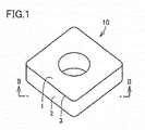
- a surface-coated cutting tool 10 has a rake face 1, a flank face 2, and a cutting edge ridgeline portion 3 at which rake face 1 and flank face 2 intersect with each other.
- rake face 1 and flank face 2 are surfaces connected to each other with cutting edge ridgeline portion 3 being interposed
- Cutting edge ridgeline portion 3 implements a cutting edge tip end portion of tool 10.
- Such a shape of tool 10 relies on a shape of a base material which will be described later.
- Fig. 1 shows tool 10 representing a throwaway chip for turning
- tool 10 is not limited thereto and the tool can suitably be used as a cutting tool such as a drill, an end mill, a throwaway tip for a drill, a throwaway tip for an end mill, a throwaway tip for milling, a metal saw, a gear cutting tool, a reamer, and a tap.
- tool 10 When tool 10 is implemented as a throwaway chip, tool 10 may or may not have a chip breaker, and cutting edge ridgeline portion 3 may have a sharp edge (a ridge at which a rake face and a flank face intersect with each other), may be honed (a sharp edge provided with R), may have a negative land (beveled), and may be honed and have a negative land.
- tool 10 has a base material 11 and a coating 12 formed on base material 11.
- coating 12 preferably covers the entire surface of base material 11 in tool 10, a part of base material 11 being not covered with coating 12 or a partially different construction of coating 12 does not depart from the scope of the present embodiment.
- base material 1 I has a rake face 11a, a flank face 11b, and a cutting edge ridgeline portion 11c at which rake face 11 a and flank face 11b intersect with each other.
- Rake face 11a, flank face 11b, and cutting edge ridgeline portion 11c implement rake face 1, flank face 2, and cutting edge ridgeline portion 3 of tool 10, respectively.
- any conventionally known base material of such a kind can be employed.
- Such a base material is preferably exemplified by cemented carbide (for example, WC-based cemented carbide, which contains not only WC but also Co, or to which a carbonitride of Ti, Ta, or Nb may be added), cermet (mainly composed of TiC, TiN, or TiCN), high-speed steel, ceramics (titanium carbide, silicon carbide, silicon nitride, aluminum nitride, or aluminum oxide), a cubic boron nitride sintered object, or a diamond sintered object.
- cemented carbide for example, WC-based cemented carbide, which contains not only WC but also Co, or to which a carbonitride of Ti, Ta, or Nb may be added
- cermet mainly composed of TiC, TiN, or TiCN
- high-speed steel ceramics (titanium carbide, silicon carbide, silicon nitride, aluminum nitride, or aluminum oxide), a cubic boron nitride
- Coating 12 includes at least one ⁇ -Al 2 O 3 layer which will be described below in detail.
- Coating 12 can include other layers so long as it includes an ⁇ -Al 2 O 3 layer.
- a composition of other layers is not particularly limited, and examples thereof can include TiC, TiN, TiB, TiBN, TiAIN, TiSiN, AlCrN, TiA1SiN, TiAINO, AlCrSiCN, TiCN, TiCNO, TiSiC, CrSiN, AlTiSiCO, or TiSiCN.
- An order of layering is not particularly limited either.
- Such coating 12 has a function to improve various characteristics such as resistance to wear and resistance to breakage by covering base material 11.
- Coating 12 has a thickness preferably from 3 to 35 ⁇ m. When coating 12 has a thickness not smaller than 3 ⁇ m, shorter life of the tool due to a small thickness of coating 12 is suppressed. When coating 12 has a thickness not greater than 35 ⁇ m, resistance to breakage in an early stage of cutting is improved.
- Coating 12 in which an underlying layer 13, a first intermediate layer 14, a second intermediate layer 15, and an ⁇ -Al 2 O 3 layer 16 are successively stacked from a base material side toward a surface side of coating 12 (upward from below in the figure) representing one example of a preferred construction of coating 12 according to the present embodiment will be described with reference to Fig. 3 .
- Alpha-Al 2 O 3 ) layer 16 in the present embodiment is a layer containing a plurality of crystal grains of ⁇ -Al 2 O 3 (aluminum oxide of which crystal structure is of an ⁇ type) Namely, this layer is composed of polycrystalline ⁇ -Al 2 O 3 . Normally, these crystal grains have a grain size approximately from 50 to 3000 nm.
- Alpha-Al 2 O 3 layer 16 in the present embodiment satisfies the following requirements
- Alpha-Al 2 O 3 layer 16 includes a lower layer portion which is located on a base material side in a thickness direction and has a thickness of 1 ⁇ m and an upper layer portion which is located on a surface side opposite to the base material side and has a thickness of 2 ⁇ m.
- a lower surface 16b of ⁇ -Al 2 O 3 ] layer 16 shown in Fig. 4 is a surface located on a side of base material 11 in Fig. 3 , that is, a surface in contact with second intermediate layer 15, and an upper surface 16a is a surface located on a surface side of coating 12 opposite to the side of base material 11, that is, the surface of ⁇ -Al 2 O 3 layer 16
- a surface in contact with the surface layer is defined as upper surface 16a.
- an ⁇ -Al 2 O 3 ] layer is formed based on a manufacturing method which will be described later. Then, the formed ( ⁇ -Al 2 O 3 layer (including the base material) is cut to obtain a cross-section perpendicular to the ⁇ -Al 2 O 3 layer (that is, cut to expose a cut surface obtained by cutting the ⁇ -Al 2 O 3 layer along a plane including a normal line to the surface of the ⁇ -Al 2 O 3 layer). Thereafter, the cut surface is polished with water resistant sandpaper (which contains an SiC grain abrasive as an abrasive).
- water resistant sandpaper which contains an SiC grain abrasive as an abrasive
- the ⁇ -Al 2 O 3 layer is cut, for example, in such a manner that the surface of ⁇ -Al 2 O 3 layer 16 (when another layer is formed on ⁇ -Al 2 O 3 layer 16, a surface of the coating) is fixed with the use of wax or the like as being in intimate contact to a sufficiently large flat plate for holding, and thereafter the ⁇ -Al 2 O 3 layer is cut in a direction perpendicular to the flat plate with a cutter with a rotary blade (cut such that the rotary blade and the flat plate are as perpendicular as possible to each other).
- Any portion af ⁇ -Al 2 O 3 layer 16 can be cut so long as the ⁇ -Al 2 O 3 layer is cut in such a perpendicular direction, however, a portion in the vicinity of the cutting edge ridgeline portion is preferably cut as will be described later.
- Polishing is performed successively with water resistant sandpaper #400, #800, and #1500 (the number (#) of the water resistant sandpaper means a difference in grain size of the abrasive, and a greater number indicates a smaller grain size of the abrasive).
- the polished surface is further smoothened through ion milling treatment with the use of Ar ions.
- Conditions for ion milling treatment are as follows.
- Irradiation angle 0° from a direction of normal to the surface of the ⁇ -Al 2 O 3 layer (that is, a linear direction in parallel to a direction of thickness of the ⁇ -Al 2 O 3 layer at the cut surface)
- a smoothened cross-section (mirrored surface) is observed with an FE-SEM with EBSD (a product name: "SU6600" manufactured by Hitachi High-Technologies Corporation), and the obtained observation image is subjected to EBSD analyses.
- a location of observation is not particularly limited, a portion in the vicinity of the cutting edge ridgeline portion is preferably observed in consideration of relation with cutting characteristics.
- EBSD analyses data is successively collected by individually positioning focused electron beams onto each pixel.
- a normal line to a sample surface (a smoothened cross-section of the ⁇ -Al 2 O 3 layer) is inclined by 70° with respect to incident beams, and analysis is conducted at 15 kV.
- a pressure of 10 Pa is applied,
- a high current mode is set in conformity with a diameter of an opening of 60 ⁇ m or 120 ⁇ m.
- Data is collected stepwise at 0.1 ⁇ m/step, for 500 ⁇ 300 points corresponding to a plane region of 50x30 ⁇ m on the cross-section.
- results of EBSD analyses are analyzed by using commercially available software (a trademark: "orientation Imaging microscopy Ver 6.2" manufactured by EDAX Inc.) and a color map is created. Specifically, a crystal orientation A of each crystal grain included in a cross-section of ( ⁇ -Al 2 O 3 layer 16 is specified. Crystal orientation A of each crystal grain specified here is a plane orientation observed when each crystal grain which appears in the cross-section of ⁇ -Al 2 O 3 layer 16 is two-dimensionally viewed in a direction of normal to the cross-section (a direction passing through the sheet surface in Fig. 4 ). A plane orientation of each crystal grain in the direction of normal to the surface of ⁇ -Al 2 O 3 layer 16 is then specified based on obtained crystal orientation A of each crystal grain.
- a color map is created based on the specified plane orientation.
- the technique according to "Crystal Direction MAP" included in the software can be used for creating a color map.
- the color map is created over the entire region of ⁇ -Al 2 O 3 layer 16 observed in the cut surface.
- each hatched region surrounded by a solid line represents a (001) plane orientation crystal grain
- each region surrounded by a solid line and not hatched represents a crystal grain of which direction of normal to the (001) plane is in a direction other than the former.
- crystal grains of which plane orientation in the direction of normal to the surface of ⁇ -Al 2 O 3 layer 16 is the (001) plane and a surface displaced from the (001) plane by 10° or smaller are hatched, and crystal grains of which plane orientation in the direction of normal to the surface of ⁇ -Al 2 O 3 layer 16 is a surface other than the former are not hatched.
- a region shown in black in Fig. 4 is regarded as a region of crystal grains of which crystal orientation has not been specified with the method above.
- a linear dimension (a shortest distance) d 1 from a virtual straight line S1 toward the base material of ⁇ -Al 2 O 3 layer 16 is 2 ⁇ m, which is a thickness of upper layer portion 16A.
- a linear dimension (a shortest distance) d 2 from a virtual straight line S2 toward the surface of ⁇ -Al 2 O 3 layer 16 is 1 ⁇ m, which is a thickness of lower layer portion 16B.
- a region of ⁇ -Al 2 O 3 layer 16 extending inward by 2 ⁇ m from the surface located on the surface side is defined as upper layer portion 16A
- a region of ⁇ -Al 2 O 3 layer 16 extending inward by 1 ⁇ m from the surface located on the base material side is defined as lower layer portion 16B.
- Virtual straight lines S1 and S2 are straight lines approximate to respective edges defined by the surfaces of ⁇ -Al 2 O 3 layer 16.
- a ratio of a total of areas of (001) plane orientation crystal grains to the area of the entire upper layer portion 16A is not lower than 90%
- a ratio of a total of areas of (001) plane orientation crystal grains to the area of the entire lower layer 16B is not higher than 50%.
- Tool 10 including ⁇ -Al 2 O 3 layer 16 satisfying the requirement above is excellent in mechanical characteristics and longer in life, which will be described in comparison to the conventional art.
- the present inventors have assumed that a breakthrough in extension of life of a cutting tool will not be achieved simply with conventional approaches. Then, the present inventors have conducted various studies with attention being paid to a property of each crystal in a direction of thickness of the ⁇ -Al 2 O 3 layer and have found that the property of crystals located on the base material side among crystals forming the ⁇ -Al 2 O 3 layer significantly contributes to adhesion, that is, resistance to breakage, of the ⁇ -Al 2 O 3 layer.
- Tool 10 was completed based on the finding above, and the tool includes coating 12 having ⁇ -Al 2 O 3 layer 16 of which crystal structure is specifically varied in a direction of thickness.
- ⁇ -Al 2 O 3 layer 16 has upper layer portion 16A having a thickness of 2 ⁇ m, in which an area occupied by (001) plane orientation crystal grains is not lower than 90% and lower layer portion 16B having a thickness of 1 ⁇ m, in which an area occupied by (001) plane orientation crystal grains is not higher than 50%.
- ⁇ -Al 2 O 3 layer 16 in upper layer portion 16A which is a region where a crack is likely to occur during a cutting process, occurrence of a crack due to impact applied during the cutting process is suppressed, toughness of the cutting tool can significantly be improved, and hence high resistance to wear is achieved. High adhesion to a layer in contact with lower layer portion 16B is achieved. Therefore, since coating 12 according to the present embodiment is excellent in both characteristics of resistance to wear and resistance to breakage, tool 10 achieves improved mechanical characteristics as compared with the conventional example and is longer in life.
- the above-described area ratio in upper layer portion 16A is more preferably not lower than 92%.
- An upper limit value for the area ratio in upper layer portion 16A is not particularly limited, and it may be set, for example, to 100%.
- the above-described area ratio in lower layer portion 16B is more preferably not higher than 45%.
- a lower limit value for the area ratio in lower layer portion 16B is not particularly limited, and it may be set, for example, to 0%.
- Alpha-Al 2 O 3 layer 16 in the present embodiment has a thickness preferably from 3 to 25 ⁇ m. The excellent effect as above can thus be exhibited.
- the thickness is more preferably from 3 to 22 ⁇ m and further preferably from 3 to 10 ⁇ m.
- ⁇ -Al 2 O 3 layer 16 When ⁇ -Al 2 O 3 layer 16 has a thickness smaller than 3 ⁇ m, an extent of improvement in resistance to wear owing to presence of ⁇ -Al 2 O 3 layer 16 tends to be low. When the thickness exceeds 25 ⁇ m, interface stress attributed to a difference in coefficient of linear expansion between ⁇ -Al 2 O 3 layer 16 and another layer increases and crystal grains of ⁇ -Al 2 O 3 may come off. Therefore, when ⁇ -Al 2 O 3 layer 16 has an intermediate layer portion between upper layer portion 16A and lower layer portion 16B, the intermediate layer portion preferably has a thickness not greater than 22 ⁇ m. Such a thickness can be determined by observing a vertical cross-section of base material 11 and coating 12 with a scanning electron microscope (SEM).
- SEM scanning electron microscope
- a ratio of oriented crystal grains in the color map is preferably 50% or higher. In this case, lowering in hardness of ⁇ -Al 2 O 3 layer 16 attributed to presence of an intermediate portion is suppressed.
- the above-described ratio in the intermediate layer portion is more preferably not lower than 90% and further preferably not lower than 92%.
- the ⁇ -Al 2 O 3 layer 16 in the present embodiment has a stress distribution varying in a direction of thickness, with a side of upper surface 16a (that is, the surface side) of ⁇ -Al 2 O 3 layer 16 having a compressive residual stress and a side of lower surface 16b (that is, the base material side) of ⁇ -Al 2 O 3 layer 16 having a tensile residual stress.
- Such an ⁇ -Al 2 O 3 layer 16 can have a higher hardness on the side of upper surface 16a to which impact is directly applied during a cutting process, and can have higher adhesion on the side of lower surface 16b highly involved with adhesion of ⁇ -Al 2 O 3 layer 16.
- the "compressive residual stress” and the “tensile residual stress” here refer to one type of internal stress (intrinsic strain) present in a layer.
- the compressive residual stress refers to a stress expressed by a "-" (minus) numeric value (a unit thereof being “MPa” herein). Therefore, a concept of a large compressive residual stress means that an absolute value of a numeric value is great, and a concept of a small compressive residual stress means that an absolute value of a numeric value is small.
- the tensile residual stress refers to a stress expressed by a "+" (plus) numeric value (a unit thereof being "MPa” herein).
- a stress distribution in ( ⁇ -Al 2 O 3 layer 16 can be determined with the conventionally known sin 2 ⁇ method and constant penetration depth method which use X-rays.
- Fig. 5 shows one example of a preferred distribution of stress.
- the ordinate represents a residual stress and the abscissa represents a position in the direction of thickness of ⁇ -Al 2 O 3 layer 16.
- a "-" value on the ordinate means that a compressive residual stress is present in ⁇ -Al 2 O 3 layer 16
- a "+” value means that a tensile residual stress is present in ⁇ -Al 2 O 3 layer 16
- a value "0" means that there is no stress in ⁇ -Al 2 O 3 layer 16.
- the stress distribution in the direction of thickness in ⁇ -Al 2 O 3 layer 16 has a first region P 1 where an absolute value of the compressive residual stress continuously increases from the side of upper surface 16a (the surface side) toward lower surface 16b (the base material) and a second region P 2 located on the side of lower surface 16b relative to the first region, where an absolute value of the compressive residual stress continuously decreases and is turned to the tensile residual stress and successively an absolute value of the tensile residual stress continuously increases from the side of upper surface 16a toward lower surface 16b, and the first region and the second region are continuous, with an intermediate point P 3 where the absolute value of the compressive residual stress is greatest being interposed.
- Intermediate point P 3 is located closer to upper surface 16a than to lower surface 16b.
- upper layer portion 16A located on the side of upper surface 16a is high in orientation with respect to the (001) plane, with an area occupied by oriented crystal grains being not lower than 90% With such a portion having a high compressive residual stress, both characteristics of resistance to wear and toughness tend to be excellent.
- Lower layer portion 16B located on the side of lower surface 16b is low in orientation with respect to the (001) plane, with an area occupied by oriented crystal grains being not higher than 50%. With such a portion having a tensile residual stress, adhesion to a layer with which the portion is in contact tends to further improve.
- an absolute value of the compressive residual stress is not higher than 1000 MPa (that is, not lower than -1000 MPa and lower than 0 MPa) and an absolute value of the tensile residual stress is not higher than 2000 MPa (that is, higher than 0 MPa and not higher than 2000 MPa). In this case, both characteristics of resistance to wear and resistance to breakage tend to appropriately be exhibited.
- a region extending from upper surface 16a to a position at a distance (linear dimension) of 5 to 50% of a thickness of ⁇ -Al 2 O 3 layer 16 has a compressive residual stress and a region other than that has a tensile residual stress.
- the distance is more preferably set to 5 to 45% and further preferably to 10 to 40%.
- Intermediate point P 3 is preferably located at a distance from upper surface 16a of 0.1 to 40% of a thickness of ⁇ -Al 2 O 3 layer 16.
- a form of damage to ⁇ -Al 2 O 3 layer 16 is stable, and for example, sudden breakage is suppressed and hence variation in life of tool 10 is beis lessened.
- a distance of intermediate point P 3 from upper surface 16a is preferably from 0.5 to 2 ⁇ m.
- An absolute value of the compressive residual stress at intermediate point P 3 is preferably from 100 to 900 MPa, more preferably from 200 to 890 MPa, and further preferably from 350 to 890 MPa.
- coating 12 has a TiCN layer as first intermediate layer 14 between base material 11 and ⁇ -Al 2 O 3 layer 16. Since the TiCN layer is excellent in resistance to wear, resistance to wear of coating 12 can thus further be improved.
- coating 12 has second intermediate layer 15 between first intermediate layer 14 and ⁇ -Al 2 O 3 layer 16.
- second intermediate layer 15 is preferably formed of needle crystals.
- the needle crystals refer to crystals having an elongated shape like a needle because its direction of crystal growth extends in one direction.
- a layer formed of needle crystals is characterized by a significantly varied thickness thereof and a complicated surface shape as shown in Fig. 6 , and hence it can exhibit an effect as an anchor to a layer with which it is in contact. Therefore, with second intermediate layer 15 between base material 11 and ⁇ -Al 2 O 3 layer 16, ⁇ -Al 2 O 3 layer 16 is less likely to peel off from base material 11 and hence resistance to breakage of tool 10 including coating 12 is further enhanced.
- Second intermediate layer 15 is preferably formed from a TiCNO layer or a TiBN layer because TiCNO and TiBN are more likely to form needle crystals.
- a difference between a greatest thickness d 3 and a smallest thickness d 4 of second intermediate layer 15 is preferably not smaller than 0.3 ⁇ m. In this case, the characteristics above are effectively exhibited.
- the difference is preferably not greater than 1.0 ⁇ m. When the difference exceeds 1.0 ⁇ m, a shape of second intermediate layer 15 may adversely affect a shape of coating 12. The difference can be determined with an FE-SEM with EBSD.
- coating 12 has underlying layer 13 in contact with base material 11. Adhesion between base material 11 and coating 12 can further be enhanced by employing, for example, a TiN layer as underlying layer 13.
- Coating 12 may have a surface layer on ⁇ -Al 2 O 3 layer 16.
- the surface layer is preferably formed from a TiC layer, a TiN layer, or a TiB 2 layer.
- the side of upper surface 16a of ⁇ -Al 2 O 3 layer 16 is highly oriented in line with the (001) plane, the TiC layer, the TiN layer, and the TiB 2 layer formed on such an ⁇ -Al 2 O 3 layer 16 are particularly effective in suppression of propagation of a crack during intermittent cutting. Therefore, coating 12 having a surface layer of such a composition is advantageous in improvement in toughness.
- the TiN layer exhibits a clear gold color, and therefore identification of a cutting edge after use for cutting is easy, which is advantageous in terms of cost efficiency.
- Tool 10 is manufactured by fabricating coating 12 on a surface of base material 11.
- Coating 12 can be formed with chemical vapor deposition (CVD) with the use of a CVD apparatus illustrated in Fig. 7 .
- CVD chemical vapor deposition
- a CVD apparatus 30 includes a plurality of base material setting jigs 31 for holding base materials 11 and a reaction vessel 32 made of heat resistant alloy steel, which covers base material setting jigs 31.
- a thermostat 33 for controlling a temperature in reaction vessel 32 is provided around reaction vessel 32.
- a gas introduction pipe 35 having a gas inlet port 34 is provided in reaction vessel 32.
- Gas introduction pipe 35 is arranged to extend in a vertical direction in an internal space in reaction vessel 32 where base material setting jigs 31 are arranged, and provided with a plurality of injection holes 36 for injecting a gas into reaction vessel 32.
- Each layer can be formed as follows, with the use of this CVD apparatus 30.
- base material 11 is arranged on base material setting jig 31, and a source gas for underlying layer 13 is introduced from gas introduction pipe 35 into reaction vessel 32 while a temperature and a pressure in reaction vessel 32 are controlled within a prescribed range. Underlying layer 13 is thus fabricated on the surface of base material 11.
- first intermediate layer 14 and second intermediate layer 15 are successively formed on underlying layer 13 by successively introducing a source gas for first intermediate layer 14 and a source gas for second intermediate layer 15 into reaction vessel 32.
- TiCl 4 and N 2 can be employed as source gases.
- TiCl 4 , N 2 , and CH 3 CN can be employed.
- TiCNO layer TiCl 4 , N 2 , CO, and CH 4 can be employed.
- a temperature in reaction vessel 32 in forming each layer is preferably controlled to 1000 to 1100°C, and a pressure in reaction vessel 32 is preferably controlled to 0.1 to 1013 hPa.
- HCl may be introduced together with a source gas. With introduction of HCl, uniformity in thickness of the layers is improved.
- H 2 is preferably employed as a carrier gas.
- gas introduction pipe 35 is preferably rotated by a not-shown drive portion. Each gas can thus uniformly be distributed in reaction vessel 32.
- At least one of the layers may be formed with medium temperature (MT)-CVD.
- MT-CVD is a method of forming a layer with a temperature in reaction vessel 32 being maintained at a relatively mild temperature from 850 to 950°C. Since MT-CVD is performed at a temperature relatively lower than that in HT-CVD, damage to base material 11 by heating is lessened.
- a TiCN layer is preferably formed with MT-CVD.
- ⁇ -Al 2 O 3 layer 16 is formed on second intermediate layer 15.
- Alpha-Al 2 O 3 layer 16 according to the present embodiment can be formed with CVD including a first ⁇ -Al 2 O 3 formation step and a second ⁇ -Al 2 O 3 formation step below.
- ⁇ -Al 2 O 3 layer 16 having the stress distribution described above is formed by further performing a compressive residual stress providing step. The first ⁇ -Al 2 O3 formation step, the second ⁇ -Al 2 O 3 formation step, and the compressive residual stress providing step will sequentially be described below.
- the first ⁇ -Al 2 O 3 formation step is performed.
- AlCl 3 , N 2 , CO 2 , and H 2 S are employed as source gases.
- a ratio between flow rates as satisfying CO 2 /H 2 S ⁇ 2 is set for flow rates (1/min.) of CO 2 and H 2 S.
- Lower layer portion 16B having the orientation described above is thus formed
- Preferred flow rates of CO 2 and H 2 S are 0.4 to 2.0 l/min, and 0.1 to 0.8 l/min. and most preferably 1 l/min, and 0.5 1/min., respectively
- an upper limit value for CO 2 /H 2 S is not particularly restricted, the upper limit value not greater than 5 is preferred from a point of view of uniformity in thickness of the layer.
- a duration of film formation is controlled so as to form an ⁇ -Al 2 O 3 layer having a thickness of at least 1 ⁇ m, because a lowermost (a side in contact with second intermediate layer 15 being defined as a lower side) ⁇ -Al 2 O 3 layer in the ⁇ -Al 2 O 3 layer formed in the first ⁇ -Al 2 O 3 formation step serves as lower layer portion 16B. Therefore, a duration of film formation in the first ⁇ -Al 2 O 3 formation step is set to 5 minutes or longer. When a duration of film formation is excessively long, a thick layer relatively low in hardness is formed, which is not preferred in terms of a hardness of coating 12. Therefore, a duration of film formation in the first ⁇ -Al 2 O 3 formation step is set to 30 minutes or shorter.
- a lowermost layer having a thickness of I ⁇ m is regarded as lower layer portion 16B and a portion other than that is regarded as an intermediate layer portion (a first intermediate layer portion).
- the second ⁇ -Al 2 O 3 formation step is performed.
- AlCl 3 , N 2 , CO 2 , and H 2 S are employed as source gases.
- a ratio between flow rates as satisfying 0.5 ⁇ CO 2 /H 2 S ⁇ 1 is set for flow rates (l/min.) of a CO 2 gas and an H 2 S gas
- Upper layer portion 16A having the orientation described above is thus formed.
- a duration of film formation is controlled so as to form an ⁇ -Al 2 O 3 layer having a thickness of at least 2 ⁇ m, because an uppermost (a side where a surface of coating 12 is formed being defined as an upper side) ⁇ -Al 2 O 3 layer in the ⁇ -Al 2 O 3 layer formed in the second ⁇ -Al 2 O 3 formation step serves as upper layer portion 16A. Therefore, a duration of film formation in the second ⁇ -Al 2 O 3 formation step is set to 30 minutes or longer. Though an upper limit value for the duration of film formation is not particularly restricted, an excessive thickness of ⁇ -Al 2 O 3 layer 16 leads to concern about fall-off of crystal grains. Therefore, the duration of film formation in the second ⁇ -Al 2 O 3 formation step is preferably not longer than 500 minutes.
- an uppermost layer having a thickness of 2 ⁇ m is regarded as upper layer portion 16A and a portion other than that is regarded as an intermediate layer portion (a second intermediate layer portion).
- a temperature in reaction vessel 32 is controlled preferably to 1000 to 1100°C and a pressure in reaction vessel 32 is controlled preferably to 0.1 to 100 hPa.
- HCl may be introduced together with the source gases listed above and H 2 can be employed as a carrier gas.
- gas introduction pipe 35 is rotated, which is similarly preferable as above.
- formed ⁇ -Al 2 O 3 layer 16 is subjected to blast treatment from the surface side (the side of upper surface 16a) to thereby provide a compressive residual stress to ⁇ -Al 2 O 3 layer 16 (the compressive residual stress providing step).
- a layer formed with CVD tends to generally have a tensile residual stress
- a compressive residual stress can be provided to the surface side of ⁇ -Al 2 O 3 layer 16 in the present step so that ⁇ -Al 2 O 3 layer 16 having the stress distribution described above is fabricated.
- a region having a compressive residual stress can be controlled by controlling a time period for projection, and hence a compressive residual stress can be provided to a desired region in the direction of thickness of Al 2 O 3 layer 16 from upper surface 16a.
- the compressive residual stress providing step is preferably performed after the surface layer is formed, because, in order to form a surface layer after the compressive residual stress providing step, CVD apparatus 30 should be turned off and base material 11 should be taken out of reaction vessel 32, which makes a manufacturing process complicated. Since this surface layer should only remain on a part of the surface of tool 10, the surface layer may partially be removed in blast treatment.
- coating 12 is manufactured and hence tool 10 including coating 12 is manufactured.
- ⁇ -Al 2 O 3 layer 16 in the present embodiment has lower layer portion 16B in which an area ratio of (001) plane orientation crystal grains is not higher than 50%, it is free from restriction described above.
- a property of each layer varies.
- a composition of each layer is determined by a composition of a source gas introduced in reaction vessel 32, and a thickness of each layer is controlled by a duration of a process (a duration of film formation).
- Second intermediate layer 15 is preferably made of needle crystals, and a shape of a crystal can be like a needle by controlling a flow rate of a source gas and a temperature for film formation. Lengths of needle crystals can be made non-uniform by controlling a pressure during formation, so that a difference between greatest thickness d 3 and smallest thickness d 4 as described above can be produced.
- an orientation of a crystal in a direction of thickness can be varied by controlling a ratio of a flow rate (CO 2 /H 2 S) between a CO 2 gas and an H 2 S gas of the source gases.
- Samples Nos. 1 to 12 correspond to Examples and samples Nos. 13 to 20 represent Comparative Examples.
- sample No. 1 Fabrication of sample No. 1 will initially be described A chip made of cemented carbide (shape: CNMG120408N-UX manufactured by Sumitomo Electric Hardmetal Corporation, JIS B4120 (2013)) composed of TaC (2.0 mass %), NbC (1.0 mass %), Co (10.0 mass %), and WC (remainder) (and containing an inevitable impurity) was prepared as a base material. A coating was fabricated on the surface of the base material by successively forming an underlying layer, a first intermediate layer, a second intermediate layer, an ⁇ -Al 2 O 3 layer, and a surface layer on the prepared base material with the use of a CVD apparatus. Conditions for forming each layer are shown below. A flow rate (l/min.) of each gas is shown in parentheses following a composition of each gas.
- a throwaway chip for turning representing a base material having a coating formed was subjected to blast treatment below.
- Balls made of aluminum oxide having an average particle size of 50 ⁇ m were caused to collide evenly with a rake face and a flank face for 5 seconds with compressed air (projection pressure) at 0.15 MPa in a direction at 45° with respect to the cutting edge ridgeline portion while the chip was rotated at 100 rpm.
- a tool according to sample No. I was fabricated as above.
- Each tool according to each of samples Nos. 2 to 20 was also fabricated by forming a coating constituted of an underlying layer, a first intermediate layer, a second intermediate layer, an ⁇ -Al 2 O 3 layer, and a surface layer on the similar base material.
- a composition of the second intermediate layer and the surface layer was varied as appropriate by varying a source gas used for forming the second intermediate layer and the surface layer.
- Table 1 shows a composition and a thickness of each layer forming the coating in each sample. A thickness of each layer was adjusted by adjusting as appropriate a duration of film formation.
- a degree of orientation in the upper layer portion and the lower layer portion was controlled by varying a ratio of a flow rate (CO 2 /H 2 S) between CO 2 and H 2 S of gases to be introduced as shown in Table 3.
- the first ⁇ -Al 2 O 3 formation step was performed for 30 minutes and thereafter the second ⁇ -Al 2 O 3 formation step was performed for a prescribed period of time.
- area ratios (%) of (001) plane orientation crystal grains in the formed lower layer portion and upper layer portion were found with the method described above.
- Table 3 shows results. Fields of "first" and "second” in Table 3 show ratios of flow rates between CO 2 and H 2 S during the first ⁇ -Al 2 O 3 formation step and the second ⁇ -Al 2 O 3 formation step, respectively,
- Table 4 shows conditions for the blast treatment for each sample. Residual stresses at arbitrary six points different in depth (a distance from the upper surface) in the direction of thickness of the ⁇ -Al 2 O 3 layer were measured with the sin 2 ⁇ method described above. Table 4 shows a residual stress at a position at a distance of 0.5 ⁇ m from the upper surface ("upper surface side” in Table 4) and a residual stress at a position at a distance of 0.5 ⁇ m from the lower surface ("lower surface side” in Table 4). Residual stresses at arbitrary three points at each depth were measured and an average value thereof was defined as a residual stress at each depth.
- first region P 1 and second region P 2 were present in each sample was determined based on a result of measurement of a residual stress, and it was determined that intermediate point P 3 was present in a sample in which first region P 1 and second region P 2 were confirmed.
- a ratio (%) of a thickness of a region having a compressive residual stress to a thickness of the Al 2 O 3 layer in the direction of thickness of the ⁇ -Al 2 O 3 layer was calculated based on the result of measurement. Table 4 shows these results.
- a chip according to each sample was set on a cutting tool of a model number PCLNR2525-43 (manufactured by Sumitomo Electric Industries, Ltd.) and resistance to breakage thereof in repeated turning of alloy steel was evaluated.
- a chip according to each sample was set on a cutting tool of a model number PCLNR2525-43 (manufactured by Sumitomo Electric Industries, Ltd.) and resistance to wear thereof in repeated turning of alloy steel was evaluated.
- Samples Nos. 13 and 16 were expected to be excellent in resistance to breakage, because an area ratio of (001) plane orientation crystal grains in the lower layer portion was not higher than 50%. In evaluation 1, however, a ratio of failure was 100%. This was not a failure from a point of view of peel-off of the ⁇ -Al 2 O 3 layer from the base material but a failure caused by destruction of the ⁇ -Al 2 O 3 layer itself, because there was no layer corresponding to the upper layer portion contributing to a hardness.
Landscapes
- Chemical & Material Sciences (AREA)
- Engineering & Computer Science (AREA)
- Organic Chemistry (AREA)
- Materials Engineering (AREA)
- Mechanical Engineering (AREA)
- Chemical Kinetics & Catalysis (AREA)
- Metallurgy (AREA)
- General Chemical & Material Sciences (AREA)
- Inorganic Chemistry (AREA)
- Ceramic Engineering (AREA)
- Structural Engineering (AREA)
- Life Sciences & Earth Sciences (AREA)
- Geology (AREA)
- Cutting Tools, Boring Holders, And Turrets (AREA)
- Chemical Vapour Deposition (AREA)
- Drilling Tools (AREA)
Claims (6)
- Oberflächenbeschichtetes Schneidwerkzeug (10), umfassend:ein Basismaterial (11); undeine Beschichtung (12), die auf dem Basismaterial (11) ausgebildet ist,wobei die Beschichtung (12) eine α-Al2O3-Schicht (16) umfasst, die eine Vielzahl von Kristallkörnern aus α-Al2O3 enthält,wobei die α-Al2O3-Schicht (16) einen unteren Schichtabschnitt (16B), der sich in Dickenrichtung auf einer Basismaterialseite befindet, und einen oberen Schichtabschnitt (16A), der sich auf einer der Basismaterialseite gegenüberliegenden Oberflächenseite befindet, umfasst, undwenn entsprechende Kristallorientierungen der Kristallkörner durch die Durchführung von Elektronenstrahl-Rückstreubeugungsanalysen mit einem Feldelektronen-Rastermikroskop in einem Querschnitt bestimmt werden, der erhalten wird, wenn die α-Al2O3-Schicht (16) entlang einer Ebene geschnitten wird, die eine Normale einer Oberfläche der α-Al2O3-Schicht (16) umfasst, und eine Farbkarte auf der Grundlage den Kristallorientierungen erstellt wird,dann ist in der Farbkarte,ein Bereich im oberen Schichtabschnitt (16A), der von den Kristallkörnern eingenommen wird, deren Normalrichtung einer (001)-Ebene innerhalb von ±10° bezogen auf eine Normalrichtung der Oberfläche der α-Al2O3-Schicht (16) liegt, gleich oder mehr als 90%, undein Bereich im unteren Schichtabschnitt (16B), der von den Kristallkörnern eingenommen wird, deren Normalrichtung der (001)-Ebene innerhalb von ±10° bezogen auf die Normalrichtung der Oberfläche der α-Al2O3-Schicht (16) liegt, gleich oder kleiner als 50%,dadurch gekennzeichnet, dassder untere Schichtabschnitt (16B) eine Dicke von 1 µm aufweist, und der obere Schichtabschnitt (16A) eine Dicke von 2 µm aufweist,die α-Al2O3-Schicht (16) eine Spannungsverteilung aufweist, die in Dickenrichtung variiert,die Oberflächenseite der α-Al2O3-Schicht (16) eine Druckeigenspannung aufweist, unddie Basismaterialseite der α-Al2O3-Schicht (16) eine Zugeigenspannung aufweist.
- Oberflächenbeschichtetes Schneidwerkzeug nach Anspruch 1, wobei die Spannungsverteilung
einen ersten Bereich P1, in dem ein Absolutwert der Druckeigenspannung von der Oberflächenseite zur Basismaterialseite hin kontinuierlich ansteigt, und
einen zweiten Bereich P2, der sich auf der Basismaterialseite in Bezug auf den ersten Bereich P1 befindet und in dem ein Absolutwert der Druckeigenspannung kontinuierlich abnimmt und in die Zugeigenspannung umwandelt wird und stufenweise ein Absolutwert der Zugeigenspannung von der Oberflächenseite in Richtung der Basismaterialseite kontinuierlich zunimmt, aufweist, und
der erste Bereich P1 und der zweite Bereich P2 durchgehend verlaufen, wobei sich ein Zwischenpunkt, an dem der Absolutwert der Druckeigenspannung am größten ist, dazwischen befindet. - Oberflächenbeschichtetes Schneidwerkzeug nach Anspruch 1 oder 2, wobei die α-Al2O3-Schicht (16) einen Absolutwert der Druckeigenspannung von nicht mehr als 1000 MPa und einen Absolutwert der Zugeigenspannung nicht mehr als 2000 MPa aufweist.
- Oberflächenbeschichtetes Schneidwerkzeug nach einem der Ansprüche 1 bis 3, wobei
die Beschichtung (12) eine erste Zwischenschicht (14) zwischen dem Basismaterial (11) und der α-Al2O3-Schicht (16) umfasst, und
die erste Zwischenschicht (14) eine TiCN-Schicht ist. - Oberflächenbeschichtetes Schneidwerkzeug nach Anspruch 4, wobei
die Beschichtung (12) eine zweite Zwischenschicht (15) zwischen der ersten Zwischenschicht (14) und der α-Al2O3-Schicht (16) umfasst,
die zweite Zwischenschicht (15) eine TiCNO-Schicht oder eine TiBN-Schicht ist, und
eine Differenz zwischen einer größten Dicke und einer kleinsten Dicke der zweiten Zwischenschicht (15) nicht kleiner als 0,3 µm ist. - Oberflächenbeschichtetes Schneidwerkzeug nach einem der Ansprüche 1 bis 5, wobei
die Beschichtung (12) eine Oberflächenschicht umfasst, die sich an einer äußersten Fläche befindet, und
die Oberflächenschicht eine TiC-Schicht, eine TiN-Schicht oder eine TiB2-Schicht ist.
Applications Claiming Priority (1)
| Application Number | Priority Date | Filing Date | Title |
|---|---|---|---|
| PCT/JP2015/074505 WO2017037796A1 (ja) | 2015-08-28 | 2015-08-28 | 表面被覆切削工具 |
Publications (3)
| Publication Number | Publication Date |
|---|---|
| EP3296044A1 EP3296044A1 (de) | 2018-03-21 |
| EP3296044A4 EP3296044A4 (de) | 2018-06-27 |
| EP3296044B1 true EP3296044B1 (de) | 2019-10-02 |
Family
ID=55362196
Family Applications (1)
| Application Number | Title | Priority Date | Filing Date |
|---|---|---|---|
| EP15882293.2A Active EP3296044B1 (de) | 2015-08-28 | 2015-08-28 | Oberflächenbeschichtetes schneidwerkzeug |
Country Status (6)
| Country | Link |
|---|---|
| US (1) | US9828254B2 (de) |
| EP (1) | EP3296044B1 (de) |
| JP (1) | JP5872747B1 (de) |
| KR (1) | KR102027028B1 (de) |
| CN (1) | CN106660138B (de) |
| WO (1) | WO2017037796A1 (de) |
Families Citing this family (28)
| Publication number | Priority date | Publication date | Assignee | Title |
|---|---|---|---|---|
| US11241743B2 (en) * | 2017-06-29 | 2022-02-08 | Kyocera Corporation | Coated tool, cutting tool, and method for manufacturing machined product |
| JP6999383B2 (ja) * | 2017-11-29 | 2022-01-18 | 株式会社タンガロイ | 被覆切削工具 |
| JP7029106B2 (ja) * | 2017-12-18 | 2022-03-03 | 株式会社タンガロイ | 被覆切削工具 |
| US11992883B2 (en) | 2018-09-05 | 2024-05-28 | Kyocera Corporation | Coated tool and cutting tool |
| DE112019004438T5 (de) | 2018-09-05 | 2021-05-20 | Kyocera Corporation | Beschichtetes werkzeug und schneidwerkzeug |
| US11964328B2 (en) | 2018-09-05 | 2024-04-23 | Kyocera Corporation | Coated tool and cutting tool |
| DE112019004443T5 (de) | 2018-09-05 | 2021-05-20 | Kyocera Corporation | Beschichtetes werkzeug und schneidwerkzeug |
| WO2020050263A1 (ja) | 2018-09-05 | 2020-03-12 | 京セラ株式会社 | 被覆工具及び切削工具 |
| WO2020050262A1 (ja) * | 2018-09-05 | 2020-03-12 | 京セラ株式会社 | 被覆工具及び切削工具 |
| KR102531904B1 (ko) * | 2018-10-15 | 2023-05-11 | 스미또모 덴꼬오 하드메탈 가부시끼가이샤 | 절삭 공구 |
| US11167355B2 (en) | 2018-10-15 | 2021-11-09 | Sumitomo Electric Hardmetal Corp. | Cutting tool |
| JP6999585B2 (ja) * | 2019-01-18 | 2022-01-18 | 株式会社タンガロイ | 被覆切削工具 |
| JP7055761B2 (ja) * | 2019-02-15 | 2022-04-18 | 株式会社タンガロイ | 被覆切削工具 |
| WO2020170571A1 (ja) | 2019-02-19 | 2020-08-27 | 住友電工ハードメタル株式会社 | 切削工具 |
| CN113226602B (zh) * | 2019-02-19 | 2024-04-09 | 住友电工硬质合金株式会社 | 切削工具 |
| JP6784345B1 (ja) * | 2019-02-19 | 2020-11-11 | 住友電工ハードメタル株式会社 | 切削工具 |
| JP6876278B2 (ja) * | 2019-05-14 | 2021-05-26 | 株式会社タンガロイ | 被覆切削工具 |
| DE102019117799B4 (de) | 2019-07-02 | 2022-10-20 | WIKUS-Sägenfabrik Wilhelm H. Kullmann GmbH & Co. KG | Zerspanungswerkzeug mit asymmetrischen Zähnen mit Schneidpartikeln |
| DE102019117796A1 (de) * | 2019-07-02 | 2021-01-07 | WIKUS-Sägenfabrik Wilhelm H. Kullmann GmbH & Co. KG | Zerspanungswerkzeug mit Pufferpartikeln |
| EP4091747B1 (de) * | 2021-03-22 | 2024-07-17 | Sumitomo Electric Hardmetal Corp. | Schneidwerkzeuge |
| US11407037B1 (en) * | 2021-03-22 | 2022-08-09 | Sumitomo Electric Hardmetal Corp. | Cutting tools |
| US11471951B2 (en) * | 2021-03-22 | 2022-10-18 | Sumitomo Electric Hardmetal Corp. | Cutting tools |
| CN115697600B (zh) * | 2021-05-21 | 2025-05-09 | 住友电工硬质合金株式会社 | 切削工具 |
| US12383962B2 (en) | 2021-05-21 | 2025-08-12 | Sumitomo Electric Hardmetal Corp. | Cutting tool |
| CN115697599B (zh) * | 2021-05-21 | 2025-05-09 | 住友电工硬质合金株式会社 | 切削工具 |
| WO2023034286A1 (en) | 2021-08-30 | 2023-03-09 | Kennametal Inc. | Surface coated cutting tools |
| US12233465B1 (en) | 2024-01-23 | 2025-02-25 | Sumitomo Electric Industries, Ltd. | Cutting tool |
| CN118880276B (zh) * | 2024-09-30 | 2024-12-17 | 赣州澳克泰工具技术有限公司 | 一种织构强化的α-Al2O3涂层刀具及其制备方法 |
Family Cites Families (17)
| Publication number | Priority date | Publication date | Assignee | Title |
|---|---|---|---|---|
| US6733874B2 (en) | 2001-08-31 | 2004-05-11 | Mitsubishi Materials Corporation | Surface-coated carbide alloy cutting tool |
| US7087295B2 (en) * | 2002-01-18 | 2006-08-08 | Sumitomo Electric Industries, Ltd. | Surface-coated cutting tool |
| JP2004188575A (ja) * | 2002-06-28 | 2004-07-08 | Mitsubishi Materials Corp | 硬質被覆層がすぐれた耐熱衝撃性を有する表面被覆サーメット製切削工具 |
| JP2004284003A (ja) | 2003-02-28 | 2004-10-14 | Mitsubishi Materials Corp | 硬質被覆層がすぐれた耐チッピング性を発揮する表面被覆サーメット製切削工具 |
| WO2006006429A1 (ja) | 2004-07-08 | 2006-01-19 | Sumitomo Electric Hardmetal Corp. | 圧縮応力の強度分布を有する被膜を備えた表面被覆切削工具 |
| JP4634247B2 (ja) * | 2004-08-18 | 2011-02-16 | 住友電工ハードメタル株式会社 | 表面被覆切削工具 |
| CN101080295B (zh) * | 2004-12-14 | 2010-08-18 | 住友电工硬质合金株式会社 | 被覆切削工具 |
| JP2007237310A (ja) * | 2006-03-07 | 2007-09-20 | Mitsubishi Materials Corp | 高速重切削加工で硬質被覆層がすぐれた耐チッピング性を発揮する表面被覆超硬合金製切削工具 |
| JP2009095907A (ja) * | 2007-10-15 | 2009-05-07 | Sumitomo Electric Hardmetal Corp | 刃先交換型切削チップ |
| JP5263572B2 (ja) * | 2008-02-05 | 2013-08-14 | 三菱マテリアル株式会社 | 高速重切削加工で硬質被覆層がすぐれた耐チッピング性を発揮する表面被覆切削工具 |
| JP5383259B2 (ja) | 2009-03-10 | 2014-01-08 | 京セラ株式会社 | 切削工具 |
| CN102355968B (zh) * | 2009-03-18 | 2013-10-30 | 三菱综合材料株式会社 | 表面包覆切削工具 |
| JP5454924B2 (ja) * | 2010-05-12 | 2014-03-26 | 三菱マテリアル株式会社 | 硬質被覆層がすぐれた耐チッピング性を発揮する表面被覆切削工具 |
| EP2638993B1 (de) | 2010-11-10 | 2019-07-24 | Sumitomo Electric Hardmetal Corp. | Oberflächenbeschichtetes schneidwerkzeug |
| KR101297298B1 (ko) * | 2011-06-03 | 2013-08-16 | 한국야금 주식회사 | 절삭공구용 코팅층 |
| JP5257535B2 (ja) * | 2011-08-31 | 2013-08-07 | 三菱マテリアル株式会社 | 表面被覆切削工具 |
| CN103205728B (zh) * | 2012-01-17 | 2015-04-08 | 株洲钻石切削刀具股份有限公司 | 表面改性涂层的切削刀具及其制备方法 |
-
2015
- 2015-08-28 EP EP15882293.2A patent/EP3296044B1/de active Active
- 2015-08-28 WO PCT/JP2015/074505 patent/WO2017037796A1/ja not_active Ceased
- 2015-08-28 CN CN201580004244.XA patent/CN106660138B/zh active Active
- 2015-08-28 JP JP2015554923A patent/JP5872747B1/ja active Active
- 2015-08-28 US US15/101,849 patent/US9828254B2/en active Active
- 2015-08-28 KR KR1020167016803A patent/KR102027028B1/ko active Active
Non-Patent Citations (1)
| Title |
|---|
| None * |
Also Published As
| Publication number | Publication date |
|---|---|
| EP3296044A1 (de) | 2018-03-21 |
| CN106660138A (zh) | 2017-05-10 |
| US9828254B2 (en) | 2017-11-28 |
| JP5872747B1 (ja) | 2016-03-01 |
| US20170190591A1 (en) | 2017-07-06 |
| KR102027028B1 (ko) | 2019-09-30 |
| CN106660138B (zh) | 2019-12-13 |
| JPWO2017037796A1 (ja) | 2017-08-31 |
| EP3296044A4 (de) | 2018-06-27 |
| KR20180016238A (ko) | 2018-02-14 |
| WO2017037796A1 (ja) | 2017-03-09 |
Similar Documents
| Publication | Publication Date | Title |
|---|---|---|
| US9828254B2 (en) | Surface-coated cutting tool | |
| EP3311940B1 (de) | Oberflächenbeschichtetes schneidwerkzeug | |
| EP2638993B1 (de) | Oberflächenbeschichtetes schneidwerkzeug | |
| JP6507456B2 (ja) | 表面被覆切削工具の製造方法 | |
| US9878374B2 (en) | Surface-coated cutting tool | |
| US9878373B2 (en) | Surface-coated cutting tool | |
| JP6507457B2 (ja) | 表面被覆切削工具の製造方法 | |
| US10967433B2 (en) | Cutting tool | |
| EP3871814B1 (de) | Schneidwerkzeug | |
| US9879350B2 (en) | Surface-coated cutting tool | |
| US12251762B2 (en) | Cutting tool | |
| JP6641661B1 (ja) | 切削工具 |
Legal Events
| Date | Code | Title | Description |
|---|---|---|---|
| STAA | Information on the status of an ep patent application or granted ep patent |
Free format text: STATUS: THE INTERNATIONAL PUBLICATION HAS BEEN MADE |
|
| PUAI | Public reference made under article 153(3) epc to a published international application that has entered the european phase |
Free format text: ORIGINAL CODE: 0009012 |
|
| STAA | Information on the status of an ep patent application or granted ep patent |
Free format text: STATUS: REQUEST FOR EXAMINATION WAS MADE |
|
| 17P | Request for examination filed |
Effective date: 20171212 |
|
| AK | Designated contracting states |
Kind code of ref document: A1 Designated state(s): AL AT BE BG CH CY CZ DE DK EE ES FI FR GB GR HR HU IE IS IT LI LT LU LV MC MK MT NL NO PL PT RO RS SE SI SK SM TR |
|
| AX | Request for extension of the european patent |
Extension state: BA ME |
|
| REG | Reference to a national code |
Ref country code: DE Ref legal event code: R079 Ref document number: 602015039301 Country of ref document: DE Free format text: PREVIOUS MAIN CLASS: B23B0027140000 Ipc: C23C0030000000 |
|
| A4 | Supplementary search report drawn up and despatched |
Effective date: 20180525 |
|
| RIC1 | Information provided on ipc code assigned before grant |
Ipc: C23C 30/00 20060101AFI20180518BHEP Ipc: C23C 28/04 20060101ALI20180518BHEP Ipc: C23C 16/40 20060101ALI20180518BHEP |
|
| GRAP | Despatch of communication of intention to grant a patent |
Free format text: ORIGINAL CODE: EPIDOSNIGR1 |
|
| STAA | Information on the status of an ep patent application or granted ep patent |
Free format text: STATUS: GRANT OF PATENT IS INTENDED |
|
| DAV | Request for validation of the european patent (deleted) | ||
| DAX | Request for extension of the european patent (deleted) | ||
| INTG | Intention to grant announced |
Effective date: 20181204 |
|
| GRAJ | Information related to disapproval of communication of intention to grant by the applicant or resumption of examination proceedings by the epo deleted |
Free format text: ORIGINAL CODE: EPIDOSDIGR1 |
|
| STAA | Information on the status of an ep patent application or granted ep patent |
Free format text: STATUS: REQUEST FOR EXAMINATION WAS MADE |
|
| GRAP | Despatch of communication of intention to grant a patent |
Free format text: ORIGINAL CODE: EPIDOSNIGR1 |
|
| STAA | Information on the status of an ep patent application or granted ep patent |
Free format text: STATUS: GRANT OF PATENT IS INTENDED |
|
| INTC | Intention to grant announced (deleted) | ||
| INTG | Intention to grant announced |
Effective date: 20190412 |
|
| GRAS | Grant fee paid |
Free format text: ORIGINAL CODE: EPIDOSNIGR3 |
|
| GRAA | (expected) grant |
Free format text: ORIGINAL CODE: 0009210 |
|
| STAA | Information on the status of an ep patent application or granted ep patent |
Free format text: STATUS: THE PATENT HAS BEEN GRANTED |
|
| AK | Designated contracting states |
Kind code of ref document: B1 Designated state(s): AL AT BE BG CH CY CZ DE DK EE ES FI FR GB GR HR HU IE IS IT LI LT LU LV MC MK MT NL NO PL PT RO RS SE SI SK SM TR |
|
| REG | Reference to a national code |
Ref country code: GB Ref legal event code: FG4D |
|
| REG | Reference to a national code |
Ref country code: CH Ref legal event code: EP Ref country code: AT Ref legal event code: REF Ref document number: 1186255 Country of ref document: AT Kind code of ref document: T Effective date: 20191015 |
|
| REG | Reference to a national code |
Ref country code: DE Ref legal event code: R096 Ref document number: 602015039301 Country of ref document: DE |
|
| REG | Reference to a national code |
Ref country code: IE Ref legal event code: FG4D |
|
| REG | Reference to a national code |
Ref country code: SE Ref legal event code: TRGR |
|
| REG | Reference to a national code |
Ref country code: NL Ref legal event code: MP Effective date: 20191002 |
|
| REG | Reference to a national code |
Ref country code: LT Ref legal event code: MG4D |
|
| REG | Reference to a national code |
Ref country code: AT Ref legal event code: MK05 Ref document number: 1186255 Country of ref document: AT Kind code of ref document: T Effective date: 20191002 |
|
| PG25 | Lapsed in a contracting state [announced via postgrant information from national office to epo] |
Ref country code: ES Free format text: LAPSE BECAUSE OF FAILURE TO SUBMIT A TRANSLATION OF THE DESCRIPTION OR TO PAY THE FEE WITHIN THE PRESCRIBED TIME-LIMIT Effective date: 20191002 Ref country code: PT Free format text: LAPSE BECAUSE OF FAILURE TO SUBMIT A TRANSLATION OF THE DESCRIPTION OR TO PAY THE FEE WITHIN THE PRESCRIBED TIME-LIMIT Effective date: 20200203 Ref country code: LV Free format text: LAPSE BECAUSE OF FAILURE TO SUBMIT A TRANSLATION OF THE DESCRIPTION OR TO PAY THE FEE WITHIN THE PRESCRIBED TIME-LIMIT Effective date: 20191002 Ref country code: GR Free format text: LAPSE BECAUSE OF FAILURE TO SUBMIT A TRANSLATION OF THE DESCRIPTION OR TO PAY THE FEE WITHIN THE PRESCRIBED TIME-LIMIT Effective date: 20200103 Ref country code: NO Free format text: LAPSE BECAUSE OF FAILURE TO SUBMIT A TRANSLATION OF THE DESCRIPTION OR TO PAY THE FEE WITHIN THE PRESCRIBED TIME-LIMIT Effective date: 20200102 Ref country code: BG Free format text: LAPSE BECAUSE OF FAILURE TO SUBMIT A TRANSLATION OF THE DESCRIPTION OR TO PAY THE FEE WITHIN THE PRESCRIBED TIME-LIMIT Effective date: 20200102 Ref country code: FI Free format text: LAPSE BECAUSE OF FAILURE TO SUBMIT A TRANSLATION OF THE DESCRIPTION OR TO PAY THE FEE WITHIN THE PRESCRIBED TIME-LIMIT Effective date: 20191002 Ref country code: PL Free format text: LAPSE BECAUSE OF FAILURE TO SUBMIT A TRANSLATION OF THE DESCRIPTION OR TO PAY THE FEE WITHIN THE PRESCRIBED TIME-LIMIT Effective date: 20191002 Ref country code: LT Free format text: LAPSE BECAUSE OF FAILURE TO SUBMIT A TRANSLATION OF THE DESCRIPTION OR TO PAY THE FEE WITHIN THE PRESCRIBED TIME-LIMIT Effective date: 20191002 Ref country code: AT Free format text: LAPSE BECAUSE OF FAILURE TO SUBMIT A TRANSLATION OF THE DESCRIPTION OR TO PAY THE FEE WITHIN THE PRESCRIBED TIME-LIMIT Effective date: 20191002 Ref country code: NL Free format text: LAPSE BECAUSE OF FAILURE TO SUBMIT A TRANSLATION OF THE DESCRIPTION OR TO PAY THE FEE WITHIN THE PRESCRIBED TIME-LIMIT Effective date: 20191002 |
|
| PG25 | Lapsed in a contracting state [announced via postgrant information from national office to epo] |
Ref country code: HR Free format text: LAPSE BECAUSE OF FAILURE TO SUBMIT A TRANSLATION OF THE DESCRIPTION OR TO PAY THE FEE WITHIN THE PRESCRIBED TIME-LIMIT Effective date: 20191002 Ref country code: CZ Free format text: LAPSE BECAUSE OF FAILURE TO SUBMIT A TRANSLATION OF THE DESCRIPTION OR TO PAY THE FEE WITHIN THE PRESCRIBED TIME-LIMIT Effective date: 20191002 Ref country code: IS Free format text: LAPSE BECAUSE OF FAILURE TO SUBMIT A TRANSLATION OF THE DESCRIPTION OR TO PAY THE FEE WITHIN THE PRESCRIBED TIME-LIMIT Effective date: 20200224 Ref country code: RS Free format text: LAPSE BECAUSE OF FAILURE TO SUBMIT A TRANSLATION OF THE DESCRIPTION OR TO PAY THE FEE WITHIN THE PRESCRIBED TIME-LIMIT Effective date: 20191002 |
|
| PG25 | Lapsed in a contracting state [announced via postgrant information from national office to epo] |
Ref country code: AL Free format text: LAPSE BECAUSE OF FAILURE TO SUBMIT A TRANSLATION OF THE DESCRIPTION OR TO PAY THE FEE WITHIN THE PRESCRIBED TIME-LIMIT Effective date: 20191002 |
|
| REG | Reference to a national code |
Ref country code: DE Ref legal event code: R097 Ref document number: 602015039301 Country of ref document: DE |
|
| PG2D | Information on lapse in contracting state deleted |
Ref country code: IS |
|
| PG25 | Lapsed in a contracting state [announced via postgrant information from national office to epo] |
Ref country code: RO Free format text: LAPSE BECAUSE OF FAILURE TO SUBMIT A TRANSLATION OF THE DESCRIPTION OR TO PAY THE FEE WITHIN THE PRESCRIBED TIME-LIMIT Effective date: 20191002 Ref country code: DK Free format text: LAPSE BECAUSE OF FAILURE TO SUBMIT A TRANSLATION OF THE DESCRIPTION OR TO PAY THE FEE WITHIN THE PRESCRIBED TIME-LIMIT Effective date: 20191002 Ref country code: EE Free format text: LAPSE BECAUSE OF FAILURE TO SUBMIT A TRANSLATION OF THE DESCRIPTION OR TO PAY THE FEE WITHIN THE PRESCRIBED TIME-LIMIT Effective date: 20191002 Ref country code: IS Free format text: LAPSE BECAUSE OF FAILURE TO SUBMIT A TRANSLATION OF THE DESCRIPTION OR TO PAY THE FEE WITHIN THE PRESCRIBED TIME-LIMIT Effective date: 20200202 |
|
| PLBE | No opposition filed within time limit |
Free format text: ORIGINAL CODE: 0009261 |
|
| STAA | Information on the status of an ep patent application or granted ep patent |
Free format text: STATUS: NO OPPOSITION FILED WITHIN TIME LIMIT |
|
| PG25 | Lapsed in a contracting state [announced via postgrant information from national office to epo] |
Ref country code: SM Free format text: LAPSE BECAUSE OF FAILURE TO SUBMIT A TRANSLATION OF THE DESCRIPTION OR TO PAY THE FEE WITHIN THE PRESCRIBED TIME-LIMIT Effective date: 20191002 Ref country code: IT Free format text: LAPSE BECAUSE OF FAILURE TO SUBMIT A TRANSLATION OF THE DESCRIPTION OR TO PAY THE FEE WITHIN THE PRESCRIBED TIME-LIMIT Effective date: 20191002 Ref country code: SK Free format text: LAPSE BECAUSE OF FAILURE TO SUBMIT A TRANSLATION OF THE DESCRIPTION OR TO PAY THE FEE WITHIN THE PRESCRIBED TIME-LIMIT Effective date: 20191002 |
|
| 26N | No opposition filed |
Effective date: 20200703 |
|
| PG25 | Lapsed in a contracting state [announced via postgrant information from national office to epo] |
Ref country code: SI Free format text: LAPSE BECAUSE OF FAILURE TO SUBMIT A TRANSLATION OF THE DESCRIPTION OR TO PAY THE FEE WITHIN THE PRESCRIBED TIME-LIMIT Effective date: 20191002 |
|
| PG25 | Lapsed in a contracting state [announced via postgrant information from national office to epo] |
Ref country code: MC Free format text: LAPSE BECAUSE OF FAILURE TO SUBMIT A TRANSLATION OF THE DESCRIPTION OR TO PAY THE FEE WITHIN THE PRESCRIBED TIME-LIMIT Effective date: 20191002 |
|
| REG | Reference to a national code |
Ref country code: CH Ref legal event code: PL |
|
| GBPC | Gb: european patent ceased through non-payment of renewal fee |
Effective date: 20200828 |
|
| PG25 | Lapsed in a contracting state [announced via postgrant information from national office to epo] |
Ref country code: CH Free format text: LAPSE BECAUSE OF NON-PAYMENT OF DUE FEES Effective date: 20200831 Ref country code: LU Free format text: LAPSE BECAUSE OF NON-PAYMENT OF DUE FEES Effective date: 20200828 Ref country code: LI Free format text: LAPSE BECAUSE OF NON-PAYMENT OF DUE FEES Effective date: 20200831 |
|
| REG | Reference to a national code |
Ref country code: BE Ref legal event code: MM Effective date: 20200831 |
|
| PG25 | Lapsed in a contracting state [announced via postgrant information from national office to epo] |
Ref country code: FR Free format text: LAPSE BECAUSE OF NON-PAYMENT OF DUE FEES Effective date: 20200831 |
|
| PG25 | Lapsed in a contracting state [announced via postgrant information from national office to epo] |
Ref country code: BE Free format text: LAPSE BECAUSE OF NON-PAYMENT OF DUE FEES Effective date: 20200831 Ref country code: IE Free format text: LAPSE BECAUSE OF NON-PAYMENT OF DUE FEES Effective date: 20200828 Ref country code: GB Free format text: LAPSE BECAUSE OF NON-PAYMENT OF DUE FEES Effective date: 20200828 |
|
| PG25 | Lapsed in a contracting state [announced via postgrant information from national office to epo] |
Ref country code: TR Free format text: LAPSE BECAUSE OF FAILURE TO SUBMIT A TRANSLATION OF THE DESCRIPTION OR TO PAY THE FEE WITHIN THE PRESCRIBED TIME-LIMIT Effective date: 20191002 Ref country code: MT Free format text: LAPSE BECAUSE OF FAILURE TO SUBMIT A TRANSLATION OF THE DESCRIPTION OR TO PAY THE FEE WITHIN THE PRESCRIBED TIME-LIMIT Effective date: 20191002 Ref country code: CY Free format text: LAPSE BECAUSE OF FAILURE TO SUBMIT A TRANSLATION OF THE DESCRIPTION OR TO PAY THE FEE WITHIN THE PRESCRIBED TIME-LIMIT Effective date: 20191002 |
|
| PG25 | Lapsed in a contracting state [announced via postgrant information from national office to epo] |
Ref country code: MK Free format text: LAPSE BECAUSE OF FAILURE TO SUBMIT A TRANSLATION OF THE DESCRIPTION OR TO PAY THE FEE WITHIN THE PRESCRIBED TIME-LIMIT Effective date: 20191002 |
|
| P01 | Opt-out of the competence of the unified patent court (upc) registered |
Effective date: 20230515 |
|
| PGFP | Annual fee paid to national office [announced via postgrant information from national office to epo] |
Ref country code: DE Payment date: 20250702 Year of fee payment: 11 |
|
| PGFP | Annual fee paid to national office [announced via postgrant information from national office to epo] |
Ref country code: SE Payment date: 20250702 Year of fee payment: 11 |