EP3296432A1 - Film mince de nickel poreux et son procédé de fabrication - Google Patents
Film mince de nickel poreux et son procédé de fabrication Download PDFInfo
- Publication number
- EP3296432A1 EP3296432A1 EP16862129.0A EP16862129A EP3296432A1 EP 3296432 A1 EP3296432 A1 EP 3296432A1 EP 16862129 A EP16862129 A EP 16862129A EP 3296432 A1 EP3296432 A1 EP 3296432A1
- Authority
- EP
- European Patent Office
- Prior art keywords
- thin film
- nickel
- nickel thin
- pushing jig
- jig
- Prior art date
- Legal status (The legal status is an assumption and is not a legal conclusion. Google has not performed a legal analysis and makes no representation as to the accuracy of the status listed.)
- Withdrawn
Links
- PXHVJJICTQNCMI-UHFFFAOYSA-N Nickel Chemical compound [Ni] PXHVJJICTQNCMI-UHFFFAOYSA-N 0.000 title claims abstract description 258
- 229910052759 nickel Inorganic materials 0.000 title claims abstract description 128
- 239000010409 thin film Substances 0.000 title claims abstract description 97
- 238000004519 manufacturing process Methods 0.000 title claims description 19
- 239000010408 film Substances 0.000 claims description 37
- 239000000758 substrate Substances 0.000 claims description 36
- 238000000034 method Methods 0.000 claims description 27
- -1 alkyl ether sulfate Chemical class 0.000 claims description 25
- 239000004094 surface-active agent Substances 0.000 claims description 24
- 238000006073 displacement reaction Methods 0.000 claims description 22
- 238000009713 electroplating Methods 0.000 claims description 16
- 150000002815 nickel Chemical class 0.000 claims description 10
- 239000003945 anionic surfactant Substances 0.000 claims description 8
- 150000001875 compounds Chemical class 0.000 claims description 7
- 239000011521 glass Substances 0.000 claims description 3
- 239000011347 resin Substances 0.000 claims description 3
- 229920005989 resin Polymers 0.000 claims description 3
- 230000000052 comparative effect Effects 0.000 description 30
- 238000012360 testing method Methods 0.000 description 28
- 238000010438 heat treatment Methods 0.000 description 21
- 238000007747 plating Methods 0.000 description 21
- 239000011148 porous material Substances 0.000 description 14
- 238000011156 evaluation Methods 0.000 description 11
- 229910052751 metal Inorganic materials 0.000 description 9
- 239000002184 metal Substances 0.000 description 9
- 239000011248 coating agent Substances 0.000 description 7
- 238000000576 coating method Methods 0.000 description 7
- 238000005259 measurement Methods 0.000 description 7
- 239000001257 hydrogen Substances 0.000 description 6
- 229910052739 hydrogen Inorganic materials 0.000 description 6
- 238000005096 rolling process Methods 0.000 description 6
- UFHFLCQGNIYNRP-UHFFFAOYSA-N Hydrogen Chemical compound [H][H] UFHFLCQGNIYNRP-UHFFFAOYSA-N 0.000 description 5
- 230000008021 deposition Effects 0.000 description 5
- 125000000217 alkyl group Chemical group 0.000 description 4
- 230000003197 catalytic effect Effects 0.000 description 4
- KERTUBUCQCSNJU-UHFFFAOYSA-L nickel(2+);disulfamate Chemical compound [Ni+2].NS([O-])(=O)=O.NS([O-])(=O)=O KERTUBUCQCSNJU-UHFFFAOYSA-L 0.000 description 4
- 150000003839 salts Chemical class 0.000 description 4
- WSFSSNUMVMOOMR-UHFFFAOYSA-N Formaldehyde Chemical compound O=C WSFSSNUMVMOOMR-UHFFFAOYSA-N 0.000 description 3
- 229910021586 Nickel(II) chloride Inorganic materials 0.000 description 3
- 125000004432 carbon atom Chemical group C* 0.000 description 3
- 150000002431 hydrogen Chemical class 0.000 description 3
- QMMRZOWCJAIUJA-UHFFFAOYSA-L nickel dichloride Chemical compound Cl[Ni]Cl QMMRZOWCJAIUJA-UHFFFAOYSA-L 0.000 description 3
- XKRFYHLGVUSROY-UHFFFAOYSA-N Argon Chemical compound [Ar] XKRFYHLGVUSROY-UHFFFAOYSA-N 0.000 description 2
- IJGRMHOSHXDMSA-UHFFFAOYSA-N Atomic nitrogen Chemical compound N#N IJGRMHOSHXDMSA-UHFFFAOYSA-N 0.000 description 2
- 229910019142 PO4 Inorganic materials 0.000 description 2
- QAOWNCQODCNURD-UHFFFAOYSA-L Sulfate Chemical compound [O-]S([O-])(=O)=O QAOWNCQODCNURD-UHFFFAOYSA-L 0.000 description 2
- QAOWNCQODCNURD-UHFFFAOYSA-N Sulfuric acid Chemical compound OS(O)(=O)=O QAOWNCQODCNURD-UHFFFAOYSA-N 0.000 description 2
- 229910052783 alkali metal Inorganic materials 0.000 description 2
- 239000007864 aqueous solution Substances 0.000 description 2
- 238000000354 decomposition reaction Methods 0.000 description 2
- 239000002563 ionic surfactant Substances 0.000 description 2
- LGQLOGILCSXPEA-UHFFFAOYSA-L nickel sulfate Chemical compound [Ni+2].[O-]S([O-])(=O)=O LGQLOGILCSXPEA-UHFFFAOYSA-L 0.000 description 2
- 229910000363 nickel(II) sulfate Inorganic materials 0.000 description 2
- 230000003647 oxidation Effects 0.000 description 2
- 238000007254 oxidation reaction Methods 0.000 description 2
- 239000003002 pH adjusting agent Substances 0.000 description 2
- 238000010422 painting Methods 0.000 description 2
- 239000002245 particle Substances 0.000 description 2
- 239000010452 phosphate Substances 0.000 description 2
- 238000012545 processing Methods 0.000 description 2
- 230000005855 radiation Effects 0.000 description 2
- 239000000344 soap Substances 0.000 description 2
- 159000000000 sodium salts Chemical class 0.000 description 2
- BDHFUVZGWQCTTF-UHFFFAOYSA-M sulfonate Chemical compound [O-]S(=O)=O BDHFUVZGWQCTTF-UHFFFAOYSA-M 0.000 description 2
- UPPLJLAHMKABPR-UHFFFAOYSA-H 2-hydroxypropane-1,2,3-tricarboxylate;nickel(2+) Chemical compound [Ni+2].[Ni+2].[Ni+2].[O-]C(=O)CC(O)(CC([O-])=O)C([O-])=O.[O-]C(=O)CC(O)(CC([O-])=O)C([O-])=O UPPLJLAHMKABPR-UHFFFAOYSA-H 0.000 description 1
- RSWGJHLUYNHPMX-UHFFFAOYSA-N Abietic-Saeure Natural products C12CCC(C(C)C)=CC2=CCC2C1(C)CCCC2(C)C(O)=O RSWGJHLUYNHPMX-UHFFFAOYSA-N 0.000 description 1
- LFQSCWFLJHTTHZ-UHFFFAOYSA-N Ethanol Chemical compound CCO LFQSCWFLJHTTHZ-UHFFFAOYSA-N 0.000 description 1
- IAYPIBMASNFSPL-UHFFFAOYSA-N Ethylene oxide Chemical compound C1CO1 IAYPIBMASNFSPL-UHFFFAOYSA-N 0.000 description 1
- VEQPNABPJHWNSG-UHFFFAOYSA-N Nickel(2+) Chemical compound [Ni+2] VEQPNABPJHWNSG-UHFFFAOYSA-N 0.000 description 1
- KHPCPRHQVVSZAH-HUOMCSJISA-N Rosin Natural products O(C/C=C/c1ccccc1)[C@H]1[C@H](O)[C@@H](O)[C@@H](O)[C@@H](CO)O1 KHPCPRHQVVSZAH-HUOMCSJISA-N 0.000 description 1
- ULUAUXLGCMPNKK-UHFFFAOYSA-N Sulfobutanedioic acid Chemical compound OC(=O)CC(C(O)=O)S(O)(=O)=O ULUAUXLGCMPNKK-UHFFFAOYSA-N 0.000 description 1
- 230000001154 acute effect Effects 0.000 description 1
- 239000000654 additive Substances 0.000 description 1
- 150000001335 aliphatic alkanes Chemical group 0.000 description 1
- RGCKGOZRHPZPFP-UHFFFAOYSA-N alizarin Chemical compound C1=CC=C2C(=O)C3=C(O)C(O)=CC=C3C(=O)C2=C1 RGCKGOZRHPZPFP-UHFFFAOYSA-N 0.000 description 1
- 229910052784 alkaline earth metal Inorganic materials 0.000 description 1
- 150000003863 ammonium salts Chemical class 0.000 description 1
- 229910052786 argon Inorganic materials 0.000 description 1
- 230000015572 biosynthetic process Effects 0.000 description 1
- KGBXLFKZBHKPEV-UHFFFAOYSA-N boric acid Chemical compound OB(O)O KGBXLFKZBHKPEV-UHFFFAOYSA-N 0.000 description 1
- 239000004327 boric acid Substances 0.000 description 1
- 150000007942 carboxylates Chemical class 0.000 description 1
- 239000012141 concentrate Substances 0.000 description 1
- 238000007796 conventional method Methods 0.000 description 1
- 235000014113 dietary fatty acids Nutrition 0.000 description 1
- USIUVYZYUHIAEV-UHFFFAOYSA-N diphenyl ether Natural products C=1C=CC=CC=1OC1=CC=CC=C1 USIUVYZYUHIAEV-UHFFFAOYSA-N 0.000 description 1
- YRIUSKIDOIARQF-UHFFFAOYSA-N dodecyl benzenesulfonate Chemical compound CCCCCCCCCCCCOS(=O)(=O)C1=CC=CC=C1 YRIUSKIDOIARQF-UHFFFAOYSA-N 0.000 description 1
- GVGUFUZHNYFZLC-UHFFFAOYSA-N dodecyl benzenesulfonate;sodium Chemical compound [Na].CCCCCCCCCCCCOS(=O)(=O)C1=CC=CC=C1 GVGUFUZHNYFZLC-UHFFFAOYSA-N 0.000 description 1
- 229940071161 dodecylbenzenesulfonate Drugs 0.000 description 1
- 230000000694 effects Effects 0.000 description 1
- 238000005868 electrolysis reaction Methods 0.000 description 1
- 239000000194 fatty acid Substances 0.000 description 1
- 229930195729 fatty acid Natural products 0.000 description 1
- 150000004665 fatty acids Chemical class 0.000 description 1
- 239000012530 fluid Substances 0.000 description 1
- 150000002500 ions Chemical class 0.000 description 1
- 239000000314 lubricant Substances 0.000 description 1
- 239000000463 material Substances 0.000 description 1
- 239000012528 membrane Substances 0.000 description 1
- LNOPIUAQISRISI-UHFFFAOYSA-N n'-hydroxy-2-propan-2-ylsulfonylethanimidamide Chemical compound CC(C)S(=O)(=O)CC(N)=NO LNOPIUAQISRISI-UHFFFAOYSA-N 0.000 description 1
- PSZYNBSKGUBXEH-UHFFFAOYSA-M naphthalene-1-sulfonate Chemical compound C1=CC=C2C(S(=O)(=O)[O-])=CC=CC2=C1 PSZYNBSKGUBXEH-UHFFFAOYSA-M 0.000 description 1
- 229910001453 nickel ion Inorganic materials 0.000 description 1
- BFDHFSHZJLFAMC-UHFFFAOYSA-L nickel(ii) hydroxide Chemical compound [OH-].[OH-].[Ni+2] BFDHFSHZJLFAMC-UHFFFAOYSA-L 0.000 description 1
- 229910052757 nitrogen Inorganic materials 0.000 description 1
- 239000006174 pH buffer Substances 0.000 description 1
- 229910052763 palladium Inorganic materials 0.000 description 1
- 230000000149 penetrating effect Effects 0.000 description 1
- 230000035515 penetration Effects 0.000 description 1
- RCMHUQGSSVZPDG-UHFFFAOYSA-N phenoxybenzene;phosphoric acid Chemical class OP(O)(O)=O.C=1C=CC=CC=1OC1=CC=CC=C1 RCMHUQGSSVZPDG-UHFFFAOYSA-N 0.000 description 1
- FURYAADUZGZUGQ-UHFFFAOYSA-N phenoxybenzene;sulfuric acid Chemical class OS(O)(=O)=O.C=1C=CC=CC=1OC1=CC=CC=C1 FURYAADUZGZUGQ-UHFFFAOYSA-N 0.000 description 1
- 229910052697 platinum Inorganic materials 0.000 description 1
- XAEFZNCEHLXOMS-UHFFFAOYSA-M potassium benzoate Chemical compound [K+].[O-]C(=O)C1=CC=CC=C1 XAEFZNCEHLXOMS-UHFFFAOYSA-M 0.000 description 1
- 238000001556 precipitation Methods 0.000 description 1
- CVHZOJJKTDOEJC-UHFFFAOYSA-N saccharin Chemical compound C1=CC=C2C(=O)NS(=O)(=O)C2=C1 CVHZOJJKTDOEJC-UHFFFAOYSA-N 0.000 description 1
- 229940081974 saccharin Drugs 0.000 description 1
- 235000019204 saccharin Nutrition 0.000 description 1
- 239000000901 saccharin and its Na,K and Ca salt Substances 0.000 description 1
- 239000001509 sodium citrate Substances 0.000 description 1
- 229940080264 sodium dodecylbenzenesulfonate Drugs 0.000 description 1
- 239000000243 solution Substances 0.000 description 1
- KHPCPRHQVVSZAH-UHFFFAOYSA-N trans-cinnamyl beta-D-glucopyranoside Natural products OC1C(O)C(O)C(CO)OC1OCC=CC1=CC=CC=C1 KHPCPRHQVVSZAH-UHFFFAOYSA-N 0.000 description 1
- HRXKRNGNAMMEHJ-UHFFFAOYSA-K trisodium citrate Chemical compound [Na+].[Na+].[Na+].[O-]C(=O)CC(O)(CC([O-])=O)C([O-])=O HRXKRNGNAMMEHJ-UHFFFAOYSA-K 0.000 description 1
- 229940038773 trisodium citrate Drugs 0.000 description 1
- 239000004711 α-olefin Substances 0.000 description 1
Images




Classifications
-
- C—CHEMISTRY; METALLURGY
- C25—ELECTROLYTIC OR ELECTROPHORETIC PROCESSES; APPARATUS THEREFOR
- C25D—PROCESSES FOR THE ELECTROLYTIC OR ELECTROPHORETIC PRODUCTION OF COATINGS; ELECTROFORMING; APPARATUS THEREFOR
- C25D1/00—Electroforming
- C25D1/08—Perforated or foraminous objects, e.g. sieves
-
- C—CHEMISTRY; METALLURGY
- C25—ELECTROLYTIC OR ELECTROPHORETIC PROCESSES; APPARATUS THEREFOR
- C25D—PROCESSES FOR THE ELECTROLYTIC OR ELECTROPHORETIC PRODUCTION OF COATINGS; ELECTROFORMING; APPARATUS THEREFOR
- C25D1/00—Electroforming
- C25D1/04—Wires; Strips; Foils
-
- C—CHEMISTRY; METALLURGY
- C25—ELECTROLYTIC OR ELECTROPHORETIC PROCESSES; APPARATUS THEREFOR
- C25D—PROCESSES FOR THE ELECTROLYTIC OR ELECTROPHORETIC PRODUCTION OF COATINGS; ELECTROFORMING; APPARATUS THEREFOR
- C25D3/00—Electroplating: Baths therefor
- C25D3/02—Electroplating: Baths therefor from solutions
- C25D3/12—Electroplating: Baths therefor from solutions of nickel or cobalt
-
- C—CHEMISTRY; METALLURGY
- C25—ELECTROLYTIC OR ELECTROPHORETIC PROCESSES; APPARATUS THEREFOR
- C25D—PROCESSES FOR THE ELECTROLYTIC OR ELECTROPHORETIC PRODUCTION OF COATINGS; ELECTROFORMING; APPARATUS THEREFOR
- C25D5/00—Electroplating characterised by the process; Pretreatment or after-treatment of workpieces
- C25D5/18—Electroplating using modulated, pulsed or reversing current
-
- C—CHEMISTRY; METALLURGY
- C25—ELECTROLYTIC OR ELECTROPHORETIC PROCESSES; APPARATUS THEREFOR
- C25D—PROCESSES FOR THE ELECTROLYTIC OR ELECTROPHORETIC PRODUCTION OF COATINGS; ELECTROFORMING; APPARATUS THEREFOR
- C25D5/00—Electroplating characterised by the process; Pretreatment or after-treatment of workpieces
- C25D5/48—After-treatment of electroplated surfaces
- C25D5/50—After-treatment of electroplated surfaces by heat-treatment
-
- C—CHEMISTRY; METALLURGY
- C25—ELECTROLYTIC OR ELECTROPHORETIC PROCESSES; APPARATUS THEREFOR
- C25D—PROCESSES FOR THE ELECTROLYTIC OR ELECTROPHORETIC PRODUCTION OF COATINGS; ELECTROFORMING; APPARATUS THEREFOR
- C25D5/00—Electroplating characterised by the process; Pretreatment or after-treatment of workpieces
- C25D5/60—Electroplating characterised by the structure or texture of the layers
- C25D5/623—Porosity of the layers
Definitions
- the present invention relates to a porous nickel thin film and a manufacturing method thereof.
- Nickel thin films are expected to be applied to numerous fields.
- Patent Literature 1 Japanese Patent No. 4411409 (Patent Literature 1) describes that a porous nickel plated film is used as a support for a hydrogen permeable metal membrane.
- Patent Literature 1 describes that a porous nickel plated film is used as a support for a hydrogen permeable metal membrane.
- flexibility is required in a nickel thin film.
- Patent Literature 1 Japanese Patent No. 4411409
- An object of the present invention is to provide a nickel thin film excellent in flexibility and a manufacturing method thereof.
- the inventors have found that a porous nickel thin film obtained by using a particular method greatly surpasses in flexibility a nickel thin film obtained by using the conventional method.
- the present invention includes the following aspects:
- the present invention provides a nickel thin film excellent in flexibility and a manufacturing method thereof.
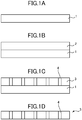
- Fig. 1A to Fig. 1D are cross-sectional views schematically showing a method of manufacturing a porous nickel thin film according to the embodiment.
- a conductive substrate 1 is prepared.
- a nickel plated film 2 is formed on the conductive substrate 1.
- the nickel plated film 2 is formed using a nickel electroplating bath which contains a nickel salt and a surfactant. Since the nickel electroplating bath contains a surfactant here, the nickel plated film 2 formed has the surfactant taken therein.
- the nickel plated film 2 is heat-treated. Heat treatment burns and removes the surfactant taken in the nickel plated film 2. Then, pores 4 penetrating in the thickness direction are formed in the nickel plated film 2, and a porous nickel thin film 3 is obtained as a result.
- the nickel thin film 3 is peeled off the conductive substrate 1 as shown in Fig. 1D .
- a substrate with low adhesion to the nickel thin film 3 as the conductive substrate 1.
- a substrate includes a metal substrate such as for example a Ti substrate, a Cu substrate, and an SUS substrate, and glass and resin material which are given electrical conductivity. Note that heat treatment for removing the surfactant may be carried out after the nickel thin film 3 is peeled off the conductive substrate 1.
- the nickel thin film 3 does not necessarily have to be peeled off the conductive substrate 1.
- the nickel thin film 3 may be peeled off the conductive substrate 1.
- the porous nickel thin film 3 which is excellent in flexibility.
- the porous nickel thin film 3 which has a flexibility value of 15.0 N/mm or less, preferably 10.0 N/mm or less, more preferably 1.0 to 10.0 N/mm, and still more preferably 3.0 to 8.0 N/mm.
- the porous nickel thin film 3 having such flexibility values is a novel metal film obtainable by the manufacturing method of the present invention, excellent in flexibility, and useful in various applications.
- the "flexibility value" in the present specification can be determined by the method of evaluating the porous nickel thin film and the method explained in Examples to be described later.
- the porous nickel thin film 3 obtained in the embodiment is also excellent in thermal resistance. There is a case where the shape of a nickel thin film manufactured by e.g. rolling is not maintained because oxidation proceeds during high temperature heating. In contrast, the shape of the porous nickel thin film 3 obtained in the embodiment is maintained even during high temperature heating.
- the thickness of the nickel thin film 3 obtained in the embodiment is preferably 0.1 ⁇ m to 100 ⁇ m, more preferably 1 ⁇ m to 10 ⁇ m, and still more preferably 2 ⁇ m to 8 ⁇ m. Too large a thickness makes it difficult to form pores, raises the processing difficulty, and leads to an increase in the manufacturing cost. Conversely, too small a thickness leads to insufficient strength.
- the use of the nickel thin film 3 obtained in the embodiment is not particularly limited.
- the nickel thin film 3 is useful as: a high performance catalytic film; a high performance filter; an undercoat for coating, painting, and plating; a functional coat and a thermal radiation coat used at high temperatures; and a surface coat for a slidable component.
- the nickel thin film 3 is used as-is, or catalytic particles such as Pt and Pd particles are scattered and held in the pores of the nickel thin film 3.
- the penetration pores formed in the nickel thin film 3 are used as fluid passages.
- flexibility is important in terms of the life of the coat.
- the nickel thin film 3 of the embodiment is preferable because it can satisfy such a requirement.
- the nickel thin film 3 obtained in the embodiment is useful as a functional coat and a thermal radiation coat which are required to have thermal resistance because it is not broken even under a high temperature atmosphere.
- the nickel thin film 3 of the embodiment has a large surface area because it is provided with pores. For this reason, if the nickel thin film 3 is used as an undercoat for e.g. coating, painting, and plating, it is possible to increase physical adhesion between the nickel thin film 3 and a film formed thereon.
- the nickel thin film 3 of the embodiment is used as a surface coat of a slidable component, it is possible to enhance lubricant retainability and to extend the life of the slidable component thanks to the pores provided.
- the plating bath used in the embodiment is an aqueous solution containing a nickel salt and a surfactant.
- the nickel salt acts as a supply source of nickel ions.
- the nickel salt is not particularly limited, it is preferable to use a compound selected from the group consisting of nickel sulfamate, nickel chloride, nickel sulfate, and nickel citrate.
- the nickel salt preferably contains nickel sulfamate. A coating with a low internal stress and high flexibility is obtained by use of nickel sulfamate.
- the concentration of the nickel salt in the plating bath is preferably 100 g/L to 800 g/L. Too high a concentration of the nickel salt reduces the saturation concentration of the surfactant, makes it difficult to form pores, and increases the possibility of losing flexibility. Too low a concentration of the nickel salt reduces the limiting current density due to insufficient concentration of the metal salt, increases the possibility of producing hydrogen gas during the formation of the coating, and increases the risk of cracks caused by the occlusion of hydrogen into the conductive substrate 1 being the undercoat. Moreover, too low a concentration is likely to produce a rough Ni plated coating with numerous pinholes.
- an ionic surfactant as the surfactant contained in the plating bath. It is preferable to use an anionic surfactant as the ionic surfactant.
- anionic surfactant examples include a compound selected from the group consisting of a polyoxyalkylene alkyl ether sulfate, a polyoxyalkylene alkyl ether carboxylate, a polyoxyalkylene alkyl ether sulfosuccinate, a polyoxyalkylene alkyl ether phosphate, a polyoxyalkylene alkyl ether acetate, an alkylbenzene sulfonate, a higher alcohol sulfate, a polyoxyalkylene styrenated phenyl ether sulfate, an alkyl diphenyl ether sulfonate, an alpha olefin sulfonate, a dialkyl sulfosuccinate, an alkane sulfonate, a secondary alkane sulfonate, an alkyl naphthalene sulfonate, a formaldehyde condens
- a more preferable compound is one selected from the group consisting of the polyoxyalkylene alkyl ether sulfate, the polyoxyalkylene alkyl ether carboxylate, the polyoxyalkylene alkyl ether acetate, and the alkylbenzene sulfonate among the above.
- each of the polyoxyalkylene alkyl ether sulfate and the polyoxyalkylene alkyl ether carboxylate is preferably an ethylene oxide-containing compound expressed by Formula 1 below: (Formula 1) : R1-O-(CH 2 CH 2 O) n -X
- R1 represents an alkyl group, preferably an alkyl group having 10 to 16 carbon atoms, and more preferably an alkyl group having 12 to 14 carbon atoms.
- the letter X indicates a sulfate or a carboxylate.
- the letter n ranges from 1 to 20, preferably from 2 to 12.
- alkylbenzene sulfonate is preferably a compound having 8 to 16 carbon atoms in the alkyl group, more preferably a dodecylbenzene sulfonate.
- the counter ions used as the salt of the anionic surfactant include alkali metal salts such as a sodium salt and a potassium salt, alkali earth metal salts, ammonium salts, and alkanolamine salts. Among these, the alkali metal salts are preferable, and the sodium salt is more preferable.
- the concentration of the surfactant in the plating bath is preferably 0.1 mL/L to 100 mL/L, more preferably 1 mL/L to 50 mL/L, and still more preferably 5 mL/L to 30 mL/L. Too high a concentration of the surfactant makes it difficult to obtain a fine coating because plate deposition is hindered. On the other hand, too low a concentration makes it difficult to form pores, which makes it hard to obtain desired flexibility.
- additives may be added to the plating bath such as a pH adjuster, a pH buffer, and a stress releaser.
- a pH adjuster e.g., Sulfuric acid, sulfamic acid, nickel hydroxide, etc.
- Saccharin etc. are used as the stress releaser, for example.
- the pH of the plating bath is preferably 2.0 to 4.5. Too high a pH reduces the limiting current density, increases the possibility of producing hydrogen gas, and increases the risk of occlusion of hydrogen into the conductive substrate 1. Moreover, the Ni coating is likely to become hard and brittle. On the other hand, too low a pH is likely to promote decomposition of the plating bath components.
- the bath temperature of the plating bath during plating is preferably 40°C to 65°C. Too high a bath temperature is likely to promote the decomposition of the bath components. On the other hand, too low a bath temperature increases the possibility of surfactant precipitation. Moreover, extraneous deposition of nickel is likely to take place.
- electroplating is possible using a direct current electrolysis, it is more preferable to carry out pulse electroplating.
- pulse electroplating at the early stages of deposition, it is possible to cause the surfactant to scatter and be adsorbed to the conductive substrate 1 being the undercoat, and to promote eutectoid between the surfactant and nickel during plating.
- the average current density is preferably 1 A/dm 2 to 20 A/dm 2 . Too high an average current density may lead to excessive production of hydrogen, affecting the conductive substrate 1 being the undercoat. Furthermore, extraneous deposition of nickel might take place. On the other hand, too low an average current density makes it difficult to form pores, which makes it hard to obtain desired flexibility. Also, productivity is reduced.
- the pulse current density is preferably 2 A/dm 2 to 20 A/dm 2 . Too high a pulse current density may cause excessive production of hydrogen, affecting the conductive substrate 1 being the undercoat. Furthermore, extraneous deposition of nickel might take place. On the other hand, too low a pulse current density makes it difficult to form pores, reducing productivity.
- the ratio of the pulse applying time ton to the pulse pause time toff is more preferably 0.1 to 10. Too large a ratio (ton/toff) makes it difficult to form pores, which makes it hard to obtain desired flexibility. Conversely, too small a ratio also makes it difficult to form pores, which makes it hard to obtain desired flexibility.
- the pulse frequency is preferably 0.1 to 1000 (Hz) . Too large a pulse frequency makes it difficult to form pores, which makes it hard to obtain desired flexibility. Conversely, too small a pulse frequency also makes it difficult to form pores, which makes it hard to obtain desired flexibility.
- Heat treatment is carried out under the conditions where the surfactant is burnt and removed in, for example, the atmosphere, a reducing atmosphere such as hydrogen, or an inactive atmosphere such as nitrogen or argon.
- the heat treatment temperature is 350°C to 900°C, for example.
- the heating time is 10 minutes to 120 minutes, for example. Too high a heating temperature is likely to increase the cost of mass production processing. Worse, the possibility of losing flexibility is increased because an interdiffusion layer is likely to be formed between the conductive substrate 1 being the undercoat and the nickel plated film 2. On the other hand, too low a heat treatment temperature makes it difficult for porosification to occur, which makes it impossible to obtain desired flexibility. In addition, too long a heating time also increases the possibility of forming an interdiffusion layer. Conversely, too short a heating time makes it difficult for porosification to occur, increasing the possibility of losing flexibility.
- the nickel thin film 3 which is manufactured by the method according to the embodiment has a property excellent in flexibility.
- the "flexibility value” is a value determined using an evaluation method to be described below.
- Fig. 2 is a view of an external appearance of an evaluation apparatus 10 used in the evaluation method for the flexibility value.
- Fig. 3 is a schematic view showing the evaluation apparatus 10.
- the evaluation apparatus 10 includes a body part 16, a stage 11, a pushing jig support 13, a measurement apparatus 18, a pushing jig 14, a subject supporting jig 12, and a drive mechanism 15. Note that the pushing jig 14 and the subject supporting jig 12 are detachable and illustrated only in Fig. 3 , not in Fig. 2 .
- the stage 11 is provided to support the subject supporting jig 12, and is supported by the body part 16.
- the subject supporting jig 12 is provided to support the nickel thin film 3 to be tested (see Fig. 3 ).
- the subject supporting jig 12 is detachably attached to the stage 11.
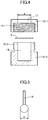
- Fig. 4 is a cross-sectional view schematically showing the subject supporting jig 12.
- the subject supporting jig 12 includes a pair of clamping members (12-1 and 12-2) .
- One clamping member 12-1 has an opening 17 provided therein.
- the other clamping member 12-2 has a hollow portion 16 provided at the position corresponding to the opening 17.
- Each of the opening 17 and the hollow portion 16 has the shape of a circle with a predetermined diameter of a. Note that the clamping member 12-2 may be provided with an opening instead of the hollow portion 16.
- each clamping member (12-1 and 12-2) is provided with a screw thread (19-1 and 19-2), and it is thus possible to threadly engage the clamping member 12-1 with the clamping member 12-2 while clamping the nickel thin film 3.
- the center portion of the nickel thin film 3, that is, the region corresponding to the opening 17 is not in contact with the subject supporting jig 12. That is to say, the subject supporting jig 5 is configured to support the entire periphery of the nickel thin film 3, and an unsupported region with a closed shape corresponding to the opening 17 is formed in the center portion of the nickel thin film 3.
- the pushing jig support 13 (see Fig. 2 and Fig. 3 ) is provided to support the pushing jig 14.
- the pushing jig support 13 is attached to the body part 16 so as to be movable in a direction perpendicular to the nickel thin film 3.
- the drive mechanism 15 is attached to the body part 16 and has a function of causing the pushing jig support 13 to travel.
- the drive mechanism 15 is a motor, for example.
- the pushing jig 14 has the shape of a rod.
- the pushing jig 14 is supported above the nickel thin film 3 by the pushing jig support 13 so as to extend in a direction perpendicular to the nickel thin film 3.
- one end (lower end) of the pushing jig 14 is set so as to be positioned right above the center of the opening 17 provided in the clamping member 12-1.
- Fig. 5 is a schematic view showing an example of the pushing jig 14. As shown in Fig. 5 , one end of the pushing jig 14 preferably has a shape corresponding to a portion of a sphere with a predetermined diameter of b.
- the measurement apparatus 18 has a function of detecting the force applied to the pushing jig 14 and the displacement amount of the pushing jig 14.
- the measurement apparatus 18 includes a load cell 18-1 and an encoder 18-2.
- the load cell 18-1 is provided between the pushing jig support 13 and the pushing jig 14 and has a function of detecting the force applied to the pushing jig 14.
- the encoder 18-2 is connected to the drive mechanism 15 and is configured to detect the displacement amount of the pushing jig support 13, that is, a displacement amount of the pushing jig 14.
- the drive mechanism 15 moves the pushing jig support 13 downwards (toward the subject supporting jig 12). This pushes one end of the pushing jig 14 aligned with the center of the opening 17 perpendicularly into the nickel thin film 3, as shown in Fig. 6 .
- the pushing jig 14 is pushed in until the nickel thin film 3 is torn.
- the measurement apparatus 18 measures the force applied to the pushing jig 14 and the displacement amount of the pushing jig 14.
- the measurement results are stored in e.g. a computer (not shown) as data indicating the relationship between the force applied to the pushing jig 14 and the displacement amount of the pushing jig 14.
- the flexibility value of the nickel thin film 3 is determined based on the obtained data.
- the "flexibility value” is a value expressed by a value (N/mm) which is the force (N) applied to the pushing jig divided by the displacement amount (mm) of the pushing jig. The smaller this value, the more flexible the nickel thin film 3 is.
- the flexibility value can be calculated by creating a graph with the horizontal axis representing the displacement amount and the vertical axis representing the force (test force) applied to the pushing jig 14, and by determining the gradient within a range where the linearity is good (for example, a region where the correlation coefficient R 2 determined by linear approximation is larger than 0.9).
- the evaluation method described above makes it possible to properly evaluate the flexibility of the nickel thin film 3 with a thickness of 0.1 to 100 ⁇ m.
- the diameter a of the opening 17 provided in the clamping member 12-1 is preferably 9 mm to 14 mm, more preferably 10 mm to 13 mm, and still more preferably 11 mm to 12 mm. Too small a diameter a makes it impossible to obtain a sufficient displacement amount for the test force, while a too large a diameter requires a large sample area.
- the shape of one end of the pushing jig 14 is preferably a shape corresponding to a portion of a sphere with a diameter of b, as already described.
- the pushing jig 14 touches the test piece at the vertexes. This increases the risk of tearing the test piece before the completion of the test because the test force concentrates at the vertexes. As a result, it becomes difficult to create a region with a high-linearity relationship in the test force-displacement amount graph.
- the shape of one end of the pushing jig 14 is a flat-plate shape such as a flat plate circle, the test piece deforms to make an acute angle at an edge of this flat-plate shape. For this reason, it becomes difficult to obtain a high-linearity relationship.
- the shape of one end of the pushing jig 14 has a shape corresponding to a portion of a sphere, one obtains an effect of pushing the test piece with a surface.
- the pushing jig 14 is being pushed in, the test piece is smoothly stretched while making an obtuse angle. This helps to obtain a higher-linearity relationship.
- the diameter b is preferably 5 mm to 10 mm, more preferably 6 mm to 9 mm, and still more preferably 7 mm to 8 mm. Too small a diameter b means that the test piece is pressed at a point, increasing the risk that the test piece is easily torn. On the other hand, too large a diameter b means that the subject supporting jig 12 also needs to be large, increasing the necessary sample area.
- the ratio of the diameter b to the diameter a of the opening 17 is preferably 0.3 to 0.9, more preferably 0.4 to 0.8, and still more preferably 0.5 to 0.7.
- the ratio of the diameter b to the diameter a within such ranges helps to obtain a high-linearity relationship.
- the push rate of the pushing jig 14 is preferably 0.1 mm/min to 10.0 mm/min, more preferably 0.5 mm/min to 5.0 mm/min, and still more preferably 1.0 mm/min to 2.0 mm/min. Too low a push rate requires a long time test. On the other hand, too high a push rate increases the risk of breaking the test piece, and the test piece is likely to be broken before a region with a high linearity is sufficiently obtained.
- An SUS substrate was prepared as the conductive substrate 1 being the undercoat.
- the nickel plated film 2 was formed on this conductive substrate 1 by electroplating.
- the aqueous solution used as the electroplating bath contained 600 g/L of nickel sulfamate, 10 g/L of nickel chloride, 40 g/L of boric acid, and 10 ml/L of anionic surfactant (sodium dodecylbenzenesulfonate).
- the pH of the plating bath was 3.5, and the bath temperature was 60°C.
- the electroplating was carried out by pulse plating. Pulse plating was carried out under the conditions that the average current density was 5.9 A/dm 2 and the ratio (ton/toff) was 1.4.
- the nickel plated film 2 was peeled off the conductive substrate 1. Furthermore, heat treatment was carried out at 500°C on the nickel plated film 2 for 60 minutes in the atmosphere, and the nickel thin film 3 according to Example 1 was obtained. The thickness of the obtained nickel thin film 3 was 5 ⁇ m.
- the nickel thin film 3 according to Example 2 was obtained using the same method as in Example 1, but the heat treatment time was 120 minutes.
- the nickel thin film 3 according to Comparative Example 1 was obtained using the same method as in Example 1, but the heat treatment was not carried out.
- the nickel thin film 3 according to Comparative Example 2 was obtained using the same method as in Example 1, but the heat treatment was not carried out.
- the solution used as the electroplating bath had 350 g/L of nickel sulfate, 60 g/L of nickel chloride, 30 g/L of trisodium citrate dissolved therein (no surfactant contained).
- the pH of the plating bath was 4.6 and the bath temperature was 60°C.
- a nickel film with a thickness of 10 ⁇ m manufactured by rolling was prepared as the nickel thin film according to Comparative Example 3.
- a Cu film with a thickness of 10 ⁇ m manufactured by rolling was prepared as the metal film according to Comparative Example 4.
- each of the test pieces was cut to form a circle with a diameter of 20 mm. Then, the test piece was clamped and secured on the stage 11 by use of the pair of clamping members (12-1 and 12-2) which have the opening 17 and the hollow portion 16 both with a diameter of 12 mm. Further, a jig having on one end a shape corresponding to a portion of a sphere with a diameter of 7 mm was prepared as the pushing jig 14, and was attached to the pushing jig support 13. The pushing jig support 13 was moved toward the pair of clamping members 12 at a rate of 1 mm/min. Thereby, one end of the pushing jig 14 aligned with the center of the opening 17 was caused to touch the test piece. Moreover, the pushing jig 14 was pushed in until the test piece was torn, and the relationship between the displacement amount of the pushing jig 14 and the test force (force applied to the pushing jig 14) was measured with the measurement apparatus 18.
- Fig. 7 is a graph showing measurement results.
- the correspondence relationship between the curves and Examples 1 to 2 and Comparative Examples 1 to 5 is as follows:
- a portion of sudden decrease in the test force corresponds to a point at which the test piece is torn (hereinafter referred to as a breaking point) .
- a breaking point a point at which the test piece is torn.
- the nickel thin films 3 according to Examples 1 and 2 have larger displacement amounts until the test piece is broken compared to the nickel thin films and the metal films according to Comparative Examples 1 to 5. Furthermore, as compared to Comparative Examples 1 to 5, Examples 1 and 2 have a larger area of the region surrounded by the origin, the breaking point, and the point on the X-axis corresponding to the breaking point, i.e. a larger amount of work with respect to elongation. This indicates that Examples 1 and 2 have higher elongation properties, higher flexibility, and higher mechanical strengths compared to Comparative Examples 1 to 5.
- Fig. 8 is a graph showing results of calculating "flexibility values.” Note that the "flexibility values" were calculated by determining a range where the linearity is good (correlation coefficient R 2 > 0.9 in linear approximation) in the graph shown in Fig. 7 and by determining the gradient. As shown in Fig. 8 , Examples 1 and 2 have smaller “flexibility values” compared to Comparative Examples 1 and 2. To be more precise, it is understood that a nickel thin film 3 with a high elongation property and high flexibility can be obtained by carrying out electroplating with a plating bath containing a surfactant, and by removing the surfactant through heat treatment. Moreover, it is understood that the nickel thin films 3 of Examples 1 and 2 have smaller flexibility values compared to the metal films of Comparative Example 3 and 4, and have higher elongation properties and higher flexibility compared to the nickel film and the Cu film obtained by rolling.
Landscapes
- Chemical & Material Sciences (AREA)
- Engineering & Computer Science (AREA)
- Chemical Kinetics & Catalysis (AREA)
- Electrochemistry (AREA)
- Materials Engineering (AREA)
- Metallurgy (AREA)
- Organic Chemistry (AREA)
- Electroplating Methods And Accessories (AREA)
- Electroplating And Plating Baths Therefor (AREA)
Applications Claiming Priority (2)
| Application Number | Priority Date | Filing Date | Title |
|---|---|---|---|
| JP2015218685A JP6319771B2 (ja) | 2015-11-06 | 2015-11-06 | 多孔質ニッケル薄膜及びその製造方法 |
| PCT/JP2016/082608 WO2017078069A1 (fr) | 2015-11-06 | 2016-11-02 | Film mince de nickel poreux et son procédé de fabrication |
Publications (2)
| Publication Number | Publication Date |
|---|---|
| EP3296432A1 true EP3296432A1 (fr) | 2018-03-21 |
| EP3296432A4 EP3296432A4 (fr) | 2018-12-19 |
Family
ID=58662202
Family Applications (1)
| Application Number | Title | Priority Date | Filing Date |
|---|---|---|---|
| EP16862129.0A Withdrawn EP3296432A4 (fr) | 2015-11-06 | 2016-11-02 | Film mince de nickel poreux et son procédé de fabrication |
Country Status (6)
| Country | Link |
|---|---|
| US (1) | US20180230615A1 (fr) |
| EP (1) | EP3296432A4 (fr) |
| JP (1) | JP6319771B2 (fr) |
| CN (1) | CN107614756A (fr) |
| TW (1) | TWI617672B (fr) |
| WO (1) | WO2017078069A1 (fr) |
Families Citing this family (9)
| Publication number | Priority date | Publication date | Assignee | Title |
|---|---|---|---|---|
| JP6503149B1 (ja) | 2017-07-06 | 2019-04-17 | 浜松ホトニクス株式会社 | 光学デバイス及びその製造方法 |
| CN110799884B (zh) | 2017-07-06 | 2022-03-01 | 浜松光子学株式会社 | 光学装置 |
| TWI784023B (zh) | 2017-07-06 | 2022-11-21 | 日商濱松赫德尼古斯股份有限公司 | 光學裝置 |
| WO2019009398A1 (fr) * | 2017-07-06 | 2019-01-10 | 浜松ホトニクス株式会社 | Dispositif optique |
| JP7112876B2 (ja) | 2017-07-06 | 2022-08-04 | 浜松ホトニクス株式会社 | 光学デバイス |
| TWI822686B (zh) | 2017-07-06 | 2023-11-21 | 日商濱松赫德尼古斯股份有限公司 | 光學裝置 |
| JP6514804B1 (ja) | 2017-07-06 | 2019-05-15 | 浜松ホトニクス株式会社 | 光学デバイス |
| WO2019009397A1 (fr) | 2017-07-06 | 2019-01-10 | 浜松ホトニクス株式会社 | Dispositif optique |
| CN115657297A (zh) | 2017-11-15 | 2023-01-31 | 浜松光子学株式会社 | 光学器件的制造方法 |
Family Cites Families (16)
| Publication number | Priority date | Publication date | Assignee | Title |
|---|---|---|---|---|
| JP2716322B2 (ja) * | 1992-08-24 | 1998-02-18 | 株式会社 イケックス工業 | メッキ製品の製造方法 |
| JP2001085015A (ja) * | 1999-09-17 | 2001-03-30 | Sumitomo Metal Steel Products Inc | アルカリ蓄電池負極用多孔ニッケル箔およびその製造方法 |
| AU2001213092A1 (en) * | 2000-11-13 | 2002-05-21 | Matsushita Electric Industrial Co., Ltd. | Porous nickel foil for alkaline battery cathode, production method therefor and production device therefor |
| JP2003293188A (ja) * | 2002-04-09 | 2003-10-15 | Sumitomo Metal Mining Co Ltd | ニッケルめっき皮膜 |
| CN101298686B (zh) * | 2007-04-30 | 2010-09-29 | 比亚迪股份有限公司 | 一种泡沫金属的制备方法 |
| JP5366076B2 (ja) * | 2008-11-21 | 2013-12-11 | 奥野製薬工業株式会社 | 多孔質めっき皮膜形成用添加剤を含有する多孔質めっき皮膜用電気めっき浴 |
| TWI429789B (zh) * | 2010-03-11 | 2014-03-11 | Omron Tateisi Electronics Co | 接觸件製造用組成物及使用其之接觸件以及連接器及製造接觸件製造用組成物之方法 |
| JP5487487B2 (ja) * | 2010-08-20 | 2014-05-07 | 富山住友電工株式会社 | 金属多孔体及びその製造方法 |
| JP5635382B2 (ja) * | 2010-12-08 | 2014-12-03 | 住友電気工業株式会社 | 高耐食性を有する金属多孔体の製造方法 |
| JP2013014819A (ja) * | 2011-07-06 | 2013-01-24 | Murata Mfg Co Ltd | 多孔質金属膜、電極、集電体、電気化学センサ、蓄電デバイス及び摺動部材並びに多孔質金属膜の製造方法 |
| JP6212869B2 (ja) * | 2012-02-06 | 2017-10-18 | 三菱マテリアル株式会社 | 酸化物スパッタリングターゲット |
| JP6047711B2 (ja) * | 2012-02-08 | 2016-12-21 | 石原ケミカル株式会社 | 無電解ニッケル及びニッケル合金メッキ方法、並びに当該メッキ用の前処理液 |
| CN103243357B (zh) * | 2013-05-13 | 2015-09-23 | 重庆大学 | 三维多孔镍薄膜的制备方法 |
| CN107849724A (zh) * | 2014-10-29 | 2018-03-27 | 林科闯 | 多孔材料及系统及其制造方法 |
| JP6056023B2 (ja) * | 2014-11-05 | 2017-01-11 | 株式会社山王 | 金属複合水素透過膜とその製造方法 |
| JP6014920B1 (ja) * | 2015-08-19 | 2016-10-26 | 株式会社山王 | 金属複合水素透過膜とその製造方法 |
-
2015
- 2015-11-06 JP JP2015218685A patent/JP6319771B2/ja active Active
-
2016
- 2016-11-02 CN CN201680029173.3A patent/CN107614756A/zh active Pending
- 2016-11-02 WO PCT/JP2016/082608 patent/WO2017078069A1/fr not_active Ceased
- 2016-11-02 US US15/575,236 patent/US20180230615A1/en not_active Abandoned
- 2016-11-02 EP EP16862129.0A patent/EP3296432A4/fr not_active Withdrawn
- 2016-11-04 TW TW105135885A patent/TWI617672B/zh active
Also Published As
| Publication number | Publication date |
|---|---|
| TWI617672B (zh) | 2018-03-11 |
| EP3296432A4 (fr) | 2018-12-19 |
| US20180230615A1 (en) | 2018-08-16 |
| WO2017078069A1 (fr) | 2017-05-11 |
| JP2017088940A (ja) | 2017-05-25 |
| JP6319771B2 (ja) | 2018-05-09 |
| TW201718896A (zh) | 2017-06-01 |
| CN107614756A (zh) | 2018-01-19 |
Similar Documents
| Publication | Publication Date | Title |
|---|---|---|
| EP3296432A1 (fr) | Film mince de nickel poreux et son procédé de fabrication | |
| TWI510672B (zh) | 無電金屬化方法 | |
| TW201316849A (zh) | 抗高溫之銀塗覆基板 | |
| KR20130006658A (ko) | 코팅된 물품 및 방법 | |
| JP7542094B2 (ja) | 銀めっき材およびその製造方法 | |
| JP4494155B2 (ja) | 金めっき構造体およびこの金めっき構造体からなる燃料電池用セパレーター | |
| CN105349971A (zh) | 一种铝合金表面改性工艺 | |
| Zhu et al. | Electrochemical behaviors of the magnesium alloy substrates in various pretreatment solutions | |
| CN105408527B (zh) | 表面处理铝材及其制造方法 | |
| US20130177777A1 (en) | Coated article and method for making same | |
| Satpathy et al. | Multifaceted insights into Au coatings electrodeposited from a ChCl-EG based Deep Eutectic Solvent (DES): Unravelling the effect of surfactant polarity and current density on the morphology, mechanical properties, and anti-tarnishing efficacy | |
| JP6575968B2 (ja) | 表面処理アルミニウム材及びその製造方法、ならびに、当該表面処理アルミニウム材/樹脂層の接合体 | |
| CN103757675B (zh) | 一种afm硅针尖脉冲电镀纳米厚度致密金薄膜方法 | |
| US9783902B2 (en) | Method for producing plated article | |
| JP6352087B2 (ja) | 表面処理アルミニウム材及びその製造方法 | |
| Yae et al. | Electroless Metallization of Silicon Using Metal Nanoparticles as Catalysts and Binding-Points | |
| JP6029202B2 (ja) | アルミニウムまたはアルミニウム合金材への純鉄の電気めっき方法 | |
| Silkin et al. | Effect of bulk current density on tribological properties of Fe-W, Co-W and Ni-W coatings | |
| Sadowska-Mazur et al. | Electrodeposition and properties of tin-nickel/silicon carbide composite coatings | |
| CN101460664B (zh) | 次膦酸和/或膦酸在氧化还原法中的用途 | |
| Liu et al. | The effect of pulse reversal on morphology of cobalt hard gold | |
| CN114318342A (zh) | 一种去除钢板镀锌层的腐蚀溶液及显示镀锌钢板抑制层的方法 | |
| JP2013189667A (ja) | 無電解めっき方法及び金属被膜形成方法 | |
| JP6570168B2 (ja) | 表面処理アルミニウム材及びその製造方法 | |
| JP6084899B2 (ja) | 低熱膨張係数および高硬度を有する鉄−ニッケル合金用電気メッキ浴およびこれを用いた電気メッキ方法 |
Legal Events
| Date | Code | Title | Description |
|---|---|---|---|
| PUAI | Public reference made under article 153(3) epc to a published international application that has entered the european phase |
Free format text: ORIGINAL CODE: 0009012 |
|
| 17P | Request for examination filed |
Effective date: 20171214 |
|
| AK | Designated contracting states |
Kind code of ref document: A1 Designated state(s): AL AT BE BG CH CY CZ DE DK EE ES FI FR GB GR HR HU IE IS IT LI LT LU LV MC MK MT NL NO PL PT RO RS SE SI SK SM TR |
|
| AX | Request for extension of the european patent |
Extension state: BA ME |
|
| A4 | Supplementary search report drawn up and despatched |
Effective date: 20181119 |
|
| RIC1 | Information provided on ipc code assigned before grant |
Ipc: C25D 5/18 20060101ALI20181113BHEP Ipc: C25D 1/00 20060101ALI20181113BHEP Ipc: C25D 1/08 20060101AFI20181113BHEP Ipc: B01D 71/02 20060101ALI20181113BHEP Ipc: C25D 3/12 20060101ALI20181113BHEP Ipc: C25D 1/04 20060101ALI20181113BHEP |
|
| DAV | Request for validation of the european patent (deleted) | ||
| DAX | Request for extension of the european patent (deleted) | ||
| STAA | Information on the status of an ep patent application or granted ep patent |
Free format text: STATUS: THE APPLICATION IS DEEMED TO BE WITHDRAWN |
|
| 18D | Application deemed to be withdrawn |
Effective date: 20190618 |