EP3296725A2 - Procédé d'inspection de défauts et appareil faisant appel à une matrice de microlentilles - Google Patents
Procédé d'inspection de défauts et appareil faisant appel à une matrice de microlentilles Download PDFInfo
- Publication number
- EP3296725A2 EP3296725A2 EP17191253.8A EP17191253A EP3296725A2 EP 3296725 A2 EP3296725 A2 EP 3296725A2 EP 17191253 A EP17191253 A EP 17191253A EP 3296725 A2 EP3296725 A2 EP 3296725A2
- Authority
- EP
- European Patent Office
- Prior art keywords
- pixel
- light
- microlens array
- optical waveguide
- substrate
- Prior art date
- Legal status (The legal status is an assumption and is not a legal conclusion. Google has not performed a legal analysis and makes no representation as to the accuracy of the status listed.)
- Granted
Links
Images


Classifications
-
- G—PHYSICS
- G01—MEASURING; TESTING
- G01N—INVESTIGATING OR ANALYSING MATERIALS BY DETERMINING THEIR CHEMICAL OR PHYSICAL PROPERTIES
- G01N21/00—Investigating or analysing materials by the use of optical means, i.e. using sub-millimetre waves, infrared, visible or ultraviolet light
- G01N21/84—Systems specially adapted for particular applications
- G01N21/88—Investigating the presence of flaws or contamination
- G01N21/95—Investigating the presence of flaws or contamination characterised by the material or shape of the object to be examined
- G01N21/9501—Semiconductor wafers
-
- G—PHYSICS
- G06—COMPUTING OR CALCULATING; COUNTING
- G06T—IMAGE DATA PROCESSING OR GENERATION, IN GENERAL
- G06T5/00—Image enhancement or restoration
- G06T5/80—Geometric correction
-
- G—PHYSICS
- G01—MEASURING; TESTING
- G01N—INVESTIGATING OR ANALYSING MATERIALS BY DETERMINING THEIR CHEMICAL OR PHYSICAL PROPERTIES
- G01N21/00—Investigating or analysing materials by the use of optical means, i.e. using sub-millimetre waves, infrared, visible or ultraviolet light
- G01N21/84—Systems specially adapted for particular applications
- G01N21/88—Investigating the presence of flaws or contamination
- G01N21/8806—Specially adapted optical and illumination features
-
- G—PHYSICS
- G01—MEASURING; TESTING
- G01N—INVESTIGATING OR ANALYSING MATERIALS BY DETERMINING THEIR CHEMICAL OR PHYSICAL PROPERTIES
- G01N21/00—Investigating or analysing materials by the use of optical means, i.e. using sub-millimetre waves, infrared, visible or ultraviolet light
- G01N21/84—Systems specially adapted for particular applications
- G01N21/88—Investigating the presence of flaws or contamination
- G01N21/95—Investigating the presence of flaws or contamination characterised by the material or shape of the object to be examined
- G01N21/956—Inspecting patterns on the surface of objects
-
- G—PHYSICS
- G02—OPTICS
- G02B—OPTICAL ELEMENTS, SYSTEMS OR APPARATUS
- G02B3/00—Simple or compound lenses
- G02B3/0006—Arrays
- G02B3/0037—Arrays characterized by the distribution or form of lenses
-
- G—PHYSICS
- G06—COMPUTING OR CALCULATING; COUNTING
- G06T—IMAGE DATA PROCESSING OR GENERATION, IN GENERAL
- G06T7/00—Image analysis
- G06T7/0002—Inspection of images, e.g. flaw detection
-
- G—PHYSICS
- G06—COMPUTING OR CALCULATING; COUNTING
- G06T—IMAGE DATA PROCESSING OR GENERATION, IN GENERAL
- G06T7/00—Image analysis
- G06T7/0002—Inspection of images, e.g. flaw detection
- G06T7/0004—Industrial image inspection
-
- G—PHYSICS
- G06—COMPUTING OR CALCULATING; COUNTING
- G06T—IMAGE DATA PROCESSING OR GENERATION, IN GENERAL
- G06T7/00—Image analysis
- G06T7/0002—Inspection of images, e.g. flaw detection
- G06T7/0004—Industrial image inspection
- G06T7/0008—Industrial image inspection checking presence/absence
-
- G—PHYSICS
- G01—MEASURING; TESTING
- G01N—INVESTIGATING OR ANALYSING MATERIALS BY DETERMINING THEIR CHEMICAL OR PHYSICAL PROPERTIES
- G01N2201/00—Features of devices classified in G01N21/00
- G01N2201/06—Illumination; Optics
- G01N2201/063—Illuminating optical parts
- G01N2201/0638—Refractive parts
-
- G—PHYSICS
- G06—COMPUTING OR CALCULATING; COUNTING
- G06T—IMAGE DATA PROCESSING OR GENERATION, IN GENERAL
- G06T2207/00—Indexing scheme for image analysis or image enhancement
- G06T2207/10—Image acquisition modality
- G06T2207/10052—Images from lightfield camera
-
- G—PHYSICS
- G06—COMPUTING OR CALCULATING; COUNTING
- G06T—IMAGE DATA PROCESSING OR GENERATION, IN GENERAL
- G06T2207/00—Indexing scheme for image analysis or image enhancement
- G06T2207/30—Subject of image; Context of image processing
- G06T2207/30108—Industrial image inspection
- G06T2207/30121—CRT, LCD or plasma display
-
- G—PHYSICS
- G06—COMPUTING OR CALCULATING; COUNTING
- G06T—IMAGE DATA PROCESSING OR GENERATION, IN GENERAL
- G06T2207/00—Indexing scheme for image analysis or image enhancement
- G06T2207/30—Subject of image; Context of image processing
- G06T2207/30108—Industrial image inspection
- G06T2207/30148—Semiconductor; IC; Wafer
-
- H—ELECTRICITY
- H10—SEMICONDUCTOR DEVICES; ELECTRIC SOLID-STATE DEVICES NOT OTHERWISE PROVIDED FOR
- H10P—GENERIC PROCESSES OR APPARATUS FOR THE MANUFACTURE OR TREATMENT OF DEVICES COVERED BY CLASS H10
- H10P74/00—Testing or measuring during manufacture or treatment of wafers, substrates or devices
- H10P74/20—Testing or measuring during manufacture or treatment of wafers, substrates or devices characterised by the properties tested or measured, e.g. structural or electrical properties
- H10P74/203—Structural properties, e.g. testing or measuring thicknesses, line widths, warpage, bond strengths or physical defects
Definitions
- the present invention relates to semiconductor technology. More particularly, embodiments of the present invention relate to a substrate surface defect detection apparatus and method, an image distortion correction method and apparatus, and a system including a substrate surface defect detection apparatus and an image distortion correction apparatus.
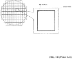
- FIG. 1A is a perspective view of a conventional substrate surface defect detection system 102.
- FIG. 1B is a plan view of a substrate 101 shown in FIG. 1A .
- the surface defects of a substrate 101 need to be detected using a sophisticated and complex optical system 102.
- FIG. 1B schematically shows the exposure area of substrate 101 and the effective field of view of substrate surface defect detection system 102.
- the effective field of view of substrate surface defect detection system 102 is typically about 30 ⁇ m x 30 ⁇ m. If system 102 is used to detect surface defects of substrate 101 having a typical exposure area of 26 mm x 33 mm, about one million operations must be performed to complete the surface defects detection (e.g., each shot only takes a field of view picture).
- aspects of the present invention provide an image distortion correction method and an image distortion correction device that are capable of correcting distortion of an image output from a substrate surface defect detection device.
- a further aspect of the present invention provides substrate surface defect detection and image correction system.
- Still a further aspect of the present invention provides a device and method for efficiently detecting substrate surface defects that can reduce the cost of defect detection.
- a substrate surface defect detection device includes an optical waveguide for receiving first light and directing the received first light to a surface of a to be tested substrate, the optical waveguide having a first surface facing toward the substrate and a second surface facing away from the substrate; at least one microlens array disposed on the second surface of the optical waveguide, the at least one microlens array comprising a plurality of microlenses arranged in an array for receiving second light from the surface of the to be tested substrate and converging the received second light to converged light; and an imaging component for receiving the converged light from the at least one microlens array for imaging.
- the imaging component includes a plurality of imaging units, each of the imaging units comprising a plurality of pixels, each of the imaging units being associated with one of the microlenses to receive a portion of the converged light.
- the at least one microlens array includes a first microlens array and a second microlens array stacked over each other.
- Each of the first and second microlens arrays has a plurality of microlenses, each of the microlenses of the first microlens array has an optical axis aligned to an optical axis of one corresponding microlens of the second microlens array.
- the substrate surface defect detection device further includes a plurality of light confinement members disposed between a corresponding imaging unit and a corresponding microlens and configured to enable light from the corresponding microlens to reflect a specific field of view to pass therethrough and into the corresponding imaging unit.
- the light confinement members each comprise a light blocking plate.
- the light confinement members each include a cylindrical optical member having a light receiving surface and a light exit surface.
- the at least one microlens array further comprises a support member disposed at an edge of the microlenses.
- the at least one microlens array includes a first microlens array and a second microlens array stacked over each other, and the support member of the first microlens array and the support member of the second microlens array are aligned with each other.
- the support member is formed of a same material as a material of the microlenses and includes a barrier layer on a lower surface for blocking light from entering the support member.
- the barrier layer includes a metal plating layer.
- the support member is formed of a same material as a material of the microlenses, and a surface portion of the optical waveguide below the support member includes a barrier layer for blocking light from entering the support member.
- each of the microlenses includes a plano-convex lens.
- the coordinates of a point on an aspheric surface of the plano-convex lens in a z-direction parallel to an optical axis has a second order function term and a fourth order function term of a distance from a corresponding plane projection point perpendicular to the optical axis.
- r is a distance from a point of the aspheric surface perpendicular to the optical axis
- Z is the coordinate of the point on the aspheric surface of the lens in the Z-direction
- R is the radius of curvature from the optical axis to the lens surface
- K is a conic constant
- ⁇ 1 is an aspheric surface coefficient of the second order function term
- ⁇ 2 is an aspheric surface coefficient of the fourth order function term.
- the optical waveguide includes a first incident surface and a second incident surface disposed on opposite sides of the optical waveguide; the first light includes third light and fourth light, the third light entering the optical waveguide from the first incident surface and the fourth light entering the optical waveguide from the second incident surface.
- the first incident surface and the second incident surface are inclined with respect to the first surface of the optical waveguide.
- the substrate surface defect detection device further includes a laser light source for generating a laser beam; a semitransparent mirror disposed at an angle relative to an optical axis of the laser beam for splitting the laser beam into first partial light and second partial light; and a first light generating member for generating a first beam and including a first beam expander for expanding the first partial light in a first dimension to generate a first laser beam, a first lens for converging the first laser beam in a second dimension different from the first dimension to generate a converged first laser beam, and a first mirror for reflecting the converged first laser beam as the third light entering the optical waveguide from the first incident surface.
- a laser light source for generating a laser beam
- a semitransparent mirror disposed at an angle relative to an optical axis of the laser beam for splitting the laser beam into first partial light and second partial light
- a first light generating member for generating a first beam and including a first beam expander for expanding the first partial light in a first dimension to generate a first laser beam
- the substrate surface defect detection device further includes a second mirror for reflecting the second partial light, and a second light generating member for generating a second beam that includes a second beam expander for expanding the second partial light in the first dimension to generate a second laser beam, a second lens for converging the second laser beam in the second dimension to generate a converged second laser beam, and a third mirror for reflecting the converged second laser beam as the fourth light entering the optical waveguide from the second incident surface.
- a second mirror for reflecting the second partial light
- a second light generating member for generating a second beam that includes a second beam expander for expanding the second partial light in the first dimension to generate a second laser beam, a second lens for converging the second laser beam in the second dimension to generate a converged second laser beam, and a third mirror for reflecting the converged second laser beam as the fourth light entering the optical waveguide from the second incident surface.
- the third light and the fourth light have a same light intensity.
- the substrate surface defect detection device further includes a spacer disposed on a side of the at least one microlens array and configured to block ambient light from entering the microlenses.
- a sum of a thickness of the optical waveguide, a thickness of the at least one microlens array, and an air gap between the optical waveguide and the at least one microlens array is less than or equal to 20 ⁇ m.
- an air gap between the surface of the to be tested substrate and the light receiving surface of the cylindrical optical member is less than or equal to 20 ⁇ m.
- each of the microlenses has a diameter in a range between 5 ⁇ m and 20 ⁇ m.
- the optical waveguide includes a plurality of scattering elements configured to scatter light transmitted by the optical waveguide onto the surface of the to be tested substrate.
- the at least one microlens array further includes a plurality of support members disposed at an edge of the microlenses and configured to support corresponding microlenses disposed thereon.
- Each of the plurality of scattering elements is disposed at a location of a corresponding one of the plurality of support members.
- the substrate is one of a semiconductor wafer, a semiconductor substrate, and a display panel.
- the optical waveguide, the at least one microlens array, and the imaging component are configured such that a spot from light of a desired imaging portion of the surface of the to be tested substrate incident on an imaging plane of the imaging component through the optical waveguide and the at least one microlens array is smaller than a size of an Airy disk.
- the second aspect of the present invention provides a method for correcting image distortion.
- the image distortion correcting method includes obtaining a first light intensity of each pixel in an image comprising a plurality of pixels, the plurality of pixels including a center pixel at the center or in a vicinity of the center of the image and a first pixel different from the center pixel, calculating a first distance between the first pixel and the center pixel, calculating a second distance between a second pixel and the center pixel, the second pixel comprising at least a portion of pixels adjacent to the first pixels, and correcting a light intensity of the first pixel based on the first light intensity of the first pixel, the first distance, the second distance, and the first light intensity of the second pixel.
- the third aspect of the present invention provides a image distortion correction device.
- the image distortion correction device is preferably configured for carrying out a method for correcting image distortion according to the second aspect of the present invention.
- the device includes an obtaining unit configured to obtain a first light intensity of each pixel in an image comprising a plurality of pixels, the plurality of pixels including a center pixel at the center or in a vicinity of the center of the image and a first pixel different from the center pixel, a first calculation unit configured to calculate a first distance between the first pixel and the center pixel, a second calculation unit configured to calculate a second distance between a second pixel and the center pixel, the second pixel comprising at least a portion of pixels adjacent to the first pixels, and a correction unit configured to correct a light intensity of the first pixel based on the first light intensity of the first pixel, the first distance, the second distance, and the first light intensity of the second pixel.
- an obtaining unit configured to obtain a first light intensity of each pixel in an image comprising a plurality of pixels, the plurality of pixels including a center pixel at the center or in a vicinity of the center of the image and a first pixel different from the center pixel
- the forth aspect of the present invention provides a system that includes both a substrate surface defect detection device and an image distortion correcting device according to the first and third aspect of the present invention as described above.
- the system for detecting surface defects of a substrate comprises a substrate surface defect detection device.
- the substrate surface defect detection device comprises: an optical waveguide for receiving first light and directing the received first light to a surface of a to be tested substrate, the optical waveguide having a first surface facing toward the substrate and a second surface facing away from the substrate; at least one microlens array disposed on the second surface of the optical waveguide, the at least one microlens array comprising a plurality of microlenses arranged in an array for receiving second light from the surface of the to be tested substrate and converging the received second light to converged light; and an imaging component for receiving the converged light from the at least one microlens array for imaging.
- the image distortion correcting device comprises: an obtaining unit configured to obtain a first light intensity of each pixel in an image comprising a plurality of pixels, the plurality of pixels including a center pixel at the center or in a vicinity of the center of the image and a first pixel different from the center pixel; a first calculation unit configured to calculate a first distance between the first pixel and the center pixel; a second calculation unit configured to calculate a second distance between a second pixel and the center pixel, the second pixel comprising at least a portion of pixels adjacent to the first pixels; and a correction unit configured to correct a light intensity of the first pixel based on the first light intensity of the first pixel, the first distance, the second distance, and the first light intensity of the second pixel.
- Relative terms such as “under,” “below,” “underneath,” “over,” “on,” “above,” “bottom,” and “top” are used herein to described a relationship of one element, layer or region to another element, layer or region as illustrated in the figures. It will be understood that these terms are intended to encompass different orientations of the structure in addition to the orientation depicted in the figures. For example, if the device shown in the figures is flipped, the description of an element being “below” or “underneath” another element would then be oriented as “above” the other element. Therefore, the term “below,” “under,” or “underneath” can encompass both orientations of the device. Because devices or components of embodiments of the present invention can be positioned in a number of different orientations (e.g., rotated 90 degrees or at other orientations), the relative terms should be interpreted accordingly.
- first, second, etc. do not denote any order, but rather the terms first, second, etc. are used to distinguish one element from another. Furthermore, the use of the terms a, an, etc. does not denote a limitation of quantity, but rather denote the presence of at least one of the referenced items.
- vertical as used in this application is defined as a plane perpendicular to the conventional plane or surface of a wafer or substrate, regardless of the orientation of the wafer or substrate.
- horizontal refers to a direction perpendicular to the vertical as defined above.
- a substrate may include one or more wafers selected from a group consisting of a semiconductor wafer, a semiconductor substrate, and a display panel.
- FIG. 2A is a schematic cross-sectional view of a substrate surface defect detection device according to an embodiment of the present invention.
- the substrate surface defect detection device may include an optical waveguide 201, at least one microlens array 202, and an imaging component 203.
- the substrate surface defect detection device will be described in detail below.
- Optical waveguide 201 is configured to receive light and direct light to the surface of a to be tested substrate 101.
- Optical waveguide 201 has a first surface adjacent to (facing toward) substrate 101 and a second surface opposite the first surface (i.e., facing away from the substrate).
- Microlens array 202 is arranged on the side of optical waveguide 201 opposite substrate 101, i.e., microlens 202 is disposed on the side where the second surface of optical waveguide 201 is located.
- Imaging component 203 is configured to receive light from the microlens array for imaging.
- optical waveguide 201 may include a plurality of scattering elements 2011 configured to scatter the light transmitted in optical waveguide 201 onto the surface of the to be tested substrate 101.
- the scattering elements 2011 may be obtained by ion bombardment of optical waveguide 201, or by laser focusing to local portions of optical waveguide 201 in such a manner that the local portions of optical waveguide 201 are melted.
- microlens array 202 may be glued together with optical waveguide 201.
- the at least one microlens array 202 may include a first microlens array 212 and a second microlens array 222 stacked on top of each other, as shown in FIG. 2A .
- the at least one microlens array 202 may be configured such that the optical axis of the microlenses in one microlens array is aligned with the optical axis of the corresponding microlenses in another microlens array (as indicated by the dotted lines shown in FIG. 2A ).
- Each microlens array includes a plurality of microlenses arranged in an array for receiving and converging light from the surface of the to be tested substrate passing through optical waveguide 201.
- the diameter of a microlens may be in the range between 5 ⁇ m and 20 ⁇ m, e.g., 10 ⁇ m.
- microlens array 202 may include multiple microlens arrays, such as a third microlens array (not shown) disposed on second microlens array 222, and adjacent microlens arrays may be glued together.
- the microlens array may also include a support member (e.g., a cylindrical member) disposed at the peripheral edge of the microlens that can be used to support a microlens adjacent thereto.
- the support member shown as a protrusion having a rectangular shape in FIG. 2A
- first microlens array 212 and the support member of second microlens array 222 are aligned with each other, as shown in FIG. 2A .
- optical waveguide 201 includes a plurality of scattering elements 2011, the scattering elements may be provided as to correspond to the respective support members of the microlens array.
- scattering member 2011 may be provided at a location of optical waveguide 201 below a corresponding support member of a microlens array.
- imaging component 203 may include a plurality of imaging units.
- Imaging component 203 may include a first imaging unit 213, a second imaging unit 223, a third imaging unit 233, as shown in FIG. 2A .
- Each imaging unit may include a plurality of pixels.
- Each imaging unit corresponds to a microlens to receive at least a portion of the light passing through the microlens for forming an image.
- optical waveguide 201, microlens array 202, and imaging component 203 shown in FIG. 2A may be configured such that a spot formed by light transmitting from the desired imaging portion of the surface of the to be tested substrate and passing through optical waveguide 201 and microlens array 202 and incident on the imaging plane of imaging component 203 satisfies the diffraction limit requirement, i.e., the spot is less than the size of the Airy disk.
- the sum of the thickness of optical waveguide 201, the thickness of microlens array 202, and the spacing (air gap) between optical waveguide 201 and microlens array 202 is less than or equal to 20 ⁇ m.
- the thickness of optical waveguide 201, the thickness of microlens array 202, and the air gap between optical waveguide 201 and microlens array 202 each are less than or equal to 10 ⁇ m.
- the substrate surface defect detection device can detect a surface defect of the substrate by the imaging of the microlens array. Since the microlens array includes a plurality of microlenses, the image of the substrate surface at different locations of the substrate can be obtained by moving the substrate only one time, so that the detection speed of the surface defects of the substrate can be increased.
- the substrate surface defect detection speed can be improved multiple times by setting the size of the microlens array, the diameter of the microlens, and the field of view of the microlens.
- the size of the microlens can be set to be the same as the exposure area, as shown in FIG. 2B .
- the detection speed can be increased to 10,000 (ten thousands) times over the current techniques.
- the size of the microlens array may also be set to be different from the exposure area, and it is still possible to increase the defect detection speed.
- the microlens array may be set to an array of 100 x 100 microlenses, or 1000 x 1000 microlenses.
- microlenses in the microlens array may include, but are not limited to, a plano-convex lens element, a convex lens element, convex-concave (meniscus) lens element, etc., as long as the microlens can converge light.
- plano-convex lens element is preferred to the convenience of processing and assembling of the microlenses. Because the plano-convex lens element includes a plane, the use of the plano-convex microlenses makes the processing and assembling easier, thereby reducing the manufacturing cost of the microlens array.
- FIG. 3 is a schematic view of a substrate surface defect detection device according to another embodiment of the present invention.
- the substrate surface defect detection device may further include a plurality of light confinement members 301 disposed between the corresponding imaging unit of the imaging component and the microlens of the microlens array.
- Light confinement members 301 are configured to enable the light from the corresponding microlens to reflect a specific field of view to pass through and into the corresponding imaging unit.
- light confinement members 301 each may include a cylindrical optical member 311 and a light blocking plate 321.
- Cylindrical optical members 311 each include a light receiving surface and a light exit surface, and light from a corresponding microlens reflecting a specific field of view enters cylindrical optical member 311 through the light receiving surface and enters a corresponding image forming unit through the light exit surface.
- the distance between the surface of the to be tested substrate 101 and the light receiving surface of the light receiving surface of cylindrical optical member 311 is less than or equal to 20 ⁇ m.
- Light blocking plate 321 may surround the peripheral surface of cylindrical optical member 311 with the exception of the light receiving surface and the light exit surface so that light from the corresponding microlens reflecting the specific field of view does not enter adjacent imaging units.
- light confinement members 301 each may include only light blocking member 321.
- light blocking member 321 may be metal, polysilicon, or carbon powder.
- optical waveguide 201, microlens array 202, cylindrical optical element 311, and imaging component 203 shown in FIG. 3 may be configured such that a spot formed by light from the desired imaging portion of the to be tested substrate 101 passes through optical waveguide 201, microlens array 202, and cylindrical optical element 311 and incident to imaging component 203 satisfies the diffraction limit requirement, i.e., the spot is less than the size of the Airy disk.
- the support member may be formed of the same material as the microlens, for example, quartz glass.
- light transmitted in optical waveguide 201 may enter the support member, thereby entering the microlens and affecting the imaging quality of the microlens.
- the substrate surface defect detection device may further include a barrier layer 302 disposed on the lower surface of the support member and/or on a portion of the second surface of optical waveguide 201 under the support member, as shown in FIG. 3 .
- Barrier layer 302 is configured to block light entering into the support member.
- Barrier layer 302 may include a metal plating layer.
- the substrate surface defect detection device may further include a spacer 303 disposed at the sides of microlens array 202 for blocking ambient light from entering the microlenses, thereby preventing ambient light from affecting the imaging quality of the microlenses, as shown in FIG. 3 .
- the distance between the microlenses and the substrate surface is small, e.g., only a few microns ( ⁇ m), which presents a requirement for high radiance of illumination.
- the present invention provides the following solution to the illumination problem of the substrate surface defect detection device.
- FIG. 4 is a perspective view illustrating a side illumination of the microlens array from an optical waveguide according to an embodiment of the present invention.
- optical waveguide 201 may include a first incident surface 211 and a second incident surface 221 on opposite sides of the optical waveguide.
- Incident light on optical waveguide 201 may include a first incident light 401 and a second incident light 402 entering optical waveguide 201 from respective first incident surface 211 and second incident surface 221 of the optical waveguide.
- first incident light 401 and second incident light 402 can be substantially the same, so that the uniformity of incident light on the surface of the to be tested substrate is improved, and the uniformity of the incident light received from the substrate surface to be measured by the microlenses is also improved, so that the image distortion caused by the inhomogeneity of incident can be reduced.
- first incident light 401 and second incident light 402 may be ultraviolet light.
- first incident light 401 and second incident light 402 may be ultraviolet light having a wave length of about 193 nm (e.g., 192.5 to 193.5 nm).
- the present invention is not limited thereto.
- first incident surface 211 and second incident surface 221 are inclined with respect to the first surface of optical waveguide 201 so that the incident angles of first incident light 401 and second incident light 402 can be more easily adjusted so that first incident light 401 and second incident light 402 are transmitted in the optical waveguide in a totally reflective manner.
- the angles between first incident surface 211 and second incident surface 221 and the first surface each can be an acute angle.
- FIG. 5 is a schematic view of a substrate surface defect detection apparatus according to an embodiment of the present invention.
- the substrate surface defect detection device may further include a laser light source 501, a semitransparent mirror 502, and a first light generating member 503 for generating first light.
- Laser light source 501 is configured to generate a laser beam, e.g., ultraviolet light having a wavelength of about 193 nm.
- Semitransparent mirror 502 is disposed at an angle relative to the optical axis of the laser light source and configured to split the laser beam into first partial light (reflected light) 601 and second partial light (transmitted light) 602.
- First light generating member 503 includes a first beam expander 513, a first lens 523, and a first mirror 533.
- First beam expander 513 is configured to expand the first portion of the light from semitransparent mirror 502 in the first dimension (in the dimension perpendicular to the drawing plane as shown in FIG. 5 ) to generate a first laser beam after the beam expansion.
- First lens 523 is configured to converge the beam of the first laser beam after the beam expansion in a second dimension different from the first dimension (in the dimension parallel to the drawing plane in the horizontal direction) to generate the converged first laser beam after the beam convergence.
- First mirror 533 is configured to reflect the converged first laser beam so as to be incident on the first incident surface of optical waveguide 201 as first light 401.
- the substrate surface defect detection device may further include a second mirror 504 and a second light generating member 505 for generating second light.
- Second mirror 504 is configured to reflect second partial light 602 from laser light source 501.
- Second light generating member 505 may include a second beam expander 515, a second lens 525, and a third mirror 535.
- Second beam expander 515 is configured to expand the first portion of the light from semitransparent mirror 502 in the first dimension (e.g., in the dimension perpendicular to the drawing plane as shown in FIG. 5 ) to generate a second laser beam after the beam expansion.
- Second lens 525 is configured to converge the expanded second laser beam after the beam expansion in the second dimension different from the first dimension (e.g., in the dimension parallel to the drawing plane in the horizontal direction) to generate the converged second laser beam after the beam convergence.
- Third mirror 535 is configured to reflect the converged second laser beam so as to be incident on the second incident surface of optical waveguide 201 as second light 402.
- FIG. 6 is a schematic view of a structure of a substrate surface defect detection apparatus according to an embodiment of the present invention.
- the distance S1 between substrate 101 and the first surface of optical waveguide 201 may be in the range between 1 ⁇ m and 3 ⁇ m; the thickness S2 of optical waveguide 201 may be about 2 ⁇ m; the distance S3 between the second surface of optical waveguide 201 and first microlens array 212 may be in the range between 0.5 ⁇ m and 1 ⁇ m; the thickness S4 of first microlens array 212 may be in the range between 1 ⁇ m and 6 ⁇ m; the distance S5 between first microlens array 212 and second microlens array 222 may be in the range between 1 ⁇ m and 5 ⁇ m; the thickness S6 of second microlens array 222 may be in the range between 1 ⁇ m and 3 ⁇ m; the distance S7 between second microlens array 222 and cylindrical optical member 311 may be in the range between 0.5 ⁇ m and
- the microlens may be a plano-convex lens.
- the coordinates of the Z-direction (parallel to the optical axis) of a point on the aspheric surface of the convex lens may be a second order function term to a fourth order function term of the distance r of a corresponding plane projection point on the plane perpendicular to the optical axis.
- r is the distance from the point of the aspheric surface perpendicular to the optical axis
- Z is the coordinate of the point on the aspheric surface of the lens in the Z-direction (i.e., the height of a point on the aspheric surface at a distance r from the optical axis relative to the tangential plane at the aspheric surface vertex)
- R is the radius of curvature from the optical axis to the lens surface
- K is a conic constant
- ⁇ 1 is an aspheric surface coefficient of the second order term
- ⁇ 2 is an aspheric surface coefficient of the fourth order term.
- K is 0 (zero).
- the diameter of first microlens array 212 and second microlens array 222 may be set to 10 ⁇ m.
- the microlens array formed by first microlens array 212 and second microlens array 222 has a numerical aperture of 0.7 and a 9x magnification.
- the value of the parameters S1 through S9 may be set as follows: S1 is about 1.5 ⁇ m, S2 is about 2 ⁇ m, S3 is about 0.5 ⁇ m, S4 is about 2 ⁇ m, S5 is about 1.3 ⁇ m, S6 is about 3 ⁇ m, S7 is about 1 ⁇ m, S8 is about 95 ⁇ m, and S9 is about 1 ⁇ m.
- the depth of focus can be extended to ⁇ 0.31 ⁇ m, the maximum distortion is about 0.30%, about 3 nm.
- the embodiment enables the defect detection speed to be 10,000 times faster than the defect detection speed of a conventional substrate surface defect detection device.
- the diameter of first microlens array 212 and second microlens array 222 may be set to 10 ⁇ m.
- the microlens array formed by first microlens array 212 and second microlens array 222 has a numerical aperture of 0.9 and a 5x magnification.
- the value of the parameters S1 through S9 may be set as follows: S1 is about 1.5 ⁇ m, S2 is about 2 ⁇ m, S3 is about 0.5 ⁇ m, S4 is about 5 ⁇ m, S5 is about 4.5 ⁇ m, S6 is about 3 ⁇ m, S7 is about 1 ⁇ m, S8 is about 40 ⁇ m, and S9 is about 1 ⁇ m.
- the depth of focus can be extended to ⁇ 5 ⁇ m.
- the embodiment enables the defect detection speed to be 40,000 times faster than the defect detection speed of a conventional substrate surface defect detection device.
- both embodiments described above are merely exemplary and are not intended to limit the present invention.
- Those of skill in the art can adjust the parameters of the components in the substrate surface defect detection device in accordance with the teachings of the present invention so the spots formed on the imaging plane of the imaging member in different field of view satisfy the diffraction limit requirement so that the defect detection speed can be improved by several orders of magnitude.
- the distortion of the image may be very small.
- image distortion may be severe when the cumulative effect of the microlenses is taken into consideration. Therefore, after imaging with the above-described image forming member, the resulting image may be deviated from the desired location due to the presence of distortion.
- the present invention also provides a method and apparatus for correcting image distortion that will be described in detail below.
- FIG. 7 is a simplified flowchart of a method for image distortion correction according to an embodiment of the present invention. The method may include the following steps:
- Step 702 obtaining a light intensity of each pixel in an image comprising a plurality of pixels, the plurality of pixels may include a center pixel located in the center or near the center of the image and a first pixel different from the center pixel.
- the image comprising the plurality of pixels maybe an image formed by imaging unit 203 that receives light from the microlens array.
- the center pixel may be in the center of the image, or in the vicinity of the center of the image, or defined by the user at a location of the image.
- Step 704 calculating (computing using a computer) a first distance between the first pixel and the center pixel.
- Step 706 calculating a second distance between the center pixel and a second pixel in at least a portion of the pixels adjacent to (in the vicinity of) the center pixel.
- the portion of the pixels adjacent to the center pixel may include a plurality of pixels, and the second pixel may include a portion of the portion of the pixels adjacent to the center pixel, or the second pixel may include the entire portion of the pixels adjacent to the center pixel. In one embodiment, the second pixel is not the center pixel.
- Step 708 correcting the light intensity of the first pixel based on the light intensity of first pixel, the first distance, the second distance, and the light intensity of the second pixel.
- the method for correcting an image distortion according to the present invention can correct the light intensity of the first pixel based on the light intensity of the first pixel and the light intensity of at least a portion of the second pixel adjacent to the first pixel, so that the obtained image can be made closed to the actual image.
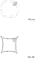
- the distortion in the microlens imaging process may include two main types: one type is barrel distortion, as shown in FIG. 8A .
- the other type is pin-cushion distortion, as shown in FIG. 8B .
- the dotted lines represent the ideal image of the imaging unit without distortion.
- the four small boxes represent four adjacent pixels.
- the distortion correction can be implemented in different ways and will be described in detail below.
- the light intensity of the first pixel may be corrected based on the light intensity of the first pixel and the light intensity of the three pixels whose second distance is smaller than the first distance of the first pixel to the center pixel.
- the coordinates of the first pixel are (i, j)
- the coordinates of the center pixel are (0, 0)
- the pixel (i, j-1) are pixels that are closer to the center pixel (0, 0) than the first pixel (i, j).
- the second distance of the three pixels from the center pixel is smaller than the first distance of the first pixel (i, j) from the center pixel (0, 0).
- This correction method is suitable for the image having the barrel distortion as shown in FIG. 8A .
- the light intensity of the first pixel can be corrected using the original light intensity of the first pixel and the light intensity of the three adjacent pixels closer to the center pixel than the first pixel so that the image having the barrel distortion can be corrected.
- the light intensity of the first pixel may be corrected based on the light intensity of the first pixel and the light intensity of the three pixels whose second distance is greater than the first distance of the first pixel to the center pixel.
- the coordinates of the first pixel are (i, j)
- the coordinates of the center pixel are (0, 0)
- the pixel (i+1, j+1) are pixels that are farther away from the center pixel (0, 0) than the first pixel (i, j).
- the second distance of the three pixels from the center pixel is greater than the first distance of the first pixel (i, j) from the center pixel (0, 0).
- This correction method is suitable for the image having the pin-cushion distortion as shown in FIG. 8B .
- the light intensity of the first pixel can be corrected using the original light intensity of the first pixel and the light intensity of the three adjacent pixels that are farther away from the center pixel than the first pixel so that the image having the pin-cushion distortion can be corrected.
- the present invention thus provides methods for correcting an image having distortion. It can be assuming that the size and trend of the distortion amount of each microlens are the same so that the processing efficiency of the image pattern can be improved.
- the present invention also provides a correction device for correcting image distortion.
- FIG. 10 is a simplified block diagram of an image distortion correction device according to an embodiment of the present invention.
- the image distortion correction device include an obtaining unit 1001, a first calculation unit 1002, a second calculation unit 1003, and a correction unit 1004.
- Obtaining unit 1001 is configured to obtain the light intensity of each pixel in an image including a plurality of pixels.
- the plurality of pixels may include a center pixel disposed at the center or near the center of the image and a first pixel different form the center pixel.
- First calculation unit 1002 is configured to calculate the first distance between the first pixel and the center pixel.
- Second calculation unit 1003 is configured to calculate a second distance between a second pixel and the first pixel, the second pixel may be at least a portion of the pixels adjacent to the first pixel.
- Correction unit 1004 is configured to correct the light intensity of the first pixel based on the original light intensity of the first pixel, the first distance, the second distance and the light intensity of the second pixel.
- the image distortion correction device can correct the light intensity of the first pixel using the originally obtained light intensity of the first pixel and of the second pixel that includes at least a portion of the pixels adjacent to the first pixel, so that the resulting image can be made closer to the actual image.
- the function of the image distortion correction device can be implemented by hardware (e.g., circuit logic, FPGA, one or more processing units) or by software having program code and instructions stored in a computer readable storage medium.
- correction unit 1004 may correct the light intensity of the first pixel using different approaches.
- the image may have a barrel distortion.
- the coordinates of the first pixel are (i, j)
- the coordinates of the center pixel are (0, 0)
- the pixel (i, j-1) are pixels that are closer to the center pixel (0, 0) than the first pixel (i, j). That is, the second distance of the three pixels from the center pixel is smaller than the first distance of the first pixel (i, j) from the center pixel (0, 0).
- the image may have a pin-cushion distortion.
- the coordinates of the first pixel are (i, j)
- the coordinates of the center pixel are (0, 0)
- the pixel (i+1, j+1) are pixels that are farther away from the center pixel (0, 0) than the first pixel (i, j). That is, the second distance of the three pixels from the center pixel is greater than the first distance of the first pixel (i, j) from the center pixel (0, 0).
- the present invention also provides a substrate surface defect detection device that may be any one of the above-described substrate surface defect detection devices and a device for correcting image distortion that may be one of the above-described image distortion correction devices.
- FIG. 11 is a simplified block diagram of a computing apparatus 1100 that may be programmed to execute codes for correcting image distortion according to one embodiment of the present invention.
- computing apparatus 1100 includes a processor having one or more processing units, a system memory, static storage units (hard drive), a display unit (LCD), an input device (keyboard, mouse, optical disc or magnetic tape reader, and the like).
- Computer apparatus 1100 also includes a network interface unit configured to connect the computing apparatus with other devices through a local area network, a wide area network, or a wireless network.
- the display unit has one or more windows for displaying the obtained light intensity of each pixel of an image, the image distortion and the corrected image.
- the input device may be connected to a digital camera for obtaining the light intensity of each pixel of an image.
- the processor is configured to calculate or compute the first distance between the first pixel and the center pixel, the second distance between the center pixel and the second pixel, and correct the light intensity of the first pixel based on the obtained light intensity of the first and second pixel, the first distance, and the second distance.
- the computing apparatus shown in FIG. 11 may include instruction codes that are stored in the system memory and executable by the processor to perform the above-described distance calculation and distortion correction.
- references in the specification to "one embodiment”, “an embodiment”, “an example embodiment”, “some embodiments”, etc., indicate that the embodiment described may include a particular feature, structure, or characteristic, but every embodiment may not necessarily include the particular feature, structure, or characteristic. Moreover, such phrases are not necessarily referring to the same embodiment. Further, when a particular feature, structure, or characteristic is described in connection with an embodiment, it is submitted that it is within the knowledge of one skilled in the art to affect such feature, structure, or characteristic in connection with other embodiments whether or not explicitly described.
Landscapes
- Engineering & Computer Science (AREA)
- Physics & Mathematics (AREA)
- General Physics & Mathematics (AREA)
- Theoretical Computer Science (AREA)
- Computer Vision & Pattern Recognition (AREA)
- Quality & Reliability (AREA)
- Analytical Chemistry (AREA)
- General Health & Medical Sciences (AREA)
- Immunology (AREA)
- Pathology (AREA)
- Biochemistry (AREA)
- Chemical & Material Sciences (AREA)
- Life Sciences & Earth Sciences (AREA)
- Health & Medical Sciences (AREA)
- Optics & Photonics (AREA)
- Investigating Materials By The Use Of Optical Means Adapted For Particular Applications (AREA)
- Geometry (AREA)
- Solid State Image Pick-Up Elements (AREA)
Applications Claiming Priority (1)
| Application Number | Priority Date | Filing Date | Title |
|---|---|---|---|
| CN201610826112.1A CN107845583B (zh) | 2016-09-18 | 2016-09-18 | 基板表面缺陷检测装置、图像畸变校正方法和装置以及基板表面缺陷检测设备 |
Publications (3)
| Publication Number | Publication Date |
|---|---|
| EP3296725A2 true EP3296725A2 (fr) | 2018-03-21 |
| EP3296725A3 EP3296725A3 (fr) | 2018-06-13 |
| EP3296725B1 EP3296725B1 (fr) | 2021-08-04 |
Family
ID=59895156
Family Applications (1)
| Application Number | Title | Priority Date | Filing Date |
|---|---|---|---|
| EP17191253.8A Active EP3296725B1 (fr) | 2016-09-18 | 2017-09-15 | Dispositif de détection de défauts de substrat faisant appel à une matrice de microlentilles |
Country Status (3)
| Country | Link |
|---|---|
| US (2) | US10416091B2 (fr) |
| EP (1) | EP3296725B1 (fr) |
| CN (1) | CN107845583B (fr) |
Cited By (2)
| Publication number | Priority date | Publication date | Assignee | Title |
|---|---|---|---|---|
| CN111292228A (zh) * | 2020-01-16 | 2020-06-16 | 宁波舜宇仪器有限公司 | 镜头缺陷检测方法 |
| CN115829977A (zh) * | 2022-12-09 | 2023-03-21 | 厦门大学 | 基于微透镜阵列曝光工艺的质量检测方法及参数调节方法 |
Families Citing this family (7)
| Publication number | Priority date | Publication date | Assignee | Title |
|---|---|---|---|---|
| CN107845583B (zh) | 2016-09-18 | 2020-12-18 | 中芯国际集成电路制造(上海)有限公司 | 基板表面缺陷检测装置、图像畸变校正方法和装置以及基板表面缺陷检测设备 |
| CN108734700B (zh) * | 2018-04-24 | 2021-06-11 | 信利(惠州)智能显示有限公司 | 基板盲区缺陷检测方法、装置、计算机和存储介质 |
| WO2019214064A1 (fr) * | 2018-05-11 | 2019-11-14 | 苏州源泽光电科技有限公司 | Dispositif de détection d'œil de mouche |
| JP7409988B2 (ja) * | 2020-07-29 | 2024-01-09 | 株式会社ニューフレアテクノロジー | パターン検査装置及び輪郭線同士のアライメント量取得方法 |
| KR102655947B1 (ko) * | 2020-09-03 | 2024-04-11 | 세메스 주식회사 | 기판 처리 장치 및 기판 처리 방법 |
| CN112596134B (zh) * | 2020-12-04 | 2022-03-22 | 西安交通大学 | 一种光波导微透镜阵列的制备及光学性能检测方法 |
| CN115629076B (zh) * | 2022-09-27 | 2025-02-18 | 威海华菱光电股份有限公司 | 一种阵列式图像检测装置 |
Family Cites Families (22)
| Publication number | Priority date | Publication date | Assignee | Title |
|---|---|---|---|---|
| JPH10289304A (ja) * | 1997-02-12 | 1998-10-27 | Nec Corp | 指紋画像入力装置 |
| US6611241B1 (en) * | 1997-12-02 | 2003-08-26 | Sarnoff Corporation | Modular display system |
| US6618494B1 (en) * | 1998-11-27 | 2003-09-09 | Wuestec Medical, Inc. | Optical distortion correction in digital imaging |
| US6538691B1 (en) * | 1999-01-21 | 2003-03-25 | Intel Corporation | Software correction of image distortion in digital cameras |
| US6192168B1 (en) * | 1999-04-09 | 2001-02-20 | The United States Of America As Represented By The Secretary Of The Navy | Reflectively coated optical waveguide and fluidics cell integration |
| US6924816B2 (en) * | 2000-03-17 | 2005-08-02 | Sun Microsystems, Inc. | Compensating for the chromatic distortion of displayed images |
| JP2004327713A (ja) * | 2003-04-24 | 2004-11-18 | Sharp Corp | 画像読取装置及びその製造方法 |
| US7079251B2 (en) * | 2003-10-16 | 2006-07-18 | 4D Technology Corporation | Calibration and error correction in multi-channel imaging |
| GB0326005D0 (en) * | 2003-11-07 | 2003-12-10 | Koninkl Philips Electronics Nv | Waveguide for autostereoscopic display |
| US7399421B2 (en) * | 2005-08-02 | 2008-07-15 | International Business Machines Corporation | Injection molded microoptics |
| US20070126892A1 (en) * | 2005-11-30 | 2007-06-07 | Haike Guan | Correcting an image captured through a lens |
| BRPI0908090A2 (pt) * | 2008-02-25 | 2015-08-25 | Koninkl Philips Electronics Nv | Sensor óptico e método para medir luz irradia de um analito mediante excitação da luz, e, kit de partes |
| US8618508B2 (en) * | 2008-09-25 | 2013-12-31 | Koninklijke Philips N.V. | Detection system and method |
| DK2391451T3 (en) * | 2009-02-02 | 2018-10-15 | Opko Diagnostics Llc | STRUCTURES FOR MANAGING LIGHT INTERACTION WITH MICROFLUIDIC DEVICES |
| US8274583B2 (en) * | 2009-06-05 | 2012-09-25 | Apple Inc. | Radially-based chroma noise reduction for cameras |
| CN102256100B (zh) * | 2011-07-19 | 2013-02-13 | 中国科学技术大学 | 基于微透镜阵列和平板显示集成的双向成像-显示系统 |
| US20150010265A1 (en) * | 2012-01-06 | 2015-01-08 | Milan, Momcilo POPOVICH | Contact image sensor using switchable bragg gratings |
| JP6321953B2 (ja) * | 2013-12-05 | 2018-05-09 | 株式会社日立エルジーデータストレージ | レーザ投射表示装置 |
| TWI511086B (zh) * | 2014-04-18 | 2015-12-01 | Altek Semiconductor Corp | 鏡頭失真校正方法 |
| JP2017112514A (ja) * | 2015-12-17 | 2017-06-22 | ソニー株式会社 | 信号処理方法、及び撮像装置 |
| CN107924558B (zh) * | 2016-03-14 | 2019-04-30 | Realop株式会社 | 图像处理装置、图像处理方法、记录介质以及拍摄装置 |
| CN107845583B (zh) | 2016-09-18 | 2020-12-18 | 中芯国际集成电路制造(上海)有限公司 | 基板表面缺陷检测装置、图像畸变校正方法和装置以及基板表面缺陷检测设备 |
-
2016
- 2016-09-18 CN CN201610826112.1A patent/CN107845583B/zh active Active
-
2017
- 2017-09-15 EP EP17191253.8A patent/EP3296725B1/fr active Active
- 2017-09-15 US US15/706,409 patent/US10416091B2/en active Active
-
2019
- 2019-07-26 US US16/523,859 patent/US11085884B2/en active Active
Non-Patent Citations (1)
| Title |
|---|
| None |
Cited By (3)
| Publication number | Priority date | Publication date | Assignee | Title |
|---|---|---|---|---|
| CN111292228A (zh) * | 2020-01-16 | 2020-06-16 | 宁波舜宇仪器有限公司 | 镜头缺陷检测方法 |
| CN111292228B (zh) * | 2020-01-16 | 2023-08-11 | 宁波舜宇仪器有限公司 | 镜头缺陷检测方法 |
| CN115829977A (zh) * | 2022-12-09 | 2023-03-21 | 厦门大学 | 基于微透镜阵列曝光工艺的质量检测方法及参数调节方法 |
Also Published As
| Publication number | Publication date |
|---|---|
| US20190346377A1 (en) | 2019-11-14 |
| CN107845583B (zh) | 2020-12-18 |
| EP3296725B1 (fr) | 2021-08-04 |
| US20180080883A1 (en) | 2018-03-22 |
| EP3296725A3 (fr) | 2018-06-13 |
| CN107845583A (zh) | 2018-03-27 |
| US10416091B2 (en) | 2019-09-17 |
| US11085884B2 (en) | 2021-08-10 |
Similar Documents
| Publication | Publication Date | Title |
|---|---|---|
| US11085884B2 (en) | Defect inspection method and apparatus using micro lens matrix | |
| US9524565B2 (en) | Method of freeform imaging system | |
| US8793104B2 (en) | Flat panel display device | |
| CN105974427B (zh) | 结构光测距装置及方法 | |
| US9440451B2 (en) | 2-D straight-scan on imaging surface with a raster polygon | |
| US8102603B2 (en) | Lens having extended depth of focus, method for designing the same, and optical system having the same | |
| CN119937255A (zh) | 光学系统和方法 | |
| US9494531B2 (en) | Multi-spot illumination for improved detection sensitivity | |
| CN106133898A (zh) | 用于对象检验的可变图像场曲率 | |
| US9810640B2 (en) | Panel inspection apparatus and method | |
| US10976670B2 (en) | Apparatus and method for detecting optimal focal plane of lithographic projection objective lens | |
| US20230117164A1 (en) | Diffuser device | |
| TWI616967B (zh) | 在斜面上產生一點陣列 | |
| US10801890B1 (en) | Measurement system and a method of diffracting light | |
| US3743423A (en) | Intensity spatial filter having uniformly spaced filter elements | |
| US20200292836A1 (en) | Apparatus for forming a homogeneous intensity distribution with bright or dark edges | |
| TWI876107B (zh) | 微陣列型擴散板 | |
| EP3729183B1 (fr) | Système d'éclairage pour projection de lumière | |
| CN105980933B (zh) | 射束曝光装置 | |
| US11016034B2 (en) | Optical scattering measurement method and apparatus using micro lens matrix | |
| JP2009503593A (ja) | 線焦点を作成する光学システム、この光学システムを用いる走査システム、および基板のレーザ加工方法 | |
| US3738752A (en) | Intensity spatial filter having non-uniformly spaced filter elements | |
| JP7719512B2 (ja) | テラヘルツ光源、流体検知器、及び、テラヘルツ波生成方法 | |
| JPS5815767B2 (ja) | ヒカリビ−ムソウサホセイコウガクケイ | |
| JP6471031B2 (ja) | 位相フィルタ、撮像光学系、及び撮像システム |
Legal Events
| Date | Code | Title | Description |
|---|---|---|---|
| PUAI | Public reference made under article 153(3) epc to a published international application that has entered the european phase |
Free format text: ORIGINAL CODE: 0009012 |
|
| STAA | Information on the status of an ep patent application or granted ep patent |
Free format text: STATUS: THE APPLICATION HAS BEEN PUBLISHED |
|
| AK | Designated contracting states |
Kind code of ref document: A2 Designated state(s): AL AT BE BG CH CY CZ DE DK EE ES FI FR GB GR HR HU IE IS IT LI LT LU LV MC MK MT NL NO PL PT RO RS SE SI SK SM TR |
|
| AX | Request for extension of the european patent |
Extension state: BA ME |
|
| RIC1 | Information provided on ipc code assigned before grant |
Ipc: G02B 3/00 20060101ALI20180312BHEP Ipc: G01N 21/956 20060101AFI20180312BHEP Ipc: G06T 5/00 20060101ALI20180312BHEP |
|
| PUAL | Search report despatched |
Free format text: ORIGINAL CODE: 0009013 |
|
| AK | Designated contracting states |
Kind code of ref document: A3 Designated state(s): AL AT BE BG CH CY CZ DE DK EE ES FI FR GB GR HR HU IE IS IT LI LT LU LV MC MK MT NL NO PL PT RO RS SE SI SK SM TR |
|
| AX | Request for extension of the european patent |
Extension state: BA ME |
|
| RIC1 | Information provided on ipc code assigned before grant |
Ipc: G01N 21/88 20060101ALI20180508BHEP Ipc: G01N 21/95 20060101ALI20180508BHEP Ipc: H04N 3/233 20060101ALI20180508BHEP Ipc: G01N 21/956 20060101AFI20180508BHEP Ipc: G06T 7/00 20170101ALI20180508BHEP Ipc: G06T 5/00 20060101ALI20180508BHEP Ipc: G02B 3/00 20060101ALI20180508BHEP |
|
| RAP1 | Party data changed (applicant data changed or rights of an application transferred) |
Owner name: SEMICONDUCTOR MANUFACTURING INTERNATIONAL (BEIJING Owner name: SEMICONDUCTOR MANUFACTURING INTERNATIONAL (SHANGHA |
|
| STAA | Information on the status of an ep patent application or granted ep patent |
Free format text: STATUS: REQUEST FOR EXAMINATION WAS MADE |
|
| 17P | Request for examination filed |
Effective date: 20181204 |
|
| RBV | Designated contracting states (corrected) |
Designated state(s): AL AT BE BG CH CY CZ DE DK EE ES FI FR GB GR HR HU IE IS IT LI LT LU LV MC MK MT NL NO PL PT RO RS SE SI SK SM TR |
|
| REG | Reference to a national code |
Ref country code: DE Ref legal event code: R079 Ref document number: 602017043251 Country of ref document: DE Free format text: PREVIOUS MAIN CLASS: G01N0021956000 Ipc: H01L0021660000 |
|
| GRAP | Despatch of communication of intention to grant a patent |
Free format text: ORIGINAL CODE: EPIDOSNIGR1 |
|
| STAA | Information on the status of an ep patent application or granted ep patent |
Free format text: STATUS: GRANT OF PATENT IS INTENDED |
|
| RIC1 | Information provided on ipc code assigned before grant |
Ipc: G06T 5/00 20060101ALI20210222BHEP Ipc: G06T 7/00 20170101ALI20210222BHEP Ipc: G01N 21/956 20060101ALI20210222BHEP Ipc: H01L 21/66 20060101AFI20210222BHEP |
|
| INTG | Intention to grant announced |
Effective date: 20210312 |
|
| GRAS | Grant fee paid |
Free format text: ORIGINAL CODE: EPIDOSNIGR3 |
|
| GRAA | (expected) grant |
Free format text: ORIGINAL CODE: 0009210 |
|
| STAA | Information on the status of an ep patent application or granted ep patent |
Free format text: STATUS: THE PATENT HAS BEEN GRANTED |
|
| AK | Designated contracting states |
Kind code of ref document: B1 Designated state(s): AL AT BE BG CH CY CZ DE DK EE ES FI FR GB GR HR HU IE IS IT LI LT LU LV MC MK MT NL NO PL PT RO RS SE SI SK SM TR |
|
| REG | Reference to a national code |
Ref country code: GB Ref legal event code: FG4D |
|
| REG | Reference to a national code |
Ref country code: AT Ref legal event code: REF Ref document number: 1417852 Country of ref document: AT Kind code of ref document: T Effective date: 20210815 |
|
| REG | Reference to a national code |
Ref country code: CH Ref legal event code: EP |
|
| REG | Reference to a national code |
Ref country code: DE Ref legal event code: R096 Ref document number: 602017043251 Country of ref document: DE |
|
| REG | Reference to a national code |
Ref country code: IE Ref legal event code: FG4D |
|
| REG | Reference to a national code |
Ref country code: LT Ref legal event code: MG9D |
|
| REG | Reference to a national code |
Ref country code: NL Ref legal event code: MP Effective date: 20210804 |
|
| REG | Reference to a national code |
Ref country code: AT Ref legal event code: MK05 Ref document number: 1417852 Country of ref document: AT Kind code of ref document: T Effective date: 20210804 |
|
| PG25 | Lapsed in a contracting state [announced via postgrant information from national office to epo] |
Ref country code: SE Free format text: LAPSE BECAUSE OF FAILURE TO SUBMIT A TRANSLATION OF THE DESCRIPTION OR TO PAY THE FEE WITHIN THE PRESCRIBED TIME-LIMIT Effective date: 20210804 Ref country code: RS Free format text: LAPSE BECAUSE OF FAILURE TO SUBMIT A TRANSLATION OF THE DESCRIPTION OR TO PAY THE FEE WITHIN THE PRESCRIBED TIME-LIMIT Effective date: 20210804 Ref country code: HR Free format text: LAPSE BECAUSE OF FAILURE TO SUBMIT A TRANSLATION OF THE DESCRIPTION OR TO PAY THE FEE WITHIN THE PRESCRIBED TIME-LIMIT Effective date: 20210804 Ref country code: LT Free format text: LAPSE BECAUSE OF FAILURE TO SUBMIT A TRANSLATION OF THE DESCRIPTION OR TO PAY THE FEE WITHIN THE PRESCRIBED TIME-LIMIT Effective date: 20210804 Ref country code: AT Free format text: LAPSE BECAUSE OF FAILURE TO SUBMIT A TRANSLATION OF THE DESCRIPTION OR TO PAY THE FEE WITHIN THE PRESCRIBED TIME-LIMIT Effective date: 20210804 Ref country code: BG Free format text: LAPSE BECAUSE OF FAILURE TO SUBMIT A TRANSLATION OF THE DESCRIPTION OR TO PAY THE FEE WITHIN THE PRESCRIBED TIME-LIMIT Effective date: 20211104 Ref country code: NO Free format text: LAPSE BECAUSE OF FAILURE TO SUBMIT A TRANSLATION OF THE DESCRIPTION OR TO PAY THE FEE WITHIN THE PRESCRIBED TIME-LIMIT Effective date: 20211104 Ref country code: PT Free format text: LAPSE BECAUSE OF FAILURE TO SUBMIT A TRANSLATION OF THE DESCRIPTION OR TO PAY THE FEE WITHIN THE PRESCRIBED TIME-LIMIT Effective date: 20211206 Ref country code: FI Free format text: LAPSE BECAUSE OF FAILURE TO SUBMIT A TRANSLATION OF THE DESCRIPTION OR TO PAY THE FEE WITHIN THE PRESCRIBED TIME-LIMIT Effective date: 20210804 Ref country code: ES Free format text: LAPSE BECAUSE OF FAILURE TO SUBMIT A TRANSLATION OF THE DESCRIPTION OR TO PAY THE FEE WITHIN THE PRESCRIBED TIME-LIMIT Effective date: 20210804 |
|
| PG25 | Lapsed in a contracting state [announced via postgrant information from national office to epo] |
Ref country code: PL Free format text: LAPSE BECAUSE OF FAILURE TO SUBMIT A TRANSLATION OF THE DESCRIPTION OR TO PAY THE FEE WITHIN THE PRESCRIBED TIME-LIMIT Effective date: 20210804 Ref country code: LV Free format text: LAPSE BECAUSE OF FAILURE TO SUBMIT A TRANSLATION OF THE DESCRIPTION OR TO PAY THE FEE WITHIN THE PRESCRIBED TIME-LIMIT Effective date: 20210804 Ref country code: GR Free format text: LAPSE BECAUSE OF FAILURE TO SUBMIT A TRANSLATION OF THE DESCRIPTION OR TO PAY THE FEE WITHIN THE PRESCRIBED TIME-LIMIT Effective date: 20211105 |
|
| REG | Reference to a national code |
Ref country code: DE Ref legal event code: R119 Ref document number: 602017043251 Country of ref document: DE |
|
| PG25 | Lapsed in a contracting state [announced via postgrant information from national office to epo] |
Ref country code: NL Free format text: LAPSE BECAUSE OF FAILURE TO SUBMIT A TRANSLATION OF THE DESCRIPTION OR TO PAY THE FEE WITHIN THE PRESCRIBED TIME-LIMIT Effective date: 20210804 |
|
| PG25 | Lapsed in a contracting state [announced via postgrant information from national office to epo] |
Ref country code: DK Free format text: LAPSE BECAUSE OF FAILURE TO SUBMIT A TRANSLATION OF THE DESCRIPTION OR TO PAY THE FEE WITHIN THE PRESCRIBED TIME-LIMIT Effective date: 20210804 |
|
| REG | Reference to a national code |
Ref country code: CH Ref legal event code: PL |
|
| REG | Reference to a national code |
Ref country code: BE Ref legal event code: MM Effective date: 20210930 |
|
| PG25 | Lapsed in a contracting state [announced via postgrant information from national office to epo] |
Ref country code: SM Free format text: LAPSE BECAUSE OF FAILURE TO SUBMIT A TRANSLATION OF THE DESCRIPTION OR TO PAY THE FEE WITHIN THE PRESCRIBED TIME-LIMIT Effective date: 20210804 Ref country code: SK Free format text: LAPSE BECAUSE OF FAILURE TO SUBMIT A TRANSLATION OF THE DESCRIPTION OR TO PAY THE FEE WITHIN THE PRESCRIBED TIME-LIMIT Effective date: 20210804 Ref country code: RO Free format text: LAPSE BECAUSE OF FAILURE TO SUBMIT A TRANSLATION OF THE DESCRIPTION OR TO PAY THE FEE WITHIN THE PRESCRIBED TIME-LIMIT Effective date: 20210804 Ref country code: MC Free format text: LAPSE BECAUSE OF FAILURE TO SUBMIT A TRANSLATION OF THE DESCRIPTION OR TO PAY THE FEE WITHIN THE PRESCRIBED TIME-LIMIT Effective date: 20210804 Ref country code: EE Free format text: LAPSE BECAUSE OF FAILURE TO SUBMIT A TRANSLATION OF THE DESCRIPTION OR TO PAY THE FEE WITHIN THE PRESCRIBED TIME-LIMIT Effective date: 20210804 Ref country code: CZ Free format text: LAPSE BECAUSE OF FAILURE TO SUBMIT A TRANSLATION OF THE DESCRIPTION OR TO PAY THE FEE WITHIN THE PRESCRIBED TIME-LIMIT Effective date: 20210804 Ref country code: AL Free format text: LAPSE BECAUSE OF FAILURE TO SUBMIT A TRANSLATION OF THE DESCRIPTION OR TO PAY THE FEE WITHIN THE PRESCRIBED TIME-LIMIT Effective date: 20210804 |
|
| PLBE | No opposition filed within time limit |
Free format text: ORIGINAL CODE: 0009261 |
|
| STAA | Information on the status of an ep patent application or granted ep patent |
Free format text: STATUS: NO OPPOSITION FILED WITHIN TIME LIMIT |
|
| 26N | No opposition filed |
Effective date: 20220506 |
|
| GBPC | Gb: european patent ceased through non-payment of renewal fee |
Effective date: 20211104 |
|
| PG25 | Lapsed in a contracting state [announced via postgrant information from national office to epo] |
Ref country code: LU Free format text: LAPSE BECAUSE OF NON-PAYMENT OF DUE FEES Effective date: 20210915 Ref country code: IT Free format text: LAPSE BECAUSE OF FAILURE TO SUBMIT A TRANSLATION OF THE DESCRIPTION OR TO PAY THE FEE WITHIN THE PRESCRIBED TIME-LIMIT Effective date: 20210804 Ref country code: IE Free format text: LAPSE BECAUSE OF NON-PAYMENT OF DUE FEES Effective date: 20210915 Ref country code: DE Free format text: LAPSE BECAUSE OF NON-PAYMENT OF DUE FEES Effective date: 20220401 Ref country code: BE Free format text: LAPSE BECAUSE OF NON-PAYMENT OF DUE FEES Effective date: 20210930 |
|
| PG25 | Lapsed in a contracting state [announced via postgrant information from national office to epo] |
Ref country code: SI Free format text: LAPSE BECAUSE OF FAILURE TO SUBMIT A TRANSLATION OF THE DESCRIPTION OR TO PAY THE FEE WITHIN THE PRESCRIBED TIME-LIMIT Effective date: 20210804 Ref country code: LI Free format text: LAPSE BECAUSE OF NON-PAYMENT OF DUE FEES Effective date: 20210930 Ref country code: CH Free format text: LAPSE BECAUSE OF NON-PAYMENT OF DUE FEES Effective date: 20210930 |
|
| PG25 | Lapsed in a contracting state [announced via postgrant information from national office to epo] |
Ref country code: FR Free format text: LAPSE BECAUSE OF NON-PAYMENT OF DUE FEES Effective date: 20211004 |
|
| PG25 | Lapsed in a contracting state [announced via postgrant information from national office to epo] |
Ref country code: GB Free format text: LAPSE BECAUSE OF NON-PAYMENT OF DUE FEES Effective date: 20211104 |
|
| PG25 | Lapsed in a contracting state [announced via postgrant information from national office to epo] |
Ref country code: HU Free format text: LAPSE BECAUSE OF FAILURE TO SUBMIT A TRANSLATION OF THE DESCRIPTION OR TO PAY THE FEE WITHIN THE PRESCRIBED TIME-LIMIT; INVALID AB INITIO Effective date: 20170915 |
|
| PG25 | Lapsed in a contracting state [announced via postgrant information from national office to epo] |
Ref country code: CY Free format text: LAPSE BECAUSE OF FAILURE TO SUBMIT A TRANSLATION OF THE DESCRIPTION OR TO PAY THE FEE WITHIN THE PRESCRIBED TIME-LIMIT Effective date: 20210804 |
|
| PG25 | Lapsed in a contracting state [announced via postgrant information from national office to epo] |
Ref country code: MK Free format text: LAPSE BECAUSE OF FAILURE TO SUBMIT A TRANSLATION OF THE DESCRIPTION OR TO PAY THE FEE WITHIN THE PRESCRIBED TIME-LIMIT Effective date: 20210804 |
|
| PG25 | Lapsed in a contracting state [announced via postgrant information from national office to epo] |
Ref country code: TR Free format text: LAPSE BECAUSE OF FAILURE TO SUBMIT A TRANSLATION OF THE DESCRIPTION OR TO PAY THE FEE WITHIN THE PRESCRIBED TIME-LIMIT Effective date: 20210804 |
|
| PG25 | Lapsed in a contracting state [announced via postgrant information from national office to epo] |
Ref country code: MT Free format text: LAPSE BECAUSE OF FAILURE TO SUBMIT A TRANSLATION OF THE DESCRIPTION OR TO PAY THE FEE WITHIN THE PRESCRIBED TIME-LIMIT Effective date: 20210804 |