EP3296983A1 - Circuit de pixels oled, dispositif d'affichage et procédé de commande - Google Patents
Circuit de pixels oled, dispositif d'affichage et procédé de commande Download PDFInfo
- Publication number
- EP3296983A1 EP3296983A1 EP15851606.2A EP15851606A EP3296983A1 EP 3296983 A1 EP3296983 A1 EP 3296983A1 EP 15851606 A EP15851606 A EP 15851606A EP 3296983 A1 EP3296983 A1 EP 3296983A1
- Authority
- EP
- European Patent Office
- Prior art keywords
- driving transistor
- oled
- reference signal
- switching unit
- circuit
- Prior art date
- Legal status (The legal status is an assumption and is not a legal conclusion. Google has not performed a legal analysis and makes no representation as to the accuracy of the status listed.)
- Granted
Links
Images



Classifications
-
- G—PHYSICS
- G09—EDUCATION; CRYPTOGRAPHY; DISPLAY; ADVERTISING; SEALS
- G09G—ARRANGEMENTS OR CIRCUITS FOR CONTROL OF INDICATING DEVICES USING STATIC MEANS TO PRESENT VARIABLE INFORMATION
- G09G3/00—Control arrangements or circuits, of interest only in connection with visual indicators other than cathode-ray tubes
- G09G3/20—Control arrangements or circuits, of interest only in connection with visual indicators other than cathode-ray tubes for presentation of an assembly of a number of characters, e.g. a page, by composing the assembly by combination of individual elements arranged in a matrix no fixed position being assigned to or needed to be assigned to the individual characters or partial characters
- G09G3/22—Control arrangements or circuits, of interest only in connection with visual indicators other than cathode-ray tubes for presentation of an assembly of a number of characters, e.g. a page, by composing the assembly by combination of individual elements arranged in a matrix no fixed position being assigned to or needed to be assigned to the individual characters or partial characters using controlled light sources
- G09G3/30—Control arrangements or circuits, of interest only in connection with visual indicators other than cathode-ray tubes for presentation of an assembly of a number of characters, e.g. a page, by composing the assembly by combination of individual elements arranged in a matrix no fixed position being assigned to or needed to be assigned to the individual characters or partial characters using controlled light sources using electroluminescent panels
- G09G3/32—Control arrangements or circuits, of interest only in connection with visual indicators other than cathode-ray tubes for presentation of an assembly of a number of characters, e.g. a page, by composing the assembly by combination of individual elements arranged in a matrix no fixed position being assigned to or needed to be assigned to the individual characters or partial characters using controlled light sources using electroluminescent panels semiconductive, e.g. using light-emitting diodes [LED]
- G09G3/3208—Control arrangements or circuits, of interest only in connection with visual indicators other than cathode-ray tubes for presentation of an assembly of a number of characters, e.g. a page, by composing the assembly by combination of individual elements arranged in a matrix no fixed position being assigned to or needed to be assigned to the individual characters or partial characters using controlled light sources using electroluminescent panels semiconductive, e.g. using light-emitting diodes [LED] organic, e.g. using organic light-emitting diodes [OLED]
- G09G3/3225—Control arrangements or circuits, of interest only in connection with visual indicators other than cathode-ray tubes for presentation of an assembly of a number of characters, e.g. a page, by composing the assembly by combination of individual elements arranged in a matrix no fixed position being assigned to or needed to be assigned to the individual characters or partial characters using controlled light sources using electroluminescent panels semiconductive, e.g. using light-emitting diodes [LED] organic, e.g. using organic light-emitting diodes [OLED] using an active matrix
- G09G3/3233—Control arrangements or circuits, of interest only in connection with visual indicators other than cathode-ray tubes for presentation of an assembly of a number of characters, e.g. a page, by composing the assembly by combination of individual elements arranged in a matrix no fixed position being assigned to or needed to be assigned to the individual characters or partial characters using controlled light sources using electroluminescent panels semiconductive, e.g. using light-emitting diodes [LED] organic, e.g. using organic light-emitting diodes [OLED] using an active matrix with pixel circuitry controlling the current through the light-emitting element
- G09G3/3241—Control arrangements or circuits, of interest only in connection with visual indicators other than cathode-ray tubes for presentation of an assembly of a number of characters, e.g. a page, by composing the assembly by combination of individual elements arranged in a matrix no fixed position being assigned to or needed to be assigned to the individual characters or partial characters using controlled light sources using electroluminescent panels semiconductive, e.g. using light-emitting diodes [LED] organic, e.g. using organic light-emitting diodes [OLED] using an active matrix with pixel circuitry controlling the current through the light-emitting element the current through the light-emitting element being set using a data current provided by the data driver, e.g. by using a two-transistor current mirror
- G09G3/325—Control arrangements or circuits, of interest only in connection with visual indicators other than cathode-ray tubes for presentation of an assembly of a number of characters, e.g. a page, by composing the assembly by combination of individual elements arranged in a matrix no fixed position being assigned to or needed to be assigned to the individual characters or partial characters using controlled light sources using electroluminescent panels semiconductive, e.g. using light-emitting diodes [LED] organic, e.g. using organic light-emitting diodes [OLED] using an active matrix with pixel circuitry controlling the current through the light-emitting element the current through the light-emitting element being set using a data current provided by the data driver, e.g. by using a two-transistor current mirror the data current flowing through the driving transistor during a setting phase, e.g. by using a switch for connecting the driving transistor to the data driver
-
- G—PHYSICS
- G09—EDUCATION; CRYPTOGRAPHY; DISPLAY; ADVERTISING; SEALS
- G09G—ARRANGEMENTS OR CIRCUITS FOR CONTROL OF INDICATING DEVICES USING STATIC MEANS TO PRESENT VARIABLE INFORMATION
- G09G3/00—Control arrangements or circuits, of interest only in connection with visual indicators other than cathode-ray tubes
- G09G3/20—Control arrangements or circuits, of interest only in connection with visual indicators other than cathode-ray tubes for presentation of an assembly of a number of characters, e.g. a page, by composing the assembly by combination of individual elements arranged in a matrix no fixed position being assigned to or needed to be assigned to the individual characters or partial characters
- G09G3/22—Control arrangements or circuits, of interest only in connection with visual indicators other than cathode-ray tubes for presentation of an assembly of a number of characters, e.g. a page, by composing the assembly by combination of individual elements arranged in a matrix no fixed position being assigned to or needed to be assigned to the individual characters or partial characters using controlled light sources
- G09G3/30—Control arrangements or circuits, of interest only in connection with visual indicators other than cathode-ray tubes for presentation of an assembly of a number of characters, e.g. a page, by composing the assembly by combination of individual elements arranged in a matrix no fixed position being assigned to or needed to be assigned to the individual characters or partial characters using controlled light sources using electroluminescent panels
- G09G3/32—Control arrangements or circuits, of interest only in connection with visual indicators other than cathode-ray tubes for presentation of an assembly of a number of characters, e.g. a page, by composing the assembly by combination of individual elements arranged in a matrix no fixed position being assigned to or needed to be assigned to the individual characters or partial characters using controlled light sources using electroluminescent panels semiconductive, e.g. using light-emitting diodes [LED]
- G09G3/3208—Control arrangements or circuits, of interest only in connection with visual indicators other than cathode-ray tubes for presentation of an assembly of a number of characters, e.g. a page, by composing the assembly by combination of individual elements arranged in a matrix no fixed position being assigned to or needed to be assigned to the individual characters or partial characters using controlled light sources using electroluminescent panels semiconductive, e.g. using light-emitting diodes [LED] organic, e.g. using organic light-emitting diodes [OLED]
- G09G3/3225—Control arrangements or circuits, of interest only in connection with visual indicators other than cathode-ray tubes for presentation of an assembly of a number of characters, e.g. a page, by composing the assembly by combination of individual elements arranged in a matrix no fixed position being assigned to or needed to be assigned to the individual characters or partial characters using controlled light sources using electroluminescent panels semiconductive, e.g. using light-emitting diodes [LED] organic, e.g. using organic light-emitting diodes [OLED] using an active matrix
- G09G3/3233—Control arrangements or circuits, of interest only in connection with visual indicators other than cathode-ray tubes for presentation of an assembly of a number of characters, e.g. a page, by composing the assembly by combination of individual elements arranged in a matrix no fixed position being assigned to or needed to be assigned to the individual characters or partial characters using controlled light sources using electroluminescent panels semiconductive, e.g. using light-emitting diodes [LED] organic, e.g. using organic light-emitting diodes [OLED] using an active matrix with pixel circuitry controlling the current through the light-emitting element
-
- G—PHYSICS
- G09—EDUCATION; CRYPTOGRAPHY; DISPLAY; ADVERTISING; SEALS
- G09G—ARRANGEMENTS OR CIRCUITS FOR CONTROL OF INDICATING DEVICES USING STATIC MEANS TO PRESENT VARIABLE INFORMATION
- G09G3/00—Control arrangements or circuits, of interest only in connection with visual indicators other than cathode-ray tubes
- G09G3/20—Control arrangements or circuits, of interest only in connection with visual indicators other than cathode-ray tubes for presentation of an assembly of a number of characters, e.g. a page, by composing the assembly by combination of individual elements arranged in a matrix no fixed position being assigned to or needed to be assigned to the individual characters or partial characters
- G09G3/22—Control arrangements or circuits, of interest only in connection with visual indicators other than cathode-ray tubes for presentation of an assembly of a number of characters, e.g. a page, by composing the assembly by combination of individual elements arranged in a matrix no fixed position being assigned to or needed to be assigned to the individual characters or partial characters using controlled light sources
- G09G3/30—Control arrangements or circuits, of interest only in connection with visual indicators other than cathode-ray tubes for presentation of an assembly of a number of characters, e.g. a page, by composing the assembly by combination of individual elements arranged in a matrix no fixed position being assigned to or needed to be assigned to the individual characters or partial characters using controlled light sources using electroluminescent panels
- G09G3/32—Control arrangements or circuits, of interest only in connection with visual indicators other than cathode-ray tubes for presentation of an assembly of a number of characters, e.g. a page, by composing the assembly by combination of individual elements arranged in a matrix no fixed position being assigned to or needed to be assigned to the individual characters or partial characters using controlled light sources using electroluminescent panels semiconductive, e.g. using light-emitting diodes [LED]
-
- G—PHYSICS
- G09—EDUCATION; CRYPTOGRAPHY; DISPLAY; ADVERTISING; SEALS
- G09G—ARRANGEMENTS OR CIRCUITS FOR CONTROL OF INDICATING DEVICES USING STATIC MEANS TO PRESENT VARIABLE INFORMATION
- G09G3/00—Control arrangements or circuits, of interest only in connection with visual indicators other than cathode-ray tubes
- G09G3/20—Control arrangements or circuits, of interest only in connection with visual indicators other than cathode-ray tubes for presentation of an assembly of a number of characters, e.g. a page, by composing the assembly by combination of individual elements arranged in a matrix no fixed position being assigned to or needed to be assigned to the individual characters or partial characters
- G09G3/22—Control arrangements or circuits, of interest only in connection with visual indicators other than cathode-ray tubes for presentation of an assembly of a number of characters, e.g. a page, by composing the assembly by combination of individual elements arranged in a matrix no fixed position being assigned to or needed to be assigned to the individual characters or partial characters using controlled light sources
- G09G3/30—Control arrangements or circuits, of interest only in connection with visual indicators other than cathode-ray tubes for presentation of an assembly of a number of characters, e.g. a page, by composing the assembly by combination of individual elements arranged in a matrix no fixed position being assigned to or needed to be assigned to the individual characters or partial characters using controlled light sources using electroluminescent panels
- G09G3/32—Control arrangements or circuits, of interest only in connection with visual indicators other than cathode-ray tubes for presentation of an assembly of a number of characters, e.g. a page, by composing the assembly by combination of individual elements arranged in a matrix no fixed position being assigned to or needed to be assigned to the individual characters or partial characters using controlled light sources using electroluminescent panels semiconductive, e.g. using light-emitting diodes [LED]
- G09G3/3208—Control arrangements or circuits, of interest only in connection with visual indicators other than cathode-ray tubes for presentation of an assembly of a number of characters, e.g. a page, by composing the assembly by combination of individual elements arranged in a matrix no fixed position being assigned to or needed to be assigned to the individual characters or partial characters using controlled light sources using electroluminescent panels semiconductive, e.g. using light-emitting diodes [LED] organic, e.g. using organic light-emitting diodes [OLED]
- G09G3/3275—Details of drivers for data electrodes
- G09G3/3291—Details of drivers for data electrodes in which the data driver supplies a variable data voltage for setting the current through, or the voltage across, the light-emitting elements
-
- G—PHYSICS
- G09—EDUCATION; CRYPTOGRAPHY; DISPLAY; ADVERTISING; SEALS
- G09G—ARRANGEMENTS OR CIRCUITS FOR CONTROL OF INDICATING DEVICES USING STATIC MEANS TO PRESENT VARIABLE INFORMATION
- G09G2300/00—Aspects of the constitution of display devices
- G09G2300/08—Active matrix structure, i.e. with use of active elements, inclusive of non-linear two terminal elements, in the pixels together with light emitting or modulating elements
- G09G2300/0809—Several active elements per pixel in active matrix panels
- G09G2300/0819—Several active elements per pixel in active matrix panels used for counteracting undesired variations, e.g. feedback or autozeroing
-
- G—PHYSICS
- G09—EDUCATION; CRYPTOGRAPHY; DISPLAY; ADVERTISING; SEALS
- G09G—ARRANGEMENTS OR CIRCUITS FOR CONTROL OF INDICATING DEVICES USING STATIC MEANS TO PRESENT VARIABLE INFORMATION
- G09G2300/00—Aspects of the constitution of display devices
- G09G2300/08—Active matrix structure, i.e. with use of active elements, inclusive of non-linear two terminal elements, in the pixels together with light emitting or modulating elements
- G09G2300/0809—Several active elements per pixel in active matrix panels
- G09G2300/0842—Several active elements per pixel in active matrix panels forming a memory circuit, e.g. a dynamic memory with one capacitor
- G09G2300/0852—Several active elements per pixel in active matrix panels forming a memory circuit, e.g. a dynamic memory with one capacitor being a dynamic memory with more than one capacitor
-
- G—PHYSICS
- G09—EDUCATION; CRYPTOGRAPHY; DISPLAY; ADVERTISING; SEALS
- G09G—ARRANGEMENTS OR CIRCUITS FOR CONTROL OF INDICATING DEVICES USING STATIC MEANS TO PRESENT VARIABLE INFORMATION
- G09G2300/00—Aspects of the constitution of display devices
- G09G2300/08—Active matrix structure, i.e. with use of active elements, inclusive of non-linear two terminal elements, in the pixels together with light emitting or modulating elements
- G09G2300/0809—Several active elements per pixel in active matrix panels
- G09G2300/0842—Several active elements per pixel in active matrix panels forming a memory circuit, e.g. a dynamic memory with one capacitor
- G09G2300/0861—Several active elements per pixel in active matrix panels forming a memory circuit, e.g. a dynamic memory with one capacitor with additional control of the display period without amending the charge stored in a pixel memory, e.g. by means of additional select electrodes
-
- G—PHYSICS
- G09—EDUCATION; CRYPTOGRAPHY; DISPLAY; ADVERTISING; SEALS
- G09G—ARRANGEMENTS OR CIRCUITS FOR CONTROL OF INDICATING DEVICES USING STATIC MEANS TO PRESENT VARIABLE INFORMATION
- G09G2300/00—Aspects of the constitution of display devices
- G09G2300/08—Active matrix structure, i.e. with use of active elements, inclusive of non-linear two terminal elements, in the pixels together with light emitting or modulating elements
- G09G2300/0809—Several active elements per pixel in active matrix panels
- G09G2300/0842—Several active elements per pixel in active matrix panels forming a memory circuit, e.g. a dynamic memory with one capacitor
- G09G2300/0861—Several active elements per pixel in active matrix panels forming a memory circuit, e.g. a dynamic memory with one capacitor with additional control of the display period without amending the charge stored in a pixel memory, e.g. by means of additional select electrodes
- G09G2300/0866—Several active elements per pixel in active matrix panels forming a memory circuit, e.g. a dynamic memory with one capacitor with additional control of the display period without amending the charge stored in a pixel memory, e.g. by means of additional select electrodes by means of changes in the pixel supply voltage
-
- G—PHYSICS
- G09—EDUCATION; CRYPTOGRAPHY; DISPLAY; ADVERTISING; SEALS
- G09G—ARRANGEMENTS OR CIRCUITS FOR CONTROL OF INDICATING DEVICES USING STATIC MEANS TO PRESENT VARIABLE INFORMATION
- G09G2300/00—Aspects of the constitution of display devices
- G09G2300/08—Active matrix structure, i.e. with use of active elements, inclusive of non-linear two terminal elements, in the pixels together with light emitting or modulating elements
- G09G2300/0876—Supplementary capacities in pixels having special driving circuits and electrodes instead of being connected to common electrode or ground; Use of additional capacitively coupled compensation electrodes
-
- G—PHYSICS
- G09—EDUCATION; CRYPTOGRAPHY; DISPLAY; ADVERTISING; SEALS
- G09G—ARRANGEMENTS OR CIRCUITS FOR CONTROL OF INDICATING DEVICES USING STATIC MEANS TO PRESENT VARIABLE INFORMATION
- G09G2320/00—Control of display operating conditions
- G09G2320/02—Improving the quality of display appearance
- G09G2320/0233—Improving the luminance or brightness uniformity across the screen
-
- G—PHYSICS
- G09—EDUCATION; CRYPTOGRAPHY; DISPLAY; ADVERTISING; SEALS
- G09G—ARRANGEMENTS OR CIRCUITS FOR CONTROL OF INDICATING DEVICES USING STATIC MEANS TO PRESENT VARIABLE INFORMATION
- G09G2320/00—Control of display operating conditions
- G09G2320/04—Maintaining the quality of display appearance
- G09G2320/043—Preventing or counteracting the effects of ageing
- G09G2320/045—Compensation of drifts in the characteristics of light emitting or modulating elements
-
- G—PHYSICS
- G09—EDUCATION; CRYPTOGRAPHY; DISPLAY; ADVERTISING; SEALS
- G09G—ARRANGEMENTS OR CIRCUITS FOR CONTROL OF INDICATING DEVICES USING STATIC MEANS TO PRESENT VARIABLE INFORMATION
- G09G2330/00—Aspects of power supply; Aspects of display protection and defect management
- G09G2330/02—Details of power systems and of start or stop of display operation
- G09G2330/021—Power management, e.g. power saving
-
- G—PHYSICS
- G09—EDUCATION; CRYPTOGRAPHY; DISPLAY; ADVERTISING; SEALS
- G09G—ARRANGEMENTS OR CIRCUITS FOR CONTROL OF INDICATING DEVICES USING STATIC MEANS TO PRESENT VARIABLE INFORMATION
- G09G2330/00—Aspects of power supply; Aspects of display protection and defect management
- G09G2330/08—Fault-tolerant or redundant circuits, or circuits in which repair of defects is prepared
Definitions
- the third switching unit is a TFT, a source electrode of which is connected to the signal generation unit, a drain electrode of which is connected to the data line, a gate electrode of which is connected to the third control signal output end, and which is configured to be turned on when the third control signal is effective.
- the third control signal is effective during the reset period and the compensation period.
- a unique reference signal is generated based on each particular driving transistor, and the reference signal is used by the compensation circuit to enable the compensation circuit to be validated, so as to enlarge the compensation range of the compensation circuit.
- the detecting frequency of the detecting circuit may be determined based on the requirement. For example, the threshold voltage is detected every time the driving circuit is turned on. In this case, the driving circuit operates based on this threshold voltage until it is turned off. Alternatively, the threshold voltage of the driving transistor may be detected and updated by the detecting circuit at regular interval of time, e.g. 1 hour or 2 hours, which is not particularly defined herein.
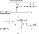
- a first electrode of the OLED is connected to the driving transistor Tdriver, a second electrode of the OLED is connected to the ground ELVSS, and the compensation circuit includes:
- both the transistor T20 and the transistor T30 are turned off, both the transistor T10 and the transistor Tdriver are turned on, and the data signal Vdata is written to the node N10 by the transistor T10.
Landscapes
- Engineering & Computer Science (AREA)
- Physics & Mathematics (AREA)
- Computer Hardware Design (AREA)
- General Physics & Mathematics (AREA)
- Theoretical Computer Science (AREA)
- Control Of El Displays (AREA)
- Control Of Indicators Other Than Cathode Ray Tubes (AREA)
- Electroluminescent Light Sources (AREA)
Applications Claiming Priority (2)
| Application Number | Priority Date | Filing Date | Title |
|---|---|---|---|
| CN201510232424.5A CN104778925B (zh) | 2015-05-08 | 2015-05-08 | Oled像素电路、显示装置及控制方法 |
| PCT/CN2015/092198 WO2016179962A1 (fr) | 2015-05-08 | 2015-10-19 | Circuit de pixels oled, dispositif d'affichage et procédé de commande |
Publications (3)
| Publication Number | Publication Date |
|---|---|
| EP3296983A1 true EP3296983A1 (fr) | 2018-03-21 |
| EP3296983A4 EP3296983A4 (fr) | 2018-12-12 |
| EP3296983B1 EP3296983B1 (fr) | 2020-09-16 |
Family
ID=53620356
Family Applications (1)
| Application Number | Title | Priority Date | Filing Date |
|---|---|---|---|
| EP15851606.2A Active EP3296983B1 (fr) | 2015-05-08 | 2015-10-19 | Circuit de pixels oled, dispositif d'affichage et procédé de commande |
Country Status (4)
| Country | Link |
|---|---|
| US (1) | US10210805B2 (fr) |
| EP (1) | EP3296983B1 (fr) |
| CN (1) | CN104778925B (fr) |
| WO (1) | WO2016179962A1 (fr) |
Families Citing this family (32)
| Publication number | Priority date | Publication date | Assignee | Title |
|---|---|---|---|---|
| CN104778925B (zh) * | 2015-05-08 | 2019-01-01 | 京东方科技集团股份有限公司 | Oled像素电路、显示装置及控制方法 |
| CN105702207B (zh) * | 2016-04-15 | 2019-01-18 | 京东方科技集团股份有限公司 | 防止关机时显示面板的画面残影的驱动方法及显示装置 |
| CN106097944B (zh) | 2016-08-11 | 2019-10-29 | 上海天马有机发光显示技术有限公司 | 一种显示面板和显示面板的阈值侦测方法 |
| TWI601279B (zh) * | 2016-08-22 | 2017-10-01 | 群創光電股份有限公司 | 發光二極體觸控顯示裝置 |
| CN106205489A (zh) * | 2016-09-30 | 2016-12-07 | 昆山国显光电有限公司 | 有机发光显示器及其驱动方法 |
| CN106782329B (zh) * | 2016-12-02 | 2019-09-10 | 上海天马微电子有限公司 | 一种有机发光显示面板及其驱动方法 |
| US10877276B1 (en) * | 2017-07-12 | 2020-12-29 | Facebook Technologies, Llc | Pixel design for calibration compensation |
| CN107393475A (zh) | 2017-08-10 | 2017-11-24 | 京东方科技集团股份有限公司 | 像素驱动电路、像素驱动方法和显示装置 |
| CN107424560B (zh) * | 2017-08-24 | 2020-03-13 | 京东方科技集团股份有限公司 | 显示面板中驱动晶体管阈值电压的检测方法及装置 |
| CN108062932B (zh) | 2017-12-20 | 2020-05-26 | 北京航空航天大学 | 一种有机薄膜晶体管构造的像素电路 |
| TWI639149B (zh) * | 2018-03-09 | 2018-10-21 | 友達光電股份有限公司 | 畫素電路 |
| US10586500B2 (en) * | 2018-04-27 | 2020-03-10 | Shenzhen China Star Optoelectronics Semiconductor Display Technology Co., Ltd. | Multiplexed type driver circuit, driving method and display |
| CN108288453B (zh) * | 2018-04-28 | 2023-04-07 | 京东方科技集团股份有限公司 | 一种像素电路及其驱动方法、显示面板和显示装置 |
| CN110858297B (zh) | 2018-08-24 | 2023-10-24 | 华为技术有限公司 | 光学指纹识别电路 |
| KR102631739B1 (ko) | 2018-11-29 | 2024-01-30 | 엘지디스플레이 주식회사 | 서브화소 구동 회로 및 이를 포함한 전계발광 표시장치 |
| CN109637450A (zh) * | 2019-01-09 | 2019-04-16 | 合肥京东方显示技术有限公司 | 像素驱动电路及其驱动方法、显示装置 |
| CN109817163A (zh) * | 2019-03-18 | 2019-05-28 | 合肥京东方光电科技有限公司 | 像素驱动电路和显示面板及其驱动方法、显示装置 |
| CN110264957B (zh) * | 2019-06-24 | 2021-01-26 | 京东方科技集团股份有限公司 | 一种像素电路的补偿方法、装置、显示设备 |
| CN110444161A (zh) * | 2019-06-28 | 2019-11-12 | 福建华佳彩有限公司 | 一种内部补偿电路 |
| TWI703548B (zh) * | 2019-07-24 | 2020-09-01 | 友達光電股份有限公司 | 畫素補償電路 |
| KR102753258B1 (ko) * | 2019-08-30 | 2025-01-15 | 삼성디스플레이 주식회사 | 표시장치 구동 방법 |
| CN111179864B (zh) * | 2020-01-16 | 2023-04-21 | Oppo广东移动通信有限公司 | 像素驱动电路及其驱动方法、显示装置、电子设备 |
| CN114067722A (zh) * | 2020-08-06 | 2022-02-18 | 深圳市柔宇科技股份有限公司 | 像素驱动电路、显示面板及像素驱动方法 |
| CN112951164A (zh) * | 2021-03-31 | 2021-06-11 | 深圳市华星光电半导体显示技术有限公司 | 像素驱动电路、显示面板及显示装置 |
| CN114743516B (zh) * | 2022-04-11 | 2023-10-20 | 惠科股份有限公司 | 补偿电路及液晶显示设备 |
| US11568813B1 (en) * | 2022-05-10 | 2023-01-31 | Meta Platforms Technologies, Llc | Pixel level burn-in compensation for light-emitting diode based displays |
| CN117456913A (zh) * | 2022-07-13 | 2024-01-26 | 北京京东方技术开发有限公司 | 半导体基板及其驱动方法、半导体显示装置 |
| KR20240009793A (ko) * | 2022-07-14 | 2024-01-23 | 엘지디스플레이 주식회사 | 표시 장치 및 그것의 화소 구동 방법 |
| CN115512657B (zh) * | 2022-11-23 | 2023-02-28 | 惠科股份有限公司 | 像素驱动电路及其驱动方法、显示面板 |
| TWI847772B (zh) * | 2023-06-20 | 2024-07-01 | 大陸商集創北方(珠海)科技有限公司 | 畫素電路、oled顯示裝置及資訊處理裝置 |
| KR20250004433A (ko) * | 2023-06-29 | 2025-01-08 | 삼성디스플레이 주식회사 | 화소 및 그것을 포함하는 표시 장치 |
| KR20250176187A (ko) | 2024-06-11 | 2025-12-19 | 삼성디스플레이 주식회사 | 화소 및 이를 구비하는 표시 장치 |
Family Cites Families (24)
| Publication number | Priority date | Publication date | Assignee | Title |
|---|---|---|---|---|
| JP2003216109A (ja) * | 2002-01-28 | 2003-07-30 | Sanyo Electric Co Ltd | 表示装置およびその表示の制御方法 |
| GB2411758A (en) * | 2004-03-04 | 2005-09-07 | Seiko Epson Corp | Pixel circuit |
| JP2005345992A (ja) | 2004-06-07 | 2005-12-15 | Chi Mei Electronics Corp | 表示装置 |
| TWI288377B (en) * | 2004-09-01 | 2007-10-11 | Au Optronics Corp | Organic light emitting display and display unit thereof |
| KR101152119B1 (ko) * | 2005-02-07 | 2012-06-15 | 삼성전자주식회사 | 표시 장치 및 그 구동 방법 |
| KR100624137B1 (ko) * | 2005-08-22 | 2006-09-13 | 삼성에스디아이 주식회사 | 유기 전계 발광 표시장치의 화소회로 및 그의 구동방법 |
| JP4530017B2 (ja) * | 2007-09-26 | 2010-08-25 | ソニー株式会社 | 表示装置、表示駆動方法 |
| US20090284515A1 (en) | 2008-05-16 | 2009-11-19 | Toshiba Matsushita Display Technology Co., Ltd. | El display device |
| JP2010224390A (ja) * | 2009-03-25 | 2010-10-07 | Seiko Epson Corp | 単位回路、並びに単位回路及び電気光学装置の駆動方法 |
| TWI417840B (zh) * | 2009-08-26 | 2013-12-01 | Au Optronics Corp | 畫素電路、主動式矩陣有機發光二極體顯示器及畫素電路之驅動方法 |
| JP2011069943A (ja) * | 2009-09-25 | 2011-04-07 | Sony Corp | 表示装置および電子機器 |
| KR101152575B1 (ko) * | 2010-05-10 | 2012-06-01 | 삼성모바일디스플레이주식회사 | 평판 표시 장치의 화소 회로 및 그의 구동 방법 |
| KR101818462B1 (ko) * | 2011-06-28 | 2018-01-16 | 엘지디스플레이 주식회사 | 유기전계발광 표시장치의 구동회로 및 구동방법 |
| CN103578405B (zh) * | 2012-07-19 | 2016-12-07 | 群康科技(深圳)有限公司 | 显示面板、像素驱动电路、驱动像素方法与电子装置 |
| TWI460706B (zh) * | 2012-10-11 | 2014-11-11 | Au Optronics Corp | 有機發光顯示器與其驅動電路以及驅動其之方法 |
| KR101970574B1 (ko) * | 2012-12-28 | 2019-08-27 | 엘지디스플레이 주식회사 | Oled 표시 장치 |
| CN105144274B (zh) * | 2013-04-23 | 2017-07-11 | 夏普株式会社 | 显示装置及其驱动电流检测方法 |
| US9123289B2 (en) * | 2013-06-26 | 2015-09-01 | Lg Display Co., Ltd. | Organic light emitting diode display device with reference voltage lines and method of operation in an organic light emitting diode display device |
| CN103440840B (zh) * | 2013-07-15 | 2015-09-16 | 北京大学深圳研究生院 | 一种显示装置及其像素电路 |
| CN103943067B (zh) * | 2014-03-31 | 2017-04-12 | 京东方科技集团股份有限公司 | 一种像素电路及其驱动方法、显示装置 |
| TWI517125B (zh) * | 2014-04-09 | 2016-01-11 | 友達光電股份有限公司 | 畫素驅動電路 |
| CN104064139B (zh) * | 2014-06-05 | 2016-06-29 | 上海天马有机发光显示技术有限公司 | 一种有机发光二极管像素补偿电路、显示面板和显示装置 |
| CN104299572B (zh) * | 2014-11-06 | 2016-10-12 | 京东方科技集团股份有限公司 | 像素电路、显示基板和显示面板 |
| CN104778925B (zh) * | 2015-05-08 | 2019-01-01 | 京东方科技集团股份有限公司 | Oled像素电路、显示装置及控制方法 |
-
2015
- 2015-05-08 CN CN201510232424.5A patent/CN104778925B/zh active Active
- 2015-10-19 EP EP15851606.2A patent/EP3296983B1/fr active Active
- 2015-10-19 WO PCT/CN2015/092198 patent/WO2016179962A1/fr not_active Ceased
- 2015-10-19 US US15/031,498 patent/US10210805B2/en active Active
Also Published As
| Publication number | Publication date |
|---|---|
| US20180197462A1 (en) | 2018-07-12 |
| EP3296983A4 (fr) | 2018-12-12 |
| US10210805B2 (en) | 2019-02-19 |
| EP3296983B1 (fr) | 2020-09-16 |
| WO2016179962A1 (fr) | 2016-11-17 |
| CN104778925A (zh) | 2015-07-15 |
| CN104778925B (zh) | 2019-01-01 |
Similar Documents
| Publication | Publication Date | Title |
|---|---|---|
| US10210805B2 (en) | Organic light-emitting diode (OLED) pixel circuit, display device and control method | |
| US10431153B2 (en) | Pixel circuit, method for driving the same, and organic electroluminescent display panel | |
| US10916184B2 (en) | Array substrate and driving method thereof, display panel, display device | |
| KR102783396B1 (ko) | 게이트 드라이버를 갖는 디스플레이 장치 | |
| US10665170B2 (en) | Display device | |
| EP3163562B1 (fr) | Circuit de pixel, écran d'affichage et dispositif d'affichage | |
| US20200027402A1 (en) | Pixel circuit, driving method, organic light emitting display panel, and display device | |
| CN111613177A (zh) | 一种像素电路及其驱动方法、显示面板和显示装置 | |
| EP3355298B1 (fr) | Circuit d'attaque de pixel, procédé, circuit de pixel et dispositif d'affichage | |
| EP3159879B1 (fr) | Circuit pour pixels et dispositif d'affichage | |
| WO2016095545A1 (fr) | Circuit de pixel et procédé d'attaque, panneau d'affichage et appareil d'affichage | |
| CN103946912B (zh) | 显示装置及其控制方法 | |
| EP3159878B1 (fr) | Circuit de pixels et dispositif d'affichage | |
| WO2020181515A1 (fr) | Circuit de pixels et son procédé d'attaque, et dispositif d'affichage | |
| TW201351378A (zh) | 顯示器 | |
| US20180005570A1 (en) | Pixel circuit, driving method for the pixel circuit, display panel, and display device | |
| US10235943B2 (en) | Display panel, method for controlling display panel and display device | |
| US11037508B1 (en) | Pixel driving circuit, display panel and methods for driving the same | |
| CN109935207B (zh) | 像素驱动电路、像素电路和显示装置及其驱动方法 | |
| US20180247592A1 (en) | Pixel Driving Circuit and Driving Method Thereof, Array Substrate, and Display Device | |
| JP6288710B2 (ja) | 表示装置の駆動方法および表示装置 | |
| US20210049964A1 (en) | Pixel circuit and method of controlling the same, display panel and display device | |
| US10140921B2 (en) | EM signal control circuit, EM signal control method and organic light emitting display device | |
| KR20180024376A (ko) | 유기발광표시장치 | |
| KR20170003284A (ko) | 컨트롤러, 유기발광표시패널, 유기발광표시장치 및 그 구동 방법 |
Legal Events
| Date | Code | Title | Description |
|---|---|---|---|
| STAA | Information on the status of an ep patent application or granted ep patent |
Free format text: STATUS: THE INTERNATIONAL PUBLICATION HAS BEEN MADE |
|
| PUAI | Public reference made under article 153(3) epc to a published international application that has entered the european phase |
Free format text: ORIGINAL CODE: 0009012 |
|
| STAA | Information on the status of an ep patent application or granted ep patent |
Free format text: STATUS: REQUEST FOR EXAMINATION WAS MADE |
|
| 17P | Request for examination filed |
Effective date: 20160422 |
|
| AK | Designated contracting states |
Kind code of ref document: A1 Designated state(s): AL AT BE BG CH CY CZ DE DK EE ES FI FR GB GR HR HU IE IS IT LI LT LU LV MC MK MT NL NO PL PT RO RS SE SI SK SM TR |
|
| AX | Request for extension of the european patent |
Extension state: BA ME |
|
| DAV | Request for validation of the european patent (deleted) | ||
| DAX | Request for extension of the european patent (deleted) | ||
| A4 | Supplementary search report drawn up and despatched |
Effective date: 20181107 |
|
| RIC1 | Information provided on ipc code assigned before grant |
Ipc: G09G 3/3291 20160101ALI20181102BHEP Ipc: G09G 3/32 20160101AFI20181102BHEP |
|
| GRAP | Despatch of communication of intention to grant a patent |
Free format text: ORIGINAL CODE: EPIDOSNIGR1 |
|
| STAA | Information on the status of an ep patent application or granted ep patent |
Free format text: STATUS: GRANT OF PATENT IS INTENDED |
|
| INTG | Intention to grant announced |
Effective date: 20200428 |
|
| GRAS | Grant fee paid |
Free format text: ORIGINAL CODE: EPIDOSNIGR3 |
|
| GRAA | (expected) grant |
Free format text: ORIGINAL CODE: 0009210 |
|
| STAA | Information on the status of an ep patent application or granted ep patent |
Free format text: STATUS: THE PATENT HAS BEEN GRANTED |
|
| AK | Designated contracting states |
Kind code of ref document: B1 Designated state(s): AL AT BE BG CH CY CZ DE DK EE ES FI FR GB GR HR HU IE IS IT LI LT LU LV MC MK MT NL NO PL PT RO RS SE SI SK SM TR |
|
| REG | Reference to a national code |
Ref country code: GB Ref legal event code: FG4D |
|
| REG | Reference to a national code |
Ref country code: CH Ref legal event code: EP |
|
| REG | Reference to a national code |
Ref country code: DE Ref legal event code: R096 Ref document number: 602015059308 Country of ref document: DE |
|
| REG | Reference to a national code |
Ref country code: IE Ref legal event code: FG4D |
|
| REG | Reference to a national code |
Ref country code: AT Ref legal event code: REF Ref document number: 1314853 Country of ref document: AT Kind code of ref document: T Effective date: 20201015 |
|
| PG25 | Lapsed in a contracting state [announced via postgrant information from national office to epo] |
Ref country code: FI Free format text: LAPSE BECAUSE OF FAILURE TO SUBMIT A TRANSLATION OF THE DESCRIPTION OR TO PAY THE FEE WITHIN THE PRESCRIBED TIME-LIMIT Effective date: 20200916 Ref country code: GR Free format text: LAPSE BECAUSE OF FAILURE TO SUBMIT A TRANSLATION OF THE DESCRIPTION OR TO PAY THE FEE WITHIN THE PRESCRIBED TIME-LIMIT Effective date: 20201217 Ref country code: NO Free format text: LAPSE BECAUSE OF FAILURE TO SUBMIT A TRANSLATION OF THE DESCRIPTION OR TO PAY THE FEE WITHIN THE PRESCRIBED TIME-LIMIT Effective date: 20201216 Ref country code: SE Free format text: LAPSE BECAUSE OF FAILURE TO SUBMIT A TRANSLATION OF THE DESCRIPTION OR TO PAY THE FEE WITHIN THE PRESCRIBED TIME-LIMIT Effective date: 20200916 Ref country code: BG Free format text: LAPSE BECAUSE OF FAILURE TO SUBMIT A TRANSLATION OF THE DESCRIPTION OR TO PAY THE FEE WITHIN THE PRESCRIBED TIME-LIMIT Effective date: 20201216 Ref country code: HR Free format text: LAPSE BECAUSE OF FAILURE TO SUBMIT A TRANSLATION OF THE DESCRIPTION OR TO PAY THE FEE WITHIN THE PRESCRIBED TIME-LIMIT Effective date: 20200916 |
|
| REG | Reference to a national code |
Ref country code: AT Ref legal event code: MK05 Ref document number: 1314853 Country of ref document: AT Kind code of ref document: T Effective date: 20200916 |
|
| REG | Reference to a national code |
Ref country code: NL Ref legal event code: MP Effective date: 20200916 |
|
| PG25 | Lapsed in a contracting state [announced via postgrant information from national office to epo] |
Ref country code: LV Free format text: LAPSE BECAUSE OF FAILURE TO SUBMIT A TRANSLATION OF THE DESCRIPTION OR TO PAY THE FEE WITHIN THE PRESCRIBED TIME-LIMIT Effective date: 20200916 Ref country code: RS Free format text: LAPSE BECAUSE OF FAILURE TO SUBMIT A TRANSLATION OF THE DESCRIPTION OR TO PAY THE FEE WITHIN THE PRESCRIBED TIME-LIMIT Effective date: 20200916 |
|
| REG | Reference to a national code |
Ref country code: LT Ref legal event code: MG4D |
|
| PG25 | Lapsed in a contracting state [announced via postgrant information from national office to epo] |
Ref country code: RO Free format text: LAPSE BECAUSE OF FAILURE TO SUBMIT A TRANSLATION OF THE DESCRIPTION OR TO PAY THE FEE WITHIN THE PRESCRIBED TIME-LIMIT Effective date: 20200916 Ref country code: PT Free format text: LAPSE BECAUSE OF FAILURE TO SUBMIT A TRANSLATION OF THE DESCRIPTION OR TO PAY THE FEE WITHIN THE PRESCRIBED TIME-LIMIT Effective date: 20210118 Ref country code: SM Free format text: LAPSE BECAUSE OF FAILURE TO SUBMIT A TRANSLATION OF THE DESCRIPTION OR TO PAY THE FEE WITHIN THE PRESCRIBED TIME-LIMIT Effective date: 20200916 Ref country code: EE Free format text: LAPSE BECAUSE OF FAILURE TO SUBMIT A TRANSLATION OF THE DESCRIPTION OR TO PAY THE FEE WITHIN THE PRESCRIBED TIME-LIMIT Effective date: 20200916 Ref country code: LT Free format text: LAPSE BECAUSE OF FAILURE TO SUBMIT A TRANSLATION OF THE DESCRIPTION OR TO PAY THE FEE WITHIN THE PRESCRIBED TIME-LIMIT Effective date: 20200916 Ref country code: CZ Free format text: LAPSE BECAUSE OF FAILURE TO SUBMIT A TRANSLATION OF THE DESCRIPTION OR TO PAY THE FEE WITHIN THE PRESCRIBED TIME-LIMIT Effective date: 20200916 |
|
| PG25 | Lapsed in a contracting state [announced via postgrant information from national office to epo] |
Ref country code: PL Free format text: LAPSE BECAUSE OF FAILURE TO SUBMIT A TRANSLATION OF THE DESCRIPTION OR TO PAY THE FEE WITHIN THE PRESCRIBED TIME-LIMIT Effective date: 20200916 Ref country code: IS Free format text: LAPSE BECAUSE OF FAILURE TO SUBMIT A TRANSLATION OF THE DESCRIPTION OR TO PAY THE FEE WITHIN THE PRESCRIBED TIME-LIMIT Effective date: 20210116 Ref country code: AL Free format text: LAPSE BECAUSE OF FAILURE TO SUBMIT A TRANSLATION OF THE DESCRIPTION OR TO PAY THE FEE WITHIN THE PRESCRIBED TIME-LIMIT Effective date: 20200916 Ref country code: AT Free format text: LAPSE BECAUSE OF FAILURE TO SUBMIT A TRANSLATION OF THE DESCRIPTION OR TO PAY THE FEE WITHIN THE PRESCRIBED TIME-LIMIT Effective date: 20200916 Ref country code: ES Free format text: LAPSE BECAUSE OF FAILURE TO SUBMIT A TRANSLATION OF THE DESCRIPTION OR TO PAY THE FEE WITHIN THE PRESCRIBED TIME-LIMIT Effective date: 20200916 |
|
| REG | Reference to a national code |
Ref country code: CH Ref legal event code: PL |
|
| REG | Reference to a national code |
Ref country code: DE Ref legal event code: R097 Ref document number: 602015059308 Country of ref document: DE |
|
| PG25 | Lapsed in a contracting state [announced via postgrant information from national office to epo] |
Ref country code: SK Free format text: LAPSE BECAUSE OF FAILURE TO SUBMIT A TRANSLATION OF THE DESCRIPTION OR TO PAY THE FEE WITHIN THE PRESCRIBED TIME-LIMIT Effective date: 20200916 Ref country code: LU Free format text: LAPSE BECAUSE OF NON-PAYMENT OF DUE FEES Effective date: 20201019 Ref country code: MC Free format text: LAPSE BECAUSE OF FAILURE TO SUBMIT A TRANSLATION OF THE DESCRIPTION OR TO PAY THE FEE WITHIN THE PRESCRIBED TIME-LIMIT Effective date: 20200916 |
|
| REG | Reference to a national code |
Ref country code: BE Ref legal event code: MM Effective date: 20201031 |
|
| PLBE | No opposition filed within time limit |
Free format text: ORIGINAL CODE: 0009261 |
|
| STAA | Information on the status of an ep patent application or granted ep patent |
Free format text: STATUS: NO OPPOSITION FILED WITHIN TIME LIMIT |
|
| 26N | No opposition filed |
Effective date: 20210617 |
|
| GBPC | Gb: european patent ceased through non-payment of renewal fee |
Effective date: 20201216 |
|
| PG25 | Lapsed in a contracting state [announced via postgrant information from national office to epo] |
Ref country code: LI Free format text: LAPSE BECAUSE OF NON-PAYMENT OF DUE FEES Effective date: 20201031 Ref country code: SI Free format text: LAPSE BECAUSE OF FAILURE TO SUBMIT A TRANSLATION OF THE DESCRIPTION OR TO PAY THE FEE WITHIN THE PRESCRIBED TIME-LIMIT Effective date: 20200916 Ref country code: BE Free format text: LAPSE BECAUSE OF NON-PAYMENT OF DUE FEES Effective date: 20201031 Ref country code: DK Free format text: LAPSE BECAUSE OF FAILURE TO SUBMIT A TRANSLATION OF THE DESCRIPTION OR TO PAY THE FEE WITHIN THE PRESCRIBED TIME-LIMIT Effective date: 20200916 Ref country code: CH Free format text: LAPSE BECAUSE OF NON-PAYMENT OF DUE FEES Effective date: 20201031 |
|
| PG25 | Lapsed in a contracting state [announced via postgrant information from national office to epo] |
Ref country code: FR Free format text: LAPSE BECAUSE OF NON-PAYMENT OF DUE FEES Effective date: 20201116 Ref country code: IE Free format text: LAPSE BECAUSE OF NON-PAYMENT OF DUE FEES Effective date: 20201019 Ref country code: IT Free format text: LAPSE BECAUSE OF FAILURE TO SUBMIT A TRANSLATION OF THE DESCRIPTION OR TO PAY THE FEE WITHIN THE PRESCRIBED TIME-LIMIT Effective date: 20200916 |
|
| PG25 | Lapsed in a contracting state [announced via postgrant information from national office to epo] |
Ref country code: GB Free format text: LAPSE BECAUSE OF NON-PAYMENT OF DUE FEES Effective date: 20201216 |
|
| PG25 | Lapsed in a contracting state [announced via postgrant information from national office to epo] |
Ref country code: IS Free format text: LAPSE BECAUSE OF FAILURE TO SUBMIT A TRANSLATION OF THE DESCRIPTION OR TO PAY THE FEE WITHIN THE PRESCRIBED TIME-LIMIT Effective date: 20210116 Ref country code: TR Free format text: LAPSE BECAUSE OF FAILURE TO SUBMIT A TRANSLATION OF THE DESCRIPTION OR TO PAY THE FEE WITHIN THE PRESCRIBED TIME-LIMIT Effective date: 20200916 Ref country code: MT Free format text: LAPSE BECAUSE OF FAILURE TO SUBMIT A TRANSLATION OF THE DESCRIPTION OR TO PAY THE FEE WITHIN THE PRESCRIBED TIME-LIMIT Effective date: 20200916 Ref country code: CY Free format text: LAPSE BECAUSE OF FAILURE TO SUBMIT A TRANSLATION OF THE DESCRIPTION OR TO PAY THE FEE WITHIN THE PRESCRIBED TIME-LIMIT Effective date: 20200916 |
|
| PG25 | Lapsed in a contracting state [announced via postgrant information from national office to epo] |
Ref country code: MK Free format text: LAPSE BECAUSE OF FAILURE TO SUBMIT A TRANSLATION OF THE DESCRIPTION OR TO PAY THE FEE WITHIN THE PRESCRIBED TIME-LIMIT Effective date: 20200916 |
|
| PG25 | Lapsed in a contracting state [announced via postgrant information from national office to epo] |
Ref country code: NL Free format text: LAPSE BECAUSE OF NON-PAYMENT OF DUE FEES Effective date: 20200923 |
|
| PGFP | Annual fee paid to national office [announced via postgrant information from national office to epo] |
Ref country code: DE Payment date: 20251020 Year of fee payment: 11 |