EP3298446B1 - Procédé de mesure et ensemble de mesure pour un système optique de formation d'image - Google Patents
Procédé de mesure et ensemble de mesure pour un système optique de formation d'image Download PDFInfo
- Publication number
- EP3298446B1 EP3298446B1 EP16727302.8A EP16727302A EP3298446B1 EP 3298446 B1 EP3298446 B1 EP 3298446B1 EP 16727302 A EP16727302 A EP 16727302A EP 3298446 B1 EP3298446 B1 EP 3298446B1
- Authority
- EP
- European Patent Office
- Prior art keywords
- optical
- arrangement
- measurement
- measuring
- measured
- Prior art date
- Legal status (The legal status is an assumption and is not a legal conclusion. Google has not performed a legal analysis and makes no representation as to the accuracy of the status listed.)
- Active
Links
Images





Classifications
-
- G—PHYSICS
- G01—MEASURING; TESTING
- G01B—MEASURING LENGTH, THICKNESS OR SIMILAR LINEAR DIMENSIONS; MEASURING ANGLES; MEASURING AREAS; MEASURING IRREGULARITIES OF SURFACES OR CONTOURS
- G01B9/00—Measuring instruments characterised by the use of optical techniques
- G01B9/02—Interferometers
- G01B9/02034—Interferometers characterised by particularly shaped beams or wavefronts
-
- G—PHYSICS
- G01—MEASURING; TESTING
- G01B—MEASURING LENGTH, THICKNESS OR SIMILAR LINEAR DIMENSIONS; MEASURING ANGLES; MEASURING AREAS; MEASURING IRREGULARITIES OF SURFACES OR CONTOURS
- G01B11/00—Measuring arrangements characterised by the use of optical techniques
- G01B11/24—Measuring arrangements characterised by the use of optical techniques for measuring contours or curvatures
-
- G—PHYSICS
- G01—MEASURING; TESTING
- G01M—TESTING STATIC OR DYNAMIC BALANCE OF MACHINES OR STRUCTURES; TESTING OF STRUCTURES OR APPARATUS, NOT OTHERWISE PROVIDED FOR
- G01M11/00—Testing of optical apparatus; Testing structures by optical methods not otherwise provided for
- G01M11/02—Testing optical properties
- G01M11/0242—Testing optical properties by measuring geometrical properties or aberrations
- G01M11/0257—Testing optical properties by measuring geometrical properties or aberrations by analyzing the image formed by the object to be tested
-
- G—PHYSICS
- G01—MEASURING; TESTING
- G01M—TESTING STATIC OR DYNAMIC BALANCE OF MACHINES OR STRUCTURES; TESTING OF STRUCTURES OR APPARATUS, NOT OTHERWISE PROVIDED FOR
- G01M11/00—Testing of optical apparatus; Testing structures by optical methods not otherwise provided for
- G01M11/02—Testing optical properties
- G01M11/0242—Testing optical properties by measuring geometrical properties or aberrations
- G01M11/0257—Testing optical properties by measuring geometrical properties or aberrations by analyzing the image formed by the object to be tested
- G01M11/0264—Testing optical properties by measuring geometrical properties or aberrations by analyzing the image formed by the object to be tested by using targets or reference patterns
-
- G—PHYSICS
- G03—PHOTOGRAPHY; CINEMATOGRAPHY; ANALOGOUS TECHNIQUES USING WAVES OTHER THAN OPTICAL WAVES; ELECTROGRAPHY; HOLOGRAPHY
- G03F—PHOTOMECHANICAL PRODUCTION OF TEXTURED OR PATTERNED SURFACES, e.g. FOR PRINTING, FOR PROCESSING OF SEMICONDUCTOR DEVICES; MATERIALS THEREFOR; ORIGINALS THEREFOR; APPARATUS SPECIALLY ADAPTED THEREFOR
- G03F7/00—Photomechanical, e.g. photolithographic, production of textured or patterned surfaces, e.g. printing surfaces; Materials therefor, e.g. comprising photoresists; Apparatus specially adapted therefor
- G03F7/70—Microphotolithographic exposure; Apparatus therefor
- G03F7/70216—Mask projection systems
- G03F7/70258—Projection system adjustments, e.g. adjustments during exposure or alignment during assembly of projection system
-
- G—PHYSICS
- G03—PHOTOGRAPHY; CINEMATOGRAPHY; ANALOGOUS TECHNIQUES USING WAVES OTHER THAN OPTICAL WAVES; ELECTROGRAPHY; HOLOGRAPHY
- G03F—PHOTOMECHANICAL PRODUCTION OF TEXTURED OR PATTERNED SURFACES, e.g. FOR PRINTING, FOR PROCESSING OF SEMICONDUCTOR DEVICES; MATERIALS THEREFOR; ORIGINALS THEREFOR; APPARATUS SPECIALLY ADAPTED THEREFOR
- G03F7/00—Photomechanical, e.g. photolithographic, production of textured or patterned surfaces, e.g. printing surfaces; Materials therefor, e.g. comprising photoresists; Apparatus specially adapted therefor
- G03F7/70—Microphotolithographic exposure; Apparatus therefor
- G03F7/70483—Information management; Active and passive control; Testing; Wafer monitoring, e.g. pattern monitoring
- G03F7/70491—Information management, e.g. software; Active and passive control, e.g. details of controlling exposure processes or exposure tool monitoring processes
- G03F7/70516—Calibration of components of the microlithographic apparatus, e.g. light sources, addressable masks or detectors
-
- G—PHYSICS
- G03—PHOTOGRAPHY; CINEMATOGRAPHY; ANALOGOUS TECHNIQUES USING WAVES OTHER THAN OPTICAL WAVES; ELECTROGRAPHY; HOLOGRAPHY
- G03F—PHOTOMECHANICAL PRODUCTION OF TEXTURED OR PATTERNED SURFACES, e.g. FOR PRINTING, FOR PROCESSING OF SEMICONDUCTOR DEVICES; MATERIALS THEREFOR; ORIGINALS THEREFOR; APPARATUS SPECIALLY ADAPTED THEREFOR
- G03F7/00—Photomechanical, e.g. photolithographic, production of textured or patterned surfaces, e.g. printing surfaces; Materials therefor, e.g. comprising photoresists; Apparatus specially adapted therefor
- G03F7/70—Microphotolithographic exposure; Apparatus therefor
- G03F7/70483—Information management; Active and passive control; Testing; Wafer monitoring, e.g. pattern monitoring
- G03F7/70591—Testing optical components
- G03F7/706—Aberration measurement
-
- G—PHYSICS
- G03—PHOTOGRAPHY; CINEMATOGRAPHY; ANALOGOUS TECHNIQUES USING WAVES OTHER THAN OPTICAL WAVES; ELECTROGRAPHY; HOLOGRAPHY
- G03F—PHOTOMECHANICAL PRODUCTION OF TEXTURED OR PATTERNED SURFACES, e.g. FOR PRINTING, FOR PROCESSING OF SEMICONDUCTOR DEVICES; MATERIALS THEREFOR; ORIGINALS THEREFOR; APPARATUS SPECIALLY ADAPTED THEREFOR
- G03F7/00—Photomechanical, e.g. photolithographic, production of textured or patterned surfaces, e.g. printing surfaces; Materials therefor, e.g. comprising photoresists; Apparatus specially adapted therefor
- G03F7/70—Microphotolithographic exposure; Apparatus therefor
- G03F7/708—Construction of apparatus, e.g. environment aspects, hygiene aspects or materials
- G03F7/7085—Detection arrangement, e.g. detectors of apparatus alignment possibly mounted on wafers, exposure dose, photo-cleaning flux, stray light, thermal load
Definitions
- the invention relates to a measuring arrangement for measuring an optical unit of a projection exposure system for microlithography. Furthermore, the invention relates to a measuring device and a method for interferometric shape measurement of optical surfaces. Furthermore, the invention relates to a method for measuring a wavefront error of an imaging optical system of a projection exposure system.
- the imaging optical system comprises a plurality of optical elements for imaging a pattern from an object plane into an image plane.
- a projection exposure system is used in microlithography to expose a photosensitive material on a wafer with an image of structures on a mask or reticle.
- the projection exposure system usually contains an illumination system and a projection lens.
- the illumination system generates a desired radiation distribution for illuminating the structures of the mask, while the projection lens images the illuminated structures with very high resolution onto the photosensitive material of the wafer.
- the optical elements used in the projection exposure system must be manufactured and positioned with extremely high precision. For this purpose, During the manufacture or readjustment of projection exposure systems, both a measurement of a complete imaging optical system and of individual optical elements can be carried out.
- phase-shifting interferometry techniques such as shearing interferometry or point diffraction interferometry are used.
- DE 103 16 123 A1 Such a device for wavefront measurement of a projection lens for microlithography by shear interferometry is described.
- diffractive optical arrangements For precise shape measurement of the surface of an optical element, diffractive optical arrangements, known as null optics, are often used as interferometric measuring devices.
- the wavefront of a test wave is adapted to a desired surface shape by a diffractive element, such as a computer-generated hologram (CGH). Deviations from the desired shape can be determined by superimposing the test wave reflected by the optical element with a reference wave.
- a measuring device is used, for example, in DE 10 2012 217 800 A1 described.
- the object is achieved by the following measuring arrangement for measuring an optical unit of a projection exposure system for microlithography.
- the measuring device contains a wavefront measuring device configured to measure a wavefront error of an imaging optics using a measuring radiation.
- the measuring arrangement contains at least one adaptation module configured to manipulate the wavefront of the measuring radiation such that the combination of the optical unit to be measured and the at least one adaptation module forms an imaging optical arrangement.
- the optical unit can in particular be one of the sub-arrangements described below within the scope of a measuring method according to the invention and thus a sub-arrangement of an imaging optical system of a projection exposure system, such as an optical module of a projection objective of the projection exposure system.
- the projection exposure system can be an EUV projection exposure system.
- the optical unit to be measured is configured as a non-imaging optical system which, upon irradiation with a plane or spherical input wave having a wavelength ⁇ , generates an output wave whose wavefront deviates from an ideal spherical wave at at least one point by at least ⁇ , in particular at least 10 ⁇ .
- a non-imaging optical system which, upon irradiation with a plane or spherical input wave having a wavelength ⁇ , generates an output wave whose wavefront deviates from an ideal spherical wave at at least one point by at least ⁇ , in particular at least 10 ⁇ .
- An imaging optical arrangement is also referred to in this description as an optical arrangement which, upon irradiation with a plane or spherical input wave having a wavelength ⁇ , generates an output wave whose wavefront deviates from an ideal spherical wave at no point by more than ⁇ , in particular at no point by more than 10 ⁇ .
- the measuring arrangement it is configured to measure the optical unit in the form of a non-imaging optic which, upon irradiation of a plane or a spherical input wave with a wavelength ⁇ , generates an output wave whose wavefront deviates at least ⁇ from an ideal spherical wave at at least one point.
- the optical unit is assigned to an imaging optical system comprising a plurality of optical elements of a projection exposure apparatus for microlithography, and the optical unit is formed by one of the optical elements of the imaging optical system or by a partial arrangement of the optical elements of the imaging optical system.
- a partial arrangement of the optical elements is to be understood as an arrangement of optical elements, i.e.
- an imaging optical system of the projection exposure apparatus comprises a plurality of optical modules, each comprising at least two optical elements, and the optical arrangement comprises at least one of the optical modules and fewer than the plurality of optical modules.
- the optical unit is formed by a partial arrangement of the optical elements of the imaging optical system, wherein the partial arrangement of the optical elements differs from at least one section of the imaging optical system by the presence of a gap relating to at least one optical element.
- the adaptation module is configured to shorten a back focal length of the optical unit to be measured.
- the optical unit to be measured already forms an imaging optical system, but with an unwieldy large back focal length. This can be the lens-side and/or the image-side back focal length.
- the optical unit is an imaging optical system, in particular a projection lens of a projection exposure system for microlithography, but with a large back focal length.
- the arrangement comprising the optical unit and the adaptation module forms an imaging optical arrangement with a back focal length that is shorter than that of the optical unit.
- the measuring arrangement further comprises a calibration unit having the optical function of the optical unit to be measured, which is configured to calibrate the at least one adaptation module by determining a wavefront error of an arrangement comprising the at least one adaptation module and the calibration unit prior to the measurement of the optical unit.
- the calibration unit can comprise one or more calibration modules.
- the calibration unit can A first calibration module having the function of the section of the optical unit arranged in front of the gap, and a second calibration module having the function of the section of the optical unit arranged after the gap.
- the calibration unit comprises one or more diffractive structural patterns for manipulating the measuring radiation.
- the wavefront measuring device and the adaptation module of the measuring arrangement can be designed according to the embodiment variants of a wavefront measuring device or an adaptation module described below with reference to the method for measuring a wavefront error according to the first aspect of the invention.
- the measuring arrangement according to the invention and the measuring method according to the invention enable separate measurement of individual optical modules of an imaging optical system, even in cases where the optical modules are not imaging optics. This enables the cause of a wavefront error in the imaging optical system to be determined with high accuracy and with less time expenditure compared to an individual measurement of any optical elements contained in the optical module. Furthermore, the separate measurement of individual optical modules enables the cause of a wavefront error to be determined prior to the measurement of the entire imaging optical system.
- the at least one adaptation module comprises an input-side adaptation module for manipulating the measuring radiation, which is arranged in a beam path of the measuring radiation upstream of the optical unit to be measured, and an output-side adaptation module for manipulating the measuring radiation, which is arranged in the beam path of the measuring radiation downstream of the optical unit to be measured.
- Both adaptation modules contain at least one optical element.
- the optical elements of the adaptation modules are designed and arranged, for example, such that, together with the optical unit to be measured, they form an imaging optical arrangement.
- the adaptation modules are configured such that the optical arrangement corresponds in its optical effect to an imaging optical system to be measured, wherein the optical unit is one of several optical modules of the optical system to be measured.
- the optical arrangement can also have other imaging properties, in particular a different focal length or a different imaging scale.
- the at least one adaptation module has one or more diffractive structure patterns used in reflection or transmission.
- the at least one adaptation module contains one or more CGHs with diffractive structure patterns.
- at least one CGH is provided in the beam path of the wavefront measuring device before or after the module to be measured, or in each of both adaptation modules.
- two or more successively arranged diffractive structure patterns, such as CGHs each with a diffractive structure can also be operated in reflection.
- the at least one adaptation module contains at least two diffractive structure patterns arranged superimposed on one another or one behind the other in a beam path of the measuring radiation.
- the diffractive structure patterns arranged one behind the other are each own substrate, as is the case in the US 2012/ 0127481 A1
- two or more CGHs arranged one behind the other in the beam path are used.
- the two superimposed structural patterns are arranged on a single substrate in the same plane, as is shown, for example, in the DE 10 2012 217 800 A1
- at least one complex-encoded CGH with two or more superimposed diffractive structure patterns can be provided in the adaptation module.
- the object is achieved by the method described below for measuring a wavefront error of an imaging optical system of a projection exposure system for microlithography.
- the optical system contains a plurality of optical elements for imaging a pattern from an object plane into an image plane.
- the method comprises a separate measurement of respective wavefront errors of different subarrangements of the optical elements.
- the cause of a wavefront error in the imaging optical system can be narrowed down to one of the sub-arrays.
- the next step can then be, for example, a measurement of the individual optical elements of this sub-array.
- a single optical element can be identified as the source of the error from the measurement results of the sub-arrays. Individual measurement of all optical In any case, it is not necessary to measure the elements of the imaging optical system. This minimizes the time required to determine the cause of a wavefront error in the imaging optical system without compromising accuracy.
- one of the partial arrangements of the optical elements differs from at least one section of the imaging optical system by the presence of a gap relating to at least one optical element.
- a gap in the arrangement is characterized in that, in the beam path of the imaging optical system, at least one optical element is positioned upstream of the gap and at least one optical element is positioned downstream of the gap.
- the imaging optical system is provided with a plurality of optical modules, each comprising at least two of the optical elements, and the separate measurement of the respective wavefront errors of different sub-arrangements is carried out by separately measuring the respective wavefront errors of the individual optical modules.
- the different sub-arrangements are formed by the optical modules.
- the imaging optical system is divided into a plurality of modules.
- Each of the modules comprises at least two optical elements, preferably arranged one after the other in the beam path of the optical system.
- each optical module can be removed from the optical system as a whole and inserted back into it.
- adjustment means are provided for adjusting one or more modules in the optical system.
- the imaging optical system is a projection lens of a projection exposure system for microlithography.
- the imaging optical system can also be another imaging optical assembly from the exposure beam path of the projection exposure system, such as an imaging optical assembly of an illumination system of the projection exposure system.
- the imaging optical system can be at least a part of either a projection lens or an illumination system of a projection exposure system, i.e., either a part of the projection lens or the illumination system or the entire projection lens or the entire illumination system.
- at least one of the subassemblies is not an imaging optical system, but rather a non-stigmatic optical system, as defined above, or, for example, an optical system with a defocusing or beam-expanding effect.
- the subassemblies in the form of the optical modules of the imaging optical system are contained in a common housing during operation of the projection exposure system.
- the method according to the invention further comprises combining the measurement results for the individual sub-arrangements to form a result for the wavefront error of the entire imaging optical system.
- the wavefront error of the entire imaging optical system is thus measured by separately measuring the sub-arrangements and subsequently combining the measurement results to form an overall result.
- the modular design of the imaging optical system makes post-processing or adaptation significantly faster and more straightforward.
- the imaging optical system is a projection lens of a projection exposure system for microlithography, in particular an EUV projection exposure system.
- the measurement of one of the sub-arrangements comprises arranging the sub-arrangement to be measured and at least one adaptation module in the beam path of a measuring radiation of a wavefront measuring device such that the combination of the sub-arrangement to be measured and the at least one adaptation module forms an imaging optical arrangement. Furthermore, the measurement comprises determining the wavefront error of the imaging optical arrangement by means of the wavefront measuring device. The wavefront error of the optical module to be measured can then be determined by subtracting a previously known wavefront error of the adaptation module from the determined wavefront error of the imaging optical arrangement.
- the imaging optical arrangement formed by combining the sub-array to be measured and the adaptation module can be configured such that its optical effect corresponds to the imaging optical system to be measured.
- the optical arrangement can also have different imaging properties, in particular a different focal length or a different imaging scale.
- the adaptation module has at least one optical element.
- the optical element(s) of the adaptation module are designed and arranged such that, together with the sub-array to be measured, they form the aforementioned imaging optical array. Due to the imaging properties of the optical array, wavefront measuring devices for imaging optical systems, in particular, can be used to measure the sub-array.
- a device for phase-shifting interferometry in particular a device for shear interferometry or point diffraction interferometry, is used as the wavefront measuring device.
- the optical arrangement comprising the at least one adaptation module and the sub-array to be measured, in one embodiment, images an opening of a pinhole positioned in the object plane of the optical arrangement or a coherence mask of the wavefront measuring device onto a shear grating arranged in the image plane of the optical arrangement.
- an adaptation module is arranged in the beam path of the wavefront measuring device upstream of the sub-array to be measured. Such an arrangement is particularly suitable for measuring a module that is provided last in the beam path of the imaging optical system, upstream of the image plane or another field plane.
- the adaptation module is arranged downstream of the sub-array to be measured in the beam path of the wavefront measuring device. This arrangement is advantageous for measuring a sub-array that is provided first in the beam path of the imaging optical system, downstream of the object plane or another field plane.
- the arrangement of the at least one adaptation module comprises arranging an input-side adaptation module for manipulating the measuring radiation upstream of the sub-arrangement to be measured, and arranging an output-side adaptation module for manipulating the measuring radiation downstream of the sub-arrangement to be measured.
- Both adaptation modules have at least one optical element.
- the optical element(s) of the adaptation modules are designed and arranged such that the two adaptation modules, together with the module to be measured, form an imaging optical arrangement.
- adaptation modules configured such that the optical arrangement, in its optical effect, corresponds to the imaging optical arrangement to be measured. System.
- the optical arrangement can also have different imaging properties, in particular a different focal length or a different imaging scale.
- the arrangement of two adaptation modules is particularly suitable for measuring an optical module that is located in the beam path of the imaging optical system between two other modules or not directly before or after a field plane of the optical system.
- At least one diffractive structural pattern is used in the at least one adaptation module to manipulate the wavefront of the measurement radiation.
- the diffractive structural pattern is operated in transmission.
- a diffractive structural pattern of a computer-generated hologram CGH
- a computer-generated hologram is generated by calculating a suitable line structure as a diffractive structure using a computer and suitable methods, such as ray tracing, and then writing the calculated line structure onto or into the surface of a substrate.
- the diffractive structural pattern can be arranged in the beam path of the wavefront measuring device, for example, before or after the partial arrangement to be measured.
- a diffractive structural pattern can also be arranged in each of the two adaptation modules described above.
- a plurality of modules are provided in the imaging optical system.
- Each of the modules comprises at least two optical elements, preferably arranged one after the other in the beam path of the optical system.
- each module can be removed from and reinserted into the optical system as a whole.
- adjustment means are provided for adjusting one or more modules in the optical system.
- a CGH with diffractive structures arranged side by side on a substrate for each of the optical surfaces is used as a waveform element.
- a complex-encoded CGH with diffractive structures superimposed in one plane for two or more surfaces can be provided.
- the measurement radiation is reflected back from the optical surfaces, passes through the one-piece waveform element, and is then measured in the interferometer by superimposing it with a reference wave.
- a characteristic interferogram is generated for each surface that deviates from the respective nominal shape.
- a Fizeau, Michelson, or Twyman-Green interferometer can be used as an interferometer, for example.
- the only essential element is the acquisition of an interferogram by superimposing the reflected measurement radiation with a reference wave.
- the acquisition of an interferogram can be achieved, for example, using a CCD camera.
- the relative positioning of the optical surfaces to one another is determined.
- at least one relative position or tilt coordinate is determined as a relative rigid body degree of freedom.
- Interferometric methods for example, can be used for this purpose.
- an evaluation device can determine the shape of each optical surface and their relative positioning to one another using the acquired interferograms and taking into account the at least one measured rigid body degree of freedom. Values of additional rigid body degrees of freedom can be determined using the acquired values and interferograms. Alternatively, the acquired interferograms and values of relative rigid body degrees of freedom can be stored for later evaluation or transmission to an external evaluation unit.
- the optical surfaces are part of a projection lens of a projection exposure system for microlithography, in particular an EUV projection exposure system.
- the optical surfaces are reflective surfaces of mirrors of an EUV projection lens.
- the surfaces can be, for example, planar, spherical, or aspherical, with or without rotational symmetry.
- An embodiment of the measuring device is configured to measure the relative positioning of the optical surfaces to one another in a direction transverse to the optical surfaces.
- the relative positioning is measured in the direction of a mean propagation direction of the measuring radiation.
- the measuring device is configured to additionally measure the relative positioning of the optical surfaces to one another in one or both extension directions of the optical surfaces.
- the waveform element has diffractive auxiliary measuring structures for generating auxiliary waves, which are each focused on one of the optical surfaces.
- the auxiliary measurement structures transform a portion of the measurement radiation into auxiliary waves.
- One or more diffractive auxiliary measurement structures can be provided for each optical surface.
- the auxiliary measurement structures are configured as additional diffractive structures on a CGH as a waveform element.
- the measuring device has a plurality of waveform elements or a waveform element with a plurality of diffractive structures for measuring a respective partial area of at least one of the optical surfaces.
- the evaluation device is designed to combine partial measurements to form an overall measurement of the optical surfaces.
- the measuring device can be designed to use different waveform elements, for example designed as CGH, for the sequential measurement of different partial areas of one or more optical surfaces.
- a closure device e.g. with one or more shutters, can be provided, which allows a measuring radiation to pass only for selectable partial areas.
- Combining the partial measurements to form an overall measurement of the surfaces can be carried out, for example, by so-called stitching, which, for example, in the WO 2005/114101 A1
- stitching which, for example, in the WO 2005/114101 A1
- This measure also allows surfaces to be measured where the reflected measurement radiation from two or more surfaces at least partially intersects. In such a case, also known to those skilled in the art as "causticity," the corresponding section of the interference pattern can no longer be clearly assigned to an optical surface. By measuring partial areas one after the other, such overlapping of the reflected measurement radiation can be avoided. Furthermore, this embodiment also allows very large optical surfaces to be completely measured.
- the relative positioning of the optical surfaces to each other is measured by means of auxiliary waves, which are generated from the measurement radiation using auxiliary measurement structures of the waveform element.
- the auxiliary measurement structures in particular, transform a portion of the measurement radiation into auxiliary waves.
- one or more auxiliary waves are generated for each optical surface.
- the auxiliary measurement structures can be provided as additional diffractive structural patterns in a CGH as a wavefront element.
- partial areas of at least one of the optical surfaces are measured sequentially using different waveform elements or different diffractive structures of a waveform element. Subsequently, the partial measurements are combined to form an overall measurement of the optical surfaces.
- a shutter device can be used to block the measurement radiation for certain partial areas, or both. The combination of partial measurements is preferably carried out using the aforementioned stitching method.
- the non-contiguous optical surfaces are arranged on a common substrate.
- the optical surfaces are positioned next to one another on one side of the substrate.
- the optical surfaces can be configured, for example, to reflect illumination radiation from the projection exposure system and thus represent a double mirror or multiple mirror. Using one substrate for multiple surfaces enables a particularly compact design.
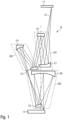
- Each module M1, M2, M3 can be individually removed from and reinserted into the projection lens 10. With appropriate adjustment devices, not only can the individual mirrors E1, E2, E3, E4, E5, E6 be adjusted, but also the individual modules M1, M2, M3, each as a whole, can be adjusted. This allows, on the one hand, the optical properties of the projection lens 10 to be quickly adapted to changing requirements by replacing one or more modules M1, M2, M3. On the other hand, reworking one of the optical elements of the projection lens 10 to correct imaging errors simply requires removing and, if necessary, disassembling the corresponding module M1, M2, or M3.
- modules M1, M2, and M3 are merely examples of possible modules.
- modules may contain more than two optical elements, such as three or four optical elements, or even just one optical element.
- the projection lens 10 may also contain fewer or more than three modules and, in particular, may also contain optical elements not included in any module.
- a modular design of other components of a projection exposure system for microlithography is also possible, such as a modular illumination system for illuminating the mask.
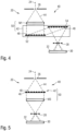
- Fig. 6 shows schematically an embodiment of a measuring arrangement 40 with a module M2 to be measured in the beam path 44, such as the optical module M2 of the projection lens 10 according to Fig. 1 , arranged first adaptation module 56 and a second adaptation module 58 arranged in the beam path 44 after the module M2.
- the adaptation modules 56, 58 each have a CGH 46, 60 operated in transmission with a diffractive structure pattern 48.
- the diffractive structures 48 of the two CGHs 46, 60 and thus also the two adaptation modules 56, 58 are configured such that, together with the module M2, they represent an imaging arrangement 50 for the opening of the pinhole 26.
- a double CGH enables simultaneous change of the location and direction of a measurement beam.
- an imaging property of the optical arrangement 50 can be better achieved with the adaptation module and the module M2 to be measured.
- the adaptation module 58 with the CGHs 60, 62 can achieve an optical effect that is more precisely adapted to the optical module M3 to be replaced.
- a double CGH is provided in the adaptation module 56 arranged in the beam path 44 upstream of the module M2, or in both adaptation modules 56, 58.
- two CGHs operated in reflection mode can also be used as a double CGH.
- further refractive, reflective, or diffractive optical elements can be arranged in one or both of the adaptation modules 56, 58.
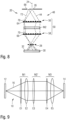
- FIG. 8 Furthermore, an embodiment of a measuring arrangement 40 according to Fig. 6 with a complex-coded CGH 64 or 66 in the adaptation modules 56 and 58 and a second pinhole 68.
- Each of the complex-coded CGHs 64, 66 contains two diffractive structure patterns 70 arranged superimposed on one another in the beam path 44.
- the diffractive structure patterns 70 are arranged superimposed on one another in a plane of the CGHs 64, 66.
- Such complex-coded CGHs are used, for example, in the DE 10 2012 217 800 A1 described.
- the measuring radiation 44 from the opening of the pinhole 26 is transformed by one of the diffractive structures of the CGHs 64, 66, while a measuring radiation 72 from the opening of the second pinhole 68 is transformed by the other diffractive structure of the CGHs 64 and 66.
- the adaptation modules 56 and 58 together with the module M2 represent an optical arrangement 50, which simultaneously controls the opening of the first pinhole 26 and the opening of the second pinhole 68 are imaged onto the shear grating 28. This allows two field points of the object plane of the optical arrangement 50 to be measured simultaneously.
- an adaptation module 42 with a complex coded CGH in front of a module M3 to be measured or analogous to the measuring device according to Fig. 3
- An adaptation module with a complex-coded CGH may be provided downstream of a module M1 to be measured.
- further refractive, reflective, or diffractive optical elements may be arranged in one or both of the adaptation modules 56, 58 or in an adaptation module 42 upstream or downstream of the optical module to be measured.
- Fig. 9 illustrates a further embodiment of a projection lens 10 of a projection exposure apparatus for microlithography.
- the projection lens 10 is designed for operation with UV radiation instead of EUV radiation, and thus the optical elements E1 to E5 are designed as lens elements.
- the projection lens 10 according to Fig. 9 comprises analogous to the embodiment according to Fig. 1 three optical modules M1, M2' and M3, wherein module M1 contains the optical elements E1 and E2, module M2' in the present case only the optical element E3 and module M3 the optical elements E4 and E5.
- module M2' can also contain multiple optical elements.
- Each of the modules M1, M2' and M3 represents an optical unit of the projection lens 10.
- Modules M1 and M3 are each formed by a partial arrangement of the optical elements E1 to E5 of the projection lens 10 and module M2' by only the optical element E3.
- the module M2' in the form of the optical element E3 is removed from the projection lens 10 according to Fig. 9 removed, so that the remaining modules M1 and M3 represent an optical unit formed by a partial arrangement of the optical elements E1 to E5, in which a gap 78 is present instead of the optical element E3.
- an adaptation module 74 corresponding to the optical function of the module M2' in the form of the optical element E3 is arranged.
- the adaptation module 74 contains a CGH operated in transmission with a diffractive structure pattern 76.
- the optical arrangement 50 formed by the module M1, the adaptation module 74 and the module M3 is measured by means of the wavefront measuring device 20 according to Fig. 2 This measurement allows the wavefront error of the sub-array formed by the combination of modules M1 and M3, consisting of the optical elements E1, E2, E4, and E5, to be determined very precisely.
- one of the described methods comprises determining wavefront errors of an entire imaging optical system on the basis of the wavefront errors determined for each sub-arrangement, in particular the wavefront errors determined for each module of the optical system.
- an embodiment of a measuring arrangement comprises a correspondingly designed evaluation device for determining wavefront errors of the imaging optical system based on the measurement results for each individual sub-arrangement of the optical system.
- Fig. 11 illustrates the calibration of an arrangement of two adjustment modules.
- the two adjustment modules are an input-side adjustment module 56 and an output-side adjustment module 58 for measuring the measuring module M2' of the projection lens 10 according to Fig. 9 .
- the measuring module M2' comprises only the optical element E3.
- the measuring arrangement is analogous to the measuring arrangement according to Fig. 6 built.
- the input-side matching module 56 is configured as a CGH with the optical function of module M1
- the output-side matching module 58 is configured as a CGH with the optical function of module M3.
- the arrangement of the two matching modules 56 and 58 is first calibrated.
- a calibration unit 80 which has the optical function of the optical unit to be measured in the form of the optical module M2', is arranged in place of the optical module M2' in the beam path 44 between the adaptation modules 56 and 58.
- the calibration unit 80 is configured as a CGH with a diffractive structure pattern 82.
- the calibration arrangement 82 consisting of the input-side adaptation module 56, the calibration unit 80, and the output-side adaptation module 58 is then measured using the wavefront measuring device 20. From the wavefront error determined in this process, the wavefront errors of the arrangement of the two adaptation modules 56 and 58 are determined as the calibration result, taking into account previously known wavefront errors of the calibration unit 80.
- the calibration module 80 is now replaced by the module M2', and the wavefront error determined in this process is corrected using the calibration result.
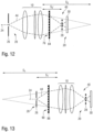
- the Figures 12 and 13 illustrate further embodiments of a measuring arrangement 40.
- the measuring arrangement 40 is used to measure an optical unit in the form of an imaging optical system, such as a projection lens 10 of a projection exposure apparatus for microlithography.
- the projection lens 10 shown is characterized by a very long output-side back focus s 2 or focal length in the
- the measurement arrangement 40 is characterized by a length of several meters, such as six meters.
- the arrangement comprises, in addition to the wavefront measuring device 20, an adaptation module 84 in the form of a CGH with a diffractive structure pattern 86 arranged downstream of the projection lens 10.
- the adaptation module 84 significantly shortens the output-side back focal length s 2 to a reduced back focal length s 2 ', in particular by at least a factor of 2, 3, or 4.
- the measuring arrangement 40 is according to Fig. 13 Configured to measure a projection lens 10, which is characterized by a very long input-side back focal length s 1 or focal length on the order of several meters.
- a projection lens 10 which is characterized by a very long input-side back focal length s 1 or focal length on the order of several meters.
- an adaptation module 88 in the form of a CGH with a diffractive structure pattern 90 positioned upstream of the projection lens 10.
- the adaptation module 88 significantly shortens the input-side back focal length s 1 to a reduced back focal length s 1 ', in particular by at least a factor of 2, 3, or 4.
- the adapters are adapted to the respective beam cross-section of the measuring radiation 44 present at the location of the adapter module.
- the surfaces described by the diffractive structural patterns can have, for example, a circular, elliptical, or crescent-shaped shape.
- the surfaces described by the diffractive structural patterns can have, for example, a circular, elliptical, or crescent-shaped shape.
- the areas of the diffractive structural patterns assigned to the individual field points overlap.
- FIG. 14 to 17 relate to embodiments of a measuring device and a method for interferometric shape measurement of optical surfaces according to a second aspect of the invention.
- the embodiments of a measuring device are each described together with embodiments of a corresponding method.
- Fig. 14 represents a first embodiment of a measuring device 100 for the interferometric shape measurement of optical surfaces.
- the measuring device 100 is suitable for the simultaneous measurement of at least two optical surfaces 102 and 104 arranged next to one another on a common substrate 106.
- the relative spatial position of the surfaces 102 and 104 to one another can also be determined.
- the optical surfaces 102 and 104 arranged on the same substrate 106 can, for example, assume the function of two mirror elements of a projection lens of a projection exposure system for EUV microlithography.
- the measuring device 100 contains an interferometer 108 with a Fizeau element 110.
- the interferometer 108 comprises a radiation source for generating electromagnetic illumination radiation 112 that is sufficiently coherent for an interferometric measurement.
- a laser e.g., a helium-neon laser with a wavelength of approximately 633 nm, can be provided.
- the illumination radiation 112 can also have a different wavelength in the visible or non-visible wavelength range of electromagnetic radiation.
- the illumination radiation 112 is formed, for example, by a collimator into a collimated beam with a substantially planar wavefront. In alternative embodiments, a divergent or convergent beam with a spherical wavefront can also be generated.
- the collimated beam impinges on the Fizeau element 110. A portion of the illumination radiation is reflected by a Fizeau surface of the Fizeau element 110 in the form of a reference wave 114. reflected back. A portion of the illumination radiation 112 passing through the Fizeau element 110 propagates as test radiation 116 further along the optical axis 118 of the interferometer 108 and impinges on a waveform element 120.
- a measuring radiation 117 is generated from the incident test radiation 116, which is composed of two measuring waves 128 and 130. After interacting with the optical surfaces 102 and 104 arranged in the beam path of the measuring waves 128 and 130 and other optical elements provided in the beam path, the measuring radiation 117 travels back through the Fizeau element 110 into the interferometer 108, where it is superimposed with the reference wave 114.
- An interferogram thus generated at a detection plane is recorded, for example, by a CCD sensor of an interferometer camera.
- a Michelson, a Twyman-Green interferometer or another suitable type of interferometer can also be used as the interferometer.
- the waveform element 120 contains a first diffractive structure 122 and a second diffractive structure 124, and in this exemplary embodiment is embodied as a CGH 126.
- the first and second diffractive structures 122, 124 are arranged side by side in a plane within the CGH 126.
- more than two diffractive structures can be arranged side by side in a plane of a CGH, or a complex-encoded CGH with two or more diffractive structures arranged superimposed on one plane can be provided as the waveform element.
- the first diffractive structure 122 is configured to generate a first measurement wave 128 directed toward the first optical surface 102 from a portion of the incident test radiation 116, with a wavefront adapted to a desired shape of the first surface 102.
- the second diffractive structure 124 is configured to generate a second measurement wave 130 directed toward the second optical surface 104 in the form of a measurement wave with a wavefront adapted to a desired shape of the second surface 104 from another portion of the test radiation 116 incident on the waveform element 120.
- the wavefronts are adapted such that the wavefronts of the measuring waves 128 and 130 correspond to the respective desired shape of the surfaces 102 and 104 at the location of the optical surfaces 102 and 104.
- a null optic is realized for the first and second optical surfaces 102 and 104, respectively, in which a surface in the desired shape would reflect the measuring wave 128 and 130 back into itself.
- additional diffractive structures on the CGH 126 or a complexly encoded CGH can be provided in further embodiments of the measuring device, each of which is configured to adapt the measuring radiation 117 accordingly for another optical surface.
- the substrate 106 with the optical surfaces 102 and 104 to be measured is arranged in the beam path of the test radiation 116 by means of a holding device (not shown).
- the respective measuring wave 128 or 130 is reflected back from the optical surfaces 102 and 104, in turn passes through the one-piece waveform element 120, and is then measured in the interferometer 108 by superimposing it with the reference wave 114.
- an interferogram is created in a detection plane for each of the surfaces 102 and 104 in the event of a deviation from the respective desired shape, which is detected, for example, by a CCD sensor of an interferometer camera (not shown).
- the measuring device 100 In addition to a simultaneous shape measurement of the two optical surfaces 102 and 104, the measuring device 100 also measures the relative positioning of the optical surfaces 102 and 104 to one another. This is described below with reference to Fig. 15 described in more detail. Finally, an evaluation device 158 determines the respective shape of the surfaces 102 and 104 as well as their relative position to one another. For this purpose, the evaluation device 158 uses the acquired interferograms and a measured relative position value of the optical surfaces 102 and 104 to one another for at least one rigid body degree of freedom. Alternatively, the acquired interferograms and the position value can also be stored for a later evaluation or transmission to an external evaluation facility.
- Fig. 15 shows the embodiment according to Fig. 14 with auxiliary waves 132 and 136 for determining a relative position of the optical surfaces 102 and 104 to one another.
- a first auxiliary measuring structure 134 is arranged in the CGH 126 of the waveform element 120 next to the diffractive structures 122 and 124.
- the first auxiliary measuring structure 134 contains a diffractive structure pattern configured to generate the first auxiliary wave 132, focused onto a target point 140 of the first surface 102, from a portion of the incident test radiation 116.
- a second auxiliary measurement structure 138 is arranged in addition to the diffractive structures 122 and 124 and the first auxiliary measurement structure 134.
- the second auxiliary measurement structure 138 contains a diffractive structure pattern, which is designed such that it generates a second auxiliary wave 136 focused on a target point 142 of the second surface 104 from a portion of the incident test radiation 116.
- auxiliary waves 132 and 136 After a back reflection of the auxiliary waves 132 and 136 at the respective points 140 and 142 of the optical surfaces 102 and 104, they are interferometrically measured in the interferometer 108 by superimposing them with the reference wave 114. With the aid of the evaluation unit, a deviation of the optical surface 102 or 104 at the respective point 140 or 142 from the desired focal point is measured very precisely. Together with the angles determined by the auxiliary measuring structures 134 and 138 between the optical axis 118 of the interferometer 108 and the propagation directions of the auxiliary waves 132 and 136, for example, the relative z-coordinate of the optical surfaces 102 and 104 to each other with respect to the points 140, 142 is determined.
- the z-axis of the coordinate system describing the relative position of the surfaces 102, 104 to each other is here parallel to the optical axis 118 or essentially parallel to the mean propagation direction of the measuring radiation 117 and thus transverse to the optical surfaces 102 and 104.
- the relative x-coordinate, y-coordinate, and tilt coordinates of the two optical surfaces 102 and 104 to each other are then determined by evaluating the measured reflected measuring waves of the surface measurement or the determined shapes of the surfaces 102 and 104, taking into account the known relative z-coordinate.
- additional auxiliary measurement structures for auxiliary waves can be provided on the waveform element in order to determine a deviation of additional points on the optical surfaces from a desired focus.
- additional planar or spherical adjustment structures can be arranged next to the optical surfaces on the substrate, whose spatial position is measured using auxiliary waves with a planar or spherical wavefront.
- Fig. 16 shows a further embodiment of a measuring device 100 for the simultaneous shape measurement of adjacent optical surfaces 102 and 104.
- the measuring device 100 essentially corresponds to the measuring device according to Fig. 14 and Fig. 15 .
- the first diffractive structure 122 of the CGH 126 of the waveform element 120 is configured such that it generates from a portion of the measuring radiation 116 a measuring wave 128 directed only onto a first partial region 144 of the first optical surface 102 with a wavefront adapted to a desired shape of the first partial region 144.
- a further waveform element 148 with a correspondingly configured diffractive structure 150 is provided in a CGH 152.
- the waveform elements 120 and 148 are exchanged in the measuring device 100.
- the measuring device 100 can have an exchange device (not shown).
- a measurement of the second partial region 146 is performed using the second waveform element 148.
- the partial measurement is combined into an overall measurement of the optical surface 102 by the evaluation device 158 using a so-called stitching method or another suitable method.
Landscapes
- Physics & Mathematics (AREA)
- General Physics & Mathematics (AREA)
- Health & Medical Sciences (AREA)
- Engineering & Computer Science (AREA)
- Environmental & Geological Engineering (AREA)
- Epidemiology (AREA)
- Public Health (AREA)
- Geometry (AREA)
- Chemical & Material Sciences (AREA)
- Analytical Chemistry (AREA)
- Exposure And Positioning Against Photoresist Photosensitive Materials (AREA)
- Testing Of Optical Devices Or Fibers (AREA)
- Diffracting Gratings Or Hologram Optical Elements (AREA)
Claims (15)
- Dispositif de mesure (40) pour mesurer une unité optique (M1 ; M2 ; M3 ; M1, M3, 10) d'un système d'exposition par projection pour la microlithographie, comprenant :- un dispositif (20) de mesure de front d'onde qui est configuré pour mesurer, au moyen d'une interférométrie à décalage de phase, une aberration de front d'onde d'une optique (22) de formation d'image au moyen d'un rayonnement de mesure (72), et qui comprend un diaphragme à trou ou un masque de cohérence ainsi qu'un réseau de diffraction, et- au moins un module d'adaptation (42 ; 56, 58 ; 84) qui est configuré pour manipuler le front d'onde du rayonnement de mesure de telle sorte que la combinaison de l'unité optique à mesurer et dudit au moins un module d'adaptation forme un ensemble optique de formation d'images (50) qui forme une image d'une ouverture du diaphragme à trou ou du masque de cohérence sur le réseau de diffraction,le dispositif de mesure étant en outre configuré pour déterminer une aberration de front d'onde de l'unité optique à mesurer, à partir d'une aberration de front d'onde mesurée au moyen du dispositif de mesure de front d'onde de l'ensemble optique de formation d'image formé par la combinaison, en soustrayant une aberration de front d'onde connue au préalable du module d'adaptation (42 ; 56 ; 58 ; 84).
- Dispositif de mesure selon la revendication 1,
dans lequel l'unité optique est associée à un système optique (10) de formation d'image comprenant plusieurs éléments optiques d'un dispositif d'exposition par projection pour la microlithographie, et l'unité optique étant déviée par l'un des éléments optiques du système optique de formation d'image, par un sous-ensemble (M1 ; M2 ; M3 ; M1, M3) des éléments optiques du système optique (10) de formation d'image ou par le système optique (10) de formation d'image. - Dispositif de mesure selon la revendication 2,
dans lequel l'unité optique est formée par un sous-ensemble des éléments optiques du système optique de formation d'image, le sous-ensemble des éléments optiques se distinguant d'au moins une partie du système optique de formation d'image par la présence d'un espace (78) concernant au moins un élément optique. - Dispositif de mesure selon l'une des revendications précédentes,
dans lequel le module d'adaptation est configuré de manière à raccourcir une distance focale de l'unité optique (10) à mesurer. - Dispositif de mesure selon l'une des revendications précédentes,
qui comprend en outre une unité d'étalonnage (80) comprenant la fonction optique de l'unité optique à mesurer, qui est configurée de manière à étalonner, avant la mesure de l'unité optique, ledit au moins un module d'adaptation (56, 58) en déterminant une aberration de front d'onde d'un agencement comprenant ledit au moins un module d'adaptation ainsi que l'unité d'étalonnage. - Dispositif de mesure selon l'une des revendications précédentes,
dans lequel ledit au moins un module d'adaptation comprend une ou plusieurs structures diffractives fonctionnant en réflexion ou en transmission. - Dispositif de mesure selon l'une des revendications précédentes,
dans lequel ledit au moins un module d'adaptation comprend au moins deux motifs de structure diffractive (70) superposés ou agencés l'un derrière l'autre dans un trajet de faisceau du rayonnement de mesure. - Procédé de mesure d'une unité optique (M1 ; M2 ; M3 ; M1, M3, 10) d'un objectif de projection (10) d'un dispositif d'exposition par projection pour la microlithographie, comprenant les étapes suivantes :- agencer au moins un module d'adaptation (42 ; 56, 58 ; 84) sur l'unité optique à mesurer de telle sorte que la combinaison de l'unité optique à mesurer et dudit au moins un module d'adaptation forme un dispositif optique de formation d'image (50) qui forme une image d'une ouverture d'un diaphragme à trou ou d'un masque de cohérence sur un réseau de diffraction,- mesurer, au moyen d'une interférométrie à décalage de phase, une aberration de front d'onde du dispositif optique de formation d'image formé par la combinaison, et- déterminer une aberration de front d'onde de l'unité optique à mesurer à partir de l'aberration de front d'onde mesurée de l'ensemble optique formé par la combinaison, en soustrayant une aberration de front d'onde connue au préalable du module d'adaptation (42 ; 56 ; 58 ; 84).
- Procédé selon la revendication 8,
dans lequel l'unité optique à mesurer est configurée sous la forme d'une optique non imageante qui, lors de l'incidence d'une onde d'entrée plane ou sphérique d'une longueur d'onde λ, génère une onde de sortie dont le front d'onde s'écarte d'au moins λ d'une onde sphérique idéale en au moins un point. - Procédé de mesure d'une aberration de front d'onde d'un système optique (10) de formation d'image d'une installation d'exposition par projection pour la microlithographie, comportant plusieurs éléments optiques (E1-E6) pour former l'image d'un motif à partir d'un plan objet dans un plan image,
les aberrations de front d'onde respectives de différents sous-ensembles (M1 ; M2 ; M3 ; M1, M3) des éléments optiques étant mesurées séparément. - Procédé selon la revendication 10,
dans lequel l'un des sous-ensembles des éléments optiques se distinguant d'au moins une partie du système optique de formation d'image par la présence d'un espace (78) concernant au moins un élément optique. - Procédé selon la revendication 10 ou la revendication 11,
dans lequel le système optique de formation d'image est pourvu d'une pluralité de modules optiques comprenant chacun au moins deux des éléments optiques, et la mesure séparée des erreurs de front d'onde respectives de différents sous-ensembles étant effectuée par une mesure séparée des erreurs de front d'onde respectives des différents modules optiques (M1 ; M2 ; M3). - Procédé selon l'une des revendications 10 à 12,
dans lequel la mesure d'un des sous-ensembles nécessite un agencement du sous-ensemble à mesurer et d'au moins un module d'adaptation dans le trajet du faisceau d' un rayonnement de mesure (72) d'un dispositif (20) de mesure de front d'onde, tel que la combinaison du sous-ensemble à mesurer et dudit au moins un module d'adaptation forme un ensemble optique de formation d'image (50), et la mesure comprend en outre une détermination de l'aberration de front d'onde de l'ensemble optique de formation d'image au moyen du dispositif de mesure de front d'onde. - Procédé selon la revendication 13,
dans lequel l'agencement dudit au moins un module d'adaptation comprend un agencement d'un module d'adaptation côté entrée (56) pour manipuler le rayonnement de mesure avant le sous-ensemble à mesurer, et un agencement d'un module d'adaptation côté sortie (58) pour manipuler le rayonnement de mesure après le sous-ensemble à mesurer. - Procédé selon la revendication 13 ou la revendication 14,
dans lequel au moins un motif structurel diffractif (48) est utilisé dans ledit au moins un module d'adaptation pour manipuler le front d'onde du rayonnement de mesure.
Applications Claiming Priority (4)
| Application Number | Priority Date | Filing Date | Title |
|---|---|---|---|
| DE102015209173.2A DE102015209173B4 (de) | 2015-05-20 | 2015-05-20 | Verfahren zum herstellen eines objektivs für eine lithographieanlage |
| DE102015220588.6A DE102015220588A1 (de) | 2015-10-22 | 2015-10-22 | Messverfahren und Messanordnung für ein abbildendes optisches System |
| DE102016203562.2A DE102016203562A1 (de) | 2016-03-04 | 2016-03-04 | Messverfahren und Messanordnung für ein abbildendes optisches System |
| PCT/EP2016/000832 WO2016184571A2 (fr) | 2015-05-20 | 2016-05-19 | Procédé de mesure et ensemble de mesure pour un système optique de formation d'image |
Publications (3)
| Publication Number | Publication Date |
|---|---|
| EP3298446A2 EP3298446A2 (fr) | 2018-03-28 |
| EP3298446C0 EP3298446C0 (fr) | 2025-07-02 |
| EP3298446B1 true EP3298446B1 (fr) | 2025-07-02 |
Family
ID=56108599
Family Applications (1)
| Application Number | Title | Priority Date | Filing Date |
|---|---|---|---|
| EP16727302.8A Active EP3298446B1 (fr) | 2015-05-20 | 2016-05-19 | Procédé de mesure et ensemble de mesure pour un système optique de formation d'image |
Country Status (5)
| Country | Link |
|---|---|
| US (1) | US10502545B2 (fr) |
| EP (1) | EP3298446B1 (fr) |
| JP (1) | JP6783801B2 (fr) |
| KR (1) | KR102598505B1 (fr) |
| WO (1) | WO2016184571A2 (fr) |
Families Citing this family (13)
| Publication number | Priority date | Publication date | Assignee | Title |
|---|---|---|---|---|
| DE102017217251A1 (de) | 2017-09-27 | 2019-03-28 | Carl Zeiss Smt Gmbh | Verfahren und Anordnung zur Analyse der Wellenfrontwirkung eines optischen Systems |
| DE102017221005A1 (de) * | 2017-11-23 | 2019-05-23 | Carl Zeiss Smt Gmbh | Verfahren und Vorrichtung zur Kalibrierung einer diffraktiven Messstruktur |
| DE102018216344A1 (de) * | 2018-09-25 | 2020-03-26 | Carl Zeiss Smt Gmbh | Abstützung eines optischen elements |
| CN109739027B (zh) * | 2019-01-16 | 2021-07-27 | 北京华捷艾米科技有限公司 | 光点阵投影模组和深度相机 |
| DE102019201762A1 (de) * | 2019-02-12 | 2020-08-13 | Carl Zeiss Smt Gmbh | Vorrichtung und Verfahren zur Charakterisierung der Oberflächenform eines Testobjekts |
| DE102019204096A1 (de) * | 2019-03-26 | 2020-10-01 | Carl Zeiss Smt Gmbh | Messverfahren zur interferometrischen Bestimmung einer Oberflächenform |
| WO2020227000A1 (fr) * | 2019-05-03 | 2020-11-12 | California Institute Of Technology | Imageur de métasurface pour détection quantitative de gradient de phase |
| CN112147851B (zh) * | 2019-06-28 | 2022-03-11 | 上海微电子装备(集团)股份有限公司 | 光刻设备及光刻设备的瞳面透过率的检测方法 |
| CN110441992B (zh) * | 2019-07-23 | 2020-05-05 | 中国科学院上海光学精密机械研究所 | 投影物镜波像差检测装置及检测方法 |
| CN111103769B (zh) * | 2020-01-02 | 2021-09-07 | 中国科学院上海光学精密机械研究所 | 对光强波动不敏感的投影物镜波像差检测装置与检测方法 |
| US12053240B2 (en) | 2020-05-20 | 2024-08-06 | Arizona Optical Metrology Llc | Systems and methods for measurement of optical wavefronts |
| US11609506B2 (en) * | 2021-04-21 | 2023-03-21 | Kla Corporation | System and method for lateral shearing interferometry in an inspection tool |
| DE102022107686A1 (de) * | 2022-03-31 | 2023-10-05 | Trioptics Gmbh | Verfahren und Vorrichtung zum Bestimmen einer Abbildungsqualität eines zu prüfenden optischen Systems |
Citations (3)
| Publication number | Priority date | Publication date | Assignee | Title |
|---|---|---|---|---|
| DE10316123A1 (de) * | 2003-04-04 | 2004-10-14 | Carl Zeiss Smt Ag | Vorrichtung und Verfahren zur Wellenfrontvermessung eines optischen Abbildungssystems durch phasenschiebende Interferometrie |
| US20060093793A1 (en) * | 2003-06-19 | 2006-05-04 | Nikon Corporation | Optical element |
| US20060146342A1 (en) * | 2005-01-04 | 2006-07-06 | Carl Zeiss Smt Ag | Phase shifting interferometric method, interferometer apparatus and method of manufacturing an optical element |
Family Cites Families (35)
| Publication number | Priority date | Publication date | Assignee | Title |
|---|---|---|---|---|
| AT402860B (de) * | 1993-06-22 | 1997-09-25 | Oesterr Forsch Seibersdorf | Verfahren und vorrichtung zur prüfung von transparenten gegenständen |
| US6271914B1 (en) * | 1996-11-25 | 2001-08-07 | Autonomous Technologies Corporation | Objective measurement and correction of optical systems using wavefront analysis |
| DE19818341B4 (de) * | 1998-04-23 | 2008-06-26 | Schneider Gmbh & Co. Kg | Interferometer zum Vermessen asphärischer Linsen |
| TW550377B (en) | 2000-02-23 | 2003-09-01 | Zeiss Stiftung | Apparatus for wave-front detection |
| JP2002184667A (ja) * | 2000-12-14 | 2002-06-28 | Nikon Corp | 補正部材の製造方法、投影光学系の製造方法および露光装置の調整方法 |
| JPWO2002052620A1 (ja) * | 2000-12-22 | 2004-04-30 | 株式会社ニコン | 波面収差測定装置、波面収差測定方法、露光装置及びマイクロデバイスの製造方法 |
| JP2002289515A (ja) | 2000-12-28 | 2002-10-04 | Nikon Corp | 製品の製造方法、露光装置の製造方法、露光装置、及びデバイス製造方法 |
| DE10113017A1 (de) | 2001-03-17 | 2002-09-26 | Zeiss Carl | System zur interferometrischen Messung von optisch wirksamen Fehlern von optischen Baugruppen |
| JP2003332200A (ja) * | 2002-05-09 | 2003-11-21 | Nikon Corp | 光学系の測定方法、光学系の補正方法、光学系の評価方法、投影光学系の製造方法、及び投影光学系 |
| JP2004128307A (ja) | 2002-10-04 | 2004-04-22 | Nikon Corp | 露光装置及びその調整方法 |
| JP4266673B2 (ja) * | 2003-03-05 | 2009-05-20 | キヤノン株式会社 | 収差測定装置 |
| AU2004291042B2 (en) * | 2003-11-14 | 2010-10-14 | Essilor International (Compagnie Generale D'optique) | Ophthalmic binocular wafefront measurement system |
| US20050105044A1 (en) * | 2003-11-14 | 2005-05-19 | Laurence Warden | Lensometers and wavefront sensors and methods of measuring aberration |
| US7336371B1 (en) * | 2004-01-29 | 2008-02-26 | Carl Zeiss Smt Ag | Apparatus and method for measuring the wavefront of an optical system |
| US7728987B2 (en) | 2004-05-14 | 2010-06-01 | Carl Zeiss Smt Ag | Method of manufacturing an optical element |
| DE102006014510A1 (de) * | 2005-04-15 | 2006-10-19 | Carl Zeiss Smt Ag | Optische Detektionsvorrichtung, Messvorrichtung und Verwendung |
| EP1987390A1 (fr) | 2005-05-24 | 2008-11-05 | Carl Zeiss SMT AG | Procede d'alignement d'un systeme optique |
| US7688701B2 (en) * | 2005-06-20 | 2010-03-30 | Konica Minolta Opto, Inc. | Objective optical system and optical pickup apparatus |
| US7605926B1 (en) | 2005-09-21 | 2009-10-20 | Carl Zeiss Smt Ag | Optical system, method of manufacturing an optical system and method of manufacturing an optical element |
| DE102006035022A1 (de) * | 2006-07-28 | 2008-01-31 | Carl Zeiss Smt Ag | Verfahren zum Herstellen einer optischen Komponente, Interferometeranordnung und Beugungsgitter |
| WO2008110239A1 (fr) | 2007-03-15 | 2008-09-18 | Carl Zeiss Smt Ag | Composant diffractif, agencement d'interféromètre, procédé de qualification de réseau de diffraction double, procédé de fabrication d'un élément optique, et procédé d'interférométrie |
| US20090147228A1 (en) | 2007-12-11 | 2009-06-11 | Nikon Corporation | Exposure apparatus, manufacturing method thereof, and maintenance method of exposure apparatus |
| JP5450975B2 (ja) * | 2008-04-10 | 2014-03-26 | キヤノン株式会社 | 測定装置および測定方法 |
| US20110001945A1 (en) | 2009-07-01 | 2011-01-06 | Masayuki Shiraishi | Projection optical system, exposure apparatus, and assembly method thereof |
| DE102010038748A1 (de) | 2009-08-07 | 2011-03-24 | Carl Zeiss Smt Gmbh | Verfahren zur Herstellung eines Spiegels mit wenigstens zwei Spiegelflächen, Spiegel einer Projektionsbelichtungsanlage der Mikrolithographie und Projektionsbelichtungsanlage |
| US9389519B2 (en) * | 2010-02-25 | 2016-07-12 | Nikon Corporation | Measuring method and measuring apparatus of pupil transmittance distribution, exposure method and exposure apparatus, and device manufacturing method |
| DE102010038697B4 (de) | 2010-07-30 | 2012-07-19 | Carl Zeiss Smt Gmbh | Verfahren und Vorrichtung zur Qualifizierung einer Optik einer Projektionsbelichtungsanlage für die Mikrolithographie |
| DE102011006468B4 (de) * | 2011-03-31 | 2014-08-28 | Carl Zeiss Smt Gmbh | Vermessung eines abbildenden optischen Systems durch Überlagerung von Mustern |
| DE102012202057B4 (de) | 2012-02-10 | 2021-07-08 | Carl Zeiss Smt Gmbh | Projektionsobjektiv für EUV-Mikrolithographie, Folienelement und Verfahren zur Herstellung eines Projektionsobjektivs mit Folienelement |
| DE102012211256A1 (de) * | 2012-06-29 | 2014-01-02 | Carl Zeiss Smt Gmbh | Projektionsbelichtungsanlage für die Projektionslithographie |
| DE102012217800A1 (de) | 2012-09-28 | 2014-04-03 | Carl Zeiss Smt Gmbh | Diffraktives optisches Element sowie Messverfahren |
| DE102014226269A1 (de) * | 2014-12-17 | 2016-06-23 | Carl Zeiss Smt Gmbh | Wellenfrontmesseinrichtung, Projektionsobjektiv mit einer solchen Messeinrichtung und mit einer solchen Messeinrichtung zusammenwirkender optischer Wellenfrontmanipulator |
| DE102015202695A1 (de) | 2015-02-13 | 2016-08-18 | Carl Zeiss Smt Gmbh | Prüfvorrichtung sowie Verfahren zum Prüfen eines Spiegels |
| DE102015220588A1 (de) | 2015-10-22 | 2017-04-27 | Carl Zeiss Smt Gmbh | Messverfahren und Messanordnung für ein abbildendes optisches System |
| DE102015226571B4 (de) | 2015-12-22 | 2019-10-24 | Carl Zeiss Smt Gmbh | Vorrichtung und Verfahren zur Wellenfrontanalyse |
-
2016
- 2016-05-19 WO PCT/EP2016/000832 patent/WO2016184571A2/fr not_active Ceased
- 2016-05-19 JP JP2017560198A patent/JP6783801B2/ja active Active
- 2016-05-19 EP EP16727302.8A patent/EP3298446B1/fr active Active
- 2016-05-19 KR KR1020177036207A patent/KR102598505B1/ko active Active
-
2017
- 2017-11-20 US US15/818,080 patent/US10502545B2/en active Active
Patent Citations (3)
| Publication number | Priority date | Publication date | Assignee | Title |
|---|---|---|---|---|
| DE10316123A1 (de) * | 2003-04-04 | 2004-10-14 | Carl Zeiss Smt Ag | Vorrichtung und Verfahren zur Wellenfrontvermessung eines optischen Abbildungssystems durch phasenschiebende Interferometrie |
| US20060093793A1 (en) * | 2003-06-19 | 2006-05-04 | Nikon Corporation | Optical element |
| US20060146342A1 (en) * | 2005-01-04 | 2006-07-06 | Carl Zeiss Smt Ag | Phase shifting interferometric method, interferometer apparatus and method of manufacturing an optical element |
Also Published As
| Publication number | Publication date |
|---|---|
| EP3298446C0 (fr) | 2025-07-02 |
| JP6783801B2 (ja) | 2020-11-11 |
| KR20180010213A (ko) | 2018-01-30 |
| WO2016184571A2 (fr) | 2016-11-24 |
| WO2016184571A3 (fr) | 2016-12-29 |
| KR102598505B1 (ko) | 2023-11-06 |
| US20180087891A1 (en) | 2018-03-29 |
| JP2018524625A (ja) | 2018-08-30 |
| EP3298446A2 (fr) | 2018-03-28 |
| US10502545B2 (en) | 2019-12-10 |
Similar Documents
| Publication | Publication Date | Title |
|---|---|---|
| EP3298446B1 (fr) | Procédé de mesure et ensemble de mesure pour un système optique de formation d'image | |
| EP3256835B1 (fr) | Dispositif de test et procédé de test d'un miroir | |
| EP3298343B1 (fr) | Dispositif de mesure interférométrique | |
| EP3948156B1 (fr) | Procédé de mesure pour la détermination interférométrique d'une forme de surface | |
| EP3224570B1 (fr) | Procédé et dispositif de test interférométrique | |
| WO2008012091A2 (fr) | Procédé et dispositif de détermination de l'écart d'une forme réelle de la forme nominale d'une surface optique | |
| DE102015202676B4 (de) | Interferometrische Messvorrichtung | |
| DE102018209175B4 (de) | Computer-generiertes Hologramm (CGH), interferometrische Prüfanordnung, sowie Verfahren zur Charakterisierung der Oberflächenform eines optischen Elements | |
| DE102013218991A1 (de) | Vorrichtung zum Bestimmen einer optischen Eigenschaft eines optischen Abbildungssystems | |
| WO2021032587A2 (fr) | Procédé d'étalonnage d'un dispositif de mesure | |
| DE102021202909A1 (de) | Messvorrichtung zum interferometrischen Vermessen einer Oberflächenform | |
| DE102010038748A1 (de) | Verfahren zur Herstellung eines Spiegels mit wenigstens zwei Spiegelflächen, Spiegel einer Projektionsbelichtungsanlage der Mikrolithographie und Projektionsbelichtungsanlage | |
| WO2015150301A1 (fr) | Procédé pour ajuster un miroir d'un appareil d'éclairement par projection microlithographique | |
| DE102015220588A1 (de) | Messverfahren und Messanordnung für ein abbildendes optisches System | |
| DE102023206874A1 (de) | Interferometrische Messvorrichtung | |
| DE102016212464A1 (de) | Messvorrichtung zum Bestimmen eines Wellenfrontfehlers | |
| DE102020207946A1 (de) | Messvorrichtung zur interferometrischen Bestimmung einer Oberflächenform | |
| DE102018203795A1 (de) | Interferometrische Messanordnung zur Bestimmung einer Oberflächenform | |
| WO2024056501A1 (fr) | Procédé de traitement d'un élément de référence pour un interféromètre | |
| WO2021063766A1 (fr) | Dspositif de mesure pour déterminer par interférométrie la forme d'une surface | |
| DE102015209489A1 (de) | Interferometrische Messvorrichtung | |
| EP4336139A1 (fr) | Procédé d'étalonnage d'un arbre sphérique et système d'inspection pour déterminer par interférométrie la forme de surface d'un échantillon | |
| DE102016203562A1 (de) | Messverfahren und Messanordnung für ein abbildendes optisches System | |
| WO2022037898A1 (fr) | Procédé et dispositif pour caractériser la forme de la surface d'un élément optique | |
| DE102021203123A1 (de) | Computer-generiertes Hologramm (CGH) sowie interferometrische Messanordnung zur Bestimmung der Oberflächenform eines Prüflings |
Legal Events
| Date | Code | Title | Description |
|---|---|---|---|
| STAA | Information on the status of an ep patent application or granted ep patent |
Free format text: STATUS: THE INTERNATIONAL PUBLICATION HAS BEEN MADE |
|
| PUAI | Public reference made under article 153(3) epc to a published international application that has entered the european phase |
Free format text: ORIGINAL CODE: 0009012 |
|
| STAA | Information on the status of an ep patent application or granted ep patent |
Free format text: STATUS: REQUEST FOR EXAMINATION WAS MADE |
|
| 17P | Request for examination filed |
Effective date: 20171220 |
|
| AK | Designated contracting states |
Kind code of ref document: A2 Designated state(s): AL AT BE BG CH CY CZ DE DK EE ES FI FR GB GR HR HU IE IS IT LI LT LU LV MC MK MT NL NO PL PT RO RS SE SI SK SM TR |
|
| AX | Request for extension of the european patent |
Extension state: BA ME |
|
| DAV | Request for validation of the european patent (deleted) | ||
| DAX | Request for extension of the european patent (deleted) | ||
| STAA | Information on the status of an ep patent application or granted ep patent |
Free format text: STATUS: EXAMINATION IS IN PROGRESS |
|
| 17Q | First examination report despatched |
Effective date: 20200207 |
|
| GRAP | Despatch of communication of intention to grant a patent |
Free format text: ORIGINAL CODE: EPIDOSNIGR1 |
|
| STAA | Information on the status of an ep patent application or granted ep patent |
Free format text: STATUS: GRANT OF PATENT IS INTENDED |
|
| RIC1 | Information provided on ipc code assigned before grant |
Ipc: G03F 7/00 20060101ALI20241008BHEP Ipc: G01M 11/02 20060101ALI20241008BHEP Ipc: G02B 7/00 20060101AFI20241008BHEP |
|
| INTG | Intention to grant announced |
Effective date: 20241030 |
|
| GRAJ | Information related to disapproval of communication of intention to grant by the applicant or resumption of examination proceedings by the epo deleted |
Free format text: ORIGINAL CODE: EPIDOSDIGR1 |
|
| STAA | Information on the status of an ep patent application or granted ep patent |
Free format text: STATUS: EXAMINATION IS IN PROGRESS |
|
| GRAP | Despatch of communication of intention to grant a patent |
Free format text: ORIGINAL CODE: EPIDOSNIGR1 |
|
| STAA | Information on the status of an ep patent application or granted ep patent |
Free format text: STATUS: GRANT OF PATENT IS INTENDED |
|
| INTC | Intention to grant announced (deleted) | ||
| INTG | Intention to grant announced |
Effective date: 20250113 |
|
| GRAS | Grant fee paid |
Free format text: ORIGINAL CODE: EPIDOSNIGR3 |
|
| GRAA | (expected) grant |
Free format text: ORIGINAL CODE: 0009210 |
|
| STAA | Information on the status of an ep patent application or granted ep patent |
Free format text: STATUS: THE PATENT HAS BEEN GRANTED |
|
| AK | Designated contracting states |
Kind code of ref document: B1 Designated state(s): AL AT BE BG CH CY CZ DE DK EE ES FI FR GB GR HR HU IE IS IT LI LT LU LV MC MK MT NL NO PL PT RO RS SE SI SK SM TR |
|
| REG | Reference to a national code |
Ref country code: GB Ref legal event code: FG4D Free format text: NOT ENGLISH |
|
| REG | Reference to a national code |
Ref country code: CH Ref legal event code: EP |
|
| REG | Reference to a national code |
Ref country code: DE Ref legal event code: R096 Ref document number: 502016017011 Country of ref document: DE |
|
| REG | Reference to a national code |
Ref country code: IE Ref legal event code: FG4D Free format text: LANGUAGE OF EP DOCUMENT: GERMAN |
|
| U01 | Request for unitary effect filed |
Effective date: 20250708 |
|
| U07 | Unitary effect registered |
Designated state(s): AT BE BG DE DK EE FI FR IT LT LU LV MT NL PT RO SE SI Effective date: 20250714 |
|
| PG25 | Lapsed in a contracting state [announced via postgrant information from national office to epo] |
Ref country code: IS Free format text: LAPSE BECAUSE OF FAILURE TO SUBMIT A TRANSLATION OF THE DESCRIPTION OR TO PAY THE FEE WITHIN THE PRESCRIBED TIME-LIMIT Effective date: 20251102 |
|
| PG25 | Lapsed in a contracting state [announced via postgrant information from national office to epo] |
Ref country code: NO Free format text: LAPSE BECAUSE OF FAILURE TO SUBMIT A TRANSLATION OF THE DESCRIPTION OR TO PAY THE FEE WITHIN THE PRESCRIBED TIME-LIMIT Effective date: 20251002 |
|
| PG25 | Lapsed in a contracting state [announced via postgrant information from national office to epo] |
Ref country code: HR Free format text: LAPSE BECAUSE OF FAILURE TO SUBMIT A TRANSLATION OF THE DESCRIPTION OR TO PAY THE FEE WITHIN THE PRESCRIBED TIME-LIMIT Effective date: 20250702 |
|
| PG25 | Lapsed in a contracting state [announced via postgrant information from national office to epo] |
Ref country code: GR Free format text: LAPSE BECAUSE OF FAILURE TO SUBMIT A TRANSLATION OF THE DESCRIPTION OR TO PAY THE FEE WITHIN THE PRESCRIBED TIME-LIMIT Effective date: 20251003 |
|
| PG25 | Lapsed in a contracting state [announced via postgrant information from national office to epo] |
Ref country code: CZ Free format text: LAPSE BECAUSE OF FAILURE TO SUBMIT A TRANSLATION OF THE DESCRIPTION OR TO PAY THE FEE WITHIN THE PRESCRIBED TIME-LIMIT Effective date: 20250702 |
|
| PG25 | Lapsed in a contracting state [announced via postgrant information from national office to epo] |
Ref country code: PL Free format text: LAPSE BECAUSE OF FAILURE TO SUBMIT A TRANSLATION OF THE DESCRIPTION OR TO PAY THE FEE WITHIN THE PRESCRIBED TIME-LIMIT Effective date: 20250702 |
|
| PG25 | Lapsed in a contracting state [announced via postgrant information from national office to epo] |
Ref country code: RS Free format text: LAPSE BECAUSE OF FAILURE TO SUBMIT A TRANSLATION OF THE DESCRIPTION OR TO PAY THE FEE WITHIN THE PRESCRIBED TIME-LIMIT Effective date: 20251002 |
|
| PG25 | Lapsed in a contracting state [announced via postgrant information from national office to epo] |
Ref country code: ES Free format text: LAPSE BECAUSE OF FAILURE TO SUBMIT A TRANSLATION OF THE DESCRIPTION OR TO PAY THE FEE WITHIN THE PRESCRIBED TIME-LIMIT Effective date: 20250702 |
|
| PG25 | Lapsed in a contracting state [announced via postgrant information from national office to epo] |
Ref country code: SM Free format text: LAPSE BECAUSE OF FAILURE TO SUBMIT A TRANSLATION OF THE DESCRIPTION OR TO PAY THE FEE WITHIN THE PRESCRIBED TIME-LIMIT Effective date: 20250702 |
|
| PG25 | Lapsed in a contracting state [announced via postgrant information from national office to epo] |
Ref country code: SK Free format text: LAPSE BECAUSE OF FAILURE TO SUBMIT A TRANSLATION OF THE DESCRIPTION OR TO PAY THE FEE WITHIN THE PRESCRIBED TIME-LIMIT Effective date: 20250702 |