EP3298480B1 - Anzeigemodul und verfahren zur herstellung davon - Google Patents
Anzeigemodul und verfahren zur herstellung davon Download PDFInfo
- Publication number
- EP3298480B1 EP3298480B1 EP15893458.8A EP15893458A EP3298480B1 EP 3298480 B1 EP3298480 B1 EP 3298480B1 EP 15893458 A EP15893458 A EP 15893458A EP 3298480 B1 EP3298480 B1 EP 3298480B1
- Authority
- EP
- European Patent Office
- Prior art keywords
- display module
- particles
- display
- panel
- conductive
- Prior art date
- Legal status (The legal status is an assumption and is not a legal conclusion. Google has not performed a legal analysis and makes no representation as to the accuracy of the status listed.)
- Active
Links
Images



Classifications
-
- G—PHYSICS
- G06—COMPUTING OR CALCULATING; COUNTING
- G06F—ELECTRIC DIGITAL DATA PROCESSING
- G06F3/00—Input arrangements for transferring data to be processed into a form capable of being handled by the computer; Output arrangements for transferring data from processing unit to output unit, e.g. interface arrangements
- G06F3/01—Input arrangements or combined input and output arrangements for interaction between user and computer
- G06F3/03—Arrangements for converting the position or the displacement of a member into a coded form
- G06F3/041—Digitisers, e.g. for touch screens or touch pads, characterised by the transducing means
-
- C—CHEMISTRY; METALLURGY
- C09—DYES; PAINTS; POLISHES; NATURAL RESINS; ADHESIVES; COMPOSITIONS NOT OTHERWISE PROVIDED FOR; APPLICATIONS OF MATERIALS NOT OTHERWISE PROVIDED FOR
- C09D—COATING COMPOSITIONS, e.g. PAINTS, VARNISHES OR LACQUERS; FILLING PASTES; CHEMICAL PAINT OR INK REMOVERS; INKS; CORRECTING FLUIDS; WOODSTAINS; PASTES OR SOLIDS FOR COLOURING OR PRINTING; USE OF MATERIALS THEREFOR
- C09D11/00—Inks
- C09D11/02—Printing inks
- C09D11/03—Printing inks characterised by features other than the chemical nature of the binder
-
- C—CHEMISTRY; METALLURGY
- C09—DYES; PAINTS; POLISHES; NATURAL RESINS; ADHESIVES; COMPOSITIONS NOT OTHERWISE PROVIDED FOR; APPLICATIONS OF MATERIALS NOT OTHERWISE PROVIDED FOR
- C09D—COATING COMPOSITIONS, e.g. PAINTS, VARNISHES OR LACQUERS; FILLING PASTES; CHEMICAL PAINT OR INK REMOVERS; INKS; CORRECTING FLUIDS; WOODSTAINS; PASTES OR SOLIDS FOR COLOURING OR PRINTING; USE OF MATERIALS THEREFOR
- C09D11/00—Inks
- C09D11/52—Electrically conductive inks
-
- G—PHYSICS
- G04—HOROLOGY
- G04G—ELECTRONIC TIME-PIECES
- G04G21/00—Input or output devices integrated in time-pieces
- G04G21/04—Input or output devices integrated in time-pieces using radio waves
-
- G—PHYSICS
- G04—HOROLOGY
- G04G—ELECTRONIC TIME-PIECES
- G04G21/00—Input or output devices integrated in time-pieces
- G04G21/08—Touch switches specially adapted for time-pieces
-
- G—PHYSICS
- G06—COMPUTING OR CALCULATING; COUNTING
- G06F—ELECTRIC DIGITAL DATA PROCESSING
- G06F1/00—Details not covered by groups G06F3/00 - G06F13/00 and G06F21/00
- G06F1/16—Constructional details or arrangements
- G06F1/1613—Constructional details or arrangements for portable computers
- G06F1/1626—Constructional details or arrangements for portable computers with a single-body enclosure integrating a flat display, e.g. Personal Digital Assistants [PDAs]
-
- G—PHYSICS
- G06—COMPUTING OR CALCULATING; COUNTING
- G06F—ELECTRIC DIGITAL DATA PROCESSING
- G06F1/00—Details not covered by groups G06F3/00 - G06F13/00 and G06F21/00
- G06F1/16—Constructional details or arrangements
- G06F1/1613—Constructional details or arrangements for portable computers
- G06F1/163—Wearable computers, e.g. on a belt
-
- G—PHYSICS
- G06—COMPUTING OR CALCULATING; COUNTING
- G06F—ELECTRIC DIGITAL DATA PROCESSING
- G06F1/00—Details not covered by groups G06F3/00 - G06F13/00 and G06F21/00
- G06F1/16—Constructional details or arrangements
- G06F1/1613—Constructional details or arrangements for portable computers
- G06F1/1633—Constructional details or arrangements of portable computers not specific to the type of enclosures covered by groups G06F1/1615 - G06F1/1626
- G06F1/1637—Details related to the display arrangement, including those related to the mounting of the display in the housing
-
- G—PHYSICS
- G06—COMPUTING OR CALCULATING; COUNTING
- G06F—ELECTRIC DIGITAL DATA PROCESSING
- G06F1/00—Details not covered by groups G06F3/00 - G06F13/00 and G06F21/00
- G06F1/16—Constructional details or arrangements
- G06F1/1613—Constructional details or arrangements for portable computers
- G06F1/1633—Constructional details or arrangements of portable computers not specific to the type of enclosures covered by groups G06F1/1615 - G06F1/1626
- G06F1/1684—Constructional details or arrangements related to integrated I/O peripherals not covered by groups G06F1/1635 - G06F1/1675
- G06F1/1698—Constructional details or arrangements related to integrated I/O peripherals not covered by groups G06F1/1635 - G06F1/1675 the I/O peripheral being a sending/receiving arrangement to establish a cordless communication link, e.g. radio or infrared link, integrated cellular phone
-
- H—ELECTRICITY
- H01—ELECTRIC ELEMENTS
- H01Q—ANTENNAS, i.e. RADIO AERIALS
- H01Q1/00—Details of, or arrangements associated with, antennas
- H01Q1/12—Supports; Mounting means
- H01Q1/22—Supports; Mounting means by structural association with other equipment or articles
- H01Q1/24—Supports; Mounting means by structural association with other equipment or articles with receiving set
- H01Q1/241—Supports; Mounting means by structural association with other equipment or articles with receiving set used in mobile communications, e.g. GSM
- H01Q1/242—Supports; Mounting means by structural association with other equipment or articles with receiving set used in mobile communications, e.g. GSM specially adapted for hand-held use
- H01Q1/243—Supports; Mounting means by structural association with other equipment or articles with receiving set used in mobile communications, e.g. GSM specially adapted for hand-held use with built-in antennas
-
- H—ELECTRICITY
- H01—ELECTRIC ELEMENTS
- H01Q—ANTENNAS, i.e. RADIO AERIALS
- H01Q1/00—Details of, or arrangements associated with, antennas
- H01Q1/27—Adaptation for use in or on movable bodies
- H01Q1/273—Adaptation for carrying or wearing by persons or animals
-
- H—ELECTRICITY
- H01—ELECTRIC ELEMENTS
- H01Q—ANTENNAS, i.e. RADIO AERIALS
- H01Q1/00—Details of, or arrangements associated with, antennas
- H01Q1/36—Structural form of radiating elements, e.g. cone, spiral, umbrella; Particular materials used therewith
-
- H—ELECTRICITY
- H01—ELECTRIC ELEMENTS
- H01Q—ANTENNAS, i.e. RADIO AERIALS
- H01Q1/00—Details of, or arrangements associated with, antennas
- H01Q1/36—Structural form of radiating elements, e.g. cone, spiral, umbrella; Particular materials used therewith
- H01Q1/364—Structural form of radiating elements, e.g. cone, spiral, umbrella; Particular materials used therewith using a particular conducting material, e.g. superconductor
- H01Q1/368—Structural form of radiating elements, e.g. cone, spiral, umbrella; Particular materials used therewith using a particular conducting material, e.g. superconductor using carbon or carbon composite
-
- H—ELECTRICITY
- H01—ELECTRIC ELEMENTS
- H01Q—ANTENNAS, i.e. RADIO AERIALS
- H01Q1/00—Details of, or arrangements associated with, antennas
- H01Q1/36—Structural form of radiating elements, e.g. cone, spiral, umbrella; Particular materials used therewith
- H01Q1/38—Structural form of radiating elements, e.g. cone, spiral, umbrella; Particular materials used therewith formed by a conductive layer on an insulating support
-
- H—ELECTRICITY
- H01—ELECTRIC ELEMENTS
- H01Q—ANTENNAS, i.e. RADIO AERIALS
- H01Q1/00—Details of, or arrangements associated with, antennas
- H01Q1/44—Details of, or arrangements associated with, antennas using equipment having another main function to serve additionally as an antenna, e.g. means for giving an antenna an aesthetic aspect
-
- G—PHYSICS
- G06—COMPUTING OR CALCULATING; COUNTING
- G06F—ELECTRIC DIGITAL DATA PROCESSING
- G06F2203/00—Indexing scheme relating to G06F3/00 - G06F3/048
- G06F2203/041—Indexing scheme relating to G06F3/041 - G06F3/045
- G06F2203/04103—Manufacturing, i.e. details related to manufacturing processes specially suited for touch sensitive devices
-
- G—PHYSICS
- G06—COMPUTING OR CALCULATING; COUNTING
- G06F—ELECTRIC DIGITAL DATA PROCESSING
- G06F2203/00—Indexing scheme relating to G06F3/00 - G06F3/048
- G06F2203/041—Indexing scheme relating to G06F3/041 - G06F3/045
- G06F2203/04112—Electrode mesh in capacitive digitiser: electrode for touch sensing is formed of a mesh of very fine, normally metallic, interconnected lines that are almost invisible to see. This provides a quite large but transparent electrode surface, without need for ITO or similar transparent conductive material
Definitions
- Embodiments of the present disclosure relate to a display module configured to improve transmission and reception performance of an electronic device, and a method of manufacturing the display module.
- an electronic device For example, a mobile terminal, an electronic organizer, a display device, and so on
- an electronic device includes a transmission and reception apparatus in order to ensure transmission and reception performance.
- the transmission and reception apparatus is reduced in size, slimmed, and simplified.
- an In-Mold Antenna (IMA), a Laser Direct Structuring (LDS) method, or a method of making grooves in a substrate, plating the grooves with a metal, and disposing the resultant substrate on the rear surface of an electronic device is used.
- JP 2012089782 and US 2014251662 disclose transparent and electrically conductive materials.
- JP 2014 212211 A relates to electroconductive mesh which constitutes many opening regions.
- the transparent antenna may be formed with a conductive ink containing conductive particles of different sizes.
- the engraved pattern may have a mesh pattern.
- the mesh pattern may have a width of 1 ⁇ m to 10 ⁇ m, a depth of 1 ⁇ m to 18.5 ⁇ m, and a pattern interval of 50 ⁇ m to 250 ⁇ m.
- the antenna layer may be transparent.
- the resin layer may be formed by applying a resin on a substrate, pressing the applied resin to form an engraved pattern in the form of a mesh, and applying a conductive ink in the engraved pattern.
- the substrate may include at least one of the first panel, the second panel, and a separate substrate except for the first panel and the second panel.
- the ink layer may be formed with a conductive ink containing the same kind of conductive particles.
- the conductive particles may have the same size, different sizes, or different shapes.
- the conductive particles may include at least one selected from a group including silver (Ag), copper (Cu), nickel (Ni), a silver (Ag)-lead (Pb) alloy, gold (Au), a gold (Au)-platinum (Pt) alloy, a copper (Cu)-Nickel (Ni) alloy, and tungsten (W).
- the conductive ink may further include blackened particles.
- the blackened particles may have a lower specific gravity than the conductive particles.
- the blackened particles may include at least one selected from a group including carbon black, graphite, carbon nanotube, polyacetylene, polypyrrole, polyaniline, and polythiophene.
- the first panel and the second panel may include at least one of a display panel, a touch panel, and a window cover.
- the window cover may further include a window protection coating layer disposed to be opposite to the window cover, and the antenna layer may be disposed between the window protection coating layer and the window cover.
- the display panel may include a plurality of panels including a polarizing panel, and the antenna layer may be disposed between the plurality of panels.
- the display panel may include at least one of a Liquid Crystal Display (LCD), a reflective display, an E-ink display, a Passive Matrix Organic Light Emitting Diode (PM OLED) display, and an Active Matrix Organic Light Emitting Diode (AM OLED) display.
- LCD Liquid Crystal Display
- PM OLED Passive Matrix Organic Light Emitting Diode
- AM OLED Active Matrix Organic Light Emitting Diode
- a display module includes: a first panel; a second panel disposed to be opposite to the first panel; and an antenna layer disposed between the first panel and the second panel, wherein the antenna layer includes an ink layer formed with a conductive ink containing the same kind of conductive particles.
- the ink layer may include a conductive material having the same size, or different sizes and different shapes.
- the conductive material may include at least one selected from a group including silver (Ag), copper (Cu), nickel (Ni), a silver (Ag)-lead (Pb) alloy, gold (Au), a gold (Au)-platinum (Pt) alloy, a gold (Au)-lead (Pb) alloy, a copper (Cu)-Nickel (Ni) alloy, and tungsten (W).
- the conductive material may further include a blackened material.
- the blackened material may have a lower specific gravity than the conductive material.
- the blackened material may include at least one selected from a group including carbon black, graphite, carbon nanotube, polyacetylene, polypyrrole, polyaniline, and polythiophene.
- the first panel and the second panel may include at least one of a window protection coating layer, a display panel, a touch panel, and a window cover.
- a display module includes: a first panel; a second panel disposed to be opposite to the first panel; and an antenna layer disposed between the first panel and the second panel, wherein the antenna layer includes a blackened layer formed with the same kind of a conductive material and a blackened material having a lower specific gravity than the conductive material.
- the blackened material may include at least one selected from a group including carbon black, graphite, carbon nanotube, polyacetylene, polypyrrole, polyaniline, and polythiophene.
- the conductive material may have the same size, or different sizes and different shapes.
- the conductive material may include at least one selected from a group including silver (Ag), copper (Cu), nickel (Ni), a silver (Ag)-lead (Pb) alloy, gold (Au), a gold (Au)-platinum (Pt) alloy, a gold (Au)-lead (Pb) alloy, a copper (Cu)-Nickel (Ni) alloy, and tungsten (W).
- the first panel and the second panel may include at least one of a display panel, a touch panel, and a window cover.
- a display module includes: a first panel; a second panel disposed to be opposite to the first panel; and an antenna layer disposed between the first panel and the second panel, and comprising a resin layer formed in a mesh pattern by an imprinting method, wherein the resin layer includes: an engraved pattern formed in one surface; and a blackened layer formed with the same kind of a conductive material filled in the engraved pattern and a blackened material having a lower specific gravity than the conductive material.
- the first panel and the second panel may include at least one selected from a group including a window protection coating layer, a window cover, a touch panel, and a display panel.
- a method of manufacturing a display module includes: forming an antenna layer on one surface of the first panel using an imprinting method; and coupling the first panel with the second panel, wherein the forming of the antenna layer includes: applying a resin on the first panel; pressing the applied resin to form an engraved pattern; and applying a conductive ink in the engraved pattern to form an antenna layer.
- the applying of the conductive ink may include applying a conductive ink containing the same kind of conductive particles.
- the conductive particles may have the same size, different sizes, or different shapes.
- the conductive particles may include at least one selected from a group including silver (Ag), copper (Cu), nickel (Ni), a silver (Ag)-lead (Pb) alloy, gold (Au), a gold (Au)-platinum (Pt) alloy, a gold (Au)-lead (Pb) alloy, a copper (Cu)-Nickel (Ni) alloy, and tungsten (W).
- the conductive ink may further include blackened particles having a lower specific gravity than the conductive particles.
- the blackened particles may include at least one selected from a group including carbon black, graphite, carbon nanotube, polyacetylene, polypyrrole, polyaniline, and polythiophene.
- the first panel and the second panel may include at least one selected from a group including a window protection coating layer, a window cover, a touch panel, and a display panel.
- the display module according to an aspect includes a transparent antenna, it is possible to ensure improved transmission and reception performance.
- the transparent antenna by forming the transparent antenna with a conductive ink containing conductive particles of different sizes, it is possible to improve conductivity of the antenna, and to ensure improved transmission and reception performance through noise reduction.
- the transparent antenna by blackening the surface of the transparent antenna, it is possible to prevent reflection of light incident from the outside, and to ensure visibility of the electronic device (for example, a display device).
- a display module may be applied to various kinds of electronic devices.
- the electronic device may be an electronic device with a communication function.
- the electronic device may be at least one of a smart phone, a tablet Personal Computer (PC), a mobile phone, a video phone, an e-Book reader, a desktop PC, a Personal Digital Assistant (PDA), a Portable Multimedia Player (PMP), an MPEG audio layer-3 (MP3) player, mobile medical equipment, a camera, or a wearable device (for example, a Head-Mounted-Device (HMD) such as electronic glasses, electronic clothes, an electronic bracelet, an electronic necklace, an electronic Appcessory, or a smart watch).
- a wearable device for example, a Head-Mounted-Device (HMD) such as electronic glasses, electronic clothes, an electronic bracelet, an electronic necklace, an electronic Appcessory, or a smart watch.
- HMD Head-Mounted-Device
- the electronic device may be a smart home appliance with a communication function.
- the smart home appliance may be at least one of a Television (TV), a Digital Versatile Disk (DVD) player, audio equipment, a refrigerator, an air conditioner, a cleaner, an oven, a microwave, a washing machine, an air cleaner, a set-top box, a TV box (for example, Samsung HomeSyncTM, Apple TVTM, or Google TVTM), game consoles, an electronic dictionary, a camcorder, or an electronic album.
- TV Television
- DVD Digital Versatile Disk
- the electronic device may be at least one of various medical equipment (for example, Magnetic Resonance Angiography (MRA), Magnetic Resonance Imaging (MRI), Computed Tomography (CT), medical camcorder, ultrasonic equipment, and the like), a navigation device, a Global Positioning System (GPS) receiver, an Event Data Recorder (EDR), a Flight Data Recorder (FDR), an automotive infotainment device, electronic equipment for a ship (for example, a marine navigation device, a gyro compass, and the like), avionics, or security equipment.
- MRA Magnetic Resonance Angiography
- MRI Magnetic Resonance Imaging
- CT Computed Tomography
- medical camcorder ultrasonic equipment
- ultrasonic equipment ultrasonic equipment
- a navigation device for example, a Global Positioning System (GPS) receiver, an Event Data Recorder (EDR), a Flight Data Recorder (FDR), an automotive infotainment device, electronic equipment for a ship (for example, a marine
- the electronic device may be at least one of furniture or part of building/structure with a communication function, an electronic board, an electronic signature receiving device, a projector, or various metering equipment (for example, water, electricity, gas, or waves metering equipment).
- metering equipment for example, water, electricity, gas, or waves metering equipment.
- the electronic device that can adopt the display module according to an embodiment of the present disclosure is not limited to the aforementioned devices.
- the display module will be described in detail using a smart watch and a smart phone among the above-mentioned electronic devices as examples.
- FIG. 1A is a perspective view of a smart watch which is an example of an electronic device according to an embodiment of the present disclosure
- FIG. 1B is a perspective view of a smart phone which is an example of an electronic device according to an embodiment of the present disclosure
- an electronic device 1 (more specifically, a smart watch 1a and a smart phone 1b) according to an embodiment of the present disclosure may include a display module 100, a speaker 2, at least one sensor 3, at least one key 4, and an external connector connecting jack 5.
- the display module 100 may display images.
- the display module 100 may receive touch inputs.
- the display module 100 may include an antenna, and in this case, the antenna may be transparent in order to ensure visibility of the display module 100.
- the speaker 2 may convert an electrical signal generated in the electronic device 1 into a sound signal to output sound.
- the at least one sensor 3 may measure a physical quantity, sense an operation state of the electronic device 1, and convert the measured or sensed information into electrical signals.
- the at least one sensor 3 may include at least one of a gesture sensor, a proximity sensor, a grip sensor, a gyro sensor, an accelerometer, a geomagnetic sensor, a pressure sensor, a temperature/humidity sensor, a hall sensor, a RGB (Red, Green, Blue) sensor, an ambient light sensor, a biometric sensor, or an Ultra Violet (UV) sensor.
- the key 4 may include a pressure key or a touch key.
- the key 4 may include a key to adjust volume, and a key to power the device on/off.
- the external connector connecting jack 5 may be used as a High-Definition Multimedia Interface (HDMI), a Universal Serial Bus (USB), a projector, a port for connecting to a D-subminiature (D-sub) cable, or a charging port.
- HDMI High-Definition Multimedia Interface
- USB Universal Serial Bus
- D-sub D-subminiature
- the display module 100 will be described in more detail using the smart phone 1b which is an example of the electronic device 1 according to an embodiment of the present disclosure.
- FIG. 2 is a cross-sectional view of the electronic device 1 (more specifically, the smart phone 1b) cut along a line A-A', according to an embodiment of the present disclosure
- FIG. 3A shows a layered structure of the display module 100 according to an embodiment of the present disclosure
- FIG. 3B shows a layered structure of a display module according to an embodiment of the present disclosure.
- the electronic device 1 cut along the line A-A' may include the display module 100, a housing 6, a main circuit board 7, and a battery 8.
- the display module 100 may include a first panel, a second panel that is opposite to the first panel, and an antenna layer disposed between the first panel and the second panel, which are layers to create images that are displayed on the electronic device 1.
- the first panel and the second panel may include at least one of a window cover, a touch panel, and a display panel.
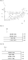
- the display module 100 may have a structure in which a display panel 140, a touch panel 130, an antenna layer 120, and a window cover 110 are stacked in this order.
- the layered structure of the display module 100 is not limited to the structure shown in FIG.
- a display module 100-1 may have a structure in which a display panel 140, an antenna layer 120, a touch panel 130, and a window cover 110 are stacked in the order as shown in FIG. 3B .
- the display module 100 has the structure shown in FIG. 3A .
- the window cover 110 may be provided to protect the display module 100.
- the window cover 110 may be made of a transparent material with predetermined transmittance.
- the window cover 110 may be made of glass or a transparent plastic material having a uniform thickness and transmittance of a predetermined degree or more.
- the window cover 110 may be tempered glass or thin-film glass into which a protection film is laminated.
- the window cover 110 may be a resin film.
- the window cover 110 may be made of polyethyleneTerephthalate (PET), polymethylmethacrylate (PMMA), acryl, polycarbonate (PC), polyimide (PI), polyethylene naphthalate (PEN), triacetate cellulose (TAC), polyether sulfone (PES), or the like.
- the window cover 110 is a resin film having flexibility
- a thin, light-weight display module 100 can be implemented.
- the display module 100 can be freely bent or flexed so that it can be applied to various kinds of devices based on design freedom.
- the antenna layer 120 which is provided to ensure transmission and reception performance of the electronic device 1, may be below the window cover 110.
- the antenna layer 120 may have a metal mesh structure in order to ensure visibility of the display module 100.
- One surface of the antenna layer 120 on which a mesh pattern is formed may be toward the front surface of the display module 100. According to an embodiment of the present disclosure, one surface of the antenna layer 120 on which a mesh pattern is formed may be toward the back surface of the display module 100.
- one surface of the electronic device 1 on which images are displayed is defined as a front surface
- the other surface of the electronic device 1 is defined as a back surface.
- the visibility and conductivity of the display module 100 may depend on how the mesh pattern of the antenna layer 120 is formed. Also, the conductivity of the display module 100 may depend on a kind of a conductive ink used to form the antenna layer 120. This will be described in more detail, later.
- the touch panel 130 may be used to receive touch commands input from a user.
- the touch panel 130 may be below the antenna layer 120.
- the position of the touch panel 130 is not limited to this.
- one surface of the touch panel 130 may be coupled with an electronic writing sheet (for example, a digitizer).
- the display panel 140 which is provided to display images, may be below the touch panel 130.
- the display panel 140 may be at least one of a Liquid Crystal Display (LCD), a reflective display, an E-ink display, a Passive Matrix Organic Light Emitting Diode (PM OLED) display, and an Active Matrix Organic Light Emitting Diode (AM OLED) display.
- LCD Liquid Crystal Display
- PM OLED Passive Matrix Organic Light Emitting Diode
- AM OLED Active Matrix Organic Light Emitting Diode
- the housing 6 may include a bracket, a back case, and a battery cover.
- the bracket may include an upper bracket and a lower bracket, and the lower bracket may be fixed at the lower part of the upper bracket.
- the bracket may be a mounting plate to fix and support a plurality of electronic components (for example, a communication module, a memory, a processor, an audio device, a speaker, a microphone, and the like).
- the back case may be coupled with the bracket.
- the back case may be separated from the battery cover, or integrated into the battery cover.
- the battery cover may be coupled with the back case to form the back of the electronic device 1.
- the battery cover may include a plurality of hooks at its edges, which are fastened with a plurality of hook fastening grooves of the back case.
- the main circuit board 7 may include a substrate on which a fundamental circuit and a plurality of electronic components are mounted.
- the main circuit board 7 may set an execution environment of the electronic device 1, and enable the electronic device 1 to stably operate.
- the main circuit board 7 may be electrically connected to the display module 100 to control the display module 100.
- the basic structure of the display module 100 has been described above.
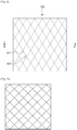
- FIG. 4 shows an example of a mesh pattern formed in the antenna layer 120 according to an embodiment of the present disclosure
- FIG. 5 shows various modifications of the mesh pattern shown in FIG. 4
- FIG. 6 is a cross-sectional view of the antenna layer 120 shown in FIG. 4 , cut along a line B-B'.
- the antenna layer 120 may be formed in a mesh pattern.
- the display module 100 may include the antenna layer 120 formed in the mesh pattern in order to ensure visibility.
- the mesh pattern may be, as shown in FIG. 4 , a pattern in which a plurality of diamond- or square-shaped patterns are uniformly arranged, wherein when ⁇ 1 ⁇ 2, 1° ⁇ 1 ⁇ 89° in order to provide an optimal angle allowing Moire avoidance according to display characteristics.
- the mesh pattern is not limited to the pattern shown in FIG. 4 , and various modifications are possible.
- the mesh pattern may be a pattern in which a plurality of square-shaped patterns are uniformly arranged, as shown in FIG. 5A , a pattern in which a plurality of square- or rectangle-shaped patterns are uniformly arranged, as shown in FIG. 5B , a pattern in which a plurality of hexagon-shaped patterns are uniformly arranged, as shown in FIG. 5C , or a non-uniform pattern in which a plurality of random polygon shapes are arranged, as shown in FIG. 5D .
- the mesh pattern is assumed to be the pattern shown in FIG. 4 .
- the antenna layer 120 may include a substrate 121, and a resin layer 122 formed by an imprinting method.
- the resin layer 122 may include, in its one surface, a plurality of engraved patterns, or groove, 123 (123 for each) and an ink layer 124 formed by filling a conductive material in the engraved patterns 123.
- the engraved patterns 123 may be formed in a mesh pattern as described above, and accordingly, the ink layer 124 may also be formed in a mesh pattern to correspond to the engraved patterns 123.
- the ink layer 124 may function as an electrode structure because it is formed with a conductive material. The conductive material will be described later.
- the transmission and reception performance of the antenna layer 120 included in the display module 100 may depend on a structure of the engraved patterns 123 formed in the substrate 121, more specifically, the ink layer 124 formed to correspond to the engraved patterns 123.
- the antenna layer 120 may have better transmission and reception performance.
- intervals between the engraved patterns 123 that is, the lengths of pitches are shorter, the transmission and reception performance of the antenna layer 120 may be improved.
- the width, depth, and pitch of the engraved patterns 123 are adjusted appropriately.
- FIG. 7 is a view for describing a relationship between the shape of the mesh pattern and transmission and reception performance of the antenna layer 120.
- the width of an engraved pattern 123 is defined as a width W
- the thickness of an engraved pattern 123 is defined as a depth D
- an interval between two neighboring engraved patterns 123 is defined as a pitch P.
- an interval between pattern groups under the different pattern regulations is defined as a pitch
- a straight distance between two neighboring patterns is defined as a pitch.
- a height to width ratio is defined as an aspect ratio.
- an aspect ratio is high, it is possible to improve conductivity due to an increase of the cross-sectional areas of conductors, while minimizing a reduction rate of visibility of the display.
- an aspect ratio is excessively high, it may be difficult to ensure visibility due to a poor viewing angle. Accordingly, an aspect ratio is appropriately adjusted in consideration of both visibility and conductivity.
- Each pattern included in the antenna layer 120 may have a width in a range of approximately 1 ⁇ m to approximately 10 ⁇ m. Generally, if the width of a pattern is below 1.8 ⁇ m, it is difficult to recognize the pattern with a human's naked eyes. Accordingly, by reducing the widths of the patterns, visibility of the display module 100 can be improved. However, if the widths of the patterns are excessively reduced, the metal mesh structure may fail to ensure conductivity due to a decrease of the cross-sectional areas of the conductors. Accordingly, a lower limit on the widths of the patterns may be set to 1 ⁇ m or more.
- an advantage may be acquired in view of conductivity of the ink layer 124, which may lead to ensuring transmission and reception performance of the antenna layer 120.
- an upper limit on the widths of the patterns may be set to 10 ⁇ m or less.
- Each pattern may have a depth in a range of approximately 1 ⁇ m to approximately 18.5 ⁇ m.
- a depth to width ratio of a pattern is great, an advantage can be obtained in view of visibility. For example, comparing a case in which the width of a pattern is 2 ⁇ m and the depth of the pattern is 4 ⁇ m to a case in which the width of a pattern is 4 ⁇ m and the depth of the pattern is 2 ⁇ m, the former case shows higher visibility than the latter case, while the two cases show the same conductivity. This is because a pattern area that a human's naked eyes can recognize is small. Accordingly, the depths of patterns may be adjusted in consideration of the widths of the patterns.
- the depths of the patterns may be set to 18.5 ⁇ m or less.
- the patterns may have a pitch in a range of approximately 50 ⁇ m to approximately 250 ⁇ m. If the length of the pitch is short, a density of metal per unit area may increase to improve conductivity of the electrode structure. However, if the length of the pitch is excessively short, visibility may deteriorate. Accordingly, a lower limit on the pitch may be set to 50 ⁇ m or more.
- an upper limit on the pitch may be set to 250 ⁇ m or less.
- Resistance values shown in Table 1 are resistance values measured on Samples 1 to 8 each having a size of 4*60mm in which mesh patterns having widths, depths, and pitches as shown in Table 1 are respectively formed.
- the structure of the antenna layer 120 has been described above.
- the antenna layer 120 may be disposed between the window cover 110 and the touch panel 130 of the display module 100. However, the antenna layer 120 of the display module 100 may be disposed at another position than between the window cover 110 and the touch panel 130, according to an embodiment.
- FIG. 8 shows a detailed structure of the display module 100 according to an embodiment of the present disclosure, and various arrangement examples of the antenna layer 120 included in the display module 100.
- the display module 100 may include a window protection coating layer 111 and a plurality of adhesive layers 112 and 113, in addition to the components shown in FIGS. 3A and 3B .
- the window protection coating layer 111 may be formed on the window cover 110 to protect the window cover 110.
- the first and second adhesive layers 112 and 113 may be disposed between the window cover 110 and the touch panel 130 and between the touch panel 130 and the display panel 140, respectively.
- the first and second adhesive layers 112 and 113 may be provided between the individual layers to facilitate attachment of the layers while isolating the layers.
- the first and second adhesive layers 112 and 113 may include an Optical Clear Adhesive (OCA) film, although the disclosure is not limited to this.
- OCA Optical Clear Adhesive
- the antenna layer 120 may be disposed between the individual layers shown in FIG. 8 . More specifically, the antenna layer 120 may be disposed between the window protection coating layer 111 and the window cover 110 (P1), between the window cover 110 and the first adhesive layer 112 (P2), between the first adhesive layer 112 and the touch panel 130 (P3), between the touch panel 130 and the second adhesive layer 113 (P4), or between the second adhesive layer 113 and the display panel 140 (P5).
- the display panel 140 may include a polarizing film 141 and an organic light emitting layer 142.
- the antenna layer 120 may be also disposed between the polarizing film 141 and the organic light emitting layer 142 (P6).
- the antenna layer 120 When the antenna layer 120 is disposed at each position PI to P6, the antenna layer 120 may be positioned such that the mesh pattern formed on one surface of the substrate is toward the front or back surface of the display module 100.
- the antenna layer 120 may be provided as a separate layer, as described above with reference to FIGS. 1 to 6 . However, according to an embodiment, the antenna layer 120 may be formed directly on one surface of a component that is basically provided to the display module 100. For example, a conductive ink may be coated on one surface of the window cover 110 to provide a conductive pattern in the form of a thin film without having to insert any additional component, which may contribute to slimming of the electronic device 1.
- a layered structure of a display module according to an embodiment of the present disclosure will be described with reference to the appended drawings.
- FIG. 9 shows a layered structure of a display module according to a present invention.
- a display module 100a includes a window cover 110a, an antenna layer 120a, a touch panel 130a, and a display panel 140a.
- the window cover 110a, the touch panel 130a, and the display panel 140a may be substantially the same as the window cover 110, the touch panel 130, and the display panel 140 shown in FIGS. 3A and 3B , and accordingly, further descriptions thereof will be omitted.
- the antenna layer 120a is formed in a mesh pattern, like the antenna layer 120 shown in FIGS. 4 and 5 , by an imprinting method. More specifically, the antenna layer 120a is formed directly on one surface of the window cover 110a, which may lead to slimming of the display module 100a.
- the antenna layer 120a may be formed on a layer other than the window cover 110a.
- FIG. 10 shows a detailed structure of the display module 100a according to an embodiment of the present disclosure, and various formation examples of the antenna layer 120a included in the display module 100a.
- the display module 100a may include a window protection coating layer 111a and a plurality of adhesive layers (that is, a first adhesive layer 112a and a second adhesive layer 113a), in addition to the components shown in FIG. 9 . More specifically, the display module 100a may have a structure in which the display panel 140a, the second adhesive layer 113a, the touch panel 130a, the first adhesive layer 112a, the window cover 110a, and the window protecting coating layer 111a are stacked in this order.
- the antenna layer 120a may be formed on one surface of each layer shown in FIG. 10 . More specifically, the antenna layer 120a may be formed on the rear surface of the window protection coating layer 111a (P1), on the front surface of the window cover 110a (P2), on the rear surface of the window cover 110a (P3), on the front surface of the touch panel 130a (P6), on the rear surface of the touch panel 130a (P7), or on the front surface of the display panel 140a (P10).
- the display panel 140a may include a polarizing film 141a and an organic light emitting layer 142a.
- the antenna layer 120a may be also formed on one surface of the polarizing film 141a or the organic light emitting layer 142a (P11 and P12).
- the antenna layer 120 or 120a may be formed with a transparent, conductive material in order to ensure visibility of the display module 100 or 100a.
- the transparent, conductive material may be a conductive ink having low resistance in order to ensure transmission and reception performance of an antenna.
- Transparency and transmission and reception performance of the antenna layer 120 or 120a may depend on a mixing proportion of the conductive ink used to form the antenna layer 120 or 120a, a kind of conductive particles included in the conductive ink, etc.
- the conductive ink used to form the antenna layer 120 or 120a will be described in detail.
- the conductive ink according to an embodiment of the present disclosure may contain the same kind of conductive particles.
- the same kind of conductive particles may have the same size.
- the same kind of conductive particles may have different sizes and shapes.
- FIG. 11 shows an example in which conductive particles of the same size are provided
- FIG. 12 shows an example in which conductive particles of different sizes are provided
- FIG. 13 shows an example in which conductive particles of different sizes and shapes are provided.
- FIGS. 11 , 12, and 13 the left drawings show states in which a conductive ink is filled in an engraved pattern 123, and the right drawings show states in which conductive particles are connected due to heat generated by post-processing of applying heat, light, or pressure to the conductive ink, or due to heat generated by resistance of the conductive particles when power is supplied to the conductive particles.
- the conductive ink may contain conductive particles of the same size.
- the conductive ink according to the current embodiment may contain conductive particles of the same size.
- the conductive particles may melt at different temperatures according to their sizes. Because the conductive ink according to the current embodiment contains conductive particles of the same size, it is easy to adjust a melting temperature of the conductive particles. Accordingly, if the conductive ink according to the current embodiment is used in a process of manufacturing the antenna layer 120 or 120a, it may be easy to adjust a melting temperature of the conductive ink when the conductive ink was hardened.
- the conductive ink may contain first particles D1 and second particles D2, wherein the size of the first particles D1 may be different from that of the second particles D2. More specifically, a mean particle size of the first particles D1 may be greater than that of the second particles D2. According to an embodiment, a mean particle size of the first particles D1 may be 1 to 1500 times greater than that of the second particles D2. However, the mean particle sizes of the first particles D1 and the second particle D2 are not limited to the above-mentioned value range.
- the conductive ink may have different mean particle sizes per unit distance.
- the conductive ink can be filled with high density in a target area (for example, in the engraved pattern 123).
- the first particles D1 having the greater mean particle size per unit distance electrical contact resistance may be reduced, and as a result, conductivity of the antenna layer 120 or 120a may be improved due to an ink layer 124 resulting from hardening of the conductive ink.
- the second particles D2 having the smaller size may be filled between the first particles D1 having the greater size to increase density of metal.
- first and second particles D1 and D2 may have nano sizes.
- the sizes and shapes of the first and second particles D1 and D2 are not limited to nano sizes, and the first and second particles D1 and D2 may have sizes of several hundreds of picometers to several hundreds of micrometers.
- the conductive ink may contain third particles D3 and fourth particles D4, wherein the shape of the third particles D3 may be different from that of the fourth particles D4.
- the third particles D3 may be in the shape of nano dots
- the fourth particles D4 may be in the shape of nano rods.
- the nano rods may allow electrical conduction to a relatively long distance due to a high aspect ratio. Accordingly, contact resistance at contact areas between the particles may be reduced, and as a result, conductivity of the antenna layer 120 or 120a can be improved by the ink layer 124 resulting from hardening of the conductive ink.
- the conductive ink may contain conductive particles in the shape of nano dots, and a metallic complex compound.
- the metallic complex compound may resolve into a metal to surround the nano dots, which reduces contact resistance between the nano dots to thereby improve conductivity.
- the conductive particles may include particles for low temperature and particles for high temperature. More specifically, the particles for low temperature may be at least one selected from a group including silver (Ag), copper (Cu), and Nickel (Ni), and the particles for high temperature may be at least one selected from a group including a silver (Ag)-lead (Pb) alloy, gold (Au), a gold (Au)-platinum (Pt) alloy, a gold (Au)-lead (Pb) alloy, a copper (Cu)-Nickel (Ni) alloy, and tungsten (W).
- the conductive particles are not limited to the above-mentioned examples.
- the antenna layer 120 or 120a is formed with a polished metal material, light incident from the outside or image light output from the display panel may be reflected from the antenna layer 120 or 120a, which may deteriorate a contrast ratio.
- a blackened layer may be formed on the surface of the antenna layer 120 or 120a in order to suppress reflection of light incident from the outside.
- the blackened layer may be formed by including a blackening material in a conductive ink provided to form the antenna layer 120 or 120a.
- a blackening material is included in a conductive ink will be described in detail.
- the conductive ink according to an embodiment of the present disclosure may further include a blackened material, in addition to the conductive particles described above.
- the blackened material may be added in powder form in the conductive ink.
- the blackened material added in powder form will be referred to as blackened particles.
- the conductive ink may include approximately 10 to approximately 75 parts of weight of a solvent and approximately 25 to approximately 90 parts of weight of a solid with respect to the entire weight of the conductive ink, and the solid may include approximately 80 to approximately 99 parts of weight of conductive particles and approximately 1 to approximately 20 parts of weight of blackened particles with respect to the entire weight of the solid.
- the conductive ink may include approximately 10 to approximately 75 parts of weight of a solvent, approximately 40 to approximately 89.1 parts of weight of conductive particles, and approximately 0.5 to approximately 18 parts of weight of blackened particles with respect to the entire weight of the conductive ink.
- the conductive particles may include, as described above, particles for low temperature and particles for high temperature. Hereinafter, repetitive descriptions about the kinds of the conductive particles will be omitted.
- the blackened particles may be at least one selected from a group including carbon black, graphite, carbon nanotube, polyacetylene, polypyrrole, polyaniline, and polythiophene.
- the blackened particles may be included at an appropriate proportion in the conductive ink. More specifically, if a small amount of the blackened material is included in the conductive ink, light incident from the outside may be reflected from the surface of the antenna layer 120 or 120a, which may make ensuring visibility difficult. Meanwhile, if a large amount of the blackened material is included in the conductive ink, a proportion of the conductive particles in the conductive ink may be relatively lowered, which may make ensuring conductivity difficult. Accordingly, a proportion of the blackened material is appropriately adjusted in the conductive ink.
- the blackened particles may have a lower specific gravity than the conductive particles.
- the blackened particles may be graphite particles having a specific gravity of approximately 1.6.
- the conductive particles may be silver (Ag) particles having a specific gravity of approximately 10.49, gold (Au) particles having a specific gravity of approximately 19.29, lead (Pb) particles having a specific gravity of approximately 11.34, copper (Cu) particles having a specific gravity of approximately 8.93, nickel (Ni) particles having a specific gravity of approximately 8.9, or platinum (Pt) particles having a specific gravity of approximately 21.45.
- a density of the conductive particles may be within a range of approximately 0.1 to approximately 20g/cm 3 , and may be within a range of approximately 2.7 to approximately 20g/cm 3 .
- a density of the blackened particles may be within a range of approximately 0.1 to approximately 1.5 g/cm 3 .
- a blackened layer may be formed on the surface of the ink layer 124 due to a specific gravity difference between the conductive particles and the blackened particles.
- FIG. 14 is a view for describing a blackening process according to an embodiment of the present disclosure.
- the conductive particles D having a relatively high specific gravity may sink to the lower part of the engraved pattern 123 by gravity, and the blackened particles B having a relatively low specific gravity may float on the upper part of the engraved pattern 123.
- the blackened particles B positioned above the conductive particles D may be hardened to form the blackened layer 125 on the surface of an ink layer 125.
- the surface of the antenna layer 120 or 120a can be blackened by a single process.
- the blackened particles B and the conductive particles D may have the same size. However, according to an embodiment, the blackened particles B and the conductive particles D may have different sizes. Also, the conductive particles D may have the same size or different sizes.
- repetitive descriptions about those described above with reference to FIGS. 11 to 13 will be omitted.
- the conductive ink may further include a binder and an additive.
- the binder may be used to facilitate close contacts between the conductive particles D.
- the binder may be at least one selected from a group including phenol, acryl, urethane, epoxy, melamine, glass frit, and fluorosilicate. More specifically, if conductive particles for low temperature are a main part of the conductive ink, a binder, such as phenol, acryl, urethane, epoxy, and melamine, may be used, and if conductive particles for high temperature are a main part of the conductive ink, a binder, such as glass frit and fluorosilicate, may be used.
- the additive may be added to disperse particles or improve printing quality.
- the additive may be at least one selected from a group including 4000 series of EFKA, Disprebyk series of BYK, Solsperse series of Avecia, TEGO Disperse series of Deguessa, Disperse-AYD series of Elementis, JONCRYL series of Johnson Polymer, Ethyl Cellulose, and Acryl.
- the additive is not limited to the above-mentioned materials.
- FIG. 15 is a flowchart illustrating a method of manufacturing a display module according to an embodiment of the present disclosure
- FIG. 16 is a schematic view for describing the manufacturing method of FIG. 15 .
- the display module includes a first panel and a second panel, and the antenna layer 120a is formed on one surface of the first panel (see the structure of the display module 100a shown in FIGS. 9 and 10 ), a method of manufacturing the display module 100a will be described.
- the method of manufacturing the display module 100a may include operation 200 of forming the antenna layer 120a on one surface of the first panel by an imprinting method, and operation 250 of coupling the first panel with the second panel.
- the first panel and the second panel may include the window cover 110a, the touch panel 130a, and the display panel 140a.
- the first panel and the second panel may include, in addition to the window cover 110a, the touch panel 130a, and the display panel 140a, a separate substrate (for example, the window protection coating layer 111a, the polarizing layer 141a of the display panel 140a, or the organic light emitting layer 142a) or an adhesive layer 112a or 113a for making the above-mentioned panels adhere to each other.
- a separate substrate for example, the window protection coating layer 111a, the polarizing layer 141a of the display panel 140a, or the organic light emitting layer 142a
- an adhesive layer 112a or 113a for making the above-mentioned panels adhere to each other.
- the first panel is assumed to be the window cover 110a
- the second panel is assumed to be the display panel 140a.
- Operation 200 of forming the antenna layer 120a on one surface of the first panel 110a by the imprinting method may include operation 210 of applying a resin 114 on the first panel 110a, operation 220 of pressing the applied resin 114 with a hard stamp 115 and then hardening the resin 114 to form an engraved pattern 123, operation 230 of applying a conductive ink in the engraved pattern 123, and operation 240 of hardening the conductive ink.
- Operation 210 of applying the resin 114 on one surface of the first panel 110a may include applying the resin 114 on one surface of the window cover 110a.
- the window cover 110a may be a transparent window cover having a predetermined transmittance.
- the window cover 110a may be glass having a uniform thickness and transmittance of a predetermined degree or more.
- repetitive descriptions about the window cover 110a as described above with reference to FIG. 3 will be omitted.
- the resin 114 may be a UV resin having predetermined viscosity, or a transparent, thermosetting resin.
- a resin layer 114a having a uniform height and thickness may be formed.
- no additional member for forming the antenna layer 120a may be needed, which may lead to slimming of the electronic device 1.
- the applied resin 114 may be pressed with the hard stamp 115 to form the engraved pattern 123 (operation 220).
- the hard stamp 115 may be made of a polydimethylsiloxane (PDMS) material.
- PDMS polydimethylsiloxane
- a micropattern may be formed.
- the engraved pattern 123 may be in the form of a mesh pattern.
- the mesh pattern may be formed to correspond to the engraved pattern 123, and the mesh pattern may have a width of approximately 1 to approximately 10 ⁇ m, a depth of approximately 1 to approximately 18.5 ⁇ m, and a pitch of approximately 50 to approximately 250 ⁇ m. Accordingly, the engraved pattern 123 may be formed to be greater than the mesh pattern such that the mesh pattern has such a shape as described above.
- operation 230 of applying a conductive ink in the engraved pattern 123 may be performed.
- the conductive ink having predetermined transmittance and conductivity may be filled in the engraved pattern 123 to form an electrode pattern corresponding to the engraved pattern 123.
- the conductive ink may contain the same kind of conductive particles.
- the conductive particles may have the same size, or may have different sizes or shapes according to an embodiment. Hereinafter, repetitive descriptions about the conductive particles will be omitted.
- the conductive particles may include particles for low temperature and particles for high temperature. More specifically, the particles for low temperature may be at least one selected from a group including silver (Ag), copper (Cu), and Nickel (Ni), and the particles for high temperature may be at least one selected from a group including a silver (Ag)-lead (Pb) alloy, gold (Au), a gold (Au)-platinum (Pt) alloy, a gold (Au)-lead (Pb) alloy, a copper (Cu)-Nickel (Ni) alloy, and tungsten (W).
- the conductive particles are not limited to the above-mentioned examples.
- an electrode pattern may be formed on one surface of the window cover 110a, and the electrode pattern may function as the antenna layer 120a.
- the second panel 140a may be the display panel 140a as described above. More specifically, the second panel 140a may be at least one of LCD, a reflective display, an E-ink display, a PM OLED display, and an AM OLED display. However, the display panel 140a is not limited to the above-mentioned displays.
Landscapes
- Engineering & Computer Science (AREA)
- Theoretical Computer Science (AREA)
- Computer Hardware Design (AREA)
- Physics & Mathematics (AREA)
- General Physics & Mathematics (AREA)
- General Engineering & Computer Science (AREA)
- Human Computer Interaction (AREA)
- Chemical & Material Sciences (AREA)
- Computer Networks & Wireless Communication (AREA)
- Organic Chemistry (AREA)
- Materials Engineering (AREA)
- Life Sciences & Earth Sciences (AREA)
- Wood Science & Technology (AREA)
- Chemical Kinetics & Catalysis (AREA)
- General Chemical & Material Sciences (AREA)
- Composite Materials (AREA)
- Devices For Indicating Variable Information By Combining Individual Elements (AREA)
- Details Of Aerials (AREA)
- Support Of Aerials (AREA)
- Microelectronics & Electronic Packaging (AREA)
- Inorganic Chemistry (AREA)
- Nanotechnology (AREA)
- General Life Sciences & Earth Sciences (AREA)
- Geology (AREA)
Claims (10)
- Anzeigemodul (100a), das Folgendes umfasst:eine Fensterabdeckung (110a);eine Antennenschicht (120a), die auf einer Oberfläche der Fensterabdeckung (110a) mittels eines Eindruckverfahrens gebildet wird und eine Harzschicht (114a) beinhaltet;ein Bedienfeld (130a), das an der Fensterabdeckung (110a) so angebracht wird, dass die Antennenschicht (120a) zwischen der Fensterabdeckung (110a) und dem Bedienfeld (130a) angeordnet ist; undein Anzeigefeld (140a), das an dem Bedienfeld (130a) angebracht wird,wobei die Harzschicht (114a) Folgendes beinhaltet:eine Vielzahl von Rillen (123), die in einer Oberfläche der Harzschicht (114a) gebildet werden, undeine leitfähige Farbe (124), die in die Vielzahl von Rillen (123) gefüllt wird,wobei die Vielzahl von Rillen (123) ein Gittermuster bilden.
- Anzeigemodul gemäß Anspruch 1, wobei das Gittermuster eine Breite von 1 µm bis 10 µm, eine Tiefe von 1 µm bis 18,5 µm und ein Musterintervall von 50 µm bis 250 µm aufweist.
- Anzeigemodul gemäß Anspruch 1, wobei die Antennenschicht (120a) transparent ist.
- Anzeigemodul gemäß Anspruch 1, wobei die Harzschicht (114a) durch Auftragen eines Harzes (114) auf die Fensterabdeckung (110a), Pressen des aufgetragenen Harzes, um die Vielzahl von Rillen (123) zu bilden, und Auftragen der leitfähigen Farbe (124) in die Vielzahl von Rillen (123) gebildet wird.
- Anzeigemodul gemäß Anspruch 1, wobei
die leitfähige Farbe (124) leitfähige Teilchen enthält und
ein wesentlicher Teil der leitfähigen Teilchen mindestens eines von der gleichen Größe, der gleichen Form und des gleichen Materials ist oder wobei ein wesentlicher Teil der leitfähigen Teilchen mindestens eines von unterschiedlichen Größen und unterschiedlichen Formen aufweist. - Anzeigemodul gemäß Anspruch 1, wobei die leitfähige Farbe (124) leitfähige Teilchen enthält, die mindestens eines beinhalten, das aus einer Gruppe ausgewählt ist, die Silber (Ag), Kupfer (Cu), Nickel (Ni), eine Silber(Ag)-Blei(Pb)-Legierung, Gold (Au), eine Gold(Au)-Platin(Pt)-Legierung, eine Kupfer(Cu)-Nickel(Ni)-Legierung und Wolfram (W) beinhaltet.
- Anzeigemodul gemäß Anspruch 5, wobei die leitfähige Farbe (124) ferner geschwärzte Teilchen enthält.
- Anzeigemodul gemäß Anspruch 7, wobei die geschwärzten Teilchen ein niedrigeres spezifisches Gewicht als die leitfähigen Teilchen aufweisen.
- Anzeigemodul gemäß Anspruch 7, wobei die geschwärzten Teilchen mindestens eines beinhalten, das aus einer Gruppe ausgewählt ist, die Industrieruß, Graphit, Kohlenstoffnanoröhre, Polyacetylen, Polypyrrol, Polyanilin und Polythiophen beinhaltet.
- Anzeigemodul gemäß Anspruch 1, wobei das Anzeigefeld (140a) mindestens eines von einer Flüssigkristallanzeige (Liquid Crystal Display, LCD), einer reflektierenden Anzeige, einer E-Ink-Anzeige, einer Passiv-Matrix-Anzeige mit organischer Leuchtdiode (PM-OLED-Anzeige, PM-OLED = Passive Matrix Organic Light Emitting Diode) und einer Aktiv-Matrix-Anzeige mit organischer Leuchtdiode (AM-OLED-Anzeige, AM-OLED = Active Matrix Organic Light Emitting Diode Display) beinhaltet.
Priority Applications (1)
| Application Number | Priority Date | Filing Date | Title |
|---|---|---|---|
| EP20213224.7A EP3809244B1 (de) | 2015-05-22 | 2015-12-17 | Anzeigemodul und verfahren zur herstellung davon |
Applications Claiming Priority (3)
| Application Number | Priority Date | Filing Date | Title |
|---|---|---|---|
| US201562165279P | 2015-05-22 | 2015-05-22 | |
| KR1020150138949A KR102399741B1 (ko) | 2015-05-22 | 2015-10-02 | 디스플레이 모듈 및 그 제조 방법 |
| PCT/KR2015/013848 WO2016190506A1 (en) | 2015-05-22 | 2015-12-17 | Display module and method of manufacturing the same |
Related Child Applications (1)
| Application Number | Title | Priority Date | Filing Date |
|---|---|---|---|
| EP20213224.7A Division EP3809244B1 (de) | 2015-05-22 | 2015-12-17 | Anzeigemodul und verfahren zur herstellung davon |
Publications (3)
| Publication Number | Publication Date |
|---|---|
| EP3298480A1 EP3298480A1 (de) | 2018-03-28 |
| EP3298480A4 EP3298480A4 (de) | 2018-05-30 |
| EP3298480B1 true EP3298480B1 (de) | 2020-12-16 |
Family
ID=57707277
Family Applications (2)
| Application Number | Title | Priority Date | Filing Date |
|---|---|---|---|
| EP20213224.7A Active EP3809244B1 (de) | 2015-05-22 | 2015-12-17 | Anzeigemodul und verfahren zur herstellung davon |
| EP15893458.8A Active EP3298480B1 (de) | 2015-05-22 | 2015-12-17 | Anzeigemodul und verfahren zur herstellung davon |
Family Applications Before (1)
| Application Number | Title | Priority Date | Filing Date |
|---|---|---|---|
| EP20213224.7A Active EP3809244B1 (de) | 2015-05-22 | 2015-12-17 | Anzeigemodul und verfahren zur herstellung davon |
Country Status (7)
| Country | Link |
|---|---|
| US (2) | US10573955B2 (de) |
| EP (2) | EP3809244B1 (de) |
| JP (1) | JP6744334B2 (de) |
| KR (2) | KR102399741B1 (de) |
| CN (1) | CN107646095B (de) |
| AU (1) | AU2015396104B2 (de) |
| WO (1) | WO2016190506A1 (de) |
Families Citing this family (50)
| Publication number | Priority date | Publication date | Assignee | Title |
|---|---|---|---|---|
| US9813102B2 (en) | 2014-12-15 | 2017-11-07 | Intel Corporation | Display panel with transparent conductor based isolator and method for improved wireless communications |
| CN106299148B (zh) * | 2015-06-10 | 2018-04-03 | 上海和辉光电有限公司 | 显示面板的封装结构及封装方法 |
| CN105094231B (zh) * | 2015-07-28 | 2019-03-01 | 京东方科技集团股份有限公司 | 一种显示屏和便携设备 |
| JP2019053343A (ja) * | 2016-01-29 | 2019-04-04 | シャープ株式会社 | アンテナ内蔵タッチパネル |
| KR102666192B1 (ko) * | 2016-07-28 | 2024-05-14 | 삼성디스플레이 주식회사 | 표시 장치 |
| CN108574141B (zh) * | 2017-03-16 | 2021-08-20 | 富士康(昆山)电脑接插件有限公司 | 电子设备及其具有lds天线的基板以及基板制作方法 |
| KR102426365B1 (ko) * | 2017-08-21 | 2022-07-29 | 삼성전자 주식회사 | 안테나를 포함하는 전자 장치 |
| US10249944B1 (en) * | 2017-09-25 | 2019-04-02 | Antwave Intellectual Property Limited | Systems, apparatus, and methods to improve antenna performance in electronic devices |
| CN109992043A (zh) * | 2017-12-29 | 2019-07-09 | 南昌欧菲显示科技有限公司 | 装饰膜和电子装置 |
| KR101962819B1 (ko) | 2018-03-06 | 2019-03-27 | 동우 화인켐 주식회사 | 안테나가 결합된 화상 표시 장치 및 화상 표시 장치용 안테나 |
| CN108512959B (zh) * | 2018-03-28 | 2020-08-14 | Oppo广东移动通信有限公司 | 电子设备及存储介质 |
| US20190355277A1 (en) | 2018-05-18 | 2019-11-21 | Aidmics Biotechnology (Hk) Co., Limited | Hand-made circuit board |
| CN108963423B (zh) * | 2018-07-12 | 2020-11-10 | 宇龙计算机通信科技(深圳)有限公司 | 天线结构及具有所述天线结构的穿戴式电子装置 |
| KR102455588B1 (ko) * | 2018-12-06 | 2022-10-14 | 동우 화인켐 주식회사 | 안테나 구조체 및 이를 포함하는 디스플레이 장치 |
| KR102551690B1 (ko) * | 2018-12-06 | 2023-07-05 | 삼성전자주식회사 | 접착 구조를 포함하는 전자 장치 |
| US20200192542A1 (en) * | 2018-12-12 | 2020-06-18 | Novatek Microelectronics Corp. | Display device with integrated antenna and method thereof |
| WO2020131643A1 (en) | 2018-12-18 | 2020-06-25 | Patriotis Marios | The achievement of close to pure wideband circular polarization in printed antenna arrays |
| CN110048224B (zh) * | 2019-03-28 | 2021-05-11 | Oppo广东移动通信有限公司 | 天线模组和电子设备 |
| JP6902064B2 (ja) * | 2019-04-17 | 2021-07-14 | Nissha株式会社 | ディスプレイ装置 |
| CN112306273A (zh) * | 2019-07-26 | 2021-02-02 | 北京小米移动软件有限公司 | 触控显示屏和移动终端 |
| CN112635980A (zh) * | 2019-09-24 | 2021-04-09 | 北京小米移动软件有限公司 | 透光薄膜天线及具有该透光薄膜天线的移动通信终端 |
| CN110534881B (zh) * | 2019-09-25 | 2021-01-22 | 京东方科技集团股份有限公司 | 液晶天线及其制作方法 |
| KR102756487B1 (ko) * | 2019-10-31 | 2025-01-21 | 삼성디스플레이 주식회사 | 무선 주파수 소자 및 이를 포함하는 전자 장치 |
| CN112928438B (zh) * | 2019-11-20 | 2023-10-20 | 华为技术有限公司 | 盖板及电子设备 |
| KR102241964B1 (ko) * | 2019-12-05 | 2021-04-16 | 동우 화인켐 주식회사 | 안테나 소자 및 이를 포함하는 디스플레이 장치 |
| CN210984952U (zh) | 2019-12-06 | 2020-07-10 | 昇印光电(昆山)股份有限公司 | 一种透明天线 |
| US11237412B1 (en) * | 2019-12-17 | 2022-02-01 | Snap Inc. | Antenna implementation embedded in optical waveguide module |
| KR102637667B1 (ko) * | 2019-12-23 | 2024-02-19 | 엘지이노텍 주식회사 | 투명안테나 및 이를 포함하는 안테나 장치 |
| CN111129743A (zh) * | 2020-01-13 | 2020-05-08 | 隽美经纬电路有限公司 | 一种透明的柔性天线板及其制作方法 |
| KR20210097342A (ko) | 2020-01-30 | 2021-08-09 | 동우 화인켐 주식회사 | 안테나 소자 및 이를 포함하는 디스플레이 장치 |
| CN113258274B (zh) * | 2020-02-10 | 2025-06-06 | 东友精细化工有限公司 | 天线堆叠结构和包括天线堆叠结构的显示装置 |
| KR102703335B1 (ko) * | 2020-02-28 | 2024-09-04 | 동우 화인켐 주식회사 | 안테나 소자 및 이를 포함하는 디스플레이 장치 |
| US11733744B2 (en) * | 2020-04-28 | 2023-08-22 | Qualcomm Incorporated | Display-side antenna |
| KR102371027B1 (ko) | 2020-04-29 | 2022-03-04 | 동우 화인켐 주식회사 | 안테나 적층체 및 이를 포함하는 디스플레이 장치 |
| US11050144B1 (en) * | 2020-05-08 | 2021-06-29 | W. L. Gore & Associates, Inc. | Assembly with at least one antenna and a thermal insulation component |
| US12174660B2 (en) | 2020-06-11 | 2024-12-24 | Apple Inc. | Electronic device |
| US11592870B2 (en) * | 2020-06-11 | 2023-02-28 | Apple Inc. | Electronic device architecture and components |
| KR102871253B1 (ko) | 2020-06-29 | 2025-10-16 | 삼성전자 주식회사 | 안테나 및 그것을 포함하는 전자 장치 |
| KR102766427B1 (ko) * | 2020-08-28 | 2025-02-12 | 동우 화인켐 주식회사 | 도전성 메쉬 구조체의 및 이를 포함하는 안테나 소자 |
| USD951108S1 (en) * | 2020-09-01 | 2022-05-10 | Garmin Switzerland Gmbh | Watch with display |
| KR20230083307A (ko) * | 2020-10-08 | 2023-06-09 | 다이니폰 인사츠 가부시키가이샤 | 헤드 마운트 디스플레이 |
| USD939499S1 (en) * | 2020-10-22 | 2021-12-28 | Shenzhen Qian Hai Woer Technology Limited. | Smart watch |
| USD929989S1 (en) * | 2020-10-28 | 2021-09-07 | Shenzhen Starmax Technology Co., Ltd | Smart watch |
| CN113472923B (zh) * | 2021-06-25 | 2024-05-10 | 安徽精卓光显技术有限责任公司 | 一种带透明天线的手机后盖及其制备方法 |
| USD963639S1 (en) * | 2021-07-23 | 2022-09-13 | Jing Zhang | Smart watch |
| US12230898B2 (en) * | 2021-10-25 | 2025-02-18 | Chasm Advanced Materials, Inc. | Transparent radio frequency antenna and EMI shield |
| US20240097318A1 (en) * | 2022-05-16 | 2024-03-21 | Meta Platforms Technologies, Llc | Transparent antenna and touch display on a wearable device |
| KR20230165984A (ko) | 2022-05-27 | 2023-12-06 | 삼성디스플레이 주식회사 | 편광 필름 및 이를 채용하는 표시 장치 |
| KR20240119937A (ko) | 2023-01-30 | 2024-08-07 | 삼성디스플레이 주식회사 | 표시 장치 및 표시 장치의 제조방법 |
| KR102583971B1 (ko) * | 2023-05-25 | 2023-09-26 | 주식회사 케이앤에스아이앤씨 | 위성안테나용 반사판 및 그 제조방법. |
Citations (1)
| Publication number | Priority date | Publication date | Assignee | Title |
|---|---|---|---|---|
| JP2014212211A (ja) * | 2013-04-18 | 2014-11-13 | 大日本印刷株式会社 | 導電性メッシュ、導電性メッシュシート、タッチパネル装置および画像表示装置 |
Family Cites Families (26)
| Publication number | Priority date | Publication date | Assignee | Title |
|---|---|---|---|---|
| US6786733B2 (en) * | 2002-10-15 | 2004-09-07 | Overseas Diamonds Inc. | Computer-implemented method of and system for teaching an untrained observer to evaluate a gemstone |
| US20100026590A1 (en) * | 2004-07-28 | 2010-02-04 | Kuo-Ching Chiang | Thin film multi-band antenna |
| EP1689020B1 (de) * | 2005-01-28 | 2013-03-20 | Mondi Gronau GmbH | Folie mit aufgedruckter Antenne |
| EP1891171B1 (de) * | 2005-06-17 | 2008-12-24 | Exatec, LLC. | Kunststoffglasursystem mit verbesserter haftung der beschichtung auf der oberfläche |
| JP4331763B2 (ja) * | 2007-01-31 | 2009-09-16 | 株式会社アフィット | 導電性粒子の現像方法 |
| JP5194756B2 (ja) * | 2007-12-11 | 2013-05-08 | 大日本印刷株式会社 | プラズマディスプレイ用前面フィルターおよびこれを用いたプラズマディスプレイ |
| JP5003514B2 (ja) * | 2008-01-29 | 2012-08-15 | 大日本印刷株式会社 | 電磁波シールド部材 |
| JP5636735B2 (ja) * | 2009-09-24 | 2014-12-10 | 大日本印刷株式会社 | 透明アンテナ用エレメント及び透明アンテナ |
| CN102055062A (zh) * | 2009-10-29 | 2011-05-11 | 深圳富泰宏精密工业有限公司 | 电子装置壳体及其制作方法 |
| EP2355241A1 (de) * | 2010-02-02 | 2011-08-10 | Laird Technologies AB | Antennenvorrichtung für eine Funkkommunikationsvorrichtung |
| JP2012089782A (ja) * | 2010-10-22 | 2012-05-10 | Dainippon Printing Co Ltd | 導電性外光遮蔽材、導電性外光遮蔽シート体、画像表示装置前面用フィルタ、および画像表示装置 |
| JP5682464B2 (ja) * | 2011-06-13 | 2015-03-11 | 大日本印刷株式会社 | 透明アンテナ、及び画像表示装置 |
| JP2014529642A (ja) * | 2011-08-12 | 2014-11-13 | スリーエム イノベイティブプロパティズカンパニー | 光学的に透明な導電性接着剤及びそれから製造される物品 |
| KR101806942B1 (ko) * | 2011-09-28 | 2017-12-08 | 삼성전자주식회사 | 휴대단말기의 근거리무선통신 안테나장치 |
| JP2013077601A (ja) * | 2011-09-29 | 2013-04-25 | Panasonic Corp | ディスプレイ装置 |
| KR101982010B1 (ko) * | 2012-03-15 | 2019-05-24 | 주식회사 동진쎄미켐 | 금속-판상의 그라핀 분말 및 이를 포함하는 전자파 차폐용 코팅 조성물 |
| US20140106684A1 (en) * | 2012-10-15 | 2014-04-17 | Qualcomm Mems Technologies, Inc. | Transparent antennas on a display device |
| CN102983410B (zh) * | 2012-11-09 | 2014-03-12 | 深圳光启创新技术有限公司 | 反射阵列天线 |
| KR102077065B1 (ko) * | 2013-02-19 | 2020-02-14 | 삼성디스플레이 주식회사 | 안테나가 구비된 표시장치용 윈도우 부재 및 그 제조 방법 |
| KR102053195B1 (ko) * | 2013-04-01 | 2019-12-06 | 엘지전자 주식회사 | 터치 스크린 패널 |
| JP2015041021A (ja) * | 2013-08-23 | 2015-03-02 | 大日本印刷株式会社 | 表示装置用前面保護板及び表示装置 |
| KR101656452B1 (ko) * | 2013-09-06 | 2016-09-09 | 주식회사 잉크테크 | 전도성 패턴 형성 방법 및 전도성 패턴 |
| WO2015042335A1 (en) * | 2013-09-23 | 2015-03-26 | Apple Inc. | Electronic component embedded in ceramic material |
| JP6204858B2 (ja) * | 2014-03-25 | 2017-09-27 | 富士フイルム株式会社 | タッチパネルモジュールおよび電子機器 |
| WO2016002279A1 (ja) * | 2014-06-30 | 2016-01-07 | 富士フイルム株式会社 | タッチパネル及びその製造方法 |
| CN106575181B (zh) * | 2014-08-14 | 2020-03-24 | Lg伊诺特有限公司 | 触摸窗 |
-
2015
- 2015-10-02 KR KR1020150138949A patent/KR102399741B1/ko active Active
- 2015-12-17 EP EP20213224.7A patent/EP3809244B1/de active Active
- 2015-12-17 WO PCT/KR2015/013848 patent/WO2016190506A1/en not_active Ceased
- 2015-12-17 JP JP2017560776A patent/JP6744334B2/ja not_active Expired - Fee Related
- 2015-12-17 EP EP15893458.8A patent/EP3298480B1/de active Active
- 2015-12-17 CN CN201580080243.3A patent/CN107646095B/zh active Active
- 2015-12-17 AU AU2015396104A patent/AU2015396104B2/en not_active Ceased
- 2015-12-22 US US14/977,900 patent/US10573955B2/en active Active
-
2020
- 2020-02-18 US US16/793,297 patent/US11283157B2/en active Active
-
2022
- 2022-05-13 KR KR1020220059146A patent/KR102523260B1/ko active Active
Patent Citations (1)
| Publication number | Priority date | Publication date | Assignee | Title |
|---|---|---|---|---|
| JP2014212211A (ja) * | 2013-04-18 | 2014-11-13 | 大日本印刷株式会社 | 導電性メッシュ、導電性メッシュシート、タッチパネル装置および画像表示装置 |
Also Published As
| Publication number | Publication date |
|---|---|
| US20200203809A1 (en) | 2020-06-25 |
| AU2015396104A1 (en) | 2017-11-30 |
| JP2018524626A (ja) | 2018-08-30 |
| JP6744334B2 (ja) | 2020-08-19 |
| CA2985167A1 (en) | 2016-12-01 |
| US11283157B2 (en) | 2022-03-22 |
| EP3809244B1 (de) | 2023-03-08 |
| EP3298480A4 (de) | 2018-05-30 |
| US20160344089A1 (en) | 2016-11-24 |
| KR102523260B1 (ko) | 2023-04-20 |
| KR20160137315A (ko) | 2016-11-30 |
| KR20220066033A (ko) | 2022-05-23 |
| KR102399741B1 (ko) | 2022-05-20 |
| CN107646095B (zh) | 2020-12-08 |
| WO2016190506A1 (en) | 2016-12-01 |
| EP3298480A1 (de) | 2018-03-28 |
| CN107646095A (zh) | 2018-01-30 |
| EP3809244A1 (de) | 2021-04-21 |
| US10573955B2 (en) | 2020-02-25 |
| AU2015396104B2 (en) | 2021-01-14 |
Similar Documents
| Publication | Publication Date | Title |
|---|---|---|
| US11283157B2 (en) | Display module and method of manufacturing the same | |
| US11516950B2 (en) | Electronic device comprising display module having stress neutralization layer between flexible substrate and conductive layer | |
| EP3338322B1 (de) | Elektronische vorrichtung | |
| US9285843B2 (en) | Electronic device | |
| US11275460B2 (en) | Display device | |
| US20150124179A1 (en) | Display device and method of manufacturing the same | |
| US20130157022A1 (en) | Transparent panel and method of manufacturing the same | |
| CN108539369B (zh) | 天线组件、天线组件的制作方法及电子设备 | |
| US20190196252A1 (en) | Ultra-thin display assembly with integrated touch functionality | |
| CN108281763B (zh) | 天线组件、中框组件及电子设备 | |
| KR20160002448A (ko) | 안테나 일체형 터치패널 | |
| CN208522831U (zh) | 壳体组件及电子设备 | |
| CA2985167C (en) | Display module and method of manufacturing the same | |
| CN108258395B (zh) | 天线组件、中框组件及电子设备 | |
| US20140353012A1 (en) | Transparent conductive film | |
| US9439302B2 (en) | Transparent conductive film | |
| CN108039573B (zh) | 天线组件以及电子设备 | |
| US20240388003A1 (en) | Antenna array embedded in thinned region of display panel | |
| KR20160029468A (ko) | 터치패널 | |
| CN224123546U (zh) | 一种电连接件以及电子设备 | |
| KR20150017473A (ko) | 터치 스크린 패널 및 이의 제조방법 | |
| JP7083930B2 (ja) | タッチパネル及びタッチデバイス | |
| CN108258413B (zh) | 天线组件、中框组件及电子设备 | |
| WO2021102698A1 (zh) | 触控屏、触控显示器及电子设备 |
Legal Events
| Date | Code | Title | Description |
|---|---|---|---|
| STAA | Information on the status of an ep patent application or granted ep patent |
Free format text: STATUS: THE INTERNATIONAL PUBLICATION HAS BEEN MADE |
|
| PUAI | Public reference made under article 153(3) epc to a published international application that has entered the european phase |
Free format text: ORIGINAL CODE: 0009012 |
|
| STAA | Information on the status of an ep patent application or granted ep patent |
Free format text: STATUS: REQUEST FOR EXAMINATION WAS MADE |
|
| 17P | Request for examination filed |
Effective date: 20171221 |
|
| AK | Designated contracting states |
Kind code of ref document: A1 Designated state(s): AL AT BE BG CH CY CZ DE DK EE ES FI FR GB GR HR HU IE IS IT LI LT LU LV MC MK MT NL NO PL PT RO RS SE SI SK SM TR |
|
| AX | Request for extension of the european patent |
Extension state: BA ME |
|
| A4 | Supplementary search report drawn up and despatched |
Effective date: 20180502 |
|
| RIC1 | Information provided on ipc code assigned before grant |
Ipc: C09C 1/48 20060101ALI20180420BHEP Ipc: G04G 21/04 20130101ALI20180420BHEP Ipc: H01Q 1/36 20060101ALI20180420BHEP Ipc: H01Q 1/27 20060101ALI20180420BHEP Ipc: H01Q 1/24 20060101ALI20180420BHEP Ipc: G06F 3/041 20060101AFI20180420BHEP Ipc: G04G 21/08 20100101ALI20180420BHEP Ipc: G06F 1/16 20060101ALI20180420BHEP Ipc: H01Q 1/44 20060101ALI20180420BHEP |
|
| DAV | Request for validation of the european patent (deleted) | ||
| DAX | Request for extension of the european patent (deleted) | ||
| RIC1 | Information provided on ipc code assigned before grant |
Ipc: H01Q 1/24 20060101ALI20180420BHEP Ipc: G04G 21/04 20130101ALI20180420BHEP Ipc: G06F 3/041 20060101AFI20180420BHEP Ipc: H01Q 1/27 20060101ALI20180420BHEP Ipc: G06F 1/16 20060101ALI20180420BHEP Ipc: C09C 1/48 20060101ALI20180420BHEP Ipc: H01Q 1/36 20060101ALI20180420BHEP Ipc: G04G 21/08 20100101ALI20180420BHEP Ipc: H01Q 1/44 20060101ALI20180420BHEP |
|
| STAA | Information on the status of an ep patent application or granted ep patent |
Free format text: STATUS: EXAMINATION IS IN PROGRESS |
|
| 17Q | First examination report despatched |
Effective date: 20190412 |
|
| GRAP | Despatch of communication of intention to grant a patent |
Free format text: ORIGINAL CODE: EPIDOSNIGR1 |
|
| STAA | Information on the status of an ep patent application or granted ep patent |
Free format text: STATUS: GRANT OF PATENT IS INTENDED |
|
| INTG | Intention to grant announced |
Effective date: 20200626 |
|
| GRAS | Grant fee paid |
Free format text: ORIGINAL CODE: EPIDOSNIGR3 |
|
| GRAA | (expected) grant |
Free format text: ORIGINAL CODE: 0009210 |
|
| STAA | Information on the status of an ep patent application or granted ep patent |
Free format text: STATUS: THE PATENT HAS BEEN GRANTED |
|
| AK | Designated contracting states |
Kind code of ref document: B1 Designated state(s): AL AT BE BG CH CY CZ DE DK EE ES FI FR GB GR HR HU IE IS IT LI LT LU LV MC MK MT NL NO PL PT RO RS SE SI SK SM TR |
|
| REG | Reference to a national code |
Ref country code: GB Ref legal event code: FG4D |
|
| REG | Reference to a national code |
Ref country code: DE Ref legal event code: R096 Ref document number: 602015063703 Country of ref document: DE |
|
| REG | Reference to a national code |
Ref country code: IE Ref legal event code: FG4D |
|
| REG | Reference to a national code |
Ref country code: AT Ref legal event code: REF Ref document number: 1346192 Country of ref document: AT Kind code of ref document: T Effective date: 20210115 |
|
| PG25 | Lapsed in a contracting state [announced via postgrant information from national office to epo] |
Ref country code: NO Free format text: LAPSE BECAUSE OF FAILURE TO SUBMIT A TRANSLATION OF THE DESCRIPTION OR TO PAY THE FEE WITHIN THE PRESCRIBED TIME-LIMIT Effective date: 20210316 Ref country code: FI Free format text: LAPSE BECAUSE OF FAILURE TO SUBMIT A TRANSLATION OF THE DESCRIPTION OR TO PAY THE FEE WITHIN THE PRESCRIBED TIME-LIMIT Effective date: 20201216 Ref country code: RS Free format text: LAPSE BECAUSE OF FAILURE TO SUBMIT A TRANSLATION OF THE DESCRIPTION OR TO PAY THE FEE WITHIN THE PRESCRIBED TIME-LIMIT Effective date: 20201216 Ref country code: GR Free format text: LAPSE BECAUSE OF FAILURE TO SUBMIT A TRANSLATION OF THE DESCRIPTION OR TO PAY THE FEE WITHIN THE PRESCRIBED TIME-LIMIT Effective date: 20210317 |
|
| REG | Reference to a national code |
Ref country code: AT Ref legal event code: MK05 Ref document number: 1346192 Country of ref document: AT Kind code of ref document: T Effective date: 20201216 |
|
| REG | Reference to a national code |
Ref country code: NL Ref legal event code: MP Effective date: 20201216 |
|
| PG25 | Lapsed in a contracting state [announced via postgrant information from national office to epo] |
Ref country code: BG Free format text: LAPSE BECAUSE OF FAILURE TO SUBMIT A TRANSLATION OF THE DESCRIPTION OR TO PAY THE FEE WITHIN THE PRESCRIBED TIME-LIMIT Effective date: 20210316 Ref country code: LV Free format text: LAPSE BECAUSE OF FAILURE TO SUBMIT A TRANSLATION OF THE DESCRIPTION OR TO PAY THE FEE WITHIN THE PRESCRIBED TIME-LIMIT Effective date: 20201216 Ref country code: SE Free format text: LAPSE BECAUSE OF FAILURE TO SUBMIT A TRANSLATION OF THE DESCRIPTION OR TO PAY THE FEE WITHIN THE PRESCRIBED TIME-LIMIT Effective date: 20201216 |
|
| PG25 | Lapsed in a contracting state [announced via postgrant information from national office to epo] |
Ref country code: HR Free format text: LAPSE BECAUSE OF FAILURE TO SUBMIT A TRANSLATION OF THE DESCRIPTION OR TO PAY THE FEE WITHIN THE PRESCRIBED TIME-LIMIT Effective date: 20201216 Ref country code: NL Free format text: LAPSE BECAUSE OF FAILURE TO SUBMIT A TRANSLATION OF THE DESCRIPTION OR TO PAY THE FEE WITHIN THE PRESCRIBED TIME-LIMIT Effective date: 20201216 |
|
| REG | Reference to a national code |
Ref country code: LT Ref legal event code: MG9D |
|
| PG25 | Lapsed in a contracting state [announced via postgrant information from national office to epo] |
Ref country code: RO Free format text: LAPSE BECAUSE OF FAILURE TO SUBMIT A TRANSLATION OF THE DESCRIPTION OR TO PAY THE FEE WITHIN THE PRESCRIBED TIME-LIMIT Effective date: 20201216 Ref country code: SK Free format text: LAPSE BECAUSE OF FAILURE TO SUBMIT A TRANSLATION OF THE DESCRIPTION OR TO PAY THE FEE WITHIN THE PRESCRIBED TIME-LIMIT Effective date: 20201216 Ref country code: PT Free format text: LAPSE BECAUSE OF FAILURE TO SUBMIT A TRANSLATION OF THE DESCRIPTION OR TO PAY THE FEE WITHIN THE PRESCRIBED TIME-LIMIT Effective date: 20210416 Ref country code: CZ Free format text: LAPSE BECAUSE OF FAILURE TO SUBMIT A TRANSLATION OF THE DESCRIPTION OR TO PAY THE FEE WITHIN THE PRESCRIBED TIME-LIMIT Effective date: 20201216 Ref country code: EE Free format text: LAPSE BECAUSE OF FAILURE TO SUBMIT A TRANSLATION OF THE DESCRIPTION OR TO PAY THE FEE WITHIN THE PRESCRIBED TIME-LIMIT Effective date: 20201216 Ref country code: SM Free format text: LAPSE BECAUSE OF FAILURE TO SUBMIT A TRANSLATION OF THE DESCRIPTION OR TO PAY THE FEE WITHIN THE PRESCRIBED TIME-LIMIT Effective date: 20201216 Ref country code: LT Free format text: LAPSE BECAUSE OF FAILURE TO SUBMIT A TRANSLATION OF THE DESCRIPTION OR TO PAY THE FEE WITHIN THE PRESCRIBED TIME-LIMIT Effective date: 20201216 |
|
| REG | Reference to a national code |
Ref country code: CH Ref legal event code: PL |
|
| PG25 | Lapsed in a contracting state [announced via postgrant information from national office to epo] |
Ref country code: PL Free format text: LAPSE BECAUSE OF FAILURE TO SUBMIT A TRANSLATION OF THE DESCRIPTION OR TO PAY THE FEE WITHIN THE PRESCRIBED TIME-LIMIT Effective date: 20201216 Ref country code: AT Free format text: LAPSE BECAUSE OF FAILURE TO SUBMIT A TRANSLATION OF THE DESCRIPTION OR TO PAY THE FEE WITHIN THE PRESCRIBED TIME-LIMIT Effective date: 20201216 |
|
| REG | Reference to a national code |
Ref country code: BE Ref legal event code: MM Effective date: 20201231 |
|
| REG | Reference to a national code |
Ref country code: DE Ref legal event code: R097 Ref document number: 602015063703 Country of ref document: DE |
|
| PG25 | Lapsed in a contracting state [announced via postgrant information from national office to epo] |
Ref country code: MC Free format text: LAPSE BECAUSE OF FAILURE TO SUBMIT A TRANSLATION OF THE DESCRIPTION OR TO PAY THE FEE WITHIN THE PRESCRIBED TIME-LIMIT Effective date: 20201216 Ref country code: IS Free format text: LAPSE BECAUSE OF FAILURE TO SUBMIT A TRANSLATION OF THE DESCRIPTION OR TO PAY THE FEE WITHIN THE PRESCRIBED TIME-LIMIT Effective date: 20210416 |
|
| PLBE | No opposition filed within time limit |
Free format text: ORIGINAL CODE: 0009261 |
|
| STAA | Information on the status of an ep patent application or granted ep patent |
Free format text: STATUS: NO OPPOSITION FILED WITHIN TIME LIMIT |
|
| PG25 | Lapsed in a contracting state [announced via postgrant information from national office to epo] |
Ref country code: LU Free format text: LAPSE BECAUSE OF NON-PAYMENT OF DUE FEES Effective date: 20201217 Ref country code: AL Free format text: LAPSE BECAUSE OF FAILURE TO SUBMIT A TRANSLATION OF THE DESCRIPTION OR TO PAY THE FEE WITHIN THE PRESCRIBED TIME-LIMIT Effective date: 20201216 Ref country code: IE Free format text: LAPSE BECAUSE OF NON-PAYMENT OF DUE FEES Effective date: 20201217 |
|
| 26N | No opposition filed |
Effective date: 20210917 |
|
| PG25 | Lapsed in a contracting state [announced via postgrant information from national office to epo] |
Ref country code: CH Free format text: LAPSE BECAUSE OF NON-PAYMENT OF DUE FEES Effective date: 20201231 Ref country code: DK Free format text: LAPSE BECAUSE OF FAILURE TO SUBMIT A TRANSLATION OF THE DESCRIPTION OR TO PAY THE FEE WITHIN THE PRESCRIBED TIME-LIMIT Effective date: 20201216 Ref country code: LI Free format text: LAPSE BECAUSE OF NON-PAYMENT OF DUE FEES Effective date: 20201231 |
|
| PG25 | Lapsed in a contracting state [announced via postgrant information from national office to epo] |
Ref country code: ES Free format text: LAPSE BECAUSE OF FAILURE TO SUBMIT A TRANSLATION OF THE DESCRIPTION OR TO PAY THE FEE WITHIN THE PRESCRIBED TIME-LIMIT Effective date: 20201216 |
|
| PG25 | Lapsed in a contracting state [announced via postgrant information from national office to epo] |
Ref country code: SI Free format text: LAPSE BECAUSE OF FAILURE TO SUBMIT A TRANSLATION OF THE DESCRIPTION OR TO PAY THE FEE WITHIN THE PRESCRIBED TIME-LIMIT Effective date: 20201216 |
|
| PG25 | Lapsed in a contracting state [announced via postgrant information from national office to epo] |
Ref country code: IS Free format text: LAPSE BECAUSE OF FAILURE TO SUBMIT A TRANSLATION OF THE DESCRIPTION OR TO PAY THE FEE WITHIN THE PRESCRIBED TIME-LIMIT Effective date: 20210416 Ref country code: TR Free format text: LAPSE BECAUSE OF FAILURE TO SUBMIT A TRANSLATION OF THE DESCRIPTION OR TO PAY THE FEE WITHIN THE PRESCRIBED TIME-LIMIT Effective date: 20201216 Ref country code: MT Free format text: LAPSE BECAUSE OF FAILURE TO SUBMIT A TRANSLATION OF THE DESCRIPTION OR TO PAY THE FEE WITHIN THE PRESCRIBED TIME-LIMIT Effective date: 20201216 Ref country code: CY Free format text: LAPSE BECAUSE OF FAILURE TO SUBMIT A TRANSLATION OF THE DESCRIPTION OR TO PAY THE FEE WITHIN THE PRESCRIBED TIME-LIMIT Effective date: 20201216 |
|
| PG25 | Lapsed in a contracting state [announced via postgrant information from national office to epo] |
Ref country code: MK Free format text: LAPSE BECAUSE OF FAILURE TO SUBMIT A TRANSLATION OF THE DESCRIPTION OR TO PAY THE FEE WITHIN THE PRESCRIBED TIME-LIMIT Effective date: 20201216 |
|
| PG25 | Lapsed in a contracting state [announced via postgrant information from national office to epo] |
Ref country code: BE Free format text: LAPSE BECAUSE OF NON-PAYMENT OF DUE FEES Effective date: 20201231 |
|
| PGFP | Annual fee paid to national office [announced via postgrant information from national office to epo] |
Ref country code: IT Payment date: 20221125 Year of fee payment: 8 Ref country code: FR Payment date: 20221121 Year of fee payment: 8 |
|
| PG25 | Lapsed in a contracting state [announced via postgrant information from national office to epo] |
Ref country code: FR Free format text: LAPSE BECAUSE OF NON-PAYMENT OF DUE FEES Effective date: 20231231 |
|
| PG25 | Lapsed in a contracting state [announced via postgrant information from national office to epo] |
Ref country code: FR Free format text: LAPSE BECAUSE OF NON-PAYMENT OF DUE FEES Effective date: 20231231 |
|
| PG25 | Lapsed in a contracting state [announced via postgrant information from national office to epo] |
Ref country code: IT Free format text: LAPSE BECAUSE OF NON-PAYMENT OF DUE FEES Effective date: 20231217 |
|
| PGFP | Annual fee paid to national office [announced via postgrant information from national office to epo] |
Ref country code: DE Payment date: 20251120 Year of fee payment: 11 |
|
| PGFP | Annual fee paid to national office [announced via postgrant information from national office to epo] |
Ref country code: GB Payment date: 20251120 Year of fee payment: 11 |