EP3300267A1 - Procédé d'amélioration de la précision d'étalonnage de rebouclage d'un émetteur-récepteur et de circuit d'émission-réception - Google Patents
Procédé d'amélioration de la précision d'étalonnage de rebouclage d'un émetteur-récepteur et de circuit d'émission-réception Download PDFInfo
- Publication number
- EP3300267A1 EP3300267A1 EP16189900.0A EP16189900A EP3300267A1 EP 3300267 A1 EP3300267 A1 EP 3300267A1 EP 16189900 A EP16189900 A EP 16189900A EP 3300267 A1 EP3300267 A1 EP 3300267A1
- Authority
- EP
- European Patent Office
- Prior art keywords
- path
- circuit
- signal
- transceiver
- local oscillator
- Prior art date
- Legal status (The legal status is an assumption and is not a legal conclusion. Google has not performed a legal analysis and makes no representation as to the accuracy of the status listed.)
- Granted
Links
- 238000000034 method Methods 0.000 title claims abstract description 56
- 238000004891 communication Methods 0.000 claims description 13
- 230000001934 delay Effects 0.000 claims description 7
- 230000006735 deficit Effects 0.000 description 14
- 230000006870 function Effects 0.000 description 14
- 238000005259 measurement Methods 0.000 description 10
- 230000008569 process Effects 0.000 description 7
- 238000013461 design Methods 0.000 description 6
- 230000000694 effects Effects 0.000 description 6
- 238000013459 approach Methods 0.000 description 5
- 238000002347 injection Methods 0.000 description 5
- 239000007924 injection Substances 0.000 description 5
- 230000001419 dependent effect Effects 0.000 description 4
- 238000010586 diagram Methods 0.000 description 4
- 238000006243 chemical reaction Methods 0.000 description 3
- 230000015654 memory Effects 0.000 description 3
- 238000010295 mobile communication Methods 0.000 description 3
- 230000003595 spectral effect Effects 0.000 description 3
- 238000011144 upstream manufacturing Methods 0.000 description 3
- 230000018199 S phase Effects 0.000 description 2
- 238000003491 array Methods 0.000 description 2
- 230000006399 behavior Effects 0.000 description 2
- 230000005540 biological transmission Effects 0.000 description 2
- 238000012512 characterization method Methods 0.000 description 2
- 238000004590 computer program Methods 0.000 description 2
- 230000008878 coupling Effects 0.000 description 2
- 238000010168 coupling process Methods 0.000 description 2
- 238000005859 coupling reaction Methods 0.000 description 2
- 238000013500 data storage Methods 0.000 description 2
- 229920005994 diacetyl cellulose Polymers 0.000 description 2
- 239000003550 marker Substances 0.000 description 2
- 230000007246 mechanism Effects 0.000 description 2
- 238000012986 modification Methods 0.000 description 2
- 230000004048 modification Effects 0.000 description 2
- 238000004321 preservation Methods 0.000 description 2
- 238000012545 processing Methods 0.000 description 2
- 230000000630 rising effect Effects 0.000 description 2
- 238000001228 spectrum Methods 0.000 description 2
- 229920000954 Polyglycolide Polymers 0.000 description 1
- 241000965606 Saccopharyngidae Species 0.000 description 1
- XUIMIQQOPSSXEZ-UHFFFAOYSA-N Silicon Chemical compound [Si] XUIMIQQOPSSXEZ-UHFFFAOYSA-N 0.000 description 1
- 230000003044 adaptive effect Effects 0.000 description 1
- 230000003321 amplification Effects 0.000 description 1
- 230000009286 beneficial effect Effects 0.000 description 1
- 230000015572 biosynthetic process Effects 0.000 description 1
- 230000015556 catabolic process Effects 0.000 description 1
- 230000003247 decreasing effect Effects 0.000 description 1
- 238000006731 degradation reaction Methods 0.000 description 1
- 230000003111 delayed effect Effects 0.000 description 1
- 230000006866 deterioration Effects 0.000 description 1
- 238000011156 evaluation Methods 0.000 description 1
- 230000006872 improvement Effects 0.000 description 1
- 230000010354 integration Effects 0.000 description 1
- 230000007774 longterm Effects 0.000 description 1
- 230000003446 memory effect Effects 0.000 description 1
- 238000012544 monitoring process Methods 0.000 description 1
- 238000003199 nucleic acid amplification method Methods 0.000 description 1
- 230000010355 oscillation Effects 0.000 description 1
- 229920000747 poly(lactic acid) Polymers 0.000 description 1
- 235000010409 propane-1,2-diol alginate Nutrition 0.000 description 1
- 229910052710 silicon Inorganic materials 0.000 description 1
- 239000010703 silicon Substances 0.000 description 1
- 238000004088 simulation Methods 0.000 description 1
- 239000007787 solid Substances 0.000 description 1
- 239000000243 solution Substances 0.000 description 1
- 238000003786 synthesis reaction Methods 0.000 description 1
- 238000012360 testing method Methods 0.000 description 1
- 230000007704 transition Effects 0.000 description 1
- 238000012795 verification Methods 0.000 description 1
Images


Classifications
-
- H—ELECTRICITY
- H04—ELECTRIC COMMUNICATION TECHNIQUE
- H04B—TRANSMISSION
- H04B17/00—Monitoring; Testing
- H04B17/10—Monitoring; Testing of transmitters
- H04B17/11—Monitoring; Testing of transmitters for calibration
- H04B17/14—Monitoring; Testing of transmitters for calibration of the whole transmission and reception path, e.g. self-test loop-back
-
- H—ELECTRICITY
- H04—ELECTRIC COMMUNICATION TECHNIQUE
- H04B—TRANSMISSION
- H04B17/00—Monitoring; Testing
- H04B17/10—Monitoring; Testing of transmitters
- H04B17/11—Monitoring; Testing of transmitters for calibration
-
- H—ELECTRICITY
- H04—ELECTRIC COMMUNICATION TECHNIQUE
- H04B—TRANSMISSION
- H04B17/00—Monitoring; Testing
- H04B17/10—Monitoring; Testing of transmitters
- H04B17/11—Monitoring; Testing of transmitters for calibration
- H04B17/12—Monitoring; Testing of transmitters for calibration of transmit antennas, e.g. of the amplitude or phase
Definitions
- Examples relate to transceivers and in particular to a method for increasing an accuracy of a transceiver loopback calibration and to a transceiver circuit.
- transceivers may require loopback (LPBK)-aided calibrations since the transmit and receive paths of the transceivers (TX/RX circuit) may exhibit various impairments, which may be hard to predict, as for example IQ-imbalance and power amplifier nonlinearity.
- LPBK loopback
- TX/RX circuit transmit and receive paths of the transceivers
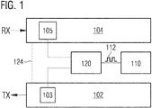
- Fig. 1 illustrates an example of a transceiver circuit for a wireless communication system.
- the transceiver circuit comprises a transmit path 102, which comprises a first mixing circuit 103. Further, the transceiver circuit comprises a receive path 104, which comprises a second mixing circuit 105.
- a local oscillator circuit 110 is configured to generate a local oscillator signal 112 to be used within the mixing circuit 103 and the second mixing circuit 105 to up- or downconvert baseband signals or radio frequency signals.
- the transmit path 102 comprises components or circuitry required to generate a wireless communication signal that can, for example, be provided to an antenna radiator so as to be radiated into the environment.
- transmit paths 102 may comprise a power amplifier (PA) in front of or upstream the antenna radiator to amplify a radio frequency signal generated within the transmit path.
- PA power amplifier
- the receive path 104 contains circuitry or elements required to process signals as received from an antenna's radiator in order to determine information received by, for example, a received radio frequency signal.
- the receive path serves to receive data signals during a normal operation mode of the wireless communication circuit, while the same receive path may serve for calibration purposes in a calibration mode.
- the receive path may be a dedicated receive path which is used for monitoring/calibration only while a further receive path is used to receive data in the normal operation mode.
- a transmit path may optionally further include a modulation circuit in order to convert the information to be submitted to a baseband signal according to the presently used modulation scheme. Further, as subsequent mixing circuitry to up-convert the baseband signal to the radio frequency signal used to radiate the information may be present.
- receive paths 104 may include a down converter and a subsequent demodulation circuit in order to recover the logical information transported by means of the radio frequency communication signal.
- transmit path 102 and receive path 104 as used herein shall not be construed to include all the components technically necessary in order to generate a radio frequency signal or to recover the logical information transmitted by means of the radio frequency signal.
- a transmit path 102 or a receive path 104 as used in the context of the present description may comprise only a subset of those components or elements.
- a delay circuit 120 is configured to delay the local oscillator signal 112 for the mixing circuit 103 or for the second mixing circuit 105 by an adjustable time difference.
- Having the capability of delaying the local oscillator signal 112 used by the first mixing circuit 103 or the second mixing circuit 105 allows to timely align the use of the local oscillator signal within both mixing circuits 103 and 105. Assuring that the local oscillator signals are used within the mixing circuits 103 and 105 timely aligned may result in close to perfect cancellation of phase noise impairments during a loopback calibration of the transceiver circuit.
- a calibration signal generated within the transmit path 102 is deliberately coupled into the receive path 104.
- the receive path measures the received calibration signal generated by the transmit path 102 and determines its quality using an appropriate metric.
- the goal is to use the identical phase (clock cycle and phase) of the local oscillator signal 112 to down convert a particular signal portion of the received calibration signal in the second mixing circuit 105 which was used to up convert the corresponding (identical) signal portion of the calibration signal within the first mixing circuit 103. Achieving this, one may mitigate or eliminate the effects of phase noise of the local oscillator signal 112.
- the local oscillator signal for both the first mixing circuit 103 and the second mixing circuit 105 is generated by local oscillator circuit 110 and distributed to the first mixing circuit 103 and the second mixing circuit 105.
- a time difference to be compensated by means of the delay circuit 120 may originate from various effects within the transceiver circuit, for example from different lengths of the signal lines between the local oscillator circuit 110 and the first mixing circuit 103 or the second mixing circuit 105 as well as from the signal propagation time between the first mixing circuit 103 and the second mixing circuit 105. All causes of time differences can be considered to timely align the use of the local oscillator signal 112 without the necessity of identifying their root cause.
- the delay circuit 120 is configured to delay the local oscillator signal 112 for the first mixing circuit 103 or for the second mixing circuit 105 such that identical phases of the local oscillator signal are used by the mixing circuit 103 and the second mixing circuit 105 simultaneously.
- the resultant time difference of the use of an identical phase of the local oscillator signal 112 at the mixing circuit 103 and at the second mixing circuit 105 may be less than 30% of a nominal cycle time of the local oscillator signal 112 to achieve a decrease of phase noise impairments.
- Further examples may provide a time difference of less than 10% of the nominal cycle time, which may provide a greater decrease of the phase noise impairments or which may provide the decrease of phase noise impairments for higher radio frequencies. For the same reason, some examples may provide a time difference of less than 2% of the nominal cycle time.
- a loopback calibration a loopback path between the transmit path and the receive path of the transceiver is used or closed so that a signal generated within the transmit path is deliberately coupled into the receive path.
- the receive path measures the signal generated by the transmit path and determines its quality using an appropriate metric.
- a loopback calibration is the determination of a pre-distortion model for a power amplifier within the transmit path.
- the nonlinearities and memory effects being inherent to the power amplifier are determined and, based on the so-determined pre-distortion model, the signal to be amplified by means of the power amplifier is processed in anticipation of the power amplifier's imperfections (e.g. within the baseband) so as to receive, as a net effect, a signal which is close to linear amplification and perfect phase preservation over the whole dynamic range of the power amplifier.
- An optional loopback 124 path between the transmit path 102 and the receive path 104 is illustrated in fig. 1 .
- the loopback path 124 may have an arbitrary configuration.
- the loopback path 124 may further comprise an attenuation element so as to appropriately attenuate the transmit path's output signal to avoid exceeding the receive path's dynamic range.
- the model e.g. a pre-distortion model, determined by the loopback calibration can be determined with a greater accuracy. This, in turn, may result in a higher quality of the signal generated by the transmit path 102, if the model determined by the loopback calibration is used during normal operation to pre-distort the signal or to correct for other imperfections of components within the transmit path 102. Consequently, when the time difference between the use of the local oscillator signal 112 within the transmit path 102 and the receive path 104 is decreased according to the examples described herein, a transceiver circuit can be provided which generates a transmit signal that may be compliant also with highly-demanding signal quality requirements.
- While some examples may use a receive path for the loopback calibration which is also used during a normal operation mode to receive signals containing payload, further examples may optionally use a receiver which is implemented for the purpose of performing loopback calibrations only (a loopback-receiver). Some examples using loopback receivers may optionally comprise a loopback path which permanently couples the transmit path 102 and the receive path 104.
- transceiver circuits further optionally comprise a pre-distortion estimation circuit configured to calculate a pre-distortion model for a power amplifier within the transmit path during the loopback calibration.
- a second calibration signal may be transmitted by the transmit path while the loopback path is closed in order to determine the pre-distortion model using a local oscillator signal having a low time delay between its use by the mixing circuit of the transmit path and the second mixing circuit of the receive path.
- the mixing circuit and the second mixing circuit may provide for a loopback calibration having almost no impairments due to the local oscillator signal's phase noise and hence provide a precise pre-distortion model for the power amplifier. This, in turn, may result with a transmit path providing a transmit signal complying with highly-demanding performance requirements.
- Some examples may optionally further comprise a pre-distortion circuit which is configured to modify a transmit signal using the pre-distortion model determined during the loopback calibration.
- the delay circuit may be configured to delay the local oscillator signal for the mixing circuit and for the second mixing circuit such that identical phases of the local oscillator signal are used by the first mixing circuit and by the second mixing circuit with a time difference of less than 10% of a nominal cycle time of the local oscillator signal.
- the delay may be determined with an accuracy of 10% of the cycle time.
- Fig. 2 illustrates an example of a transceiver circuit having a transmit path 202 and a receive path 204.
- the exemplary transmit and receive paths use I/Q modulation. Further examples may optionally also use direct synthesis or Polar Transmitters.
- the transceiver circuit further comprises a local oscillator circuit 219 configured to generate a local oscillator signal for a first mixing circuit 216 and for a second mixing circuit 232.
- the transmit path 202 serves to create a radio frequency signal from a baseband signal, the baseband signal comprising the information to be transmitted via the radio frequency signal.
- a baseband modulator 210 within the transmit path 202 creates both an I-component and a Q-component of the baseband signal.
- a first digital-to-analog converter 212a and a second digital-to-analog converter 212b serve to create analog representations of the I-component and Q-component, each digital-to-analog converter followed by low path filters 214a and 214b to clear the spectrum, for example deleting alias components.
- a mixer circuit 216 is used to up-convert the I-component and the Q-component and to sum up both up-converted components to provide the radio frequency signal.
- the so-generated radio frequency signal is amplified by means of a power amplifier 218.
- An output of the power amplifier 218 is connectable to a radiator of an antenna system in order to radiate the amplified radio frequency signal into an environment.
- the connection between the power amplifier 218 and the radiator can optionally be opened and closed, for example by means of a switch.
- the receive path 204 comprises a low-noise amplifier 230 which is connectable to a receive antenna radiator.
- the received radio frequency signal is down-converted by means of the second mixing circuit 232 which is also separating the I-component and the Q-component of the down-converted baseband signal from one another.
- Low path filters 234a and 234b serve to clean the spectrum before the analog representation of the I-component and the Q-component is digitized by means of analog-to-digital converters 236a and 236b.
- a delay circuit 220 is configured to delay the local oscillator signal for the mixing circuit 216 or for the second mixing circuit 232 by an adjustable time difference.
- the delay circuit 220 optionally is configured to delay the local oscillator signal for the first mixing circuit 216 or for the second mixing circuit 232 such that identical phases of the local oscillator signal are used by the first mixing circuit 216 and by the second mixing circuit 232 at a time.
- the time difference between identical phases of the local oscillator is less than 10%, 20% or 30% of a nominal cycle time of the local oscillator signal.
- the delay circuit 220 comprises a first delay element 222a for the second mixing circuit 232 and a second delay element 222b for the first mixing circuit 216.
- At least the delay element for the mixing circuit with the antecedent phase is used to timely align the local oscillator signals used within the first mixing circuit 216 and the second mixing circuit 232. Further examples may optionally always use both delay elements 222a and 222b. Optionally, only a single delay element may be present while the output of the delay element is dynamically routed to the mixing circuit using the local oscillator with the antecedent phase.
- the pre-distortion estimation circuit 240 serves to calculate a pre-distortion model for the power amplifier 218 during a loopback calibration.
- the pre-distortion model is calculated while a loopback path 250 between the transmit path 202 and the receive path 204 is closed so that a second calibration signal generated within the transmit path 202 and amplified by means of power amplifier 218 is coupled (looped back) into the receive path 204.
- two loopback paths 250 and 260 are used.
- the first loopback path 250 comprises a first switch 252, a second switch 254 and a variable attenuation element 256 between the first switch 252 and the second switch 254.
- loopback 250 path between the transmit path 202 and the receive path 204 can be closed in order to enable loopback calibration.
- switches 262 and 264 of the second loopback path 260 serve for the same purpose.
- the transmitter transmits the second calibration signal via the transmit path 202 into the receive path 204.
- the receive path 204 receives the second calibration signal and the pre-distortion estimation circuit 240 calculates a pre-distortion model for the power amplifier 218 using the transmitted second calibration signal and the corresponding received second calibration signal.
- Loopback path 250 is coupled to the transmit path 202 downstream power amplifier 218, while loopback path 260 is coupled to the transmit path 202 upstream power amplifier 218.
- Performing loopback calibration with timely aligned local oscillator signals used within the mixing circuit 216 and the second mixing circuit 232 may result with a predistortion model and a transmitter providing a signal compliant with high quality requirements, e.g. with respect to an error vector magnitude (EVM) or with respect to a spectral mask.
- EVM error vector magnitude
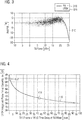
- Figs. 3 and 5 illustrate, on the x-axis, the transmit power of a signal generated within the transmit path 202 using the power amplifier 218.
- the y-axis illustrates AM/PM distortion, i.e. a deviation of the desired phase preservation characteristics of the power amplifier from the power amplifier's real behavior.
- power amplifiers exhibit AM/PM as well as AM/AM distortion.
- Figs. 3 and 5 illustrate the determination of an AM/PM part of a predistortion model to be considered to arrive at a transmit path that does not alter the phase of the signal when it comes to high transmit powers.
- the solid line 310 of Fig. 3 illustrates the phase distortion introduced by means of the power amplifier 218 depending on the signal strength.
- the point cloud illustrates the results obtained from AM/PM distortion measurement, determined by means of a loopback calibration for multiple measurements. As apparent from Fig. 3 , caused by the phase noise of the local oscillator signal, the individual measurements are randomly distributed around the real value and the width of the distribution is significant.
- the distribution is caused by the fact that, when the local oscillator signals at first mixing circuit 216 and at second mixing circuit 232 are not time aligned, the transmitted second calibration signal within the transmitter is up-converted using a local oscillator signal having a different instantaneous phase than the received second calibration signal, which is down-converted using a local oscillator signal having a different instantaneous phase. If the rising and falling edges of the local oscillator signal would be perfectly equally spaced, this may not cause a problem. However, real local oscillator signals exhibit phase noise, i.e. the rising and falling edges of the oscillator signals deviate randomly from their desired nominal positions.
- TX(t) denotes the second calibration signal generated within the transmit path 204 and used for the loopback calibration.
- This signal is up-converted by means of the first mixing circuit 216, providing the term cos( ⁇ t + PN(t)), with PN ( t ) being the deviation at time t caused by phase noise.
- the down-conversion in the receive path 204 provides for the term cos( ⁇ ( t - ⁇ ) + PN ( t - ⁇ )), in which the delay between the use of the local oscillator signal in the first mixing circuit 216 and in the second mixing circuit 232 is given by means of ⁇ .
- the applied delay D (adjustable time difference) is chosen such that D is approximately equal to ⁇ so that the impairments due to phase noise would be canceled:
- LPBK t TX t ⁇ cos PN t ⁇ D ⁇ PN t ⁇ ⁇ ⁇ TX t .
- some examples may delay the local oscillator signal for the first mixing circuit or for the second mixing circuit such that identical phases of the local oscillator signal are used by the mixing circuit and by the second mixing circuit for identical signal portions to be up- or down converted.
- Fig. 5 illustrates the result of loopback calibration after the local oscillator signal within the first mixing circuit 216 and within the second mixing circuit 232 have been timely aligned with a resolution of 30 psec. As illustrated in Fig. 5 , if such a time alignment is achieved, the AM/PM distortion determined during loopback calibration corresponds to the real AM/PM distortion of the power amplifier 218 within the measurement limits.
- the phase noise-induced distortion as illustrated in Fig. 3 would result with an EVM (at 10 dB below OP 5dB) even after application of a pre-distortion model for the power amplifier's nonlinearity of -38dB.
- EVM at 10 dB below OP 5dB
- the loopback calibration is performed with the local oscillator signals being timely aligned, using the pre-distortion model determined during the loopback calibration would drop to -45dB. That is, the transmit path's EVM due to linearity only would jump from -45dB to -38dB if the time alignment was not used, which may be insufficient for many Wi-Fi MCSs (Modulation and Coding Schemes).
- a target EVM may be -43dB.
- a loopback calibration the determination of a pre-distortion model
- MCS modulation coding schemes
- the cancelation of phase noise is a function of the delay time or of the resolution achieved for the alignment of the local oscillator signals.
- Fig. 4 presents the integrated phase noise cancelation as a function of the transmitter (TX) local oscillator signal vs. the receiver (RX) local oscillator signal (LO) time delay at the second mixing circuit 232 of the receive path 204.
- the x-axis of Fig. 4 illustrates the remaining time delay between the two local oscillator signals and the y-axis illustrates the associated integrated phase noise cancellation.
- the delay alignment resolution may be chosen to match a desired level of phase noise cancelation. For example, as illustrated by means of marker 412 in Fig. 4 , for a cancelation of 65 dB, a resolution of 2psec would be required, while for a cancelation of 40 dB (marker 414) a resolution of the 30psec would be sufficient.
- a loopback calibration used to eventually meet certain signal quality requirements for today's and future transceiver circuits may itself be subject to various imperfections, which potentially affect the loopback calibration mechanisms and degrade performance.
- One of those loopback impairments may be local oscillator (LO) phase noise (PN).
- LO local oscillator
- PN phase noise
- the local oscillator phase noise may introduce loopback AM/PM distortion, and thus degrade loopback calibration performance (e.g. resulting in a degraded pre-distortion model).
- MPAPD Memory Power Amplifier Pre-Distortion
- High bandwidths experience high integrated phase noise since the further the phase noise impairments increase, the greater the bandwidth is and the further the observed channel is spaced from the center of frequency of the carrier.
- the examples described herein choose a novel approach of optimizing phase noise cancelation over the overall loopback path by calibrating the time delay between the use of the local oscillator signal within the transmit path (TXLO) and within the receive path (RXLO) within the receive path's mixer circuit.
- TXLO transmit path
- RXLO receive path
- the loopback phase noise (deterioration of the loopback calibration due to the phase noise) may be extremely low and introduce practically close to zero distortion (for example, phase noise-induced loopback AM/PM distortion for Power Amplifier Pre-Distortion, PAPD).
- PAPD Power Amplifier Pre-Distortion
- examples described herein may provide even better cancelation at lower design or implementation complexity.
- Loopback calibration phase noise cancelation degrades over frequency offset (from the frequency of the local oscillator signal).
- this effect may be considerable, since the determination of the pre-distortion model may require high bandwidth (up to 470 MHz for 160 MHz signals) and, therefore, would not enjoy high cancellation across its full observation bandwidths if based on conventional approaches.
- the resultant increased loopback integrated phase noise would require even more stringent performance requirements for the hardware (synthesized LO, delay) which would be very difficult and almost impossible to meet by design and, if so, be extremely expensive during the conceptual phase.
- the examples described herein do not try to minimize the phase noise impairments of the loopback calibration by design but rather cancel the phase noise impairment by adjusting (time delaying) the transmit/receive loopback paths to exhibit the same (up to some degree) time degree of TXLO and RXLO at the RX mixer.
- This results in low integrated phase noise within the loopback calibration, even at high frequency offsets and over ultra-wide integration bandwidths, which is a critical use case, in particular because of MPAPD calibration, i.e. the necessity to pre-distort signals for power amplifiers in order to enable transmitters being compliant with even highly demanding performance requirements.
- an optional leakage estimation circuit 206 serves to perform both calculating a leakage model between the transmit path 202 and the receive path 204 and using the leakage model to compensate leakage between the transmit path 202 and the receive path 204 during the loopback calibration of the transceiver of Fig. 2 .
- the leakage model comprises the same contributions for the power amplifier 210 within the transmit path 202 as the model used for the loopback calibration, good pre-distortion models may be determined.
- the power amplifier 218 and the low-noise amplifier 230 may be disconnected from their antennas by switches or the like. With the given setup, the contribution of leakage between the transmit path 202 and the receive path 204 can optionally be considered during the loopback calibration.
- Fig. 6 illustrates a flowchart of an example of a method for increasing an accuracy of a transceiver loopback calibration.
- the method comprises determining a time difference 602 between the use of the local oscillator signal by a second mixing circuit within a receive path of the transceiver and the use of the local oscillator signal by a first mixing circuit within a transmit path of the transceiver.
- the method further comprises delaying the local oscillator signal 604 to reduce the time difference.
- the method comprises performing a loopback calibration 606 of the transceiver.
- the loopback calibration comprises closing a loopback path 612 between the transmit path and the receive path and transmitting a further calibration signal 614 via the transmit path.
- the method comprises receiving the further received calibration signal via the receive path 616.
- the method comprises calculating a pre-distortion model 618 for the transmit path using the further received calibration signal and the further calibration signal.
- the pre-distortion model may serve to provide a transmitter fulfilling desired net requirements, e.g. with respect to the spectral mask or to the EVM.
- Fig. 7 illustrates flowcharts for three optional methods to determine the time difference 602.
- determining the time difference may comprise closing the loopback path 712 between the transmit path and the receive path of the transceiver. With closed loopback path, integrated receive phase noise values within the receive path are determined in step 714 for different delays applied to one of the local oscillator signals. Further, the method comprises measuring an integrated transmitter phase noise value 716, e.g. by performing a simple direct measurement of the transmit signal.
- the time difference is determined in step 718.
- the dependency on the integrated phase noise cancelation on the time delay as illustrated in Fig. 4 may be used to determine the required time delay.
- the measured integrated transmitter phase noise value and the various receive phase noise values can be used to determine the phase noise cancelation as a function of the delay time and the delay time associated to the desired phase noise cancelation can be selected.
- the first optional example measures the loopback integrated phase noise vs. the LO to TX/RX path delay.
- the integrated phase noise cancelation is calculated based on the synthesizer integrated phase noise measurement (performed, e.g. by a simple direct TX measurement) and, from this data, the delay can be extracted.
- determining the time difference may further comprise measuring a phase characteristic within the receive path as a function of an output path of the transmit path, as for example illustrated in Fig. 3 . That is, for example, the loopback AM/PM distortion may be measured vs. the LO to TX/RX path delay. From this data, the integrated phase noise is a function of the time difference that can be calculated from that data and used as one of the inputs of the previously discussed methods.
- the second optional method to determine the time difference comprises closing the loopback path 722. Further, the method comprises transmitting a second calibration signal 724 via the transmit path and detecting the second calibration signal 726 within the receive path. Further, the method comprises determining a second time difference 728 between the detected and the transmitted second calibration signal. Further, the method comprises correcting the second time difference 730 by signal propagation times of the transmit path and the receive path to determine the time difference.
- a known signal pattern having beneficial signal properties may, for example, be injected to the digital-to-analog converters 212a and 212b of the transmit path 202 of Fig. 2 .
- these signals may be generated or provided by means of baseband modulator 210.
- the known signal pattern may be detected at or after the ADCs 236a and 236b, for example by performing a correlation between the signal injected into the DACs 212a and 212b and the signals delivered by the ADCs 236a and 236b.
- the so-determined time difference can, for example, be corrected for additional delays caused by the propagation of the data and RF signals within the transmit and receive paths (which are not related to any local oscillator signal delays), since both of these can be measured independently, for example using an open-loop test equipment.
- the third optional method for the determination of the time difference of Fig. 7 comprises closing the loopback path 732 and transmitting a calibration signal 734 via the transmit path. Further, the method comprises receiving a receive calibration signal 736 via the receive path. Further, the method comprises calculating a signal propagation model 738 between the transmit path and the receive path using the received calibration signal and the calibration signal. Further, the method comprises determining the time difference 740 using the signal propagation model.
- a signal propagation model between the transmit path and the receive path may be established for the loopback calibration or separately therefrom, in which the time difference between the use of the local oscillator signals in the first and second mixing circuits is one of the parameters to be optimized. Once the signal model has been determined, for example similar to the algorithm used for the determination of the pre-distortion model, the time difference may be directly extracted from the signal propagation model.
- Fig. 7 briefly illustrates three different methods to determine the time difference
- the time difference may optionally be determined using arbitrary alternative approaches.
- an indirect delay determination or characterization may be based on an evaluation of the result of the transmitter's performance after the loopback calibration (after the determination of the pre-distortion model).
- performance criteria of the loopback calibration EVM, spectral mask, band edge emissions
- MPAPD loopback integrated phase noise on the performance of the loopback calibration algorithm
- An adaptive closed loop delay selection/adjustment algorithm may also be established, based on the transmitter's EVM and PSD values (mask and edge emissions).
- the delaying of the local oscillator signal may be implemented in arbitrary ways.
- a fine delay may be achieved by implementing a combination of two mechanisms.
- a coarse delay may be applied, which may be implemented by a digital circuit capable of adding delays of quarter/half/full LO clock cycles. These circuits are sometimes called “swal-lowers", being capable to figuratively swallow half LO clock periods and thus, effectively, introduce time delay.
- additional delays with finer resolution may be added.
- the coarse step may be combined with a tunable delay line, which may, for example, be varactor-based.
- An alternative implementation for the fine step would be selectable fixed delay lines, e.g. several binary weighted delay lines with series selection switches. The number of delay lines can, of course, be reduced to a number great enough to fulfill the time resolution requirements of the particular implementation.
- Using the examples described herein may even provide a transmit signal reaching similar performance goals (nonlinearity, transmit EVM, transmit IQ imbalance, IQ skew and any other performance criterion which is not masked by phase noise) when the local oscillator within the transmission circuit is injection locked to an external oscillator with high integrated phase noise. This may be achieved since an internal loopback calibration is desensitized to local oscillator's phase noise according to the examples described herein. Injection locking may occur if an internal local oscillator is electromagnetically coupled to an external oscillator, which may exhibit bad phase noise characteristics. If a transceiver circuit under observation is operated within an injection locking setup, it may nonetheless provide for a transmit signal fulfilling high quality requirements.
- Injection locking may be achieved by, for example, using a synthetically generated digital waveform together with a vector signal generator.
- a signal generator having a frequency modulation capability and configuring it to output a high phase noise signal (intended as wideband FM noise).
- a further possibility was to use a basic signal generator set to output a very low level CW signal and amplifying that signal with power amplifiers. The amplifiers would then introduce a very high level wide band thermal noise, determined and characterized by the cascaded gain and NF.
- a further simple implementation to achieve injection locking would be to connect a basic signal generator output to an RF splitter/combiner together with a noise diode with high excess noise ratio (ENR).
- ELR excess noise ratio
- Fig. 8 schematically illustrates an example of a mobile telecommunications device 800 comprising a wireless communication circuit 810, as here illustrated and according to one of the examples described herein.
- the wireless communication circuit within the mobile telecommunications device 810 may be coupled to one or to both of the antenna radiators 820a and 820b of the mobile telecommunications device 800, while further examples may also use an arbitrary higher number of radiators.
- the mobile or wireless communication system may correspond to, for example, a Long-Term Evolution (LTE), an LTE-Advanced (LTE-A), High Speed Packet Access (HSPA), a Universal Mobile Telecommunication System (UMTS) or a UMTS Terrestrial Radio Access Network (UTRAN), an evolved-UTRAN (e-UTRAN), a Global System for Mobile communication (GSM) or Enhanced Data rates for GSM Evolution (EDGE) network, a GSM/EDGE Radio Access Network (GERAN), or mobile communication networks with different standards, for example, a Worldwide Inter-operability for Microwave Access (WIMAX) network IEEE 802.16 or Wireless Local Area Network (WLAN) IEEE 802.11, generally an Orthogonal Frequency Division Multiple Access (OFDMA) network, a Time Division Multiple Access (TDMA) network, a Code Division Multiple Access (CDMA) network, a
- OFDMA Orthogonal Frequency Division Multiple Access
- TDMA Time Division Multiple Access
- CDMA Code Division Multiple Access
- Example 1 is a method for increasing an accuracy of a transceiver loopback calibration, comprising determining a time difference between the use of a local oscillator signal by a second mixing circuit within a receive path of the transceiver and the use of the local oscillator signal by a first mixing circuit within a transmit path of the transceiver; delaying the local oscillator signal for the first mixing circuit or for the second mixing circuit to reduce the time difference; and performing a loopback calibration of the transceiver at the reduced time difference.
- determining the time difference comprises closing a loopback path between a transmit path and a receive path of the transceiver; measuring integrated receive phase noise values within the receive path for different delays of the local oscillator signal; measuring an integrated transmitter phase noise value within the transmit path; and determining the time difference using the integrated receive phase noise values and the integrated transmitter phase noise value.
- determining the time difference comprises measuring a phase characteristic within the receive path as a function of an output power of the transmit path.
- determining the time difference comprises closing a loopback path between the transmit path and the receive path of the transceiver; transmitting a calibration signal via the transmit path; detecting the calibration signal within the receive path; determining a second time difference between the detected and the transmitted calibration signal; and correcting the second time difference by signal propagation times of the transmit path and the receive path to determine the time difference.
- determining the time difference comprises closing a loopback path between the transmit path and the receive path of the transceiver; transmitting a calibration signal via the transmit path; receiving the calibration signal via the receive path; and calculating a signal propagation model between the transmit path and the receive path using the received and the transmitted calibration signal; and determining the time difference using the signal propagation model.
- performing the loopback calibration comprises closing a loopback path between the transmit path and the receive path of the transceiver; transmitting a second calibration signal via the transmit path; receiving the second calibration signal via the receive path; and calculating a predistortion model for the transmit path using the received and the transmitted second calibration signal.
- Example 8 is a transceiver circuit for a wireless communication system, comprising a transmit path comprising a first mixing circuit; a receive path comprising a second mixing circuit; a local oscillator circuit configured to generate a local oscillator signal for the first mixing circuit and for the second mixing circuit; and a delay circuit configured to delay the local oscillator signal for the first circuit or for the second mixing circuit by an adjustable time difference.
- the transceiver circuit of example 8 further comprises at least one loopback path between the transmit path and the receive path.
- the loopback path comprises at least one switch and at least one attenuation element.
- the attenuation element is adjustable.
- the loopback path comprises a first switch between the transmit path and the attenuation element; and a second switch between the attenuation element and the receive path.
- the transceiver circuit of example 12 further comprises a predistortion estimation circuit configured to calculate a predistortion model for a power amplifier within the transmit path using a second calibration signal transmitted via the transmit path when the loopback path is closed.
- the transceiver circuit of examples 13 or 14 further comprises a predistortion circuit in the transmit path, the predistortion circuit being configured to modify a transmit signal using the predistortion model.
- the delay circuit is configured to delay the local oscillator signal for the first mixing circuit or for the second mixing circuit such that identical phases of the local oscillator signal are used by the first mixing circuit and the second mixing circuit with a time difference of less than 30% of a nominal cycle time of the local oscillator signal.
- the time difference is less than 10% or less than 3% of a nominal cycle time of the local oscillator signal.
- the transceiver circuit of example 9 further comprises a further loopback path between the transmit path and the receive path which is coupled to the transmit path upstream of a power amplifier of the transmit path, wherein the loopback path is coupled to the transmit path downstream the power amplifier.
- Example 19 is a transceiver for a wireless communication signal, the transceiver comprising the transceiver circuit of any of examples 8 to 18.
- the transceiver of example 19 further comprises a switching element between the transmit path and an antenna port for coupling the transmitter to a radiator.
- Example 21 is a mobile telecommunications device, comprising a transceiver circuit according to any of examples 8 to 18.
- the mobile telecommunications device of example 21 further comprises a radiator configured to couple to the transmit path and to the receive path of the transceiver circuit.
- the mobile telecommunications device of example 21 further comprises a first radiator configured to couple to the transmit path; and a second radiator configured to couple to the receive path.
- Example 24 is means for increasing an accuracy of a transceiver loopback calibration, comprising means for determining a time difference between the use of a local oscillator signal by a second mixing circuit within a receive path of the transceiver and the use of the local oscillator signal by a first mixing circuit within a transmit path of the transceiver; means for delaying the local oscillator signal for the first mixing circuit or for the second mixing circuit to reduce the time difference; and means for performing a loopback calibration of the transceiver at the reduced time difference.
- the means for performing the loopback calibration comprise means for closing a loopback path between the transmit path and the receive path of the transceiver means for transmitting a second calibration signal via the transmit path; means for receiving the second calibration signal via the receive path; and means for calculating a predistortion model for the transmit path using the received second calibration signal and the transmitted second calibration signal.
- Examples may further be a computer program having a program code for performing one or more of the above methods, when the computer program is executed on a computer or processor. Steps, operations or processes of various above-described methods may be performed by programmed computers or processors. Examples may also cover program storage devices such as digital data storage media, which are machine, processor or computer readable and encode machine-executable, processor-executable or computer-executable programs of instructions. The instructions perform or cause performing some or all of the acts of the above-described methods.
- the program storage devices may comprise or be, for instance, digital memories, magnetic storage media such as magnetic disks and magnetic tapes, hard drives, or optically readable digital data storage media.
- FIG. 1 may also cover computers, processors or control units programmed to perform the acts of the above-described methods or (field) programmable logic arrays ((F)PLAs) or (field) programmable gate arrays ((F)PGAs), programmed to perform the acts of the above-described methods.
- a functional block denoted as "means for " performing a certain function may refer to a circuit that is configured to perform a certain function.
- a "means for s.th.” may be implemented as a "means configured to or suited for s.th.”, such as a device or a circuit configured to or suited for the respective task.
- Functions of various elements shown in the figures may be implemented in the form of dedicated hardware, such as “a signal provider”, “a signal processing unit”, “a processor”, “a controller”, etc. as well as hardware capable of executing software in association with appropriate software.
- a processor the functions may be provided by a single dedicated processor, by a single shared processor, or by a plurality of individual processors, some of which or all of which may be shared.
- processor or “controller” is by far not limited to hardware exclusively capable of executing software, but may include digital signal processor (DSP) hardware, network processor, application specific integrated circuit (ASIC), field programmable gate array (FPGA), read only memory (ROM) for storing software, random access memory (RAM), and nonvolatile storage.
- DSP digital signal processor
- ASIC application specific integrated circuit
- FPGA field programmable gate array
- ROM read only memory
- RAM random access memory
- nonvolatile storage Other hardware, conventional and/or custom, may also be included.
- a block diagram may, for instance, illustrate a high-level circuit diagram implementing the principles of the disclosure.
- a flow chart, a flow diagram, a state transition diagram, a pseudo code, and the like may represent various processes, operations or steps, which may, for instance, be substantially represented in computer readable medium and so executed by a computer or processor, whether or not such computer or processor is explicitly shown.
- Methods disclosed in the specification or in the claims may be implemented by a device having means for performing each of the respective acts of these methods.
- each claim may stand on its own as a separate example. While each claim may stand on its own as a separate example, it is to be noted that - although a dependent claim may refer in the claims to a specific combination with one or more other claims - other example examples may also include a combination of the dependent claim with the subject matter of each other dependent or independent claim. Such combinations are explicitly proposed herein unless it is stated that a specific combination is not intended. Furthermore, it is intended to include also features of a claim to any other independent claim even if this claim is not directly made dependent to the independent claim.
Landscapes
- Physics & Mathematics (AREA)
- Electromagnetism (AREA)
- Engineering & Computer Science (AREA)
- Computer Networks & Wireless Communication (AREA)
- Signal Processing (AREA)
- Transmitters (AREA)
- Transceivers (AREA)
Priority Applications (2)
| Application Number | Priority Date | Filing Date | Title |
|---|---|---|---|
| EP16189900.0A EP3300267B1 (fr) | 2016-09-21 | 2016-09-21 | Procédé d'amélioration de la précision d'étalonnage de rebouclage d'un émetteur-récepteur et de circuit d'émission-réception |
| PCT/US2017/044783 WO2018057122A1 (fr) | 2016-09-21 | 2017-08-01 | Procédé d'augmentation de la précision d'un circuit d'étalonnage et d'émetteur-récepteur de bouclage d'émetteur-récepteur |
Applications Claiming Priority (1)
| Application Number | Priority Date | Filing Date | Title |
|---|---|---|---|
| EP16189900.0A EP3300267B1 (fr) | 2016-09-21 | 2016-09-21 | Procédé d'amélioration de la précision d'étalonnage de rebouclage d'un émetteur-récepteur et de circuit d'émission-réception |
Publications (2)
| Publication Number | Publication Date |
|---|---|
| EP3300267A1 true EP3300267A1 (fr) | 2018-03-28 |
| EP3300267B1 EP3300267B1 (fr) | 2021-02-24 |
Family
ID=57017964
Family Applications (1)
| Application Number | Title | Priority Date | Filing Date |
|---|---|---|---|
| EP16189900.0A Not-in-force EP3300267B1 (fr) | 2016-09-21 | 2016-09-21 | Procédé d'amélioration de la précision d'étalonnage de rebouclage d'un émetteur-récepteur et de circuit d'émission-réception |
Country Status (2)
| Country | Link |
|---|---|
| EP (1) | EP3300267B1 (fr) |
| WO (1) | WO2018057122A1 (fr) |
Cited By (2)
| Publication number | Priority date | Publication date | Assignee | Title |
|---|---|---|---|---|
| CN114268382A (zh) * | 2022-02-28 | 2022-04-01 | 四川鸿创电子科技有限公司 | 一种自动校准ad9361板卡的方法、装置、设备及存储介质 |
| US20250088287A1 (en) * | 2023-09-07 | 2025-03-13 | Xilinx, Inc. | Transceiver loopback data path |
Families Citing this family (1)
| Publication number | Priority date | Publication date | Assignee | Title |
|---|---|---|---|---|
| CN119945651B (zh) * | 2025-04-03 | 2025-06-10 | 成都维德青云电子有限公司 | 收发器延迟校准系统及方法 |
Citations (4)
| Publication number | Priority date | Publication date | Assignee | Title |
|---|---|---|---|---|
| WO2013028296A1 (fr) * | 2011-08-24 | 2013-02-28 | Rambus Inc. | Étalonnage d'un réseau rétrodirectif pour une liaison sans fil asymétrique |
| WO2013056398A1 (fr) * | 2011-10-21 | 2013-04-25 | Telefonaktiebolaget L M Ericcson (Publ) | Procédés, dispositif de traitement, programmes informatiques, produits programmes d'ordinateur et appareil formant antenne pour l'étalonnage d'un appareil formant antenne |
| US20150030102A1 (en) * | 2013-07-25 | 2015-01-29 | Analog Devices, Inc. | Wideband quadrature error correction |
| US20160149652A1 (en) * | 2014-11-20 | 2016-05-26 | Mediatek Inc. | SCHEME FOR PERFORMING BEAMFORMING CALIBRATION BY MEASURING JOINT SIGNAL Path MISMATCH |
Family Cites Families (4)
| Publication number | Priority date | Publication date | Assignee | Title |
|---|---|---|---|---|
| US8498591B1 (en) * | 2009-08-21 | 2013-07-30 | Marvell International Ltd. | Digital Predistortion for nonlinear RF power amplifiers |
| US8908575B2 (en) * | 2012-04-16 | 2014-12-09 | Qualcomm Incorporated | Methods and systems for calibrating a frequency-division duplexing transceiver |
| US9787415B2 (en) * | 2013-03-14 | 2017-10-10 | Analog Devices, Inc. | Transmitter LO leakage calibration scheme using loopback circuitry |
| KR101975789B1 (ko) * | 2014-01-03 | 2019-05-09 | 삼성전자주식회사 | I/q 미스매치 보상을 위한 방법 및 그 장치 |
-
2016
- 2016-09-21 EP EP16189900.0A patent/EP3300267B1/fr not_active Not-in-force
-
2017
- 2017-08-01 WO PCT/US2017/044783 patent/WO2018057122A1/fr not_active Ceased
Patent Citations (4)
| Publication number | Priority date | Publication date | Assignee | Title |
|---|---|---|---|---|
| WO2013028296A1 (fr) * | 2011-08-24 | 2013-02-28 | Rambus Inc. | Étalonnage d'un réseau rétrodirectif pour une liaison sans fil asymétrique |
| WO2013056398A1 (fr) * | 2011-10-21 | 2013-04-25 | Telefonaktiebolaget L M Ericcson (Publ) | Procédés, dispositif de traitement, programmes informatiques, produits programmes d'ordinateur et appareil formant antenne pour l'étalonnage d'un appareil formant antenne |
| US20150030102A1 (en) * | 2013-07-25 | 2015-01-29 | Analog Devices, Inc. | Wideband quadrature error correction |
| US20160149652A1 (en) * | 2014-11-20 | 2016-05-26 | Mediatek Inc. | SCHEME FOR PERFORMING BEAMFORMING CALIBRATION BY MEASURING JOINT SIGNAL Path MISMATCH |
Cited By (4)
| Publication number | Priority date | Publication date | Assignee | Title |
|---|---|---|---|---|
| CN114268382A (zh) * | 2022-02-28 | 2022-04-01 | 四川鸿创电子科技有限公司 | 一种自动校准ad9361板卡的方法、装置、设备及存储介质 |
| CN114268382B (zh) * | 2022-02-28 | 2022-05-13 | 四川鸿创电子科技有限公司 | 一种自动校准ad9361板卡的方法、装置、设备及存储介质 |
| US20250088287A1 (en) * | 2023-09-07 | 2025-03-13 | Xilinx, Inc. | Transceiver loopback data path |
| US12592784B2 (en) * | 2023-09-07 | 2026-03-31 | Xilinx, Inc. | Transceiver loopback data path |
Also Published As
| Publication number | Publication date |
|---|---|
| EP3300267B1 (fr) | 2021-02-24 |
| WO2018057122A1 (fr) | 2018-03-29 |
Similar Documents
| Publication | Publication Date | Title |
|---|---|---|
| US10469109B2 (en) | Predistortion for transmitter with array | |
| US8976845B2 (en) | Communication system, network element and method for antenna array calibration | |
| US11005510B2 (en) | Systems and methods for adaptive averaging in frequency domain equalization systems | |
| CN100459441C (zh) | 发射机和发送方法 | |
| US9692366B2 (en) | Envelope tracking path delay fine tuning and calibration | |
| US9450553B2 (en) | Apparatus and a method for amplifying a transmit signal | |
| CN107863988B (zh) | 计算发射路径和接收路径之间泄漏的方法和无线通信电路 | |
| US8542767B2 (en) | Digital predistortion training system | |
| US8705595B2 (en) | Digital output power measurement in radio communication systems | |
| US20120027066A1 (en) | Communication system, apparatus and methods for calibrating an antenna array | |
| US8774738B2 (en) | Closed loop power control for a wireless transmitter | |
| EP3300267B1 (fr) | Procédé d'amélioration de la précision d'étalonnage de rebouclage d'un émetteur-récepteur et de circuit d'émission-réception | |
| EP4000183A1 (fr) | Annulation de pim | |
| Austin et al. | Digital predistortion of power amplifier non-linearities for full-duplex transceivers | |
| US11374661B2 (en) | Generalized virtual PIM measurement for enhanced accuracy | |
| US11456762B2 (en) | Control device and radio communication device | |
| US10164584B2 (en) | Method to mitigate undesired oscillator frequency modulation effects in-side a synthesizer due to interference signals and synthesizer circuit | |
| KR20190092070A (ko) | Rf 신호 전송 장치 및 그의 제어 방법 | |
| US20180269995A1 (en) | Phase Alignment Among Multiple Transmitters | |
| EP3402098B1 (fr) | Émetteur-récepteur pour un système de communication sans fil et procédés permettant d'augmenter la précision d'étalonnage de bouclage de l'émetteur-récepteur | |
| US20200220564A1 (en) | Transceivers for a wireless communication system, mobile device, and method for improving transceiver loopback calibration accuracy | |
| Guan et al. | Linearity study of path imbalances in multi-level LINC transmitter for wideband LTE application | |
| Lozhkin et al. | Hybrid antenna array predistorter for 5G mm band | |
| EP3300257A1 (fr) | Procédé et circuit de détermination d'un réglage d'un circuit d'adaptation d'impédance | |
| Hesami | Modeling and Linearization of MIMO RF Transmitters |
Legal Events
| Date | Code | Title | Description |
|---|---|---|---|
| PUAI | Public reference made under article 153(3) epc to a published international application that has entered the european phase |
Free format text: ORIGINAL CODE: 0009012 |
|
| STAA | Information on the status of an ep patent application or granted ep patent |
Free format text: STATUS: THE APPLICATION HAS BEEN PUBLISHED |
|
| AK | Designated contracting states |
Kind code of ref document: A1 Designated state(s): AL AT BE BG CH CY CZ DE DK EE ES FI FR GB GR HR HU IE IS IT LI LT LU LV MC MK MT NL NO PL PT RO RS SE SI SK SM TR |
|
| AX | Request for extension of the european patent |
Extension state: BA ME |
|
| STAA | Information on the status of an ep patent application or granted ep patent |
Free format text: STATUS: REQUEST FOR EXAMINATION WAS MADE |
|
| 17P | Request for examination filed |
Effective date: 20180928 |
|
| RBV | Designated contracting states (corrected) |
Designated state(s): AL AT BE BG CH CY CZ DE DK EE ES FI FR GB GR HR HU IE IS IT LI LT LU LV MC MK MT NL NO PL PT RO RS SE SI SK SM TR |
|
| GRAP | Despatch of communication of intention to grant a patent |
Free format text: ORIGINAL CODE: EPIDOSNIGR1 |
|
| STAA | Information on the status of an ep patent application or granted ep patent |
Free format text: STATUS: GRANT OF PATENT IS INTENDED |
|
| INTG | Intention to grant announced |
Effective date: 20200911 |
|
| GRAS | Grant fee paid |
Free format text: ORIGINAL CODE: EPIDOSNIGR3 |
|
| GRAA | (expected) grant |
Free format text: ORIGINAL CODE: 0009210 |
|
| STAA | Information on the status of an ep patent application or granted ep patent |
Free format text: STATUS: THE PATENT HAS BEEN GRANTED |
|
| AK | Designated contracting states |
Kind code of ref document: B1 Designated state(s): AL AT BE BG CH CY CZ DE DK EE ES FI FR GB GR HR HU IE IS IT LI LT LU LV MC MK MT NL NO PL PT RO RS SE SI SK SM TR |
|
| REG | Reference to a national code |
Ref country code: CH Ref legal event code: EP |
|
| REG | Reference to a national code |
Ref country code: DE Ref legal event code: R096 Ref document number: 602016053006 Country of ref document: DE |
|
| REG | Reference to a national code |
Ref country code: AT Ref legal event code: REF Ref document number: 1365820 Country of ref document: AT Kind code of ref document: T Effective date: 20210315 |
|
| REG | Reference to a national code |
Ref country code: IE Ref legal event code: FG4D |
|
| REG | Reference to a national code |
Ref country code: LT Ref legal event code: MG9D |
|
| REG | Reference to a national code |
Ref country code: NL Ref legal event code: MP Effective date: 20210224 |
|
| PG25 | Lapsed in a contracting state [announced via postgrant information from national office to epo] |
Ref country code: LT Free format text: LAPSE BECAUSE OF FAILURE TO SUBMIT A TRANSLATION OF THE DESCRIPTION OR TO PAY THE FEE WITHIN THE PRESCRIBED TIME-LIMIT Effective date: 20210224 Ref country code: GR Free format text: LAPSE BECAUSE OF FAILURE TO SUBMIT A TRANSLATION OF THE DESCRIPTION OR TO PAY THE FEE WITHIN THE PRESCRIBED TIME-LIMIT Effective date: 20210525 Ref country code: HR Free format text: LAPSE BECAUSE OF FAILURE TO SUBMIT A TRANSLATION OF THE DESCRIPTION OR TO PAY THE FEE WITHIN THE PRESCRIBED TIME-LIMIT Effective date: 20210224 Ref country code: FI Free format text: LAPSE BECAUSE OF FAILURE TO SUBMIT A TRANSLATION OF THE DESCRIPTION OR TO PAY THE FEE WITHIN THE PRESCRIBED TIME-LIMIT Effective date: 20210224 Ref country code: BG Free format text: LAPSE BECAUSE OF FAILURE TO SUBMIT A TRANSLATION OF THE DESCRIPTION OR TO PAY THE FEE WITHIN THE PRESCRIBED TIME-LIMIT Effective date: 20210524 Ref country code: NO Free format text: LAPSE BECAUSE OF FAILURE TO SUBMIT A TRANSLATION OF THE DESCRIPTION OR TO PAY THE FEE WITHIN THE PRESCRIBED TIME-LIMIT Effective date: 20210524 Ref country code: PT Free format text: LAPSE BECAUSE OF FAILURE TO SUBMIT A TRANSLATION OF THE DESCRIPTION OR TO PAY THE FEE WITHIN THE PRESCRIBED TIME-LIMIT Effective date: 20210624 |
|
| REG | Reference to a national code |
Ref country code: AT Ref legal event code: MK05 Ref document number: 1365820 Country of ref document: AT Kind code of ref document: T Effective date: 20210224 |
|
| PG25 | Lapsed in a contracting state [announced via postgrant information from national office to epo] |
Ref country code: SE Free format text: LAPSE BECAUSE OF FAILURE TO SUBMIT A TRANSLATION OF THE DESCRIPTION OR TO PAY THE FEE WITHIN THE PRESCRIBED TIME-LIMIT Effective date: 20210224 Ref country code: RS Free format text: LAPSE BECAUSE OF FAILURE TO SUBMIT A TRANSLATION OF THE DESCRIPTION OR TO PAY THE FEE WITHIN THE PRESCRIBED TIME-LIMIT Effective date: 20210224 Ref country code: LV Free format text: LAPSE BECAUSE OF FAILURE TO SUBMIT A TRANSLATION OF THE DESCRIPTION OR TO PAY THE FEE WITHIN THE PRESCRIBED TIME-LIMIT Effective date: 20210224 Ref country code: NL Free format text: LAPSE BECAUSE OF FAILURE TO SUBMIT A TRANSLATION OF THE DESCRIPTION OR TO PAY THE FEE WITHIN THE PRESCRIBED TIME-LIMIT Effective date: 20210224 Ref country code: PL Free format text: LAPSE BECAUSE OF FAILURE TO SUBMIT A TRANSLATION OF THE DESCRIPTION OR TO PAY THE FEE WITHIN THE PRESCRIBED TIME-LIMIT Effective date: 20210224 |
|
| PG25 | Lapsed in a contracting state [announced via postgrant information from national office to epo] |
Ref country code: IS Free format text: LAPSE BECAUSE OF FAILURE TO SUBMIT A TRANSLATION OF THE DESCRIPTION OR TO PAY THE FEE WITHIN THE PRESCRIBED TIME-LIMIT Effective date: 20210624 |
|
| PG25 | Lapsed in a contracting state [announced via postgrant information from national office to epo] |
Ref country code: CZ Free format text: LAPSE BECAUSE OF FAILURE TO SUBMIT A TRANSLATION OF THE DESCRIPTION OR TO PAY THE FEE WITHIN THE PRESCRIBED TIME-LIMIT Effective date: 20210224 Ref country code: EE Free format text: LAPSE BECAUSE OF FAILURE TO SUBMIT A TRANSLATION OF THE DESCRIPTION OR TO PAY THE FEE WITHIN THE PRESCRIBED TIME-LIMIT Effective date: 20210224 Ref country code: AT Free format text: LAPSE BECAUSE OF FAILURE TO SUBMIT A TRANSLATION OF THE DESCRIPTION OR TO PAY THE FEE WITHIN THE PRESCRIBED TIME-LIMIT Effective date: 20210224 Ref country code: SM Free format text: LAPSE BECAUSE OF FAILURE TO SUBMIT A TRANSLATION OF THE DESCRIPTION OR TO PAY THE FEE WITHIN THE PRESCRIBED TIME-LIMIT Effective date: 20210224 |
|
| REG | Reference to a national code |
Ref country code: DE Ref legal event code: R097 Ref document number: 602016053006 Country of ref document: DE |
|
| PG25 | Lapsed in a contracting state [announced via postgrant information from national office to epo] |
Ref country code: DK Free format text: LAPSE BECAUSE OF FAILURE TO SUBMIT A TRANSLATION OF THE DESCRIPTION OR TO PAY THE FEE WITHIN THE PRESCRIBED TIME-LIMIT Effective date: 20210224 Ref country code: SK Free format text: LAPSE BECAUSE OF FAILURE TO SUBMIT A TRANSLATION OF THE DESCRIPTION OR TO PAY THE FEE WITHIN THE PRESCRIBED TIME-LIMIT Effective date: 20210224 Ref country code: RO Free format text: LAPSE BECAUSE OF FAILURE TO SUBMIT A TRANSLATION OF THE DESCRIPTION OR TO PAY THE FEE WITHIN THE PRESCRIBED TIME-LIMIT Effective date: 20210224 |
|
| PLBE | No opposition filed within time limit |
Free format text: ORIGINAL CODE: 0009261 |
|
| STAA | Information on the status of an ep patent application or granted ep patent |
Free format text: STATUS: NO OPPOSITION FILED WITHIN TIME LIMIT |
|
| PG25 | Lapsed in a contracting state [announced via postgrant information from national office to epo] |
Ref country code: ES Free format text: LAPSE BECAUSE OF FAILURE TO SUBMIT A TRANSLATION OF THE DESCRIPTION OR TO PAY THE FEE WITHIN THE PRESCRIBED TIME-LIMIT Effective date: 20210224 Ref country code: AL Free format text: LAPSE BECAUSE OF FAILURE TO SUBMIT A TRANSLATION OF THE DESCRIPTION OR TO PAY THE FEE WITHIN THE PRESCRIBED TIME-LIMIT Effective date: 20210224 |
|
| 26N | No opposition filed |
Effective date: 20211125 |
|
| PG25 | Lapsed in a contracting state [announced via postgrant information from national office to epo] |
Ref country code: SI Free format text: LAPSE BECAUSE OF FAILURE TO SUBMIT A TRANSLATION OF THE DESCRIPTION OR TO PAY THE FEE WITHIN THE PRESCRIBED TIME-LIMIT Effective date: 20210224 |
|
| REG | Reference to a national code |
Ref country code: DE Ref legal event code: R119 Ref document number: 602016053006 Country of ref document: DE |
|
| PG25 | Lapsed in a contracting state [announced via postgrant information from national office to epo] |
Ref country code: IT Free format text: LAPSE BECAUSE OF FAILURE TO SUBMIT A TRANSLATION OF THE DESCRIPTION OR TO PAY THE FEE WITHIN THE PRESCRIBED TIME-LIMIT Effective date: 20210224 |
|
| REG | Reference to a national code |
Ref country code: CH Ref legal event code: PL |
|
| REG | Reference to a national code |
Ref country code: BE Ref legal event code: MM Effective date: 20210930 |
|
| GBPC | Gb: european patent ceased through non-payment of renewal fee |
Effective date: 20210921 |
|
| PG25 | Lapsed in a contracting state [announced via postgrant information from national office to epo] |
Ref country code: IS Free format text: LAPSE BECAUSE OF FAILURE TO SUBMIT A TRANSLATION OF THE DESCRIPTION OR TO PAY THE FEE WITHIN THE PRESCRIBED TIME-LIMIT Effective date: 20210624 Ref country code: MC Free format text: LAPSE BECAUSE OF FAILURE TO SUBMIT A TRANSLATION OF THE DESCRIPTION OR TO PAY THE FEE WITHIN THE PRESCRIBED TIME-LIMIT Effective date: 20210224 |
|
| PG25 | Lapsed in a contracting state [announced via postgrant information from national office to epo] |
Ref country code: LU Free format text: LAPSE BECAUSE OF NON-PAYMENT OF DUE FEES Effective date: 20210921 Ref country code: IE Free format text: LAPSE BECAUSE OF NON-PAYMENT OF DUE FEES Effective date: 20210921 Ref country code: GB Free format text: LAPSE BECAUSE OF NON-PAYMENT OF DUE FEES Effective date: 20210921 Ref country code: FR Free format text: LAPSE BECAUSE OF NON-PAYMENT OF DUE FEES Effective date: 20210930 Ref country code: DE Free format text: LAPSE BECAUSE OF NON-PAYMENT OF DUE FEES Effective date: 20220401 Ref country code: BE Free format text: LAPSE BECAUSE OF NON-PAYMENT OF DUE FEES Effective date: 20210930 |
|
| PG25 | Lapsed in a contracting state [announced via postgrant information from national office to epo] |
Ref country code: LI Free format text: LAPSE BECAUSE OF NON-PAYMENT OF DUE FEES Effective date: 20210930 Ref country code: CH Free format text: LAPSE BECAUSE OF NON-PAYMENT OF DUE FEES Effective date: 20210930 |
|
| PG25 | Lapsed in a contracting state [announced via postgrant information from national office to epo] |
Ref country code: HU Free format text: LAPSE BECAUSE OF FAILURE TO SUBMIT A TRANSLATION OF THE DESCRIPTION OR TO PAY THE FEE WITHIN THE PRESCRIBED TIME-LIMIT; INVALID AB INITIO Effective date: 20160921 |
|
| PG25 | Lapsed in a contracting state [announced via postgrant information from national office to epo] |
Ref country code: CY Free format text: LAPSE BECAUSE OF FAILURE TO SUBMIT A TRANSLATION OF THE DESCRIPTION OR TO PAY THE FEE WITHIN THE PRESCRIBED TIME-LIMIT Effective date: 20210224 |
|
| PG25 | Lapsed in a contracting state [announced via postgrant information from national office to epo] |
Ref country code: MK Free format text: LAPSE BECAUSE OF FAILURE TO SUBMIT A TRANSLATION OF THE DESCRIPTION OR TO PAY THE FEE WITHIN THE PRESCRIBED TIME-LIMIT Effective date: 20210224 |
|
| PG25 | Lapsed in a contracting state [announced via postgrant information from national office to epo] |
Ref country code: TR Free format text: LAPSE BECAUSE OF FAILURE TO SUBMIT A TRANSLATION OF THE DESCRIPTION OR TO PAY THE FEE WITHIN THE PRESCRIBED TIME-LIMIT Effective date: 20210224 |
|
| PG25 | Lapsed in a contracting state [announced via postgrant information from national office to epo] |
Ref country code: MT Free format text: LAPSE BECAUSE OF FAILURE TO SUBMIT A TRANSLATION OF THE DESCRIPTION OR TO PAY THE FEE WITHIN THE PRESCRIBED TIME-LIMIT Effective date: 20210224 |