EP3300472A2 - Composant électrique - Google Patents
Composant électrique Download PDFInfo
- Publication number
- EP3300472A2 EP3300472A2 EP17191571.3A EP17191571A EP3300472A2 EP 3300472 A2 EP3300472 A2 EP 3300472A2 EP 17191571 A EP17191571 A EP 17191571A EP 3300472 A2 EP3300472 A2 EP 3300472A2
- Authority
- EP
- European Patent Office
- Prior art keywords
- component
- projection
- shield
- component according
- switching node
- Prior art date
- Legal status (The legal status is an assumption and is not a legal conclusion. Google has not performed a legal analysis and makes no representation as to the accuracy of the status listed.)
- Granted
Links
Images


Classifications
-
- H—ELECTRICITY
- H05—ELECTRIC TECHNIQUES NOT OTHERWISE PROVIDED FOR
- H05K—PRINTED CIRCUITS; CASINGS OR CONSTRUCTIONAL DETAILS OF ELECTRIC APPARATUS; MANUFACTURE OF ASSEMBLAGES OF ELECTRICAL COMPONENTS
- H05K9/00—Screening of apparatus or components against electric or magnetic fields
- H05K9/0007—Casings
- H05K9/002—Casings with localised screening
- H05K9/0022—Casings with localised screening of components mounted on printed circuit boards [PCB]
-
- H—ELECTRICITY
- H10—SEMICONDUCTOR DEVICES; ELECTRIC SOLID-STATE DEVICES NOT OTHERWISE PROVIDED FOR
- H10W—GENERIC PACKAGES, INTERCONNECTIONS, CONNECTORS OR OTHER CONSTRUCTIONAL DETAILS OF DEVICES COVERED BY CLASS H10
- H10W42/00—Arrangements for protection of devices
- H10W42/20—Arrangements for protection of devices protecting against electromagnetic or particle radiation, e.g. light, X-rays, gamma-rays or electrons
Definitions
- the invention relates to an electrical component which is suitable for surface mounting and has an electromagnetic shield.
- the object of the invention is to propose an improved component.
- the shield has a first projection projecting beyond the side surface of the electrical component.
- This has the advantage of shielding not only the electromagnetic radiation emitted by the component, but also radiation emitted by portions adjacent to the component.
- the projection may protrude both over a single of the side surfaces, as well as two or more of the side surfaces. With a single projection, this is provided where particularly strong or particularly disturbing electromagnetic radiation is emitted. Even low levels of radiation can be particularly annoying if it is hit by radiation-sensitive components. If there are two or more locations at which such disturbing radiation is emitted, a plurality of projections for shielding this interference radiation are accordingly provided. Preferably, two or four projections are provided, which are arranged symmetrically.
- the electrical component is, for example, a capacitor, a resistor, an inductance (coil), a transistor, an integrated circuit (IC), a diode or another electrical or electronic component.
- a component suitable for surface mounting is often referred to as SMD (Surface Mounted Device). It generally has at least two functional connections, that is, connections that are required for the function of the component. In a simple component such as capacitor, resistor, inductance, or coil, there are usually two terminals, three in a simple transistor, more in more complex components and in integrated circuits. The connections are located on the underside of the component or on its side surfaces, so that a contact can be made on the underside. The underside is usually oriented towards a printed circuit board to be contacted, so provided for surface mounting.
- the electromagnetic shield is, for example, a metal housing or a metallic layer enclosing the component, or another suitable shielding. It is in particular mounted on the printed circuit board facing away from the top of the component, since this represents a large radiating surface, which is also closest to adjacent components that are to be protected from electromagnetic interference.
- the ground connection of the shield connects these with a defined potential.
- the side surfaces of the component are generally perpendicular to the top or bottom and also to the circuit board on which the component is to contact. But here also an oblique arrangement, curved side surfaces or the like are possible.
- the projection is arranged in a first region, which is opposite to a first of the functional connections. It is located on the same side surface on which this functional connection is located or adjacent thereto.
- This has the advantage that the emanating from the functional connection electromagnetic radiation is shielded.
- the functional connection is not or not exclusively arranged on the underside of the component, but also extends at least partially on one of the side surfaces.
- the projection of the shield also shields the area adjacent to the functional connection, and thus additionally reduces the electromagnetic radiation and thus the influence of adjacent components. In the case of a one-sided projection, this is advantageously provided where a connection of the component is located that is particularly predestined to emit undesired electromagnetic radiation.
- the shield in a second region, which does not face any of the functional connections, covers at least partially the side surface of the component. This has the advantage that a shield also takes place in this region of the side surface.
- the shield consists of sheet metal.
- This has the advantage that the projection is stable due to the thickness or shape of the sheet and deforms in operation even at fluctuating temperatures, external loads such as vibrations, draft or the like, not or only to a permissible extent or shifts in position. This ensures reliable shielding.
- the shield consists of a metal layer which is applied to a carrier material at least in the region of the projection.
- a metal layer which is applied to a carrier material at least in the region of the projection.
- the component is intended to be connected to a switching node.
- the projection projects beyond the electromagnetic interference radiation emitting parts of the switching node.
- This has the advantage of a particularly effective shielding, since in particular at a switching node often changing voltages and thus electromagnetic radiation occurs. It has been found that it is sufficient here, if the visible from above part of the switching node is surmounted by the projection, and not covered by other components contact points, or only partially surmounted by the projection. A certain shielding effect is already achieved by these components.
- the projection can also be designed for simplicity, rectangular with the width of the component and a length corresponding to the maximum extent of the switching node. Other shapes are useful depending on the application: a greater or lesser width of the projection, a greater or lesser length, a projection with nachknickendem edge region, with bevelled corners, with a partially round shape or a stepped shape, or with other suitable Shape.
- the component is an inductance. Inductors are particularly predestined by their properties, electromagnetic radiation at their switching input to emit.
- the projection according to the invention is particularly advantageous in this type of component.
- a switching power supply according to the invention comprises a component according to the invention with a projection. Especially with switching power supplies, for example, due to their small size, the risk of electromagnetic radiation from adjacent components arranged particularly large.
- the shield according to the invention with a projection makes particularly advantageous noticeable.
- the printed conductors of a switched-mode power supply be arranged so that their parts intended for inspection purposes are not covered by the projection. These parts are, for example, test points on which a tap on the outside for test purposes should be possible. Also, contact points of adjacent elements, which should be visible for quality control after assembly or during operation, according to the invention are not covered by the projection.
- the corresponding uncovered parts are to be designed so that they are as small as possible or emit as little interfering radiation.
- the invention addresses the problem that switching nodes of switching power supplies cause electromagnetic emissions to the fundamental and harmonics of the regulator switching frequency. This often leads to limit violations in EMC radiation measurements and often requires a complete, cost-intensive shielding of the power supply area to meet the required limits.
- shielding housings are conventionally used over the power supply. These are to be arranged on the circuit board on which the switching power supply is located.
- the invention it is proposed instead to provide a component, in this case the inductance, with a T-shaped shield which covers the area of the adjacent circuit, the electromagnetic Irradiation emits.
- This type of shielding of the switching node of switching regulators by means of a solution integrated into the component, in this case the inductance, makes it possible to avoid the cost-intensive use of shielding housings.
- the solution according to the invention is in principle also suitable for shielding electromagnetic radiation of other wave ranges. This can also be disturbing heat radiation, infrared light or visible light, for example, if such interference occurs, for example, in future optoelectronic components.
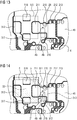
- Fig.1 shows an electrical component 1 according to the prior art in front view, which is suitable for surface mounting on a printed circuit board 2.
- the front functional connection 11 which is in contact with the printed circuit board 2. It is arranged on the underside 13 of the component 1 and at the front side surface 15. The left side surface 17 and the right side surface 18 are not provided with terminals.
- Fig.2 shows the component 1 according to the prior art in side view. It can be seen that the front functional connection 11 extends not only along the front side surface 15 but also a little along the bottom side 13.
- the front functional connection 11 adjoins a switching node 21, to which it is known by means of surface-mounting technology of SMDs and way contacted.
- the switching node 21 is here in a sectional view of the circuit board 2 recognizable and shown schematically, in correct side view, he would not or only slightly recognizable.
- the rear function terminal 12 is also contacted with a conductor track of the printed circuit board 2, wherein this conductor is not shown here.
- the rear functional connector 12 extends over a portion of the rear side surface 16 as well as over a portion of the lower surface 13.
- Fig. 3 shows a component according to the prior art in side view, similar to Fig.2 ,
- the front functional connection 11 and the rear functional connection 12 do not extend over the underside 13, but only over part of the front side surface 15 or the rear side surface 16. They are designed to be somewhat wider than those of FIG Fig.2 and are in contact with the switching node 21 or with a not shown another trace of the circuit board 2 in contact.
- Figure 4 shows a component 1 according to the prior art in plan view. It can be seen the front functional connection 11 and the rear functional connection 12, which protrude beyond the front side surface 15 and the rear side surface 16 of the component 1.
- the front function terminal is in contact with the switching node 21, which has a comparatively large extent on the circuit board 2, and therefore is predestined to emit electromagnetic radiation.
- the switching node 21 further, not shown here components are contacted, which serve to perform a switching function.
- Figure 5 shows a component according to the invention in front view, similar to Fig.1 , It can be seen the electromagnetic shield 3, which extends along the top 14, the left side surface 17 and the right side surface 18 of the component 1, and over parts of the bottom 13.
- a left ground terminal 37 and a right ground terminal 38 provide a connection of the shield 3 to ground potential or another defined potential.
- Other elements in the illustration are the same as Fig. 1 described and will not be explained here.
- Figure 6 shows a component with shielding according to the prior art in side view, similar to Fig.2 , It can be seen the shield 3, which extends over the top 14, but not on the rear side surface 16 or the front side surface 15. In this sectional view, only the right ground terminal 38, which is in the figure behind, recognizable.
- Figure 7 shows a component according to the invention in side view, similar to Figure 6 ,
- the shield 3 has a first projection 31 and a second projection 32.
- the projection 31 protrudes beyond the front side surface 15 so far that it covers the entire surface of the switching node 21 seen in a vertical projection.
- the second projection 32 is arranged symmetrically with respect to the first projection 31 and projects far beyond the node, not shown here, on which the rear functional connection 12 is contacted. This terminal is much smaller than the switching node 21 and therefore would not have required such a shielding.
- the second projection 32 is designed symmetrically to the first projection 31.
- Figure 8 shows a component according to the invention in side view, similar to that of the Figure 7 , Here only one projection 31 of the shield 3 is provided. It is located on the front side surface 15, the switching node 21 outstanding. At the rear side surface 16, the shield 3 is in a region 161 of rear side surface 16 arranged this overlapping. The shield 3 has for this purpose a downwardly extending region 316.
- Figure 9 shows an inventive component 1 in plan view. It can be seen the shield 3 with projection 31, which has a smaller width than the main part of the shield 3. Dashed lines show the body of the component 1, the front functional connection 11 and the rear functional connection 12 and the switching node 21, which are covered by the shield. The circuit board 2 is only partially covered by this. The projection 31 is dimensioned so that it completely covers the switching node 21.
- Figure 10 shows a component according to the invention in plan view similar to Figure 9 ,
- the shield 3 has both a first projection 31 and a second projection 32, which have the same width as the main part of the shield 3.
- the wider here than in Fig. 9 designed switching node 21 is completely covered by the width of the first projection 31.
- Figure 11 shows a component according to the invention in side view.
- the shield 3 consists of a carrier material 35, which is coated with a metal layer 36.
- the coating is shown here only on the upper side of the carrier material 35, according to a variant, not shown, it also extends over its underside and optionally also along the side surfaces 15, 16, 17,18 of the component 1.
- the metal layer 36 is connected to the ground terminal 38th connected and is connected via this with defined potential.
- FIG. 12 shows a circuit diagram detail of a switching power supply 4 according to the invention, which is indicated here only schematically.
- an inductance 5 is provided here. It is connected via the dotted highlighted switching node 21 with a first transistor 41 and a second transistor 42, a diode 43, a capacitor 44 and a test point 45 in connection.
- the interconnect forming the switching node 21 has a large surface, which due to the switching function of the transistors 41, 42 is predestined to emit electromagnetic radiation, which disturbs neighboring components, in particular components adjacent to the switched-mode power supply 4 affected.
- the inductor 5 according to the invention is therefore provided with a shield with projection, which is indicated here in the circuit diagram only symbolically with a T.
- the designation T indicates the T-shaped configuration of the shield with two projections.
- Ground terminal 46, resistor 47 and the other, not shown components of the circuit diagram are not required to understand the invention and will therefore not be described here.
- Figure 13 shows a section of the conductor tracks of a switching power supply according to the invention.
- the tracks are white, the borders between them bold black.
- the position of the inductance 5 of the component 1, the transistors 41, 42, the diode 43 and another component 48 arranged within an integrated circuit 40 are shown by dashed lines.
- the switching node 21 with contact surface 211 for contacting the front functional connection 11, contact surfaces 212 is shown 213, 214 for contacting the integrated circuit 40 and test points 215, 216.
- a contact surface 512 is provided for the rear function connection 12 of the inductance 5, a contact surface 517 for the left ground connection 37, and a contact surface 518 for the right ground connection 38.
- the test point 215 is used to test the switching node 21.
- the test point 216 is also provided for, but is somewhat further objected to by the main surface of the switching node 21. It is not covered by the projection 31 of the shield 3, see also the following figure.
- Figure 14 shows traces accordingly Figure 13 , but here with the representation of the shield 3. Their circumference is shown in phantom, their area hatched. Except for the shield 3 All elements are identical to the previous one.
- the main part 33 of the shield 3 extends substantially above the inductance 5.
- the projection 31 to the right This has a more complex shape than the projections shown in the previous figures.
- the projection 31 has a recess 312, so that the diode 43 is not covered, and thus a visual inspection is accessible.
- the test point 215, however, is covered by the projection 31.
- the test point 216 is not covered and is available for contact with a tester.
- the front portion 313 of the projection 31 has a larger width than its directly adjacent to the main part 33 area.
- the relatively complex shape of the projection 31 shown here is adapted to the existing form of the tracks of the switching node 21.
- a simpler shape of the projection 31 is made possible by the fact that the shape of the switching node 21 and the adjacent interconnects is redesigned, and optionally components such as the diode 43 are arranged slightly offset. If no optical inspection of the diode 43 or corresponding components is required, these can easily be surmounted by the projection 31. This is both not shown here. It is understood that the variants shown above are also modified and can be used according to the invention in another combination.
Landscapes
- Engineering & Computer Science (AREA)
- Microelectronics & Electronic Packaging (AREA)
- Shielding Devices Or Components To Electric Or Magnetic Fields (AREA)
Applications Claiming Priority (1)
| Application Number | Priority Date | Filing Date | Title |
|---|---|---|---|
| DE102016218266.8A DE102016218266A1 (de) | 2016-09-22 | 2016-09-22 | Elektrisches Bauteil |
Publications (3)
| Publication Number | Publication Date |
|---|---|
| EP3300472A2 true EP3300472A2 (fr) | 2018-03-28 |
| EP3300472A3 EP3300472A3 (fr) | 2018-04-04 |
| EP3300472B1 EP3300472B1 (fr) | 2021-07-14 |
Family
ID=59901420
Family Applications (1)
| Application Number | Title | Priority Date | Filing Date |
|---|---|---|---|
| EP17191571.3A Active EP3300472B1 (fr) | 2016-09-22 | 2017-09-18 | Composant électrique |
Country Status (2)
| Country | Link |
|---|---|
| EP (1) | EP3300472B1 (fr) |
| DE (1) | DE102016218266A1 (fr) |
Family Cites Families (2)
| Publication number | Priority date | Publication date | Assignee | Title |
|---|---|---|---|---|
| TWM318903U (en) | 2007-04-03 | 2007-09-11 | Chin-Fu Horng | Electromagnetic shielding device |
| EP2043149A1 (fr) | 2007-09-27 | 2009-04-01 | Oticon A/S | Assemblage comprenant un composant monté en surface à blindage électromagnétique, sa méthode de fabrication et son utilisation |
-
2016
- 2016-09-22 DE DE102016218266.8A patent/DE102016218266A1/de not_active Withdrawn
-
2017
- 2017-09-18 EP EP17191571.3A patent/EP3300472B1/fr active Active
Also Published As
| Publication number | Publication date |
|---|---|
| EP3300472A3 (fr) | 2018-04-04 |
| EP3300472B1 (fr) | 2021-07-14 |
| DE102016218266A1 (de) | 2018-03-22 |
Similar Documents
| Publication | Publication Date | Title |
|---|---|---|
| DE60314353T2 (de) | Leiterplatte und Methode um eine Leiterplatte an einem elektrisch leitenden Gehäuse anzubringen | |
| DE102010008553B4 (de) | Vorrichtung zur Abschirmung eines Elektronikmoduls | |
| EP0866422A2 (fr) | Carte enfichable pour appareils électroniques | |
| DE4327766C2 (de) | Schaltungsanordnung für Kraftfahrzeuge | |
| DE19611785C2 (de) | Elektromagnetische Abschirmvorrichtung für elektronische Geräte | |
| DE112015000298T5 (de) | Steuerung für einen Leistungswandler | |
| DE112018000569T5 (de) | Verbinder | |
| EP3300472B1 (fr) | Composant électrique | |
| DE202006013058U1 (de) | Störstrom-widerstandsfähige Platinenanordnung | |
| DE9300868U1 (de) | Einstückiges Isolierteil, insbesondere Spritzgießteil | |
| DE102017101399A1 (de) | Sensoranordnung | |
| DE112018001014B4 (de) | Elektronische steuervorrichtung | |
| EP0884938B1 (fr) | Unité électronique avec blindage métallique dans une zone de connexions | |
| WO2005024937A1 (fr) | Composant electronique comportant une surface de refroidissement | |
| DE9404817U1 (de) | Leiterplattenanordnung | |
| DE10228981A1 (de) | Vorrichtung zur elektromagnetischen Abschirmung | |
| DE102023122701A1 (de) | Anordnung zum schutz vor elektrostatischer entladung für frequenzumrichter | |
| DE102014109819B4 (de) | Abschirmgehäuse | |
| DE102017204395A1 (de) | Elektronische steuereinheit | |
| DE102020209603A1 (de) | Elektronische steuervorrichtung | |
| DE10336281B3 (de) | Elektrische Baugruppe | |
| DE4302205C2 (de) | Einrichtung zum Reduzieren der Störstrahlung elektrischer Flachbaugruppen | |
| DE102007044338A1 (de) | Steckverbinder mit modifiziertem Isolatorkanal zur Abschirmung elektromagnetischer Strahlung | |
| DE202017100387U1 (de) | Sensoranordnung | |
| WO2008074446A1 (fr) | Composant semi-conducteur |
Legal Events
| Date | Code | Title | Description |
|---|---|---|---|
| PUAI | Public reference made under article 153(3) epc to a published international application that has entered the european phase |
Free format text: ORIGINAL CODE: 0009012 |
|
| STAA | Information on the status of an ep patent application or granted ep patent |
Free format text: STATUS: THE APPLICATION HAS BEEN PUBLISHED |
|
| PUAL | Search report despatched |
Free format text: ORIGINAL CODE: 0009013 |
|
| AK | Designated contracting states |
Kind code of ref document: A2 Designated state(s): AL AT BE BG CH CY CZ DE DK EE ES FI FR GB GR HR HU IE IS IT LI LT LU LV MC MK MT NL NO PL PT RO RS SE SI SK SM TR |
|
| AX | Request for extension of the european patent |
Extension state: BA ME |
|
| AK | Designated contracting states |
Kind code of ref document: A3 Designated state(s): AL AT BE BG CH CY CZ DE DK EE ES FI FR GB GR HR HU IE IS IT LI LT LU LV MC MK MT NL NO PL PT RO RS SE SI SK SM TR |
|
| AX | Request for extension of the european patent |
Extension state: BA ME |
|
| RIC1 | Information provided on ipc code assigned before grant |
Ipc: H01L 23/552 20060101ALI20180227BHEP Ipc: H05K 9/00 20060101AFI20180227BHEP |
|
| STAA | Information on the status of an ep patent application or granted ep patent |
Free format text: STATUS: REQUEST FOR EXAMINATION WAS MADE |
|
| 17P | Request for examination filed |
Effective date: 20181004 |
|
| RBV | Designated contracting states (corrected) |
Designated state(s): AL AT BE BG CH CY CZ DE DK EE ES FI FR GB GR HR HU IE IS IT LI LT LU LV MC MK MT NL NO PL PT RO RS SE SI SK SM TR |
|
| GRAP | Despatch of communication of intention to grant a patent |
Free format text: ORIGINAL CODE: EPIDOSNIGR1 |
|
| STAA | Information on the status of an ep patent application or granted ep patent |
Free format text: STATUS: GRANT OF PATENT IS INTENDED |
|
| INTG | Intention to grant announced |
Effective date: 20210315 |
|
| RIC1 | Information provided on ipc code assigned before grant |
Ipc: H01L 23/552 20060101ALI20210301BHEP Ipc: H05K 9/00 20060101AFI20210301BHEP |
|
| GRAS | Grant fee paid |
Free format text: ORIGINAL CODE: EPIDOSNIGR3 |
|
| GRAA | (expected) grant |
Free format text: ORIGINAL CODE: 0009210 |
|
| STAA | Information on the status of an ep patent application or granted ep patent |
Free format text: STATUS: THE PATENT HAS BEEN GRANTED |
|
| AK | Designated contracting states |
Kind code of ref document: B1 Designated state(s): AL AT BE BG CH CY CZ DE DK EE ES FI FR GB GR HR HU IE IS IT LI LT LU LV MC MK MT NL NO PL PT RO RS SE SI SK SM TR |
|
| REG | Reference to a national code |
Ref country code: GB Ref legal event code: FG4D Free format text: NOT ENGLISH |
|
| REG | Reference to a national code |
Ref country code: IE Ref legal event code: FG4D Free format text: LANGUAGE OF EP DOCUMENT: GERMAN |
|
| REG | Reference to a national code |
Ref country code: DE Ref legal event code: R096 Ref document number: 502017010887 Country of ref document: DE |
|
| REG | Reference to a national code |
Ref country code: AT Ref legal event code: REF Ref document number: 1411705 Country of ref document: AT Kind code of ref document: T Effective date: 20210815 |
|
| REG | Reference to a national code |
Ref country code: LT Ref legal event code: MG9D |
|
| REG | Reference to a national code |
Ref country code: NL Ref legal event code: MP Effective date: 20210714 |
|
| PG25 | Lapsed in a contracting state [announced via postgrant information from national office to epo] |
Ref country code: HR Free format text: LAPSE BECAUSE OF FAILURE TO SUBMIT A TRANSLATION OF THE DESCRIPTION OR TO PAY THE FEE WITHIN THE PRESCRIBED TIME-LIMIT Effective date: 20210714 Ref country code: RS Free format text: LAPSE BECAUSE OF FAILURE TO SUBMIT A TRANSLATION OF THE DESCRIPTION OR TO PAY THE FEE WITHIN THE PRESCRIBED TIME-LIMIT Effective date: 20210714 Ref country code: SE Free format text: LAPSE BECAUSE OF FAILURE TO SUBMIT A TRANSLATION OF THE DESCRIPTION OR TO PAY THE FEE WITHIN THE PRESCRIBED TIME-LIMIT Effective date: 20210714 Ref country code: LT Free format text: LAPSE BECAUSE OF FAILURE TO SUBMIT A TRANSLATION OF THE DESCRIPTION OR TO PAY THE FEE WITHIN THE PRESCRIBED TIME-LIMIT Effective date: 20210714 Ref country code: BG Free format text: LAPSE BECAUSE OF FAILURE TO SUBMIT A TRANSLATION OF THE DESCRIPTION OR TO PAY THE FEE WITHIN THE PRESCRIBED TIME-LIMIT Effective date: 20211014 Ref country code: NL Free format text: LAPSE BECAUSE OF FAILURE TO SUBMIT A TRANSLATION OF THE DESCRIPTION OR TO PAY THE FEE WITHIN THE PRESCRIBED TIME-LIMIT Effective date: 20210714 Ref country code: NO Free format text: LAPSE BECAUSE OF FAILURE TO SUBMIT A TRANSLATION OF THE DESCRIPTION OR TO PAY THE FEE WITHIN THE PRESCRIBED TIME-LIMIT Effective date: 20211014 Ref country code: PT Free format text: LAPSE BECAUSE OF FAILURE TO SUBMIT A TRANSLATION OF THE DESCRIPTION OR TO PAY THE FEE WITHIN THE PRESCRIBED TIME-LIMIT Effective date: 20211115 Ref country code: ES Free format text: LAPSE BECAUSE OF FAILURE TO SUBMIT A TRANSLATION OF THE DESCRIPTION OR TO PAY THE FEE WITHIN THE PRESCRIBED TIME-LIMIT Effective date: 20210714 Ref country code: FI Free format text: LAPSE BECAUSE OF FAILURE TO SUBMIT A TRANSLATION OF THE DESCRIPTION OR TO PAY THE FEE WITHIN THE PRESCRIBED TIME-LIMIT Effective date: 20210714 |
|
| PG25 | Lapsed in a contracting state [announced via postgrant information from national office to epo] |
Ref country code: PL Free format text: LAPSE BECAUSE OF FAILURE TO SUBMIT A TRANSLATION OF THE DESCRIPTION OR TO PAY THE FEE WITHIN THE PRESCRIBED TIME-LIMIT Effective date: 20210714 Ref country code: LV Free format text: LAPSE BECAUSE OF FAILURE TO SUBMIT A TRANSLATION OF THE DESCRIPTION OR TO PAY THE FEE WITHIN THE PRESCRIBED TIME-LIMIT Effective date: 20210714 Ref country code: GR Free format text: LAPSE BECAUSE OF FAILURE TO SUBMIT A TRANSLATION OF THE DESCRIPTION OR TO PAY THE FEE WITHIN THE PRESCRIBED TIME-LIMIT Effective date: 20211015 |
|
| REG | Reference to a national code |
Ref country code: DE Ref legal event code: R097 Ref document number: 502017010887 Country of ref document: DE |
|
| PG25 | Lapsed in a contracting state [announced via postgrant information from national office to epo] |
Ref country code: DK Free format text: LAPSE BECAUSE OF FAILURE TO SUBMIT A TRANSLATION OF THE DESCRIPTION OR TO PAY THE FEE WITHIN THE PRESCRIBED TIME-LIMIT Effective date: 20210714 |
|
| REG | Reference to a national code |
Ref country code: CH Ref legal event code: PL |
|
| PLBE | No opposition filed within time limit |
Free format text: ORIGINAL CODE: 0009261 |
|
| REG | Reference to a national code |
Ref country code: BE Ref legal event code: MM Effective date: 20210930 |
|
| STAA | Information on the status of an ep patent application or granted ep patent |
Free format text: STATUS: NO OPPOSITION FILED WITHIN TIME LIMIT |
|
| PG25 | Lapsed in a contracting state [announced via postgrant information from national office to epo] |
Ref country code: SM Free format text: LAPSE BECAUSE OF FAILURE TO SUBMIT A TRANSLATION OF THE DESCRIPTION OR TO PAY THE FEE WITHIN THE PRESCRIBED TIME-LIMIT Effective date: 20210714 Ref country code: SK Free format text: LAPSE BECAUSE OF FAILURE TO SUBMIT A TRANSLATION OF THE DESCRIPTION OR TO PAY THE FEE WITHIN THE PRESCRIBED TIME-LIMIT Effective date: 20210714 Ref country code: RO Free format text: LAPSE BECAUSE OF FAILURE TO SUBMIT A TRANSLATION OF THE DESCRIPTION OR TO PAY THE FEE WITHIN THE PRESCRIBED TIME-LIMIT Effective date: 20210714 Ref country code: MC Free format text: LAPSE BECAUSE OF FAILURE TO SUBMIT A TRANSLATION OF THE DESCRIPTION OR TO PAY THE FEE WITHIN THE PRESCRIBED TIME-LIMIT Effective date: 20210714 Ref country code: EE Free format text: LAPSE BECAUSE OF FAILURE TO SUBMIT A TRANSLATION OF THE DESCRIPTION OR TO PAY THE FEE WITHIN THE PRESCRIBED TIME-LIMIT Effective date: 20210714 Ref country code: CZ Free format text: LAPSE BECAUSE OF FAILURE TO SUBMIT A TRANSLATION OF THE DESCRIPTION OR TO PAY THE FEE WITHIN THE PRESCRIBED TIME-LIMIT Effective date: 20210714 Ref country code: AL Free format text: LAPSE BECAUSE OF FAILURE TO SUBMIT A TRANSLATION OF THE DESCRIPTION OR TO PAY THE FEE WITHIN THE PRESCRIBED TIME-LIMIT Effective date: 20210714 |
|
| 26N | No opposition filed |
Effective date: 20220419 |
|
| GBPC | Gb: european patent ceased through non-payment of renewal fee |
Effective date: 20211014 |
|
| REG | Reference to a national code |
Ref country code: DE Ref legal event code: R081 Ref document number: 502017010887 Country of ref document: DE Owner name: CONTINENTAL AUTOMOTIVE TECHNOLOGIES GMBH, DE Free format text: FORMER OWNER: CONTINENTAL AUTOMOTIVE GMBH, 30165 HANNOVER, DE Ref country code: DE Ref legal event code: R081 Ref document number: 502017010887 Country of ref document: DE Owner name: AUMOVIO GERMANY GMBH, DE Free format text: FORMER OWNER: CONTINENTAL AUTOMOTIVE GMBH, 30165 HANNOVER, DE |
|
| PG25 | Lapsed in a contracting state [announced via postgrant information from national office to epo] |
Ref country code: LU Free format text: LAPSE BECAUSE OF NON-PAYMENT OF DUE FEES Effective date: 20210918 Ref country code: IT Free format text: LAPSE BECAUSE OF FAILURE TO SUBMIT A TRANSLATION OF THE DESCRIPTION OR TO PAY THE FEE WITHIN THE PRESCRIBED TIME-LIMIT Effective date: 20210714 Ref country code: IE Free format text: LAPSE BECAUSE OF NON-PAYMENT OF DUE FEES Effective date: 20210918 Ref country code: GB Free format text: LAPSE BECAUSE OF NON-PAYMENT OF DUE FEES Effective date: 20211014 Ref country code: BE Free format text: LAPSE BECAUSE OF NON-PAYMENT OF DUE FEES Effective date: 20210930 |
|
| PG25 | Lapsed in a contracting state [announced via postgrant information from national office to epo] |
Ref country code: LI Free format text: LAPSE BECAUSE OF NON-PAYMENT OF DUE FEES Effective date: 20210930 Ref country code: CH Free format text: LAPSE BECAUSE OF NON-PAYMENT OF DUE FEES Effective date: 20210930 |
|
| PG25 | Lapsed in a contracting state [announced via postgrant information from national office to epo] |
Ref country code: HU Free format text: LAPSE BECAUSE OF FAILURE TO SUBMIT A TRANSLATION OF THE DESCRIPTION OR TO PAY THE FEE WITHIN THE PRESCRIBED TIME-LIMIT; INVALID AB INITIO Effective date: 20170918 |
|
| P01 | Opt-out of the competence of the unified patent court (upc) registered |
Effective date: 20230522 |
|
| PG25 | Lapsed in a contracting state [announced via postgrant information from national office to epo] |
Ref country code: CY Free format text: LAPSE BECAUSE OF FAILURE TO SUBMIT A TRANSLATION OF THE DESCRIPTION OR TO PAY THE FEE WITHIN THE PRESCRIBED TIME-LIMIT Effective date: 20210714 |
|
| REG | Reference to a national code |
Ref country code: AT Ref legal event code: MM01 Ref document number: 1411705 Country of ref document: AT Kind code of ref document: T Effective date: 20220918 |
|
| PG25 | Lapsed in a contracting state [announced via postgrant information from national office to epo] |
Ref country code: AT Free format text: LAPSE BECAUSE OF NON-PAYMENT OF DUE FEES Effective date: 20220918 |
|
| REG | Reference to a national code |
Ref country code: DE Ref legal event code: R081 Ref document number: 502017010887 Country of ref document: DE Owner name: CONTINENTAL AUTOMOTIVE TECHNOLOGIES GMBH, DE Free format text: FORMER OWNER: CONTINENTAL AUTOMOTIVE TECHNOLOGIES GMBH, 30165 HANNOVER, DE Ref country code: DE Ref legal event code: R081 Ref document number: 502017010887 Country of ref document: DE Owner name: AUMOVIO GERMANY GMBH, DE Free format text: FORMER OWNER: CONTINENTAL AUTOMOTIVE TECHNOLOGIES GMBH, 30165 HANNOVER, DE |
|
| PG25 | Lapsed in a contracting state [announced via postgrant information from national office to epo] |
Ref country code: MK Free format text: LAPSE BECAUSE OF FAILURE TO SUBMIT A TRANSLATION OF THE DESCRIPTION OR TO PAY THE FEE WITHIN THE PRESCRIBED TIME-LIMIT Effective date: 20210714 |
|
| PG25 | Lapsed in a contracting state [announced via postgrant information from national office to epo] |
Ref country code: MT Free format text: LAPSE BECAUSE OF FAILURE TO SUBMIT A TRANSLATION OF THE DESCRIPTION OR TO PAY THE FEE WITHIN THE PRESCRIBED TIME-LIMIT Effective date: 20210714 |
|
| PGFP | Annual fee paid to national office [announced via postgrant information from national office to epo] |
Ref country code: DE Payment date: 20250930 Year of fee payment: 9 |
|
| PGFP | Annual fee paid to national office [announced via postgrant information from national office to epo] |
Ref country code: FR Payment date: 20250922 Year of fee payment: 9 |
|
| PG25 | Lapsed in a contracting state [announced via postgrant information from national office to epo] |
Ref country code: TR Free format text: LAPSE BECAUSE OF FAILURE TO SUBMIT A TRANSLATION OF THE DESCRIPTION OR TO PAY THE FEE WITHIN THE PRESCRIBED TIME-LIMIT Effective date: 20210714 |
|
| REG | Reference to a national code |
Ref country code: DE Ref legal event code: R081 Ref document number: 502017010887 Country of ref document: DE Owner name: AUMOVIO GERMANY GMBH, DE Free format text: FORMER OWNER: CONTINENTAL AUTOMOTIVE TECHNOLOGIES GMBH, 30175 HANNOVER, DE |