EP3301093A1 - Organische verbindung und organische leuchtdiode und anzeigevorrichtung mit organischer leuchtdiode damit - Google Patents
Organische verbindung und organische leuchtdiode und anzeigevorrichtung mit organischer leuchtdiode damit Download PDFInfo
- Publication number
- EP3301093A1 EP3301093A1 EP17193459.9A EP17193459A EP3301093A1 EP 3301093 A1 EP3301093 A1 EP 3301093A1 EP 17193459 A EP17193459 A EP 17193459A EP 3301093 A1 EP3301093 A1 EP 3301093A1
- Authority
- EP
- European Patent Office
- Prior art keywords
- substituted
- light emitting
- organic light
- organic compound
- emitting diode
- Prior art date
- Legal status (The legal status is an assumption and is not a legal conclusion. Google has not performed a legal analysis and makes no representation as to the accuracy of the status listed.)
- Granted
Links
Images





Classifications
-
- C—CHEMISTRY; METALLURGY
- C07—ORGANIC CHEMISTRY
- C07D—HETEROCYCLIC COMPOUNDS
- C07D401/00—Heterocyclic compounds containing two or more hetero rings, having nitrogen atoms as the only ring hetero atoms, at least one ring being a six-membered ring with only one nitrogen atom
- C07D401/14—Heterocyclic compounds containing two or more hetero rings, having nitrogen atoms as the only ring hetero atoms, at least one ring being a six-membered ring with only one nitrogen atom containing three or more hetero rings
-
- C—CHEMISTRY; METALLURGY
- C07—ORGANIC CHEMISTRY
- C07D—HETEROCYCLIC COMPOUNDS
- C07D405/00—Heterocyclic compounds containing both one or more hetero rings having oxygen atoms as the only ring hetero atoms, and one or more rings having nitrogen as the only ring hetero atom
- C07D405/14—Heterocyclic compounds containing both one or more hetero rings having oxygen atoms as the only ring hetero atoms, and one or more rings having nitrogen as the only ring hetero atom containing three or more hetero rings
-
- C—CHEMISTRY; METALLURGY
- C07—ORGANIC CHEMISTRY
- C07D—HETEROCYCLIC COMPOUNDS
- C07D409/00—Heterocyclic compounds containing two or more hetero rings, at least one ring having sulfur atoms as the only ring hetero atoms
- C07D409/14—Heterocyclic compounds containing two or more hetero rings, at least one ring having sulfur atoms as the only ring hetero atoms containing three or more hetero rings
-
- C—CHEMISTRY; METALLURGY
- C07—ORGANIC CHEMISTRY
- C07F—ACYCLIC, CARBOCYCLIC OR HETEROCYCLIC COMPOUNDS CONTAINING ELEMENTS OTHER THAN CARBON, HYDROGEN, HALOGEN, OXYGEN, NITROGEN, SULFUR, SELENIUM OR TELLURIUM
- C07F7/00—Compounds containing elements of Groups 4 or 14 of the Periodic Table
- C07F7/02—Silicon compounds
- C07F7/08—Compounds having one or more C—Si linkages
- C07F7/0803—Compounds with Si-C or Si-Si linkages
- C07F7/081—Compounds with Si-C or Si-Si linkages comprising at least one atom selected from the elements N, O, halogen, S, Se or Te
- C07F7/0812—Compounds with Si-C or Si-Si linkages comprising at least one atom selected from the elements N, O, halogen, S, Se or Te comprising a heterocyclic ring
- C07F7/0816—Compounds with Si-C or Si-Si linkages comprising at least one atom selected from the elements N, O, halogen, S, Se or Te comprising a heterocyclic ring said ring comprising Si as a ring atom
-
- H—ELECTRICITY
- H10—SEMICONDUCTOR DEVICES; ELECTRIC SOLID-STATE DEVICES NOT OTHERWISE PROVIDED FOR
- H10K—ORGANIC ELECTRIC SOLID-STATE DEVICES
- H10K50/00—Organic light-emitting devices
- H10K50/10—OLEDs or polymer light-emitting diodes [PLED]
- H10K50/19—Tandem OLEDs
-
- H—ELECTRICITY
- H10—SEMICONDUCTOR DEVICES; ELECTRIC SOLID-STATE DEVICES NOT OTHERWISE PROVIDED FOR
- H10K—ORGANIC ELECTRIC SOLID-STATE DEVICES
- H10K59/00—Integrated devices, or assemblies of multiple devices, comprising at least one organic light-emitting element covered by group H10K50/00
- H10K59/10—OLED displays
- H10K59/12—Active-matrix OLED [AMOLED] displays
-
- H—ELECTRICITY
- H10—SEMICONDUCTOR DEVICES; ELECTRIC SOLID-STATE DEVICES NOT OTHERWISE PROVIDED FOR
- H10K—ORGANIC ELECTRIC SOLID-STATE DEVICES
- H10K59/00—Integrated devices, or assemblies of multiple devices, comprising at least one organic light-emitting element covered by group H10K50/00
- H10K59/30—Devices specially adapted for multicolour light emission
- H10K59/38—Devices specially adapted for multicolour light emission comprising colour filters or colour changing media [CCM]
-
- H—ELECTRICITY
- H10—SEMICONDUCTOR DEVICES; ELECTRIC SOLID-STATE DEVICES NOT OTHERWISE PROVIDED FOR
- H10K—ORGANIC ELECTRIC SOLID-STATE DEVICES
- H10K85/00—Organic materials used in the body or electrodes of devices covered by this subclass
- H10K85/40—Organosilicon compounds, e.g. TIPS pentacene
-
- H—ELECTRICITY
- H10—SEMICONDUCTOR DEVICES; ELECTRIC SOLID-STATE DEVICES NOT OTHERWISE PROVIDED FOR
- H10K—ORGANIC ELECTRIC SOLID-STATE DEVICES
- H10K85/00—Organic materials used in the body or electrodes of devices covered by this subclass
- H10K85/60—Organic compounds having low molecular weight
- H10K85/615—Polycyclic condensed aromatic hydrocarbons, e.g. anthracene
-
- H—ELECTRICITY
- H10—SEMICONDUCTOR DEVICES; ELECTRIC SOLID-STATE DEVICES NOT OTHERWISE PROVIDED FOR
- H10K—ORGANIC ELECTRIC SOLID-STATE DEVICES
- H10K85/00—Organic materials used in the body or electrodes of devices covered by this subclass
- H10K85/60—Organic compounds having low molecular weight
- H10K85/615—Polycyclic condensed aromatic hydrocarbons, e.g. anthracene
- H10K85/622—Polycyclic condensed aromatic hydrocarbons, e.g. anthracene containing four rings, e.g. pyrene
-
- H—ELECTRICITY
- H10—SEMICONDUCTOR DEVICES; ELECTRIC SOLID-STATE DEVICES NOT OTHERWISE PROVIDED FOR
- H10K—ORGANIC ELECTRIC SOLID-STATE DEVICES
- H10K85/00—Organic materials used in the body or electrodes of devices covered by this subclass
- H10K85/60—Organic compounds having low molecular weight
- H10K85/649—Aromatic compounds comprising a hetero atom
- H10K85/654—Aromatic compounds comprising a hetero atom comprising only nitrogen as heteroatom
-
- H—ELECTRICITY
- H10—SEMICONDUCTOR DEVICES; ELECTRIC SOLID-STATE DEVICES NOT OTHERWISE PROVIDED FOR
- H10K—ORGANIC ELECTRIC SOLID-STATE DEVICES
- H10K85/00—Organic materials used in the body or electrodes of devices covered by this subclass
- H10K85/60—Organic compounds having low molecular weight
- H10K85/649—Aromatic compounds comprising a hetero atom
- H10K85/657—Polycyclic condensed heteroaromatic hydrocarbons
- H10K85/6572—Polycyclic condensed heteroaromatic hydrocarbons comprising only nitrogen in the heteroaromatic polycondensed ring system, e.g. phenanthroline or carbazole
-
- H—ELECTRICITY
- H10—SEMICONDUCTOR DEVICES; ELECTRIC SOLID-STATE DEVICES NOT OTHERWISE PROVIDED FOR
- H10K—ORGANIC ELECTRIC SOLID-STATE DEVICES
- H10K85/00—Organic materials used in the body or electrodes of devices covered by this subclass
- H10K85/60—Organic compounds having low molecular weight
- H10K85/649—Aromatic compounds comprising a hetero atom
- H10K85/657—Polycyclic condensed heteroaromatic hydrocarbons
- H10K85/6574—Polycyclic condensed heteroaromatic hydrocarbons comprising only oxygen in the heteroaromatic polycondensed ring system, e.g. cumarine dyes
-
- H—ELECTRICITY
- H10—SEMICONDUCTOR DEVICES; ELECTRIC SOLID-STATE DEVICES NOT OTHERWISE PROVIDED FOR
- H10K—ORGANIC ELECTRIC SOLID-STATE DEVICES
- H10K85/00—Organic materials used in the body or electrodes of devices covered by this subclass
- H10K85/60—Organic compounds having low molecular weight
- H10K85/649—Aromatic compounds comprising a hetero atom
- H10K85/657—Polycyclic condensed heteroaromatic hydrocarbons
- H10K85/6576—Polycyclic condensed heteroaromatic hydrocarbons comprising only sulfur in the heteroaromatic polycondensed ring system, e.g. benzothiophene
-
- H—ELECTRICITY
- H10—SEMICONDUCTOR DEVICES; ELECTRIC SOLID-STATE DEVICES NOT OTHERWISE PROVIDED FOR
- H10K—ORGANIC ELECTRIC SOLID-STATE DEVICES
- H10K50/00—Organic light-emitting devices
- H10K50/10—OLEDs or polymer light-emitting diodes [PLED]
- H10K50/11—OLEDs or polymer light-emitting diodes [PLED] characterised by the electroluminescent [EL] layers
- H10K50/125—OLEDs or polymer light-emitting diodes [PLED] characterised by the electroluminescent [EL] layers specially adapted for multicolour light emission, e.g. for emitting white light
- H10K50/13—OLEDs or polymer light-emitting diodes [PLED] characterised by the electroluminescent [EL] layers specially adapted for multicolour light emission, e.g. for emitting white light comprising stacked EL layers within one EL unit
-
- H—ELECTRICITY
- H10—SEMICONDUCTOR DEVICES; ELECTRIC SOLID-STATE DEVICES NOT OTHERWISE PROVIDED FOR
- H10K—ORGANIC ELECTRIC SOLID-STATE DEVICES
- H10K50/00—Organic light-emitting devices
- H10K50/10—OLEDs or polymer light-emitting diodes [PLED]
- H10K50/14—Carrier transporting layers
- H10K50/16—Electron transporting layers
-
- H—ELECTRICITY
- H10—SEMICONDUCTOR DEVICES; ELECTRIC SOLID-STATE DEVICES NOT OTHERWISE PROVIDED FOR
- H10K—ORGANIC ELECTRIC SOLID-STATE DEVICES
- H10K50/00—Organic light-emitting devices
- H10K50/10—OLEDs or polymer light-emitting diodes [PLED]
- H10K50/17—Carrier injection layers
- H10K50/171—Electron injection layers
-
- H—ELECTRICITY
- H10—SEMICONDUCTOR DEVICES; ELECTRIC SOLID-STATE DEVICES NOT OTHERWISE PROVIDED FOR
- H10K—ORGANIC ELECTRIC SOLID-STATE DEVICES
- H10K59/00—Integrated devices, or assemblies of multiple devices, comprising at least one organic light-emitting element covered by group H10K50/00
- H10K59/10—OLED displays
- H10K59/12—Active-matrix OLED [AMOLED] displays
- H10K59/131—Interconnections, e.g. wiring lines or terminals
Definitions
- the present invention relates to an organic compound and more particularly to an organic compound being capable of reducing a driving voltage of an organic light emitting diode and improving an emitting efficiency and a lifetime of the organic light emitting diode and the organic light emitting display device including the organic compound.
- OLED organic light emitting display
- the organic light emitting diode emits light by injecting electrons from a cathode as an electron injection electrode and holes from an anode as a hole injection electrode into an emitting material layer (EML), combining the electrons with the holes, generating an exciton, and transforming the exciton from an excited state to a ground state.
- a flexible substrate for example, a plastic substrate, can be used as a base substrate where elements are formed. Since the OLED device does not require a backlight assembly, the OLED device has low weight and low power consumption. Moreover, the OLED device can be operated at a voltage (e.g., 10V or below) lower than a voltage required to operate other display devices.
- an organic light emitting diode for the OLED device may further include an electron injection layer (EIL) and an electron transporting layer (ETL) between the cathode and the EML.
- EIL electron injection layer
- ETL electron transporting layer
- an alkali halide material e.g., LiF
- an organo-metallic material e.g., lithium quinolate (Liq)
- Liq lithium quinolate
- an alkali metal or an alkali earth metal may be included in the EIL, the alkali metal (or the alkali earth metal) is diffused into the ETL with an electron such that the amount of the alkali metal (or the alkali earth metal) is reduced.
- the amount of the electron from the EIL into the ETL is decreased such that the driving voltage of the organic light emitting diode is increased and the emitting efficiency of the organic light emitting diode is decreased.
- the lifetime of the organic light emitting diode is decreased.
- the present invention is directed to an organic compound and an organic light emitting diode and an organic light emitting display (OLED) device including the same that substantially obviate one or more of the problems due to limitations and disadvantages of the related art.
- An object of the present invention is to provide an organic compound being capable of preventing the decrease of an electron transporting/injection property and the lifetime.
- An object of the present invention is to provide an organic light emitting diode and an OLED device having improved electron transporting/injection property and lifetime.
- an organic compound is , represented by following Formula: , wherein each of R 1 to R 2 is independently selected from the group consisting of hydrogen, substituted or non-substituted C 1 -C 20 alkyl, substituted or non-substituted C 1 -C 20 alkoxy, substituted or non-substituted C 4 -C 30 cycloalkyl, substituted or non-substituted C 4 -C 30 heterocycloalkyl, substituted or non-substituted C 6 -C 60 homoaryl, substituted or non-substituted C 6 -C 60 heteroaryl, substituted or non-substituted C 6 -C 60 homo-oxyaryl and substituted or non-substituted C 6 -C 60 hetero-oxyaryl, wherein each of L 1 and L 2 is independently selected from the group consisting of substituted or non-substituted C 1 -C 20 alkyl, substituted or non-substituted C 1
- an organic light emitting diode comprises the organic compound of the present invention.
- the organic light emitting diode comprises first and second electrodes facing each other; a first emitting part between the first and second electrodes and including a first emitting material layer and an electron transporting layer; a second emitting part between the first emitting part and the second electrode and including a second emitting material layer; and a first charge generation layer between the first and second emitting parts, wherein at least one of the electron transporting layer and the first charge generation layer includes the organic compound.
- an organic light emitting display device comprises a substrate; the above organic light emitting diode: and a thin film transistor between the substrate and the organic light emitting diode and connected to the organic light emitting diode.
- An organic compound of the present invention includes a triazine core (first core) and a bipyridine moiety (second core) directly or indirectly connected (or linked) to the triazine core.
- each of R 1 to R 2 is independently selected from the group consisting of hydrogen, substituted or non-substituted C 1 -C 20 alkyl, substituted or non-substituted C 1 -C 20 alkoxy, substituted or non-substituted C 4 -C 30 cycloalkyl, substituted or non-substituted C 4 -C 30 heterocycloalkyl, substituted or non-substituted C 6 -C 60 homoaryl, substituted or non-substituted C 6 -C 60 heteroaryl, substituted or non-substituted C 6 -C 60 homo-oxyaryl and substituted or non-substituted C 6 -C 60 hetero-oxyaryl.
- each of L 1 and L 2 is independently selected from the group consisting of substituted or non-substituted C 6 -C 60 homoarylene and substituted or non-substituted C 6 -C 60 heteroarylene.
- "m” is 0 (zero) or 1
- "n” is 1 or 2.
- one of X 1 to X 4 and X 9 is nitrogen atom, and the rest of X1 to X 4 and X 9 are CH or CR 3 .
- one of X 5 to X 8 and X 10 is nitrogen atom, and the rest of X 5 to X 8 and X 10 are CH or CR 4 .
- R 3 and R 4 may be independently selected from the group consisting of hydrogen, substituted or non-substituted C 1 -C 20 alkyl, substituted or non-substituted C 1 -C 20 alkoxy, C 1 -C 20 alkyl amino, substituted or non-substituted C 4 -C 30 cycloalkyl, substituted or non-substituted C 4 -C 30 heterocycloalkyl, substituted or non-substituted C 6 -C 60 homoaryl, substituted or non-substituted C 6 -C 60 heteroaryl, substituted or non-substituted C 6 -C 60 homo-oxyaryl and substituted or non-substituted C 6 -C 60 hetero-oxyaryl.
- the substituent may include halogen-substituted or non-substituted alkyl group, halogen-substituted or non-substituted alkoxy group, halogen, cyano group, carboxyl group, carbonyl group, amino group, alkylamino group, nitro group, hydrozyl group, sulfonate group, alkyl silyl group, alkoxy silyl group, cycloakyl silyl group, aryl silyl group, substituted or non-substituted aryl group or heteroaryl group, but it is not limited thereto.
- hetero which is used in heteroaryl, heteroarylene, and so on, means that at least one carbon atom in the aromatic ring or alicyclic ring is substituted by a heteroatom being selected from the group consisting of nitrogen atom (N), oxygen atom (O) and sulfur atom (S).
- each of R 1 , R 2 , R 3 and R 4 may be fused or non-fused homo-aromatic ring, such as phenyl, biphenyl, terphenyl, tetraphenyl, naphtyl, anthracenyl, indenyl, phenalenyl, phenanthrenyl, azulenyl, pyrenyl, fluorenyl, tetracenyl, indacenyl or spiro-fluorenyl, or fused or non-fused hetero-aromatic ring, such as pyrrolyl, pyridyl (or pyridinyl), pyrimidyl (pyrimidinyl), pyrazinyl, pyridazinyl, triazinyl, tetrazinyl, imidazolyl, pyrazolyl
- each of R 1 to R 4 may be independently selected from the group consisting of phenyl, alkylphenyl, biphenyl, alkylbiphenyl, halophenyl, alkoxyphenyl, haloalkoxyphenyl, cyanophenyl, silylphenyl, naphthyl, alkylnaphthyl, halonaphthyl, cyanonaphthyl, silylnaphthyl, phenylnaphthyl, pyridyl, alkylpyridyl, halopyridyl, cyanopyridyl, alkoxypyridyl, silylpyridyl, phenylpyridyl, pyrimidyl, halopyrimidyl, cyanopyridyl, alkoxypyrimidyl, phenylpyrimidyl, quinolinyl,
- the carrier mobility of the organic compound may be controlled by L 1 and L 2 as the linker.
- L 1 and L 2 may be an aromatic linker.
- each of L 1 and L 2 may be one substituted or non-substituted C 6 -C 60 homoarylene and substituted or non-substituted C 6 -C 60 heteroarylene.
- each of L 1 and L 2 may be one substituted or non-substituted C 6 -C 60 homoarylene.
- each of L 1 and L 2 may be independently selected from a group consisting of phenylene, biphenylene, terphenylene, tetraphenylene, indenylene, naphthylene, azulenylene, indacenylene, acenaphthylene, fluorenylene, spiro-fluorenylene, phenalenylene, phenanthrenylene, anthracenylene, fluoranthrenylene, triphenylenylene, pyrenylene, chrysenylene, naphthacenylene, picenylene, perylenylene, pentaphenylene, hexacenylene, pyrrolylene, imidazolylene, pyrazolylene, pyridinylene, pyrazinylene, pyrimidinylene, pyridazinylene, isoindolylene, indolylene, indazolylene, purinylene
- each of L 1 and L 2 may be selected independently from the group consisting of phenylene, alkylphenylene, cyanophenylene, naphthylene, alkylnaphthylene, biphenylene, alkyl biphenylene, anthracenylene, pyrenylene, benzothiophenylene, benzofuranylene, dibenzothiophenylene,arylthiazolylene, dibenzofuranylene, fluorenylene and triphenylene.
- L 1 and L 2 When the number of rings of L 1 and L 2 is increased, the conjugation length of the organic compound is increased such that the energy band gap of the organic compound is decreased. Accordingly, the number of rings of L 1 and L 2 may be 1 to 3.
- L 1 and L 2 may be 5-numbered atom ring to 7-numbered atom ring, and beneficially 6-numbered atom ring.
- each of L 1 and L 2 may phenylene, pyrrolylene, imidazolylene, pyrazolylene, pyrazinylene, pyrimidinylene, pyridazinylene, furanylene or thiophenylene, but it is not limited thereto.
- each of R 1 and R 2 is independently selected from phenyl and biphenyl.
- each of L 1 and L 2 is selected independently from the group consisting of phenylene, naphthylene, biphenylene, anthracenylene, pyrenylene, benzothiophenylene, benzofuranylene, dibenzothiophenylene,arylthiazolylene, dibenzofuranylene, fluorenylene,carbazoylene, 9,9' -dimethyl-fluorenylene, and triphenylene.
- m 0.
- one of X 1 and X 2 is a nitrogen atom and the other of X 1 and X 2 is CH or pyridyl, and X 3 and X 4 are both CH.
- one of X 5 and X 6 is a nitrogen atom and the other of X 5 and X 6 is CH, and X 7 and X 8 are both CH.
- the organic compound in the Formula 1 may be one of materials in Formula 2.
- the organic compound of the present invention includes the triazine core having three nitrogen atoms, each of which have a rich electron property, an electron transporting (or mobility) property of the organic compound is increased such that the electron is efficiently transported by the organic compound.
- the bipyridine moiety which has high electronegativity, is connected (combined or linked) to the triazine core via at least one linker such that the electron transporting property of the organic compound is further increased.
- the triazine core and the bipyridine moiety are separated by the at least one linker, the electron localization problem is prevented such that the electron uniformly exists in the organic compound.
- the electron from a cathode or an N-type charge generation layer (CGL) is efficiently injected or transported into an electron transporting layer (ETL) or an emitting material layer (EML). Accordingly, when the organic compound is used for at least one of an electron injection layer (EIL), the ETL and the N-type CGL of an organic light emitting diode, the electron injection/transporting property in the organic light emitting diode is increased such that there are advantages in the driving voltage, the lifetime and the emitting efficiency.
- the organic compound e.g., the nitrogen atom in the triazine core
- the organic compound e.g., the nitrogen atom in the triazine core
- the nitrogen atom of the triazine core in the organic compound is combined or bonded with the alkali metal or the alkali earth metal as a dopant in the ETL or an N-type CGL to form a gap state
- the electron transporting property of the ETL or the N-type CGL is further improved.
- the organic compound of the present invention includes the triazine core, which has excellent electron transporting/injection property, and the bipyridine moiety, which has excellent electronegativity, connected to the each other via at least one linker. Accordingly, the organic compound is used for a layer of the organic light emitting diode requiring the electron transporting property and/or the electron injection property.
- FIG. 1 is a schematic cross-sectional view of an organic light emitting diode according to a first embodiment of the present invention.
- the organic light emitting diode D1 includes a first electrode 180, a second electrode 184, an organic emitting layer 182 (e.g., an organic material layer or an emitting part) between the first and second electrodes 180 and 184.
- the organic emitting layer 182 includes a hole injection layer (HIL) 210, a hole transporting layer (HTL) 220, an emitting material layer (EML) 230, an electron transporting layer (ETL) 240 and an electron injection layer (EIL) 250 sequentially stacked on the first electrode 180.
- HIL hole injection layer
- HTL hole transporting layer
- EML electron transporting layer
- EIL electron injection layer
- the first electrode 180 is the anode for injecting a hole and includes a high work function conductive material, e.g., indium-tin-oxide (ITO), indium-zinc-oxide (IZO) or zinc oxide (ZnO).
- the second electrode 184 is the cathode for injecting an electron and includes a low work function conductive material, e.g., aluminum (Al), magnesium (Mg) or Al-Mg alloy.
- the HIL 210 is positioned between the first electrode 180 and the HTL 220.
- An interface property between the first electrode 180 of an inorganic material and the HTL 220 of an organic material is improved by the HIL 210.
- the HIL 210 may include one of 4,4',4"-tris(3-methylphenylphenylamino)triphenylamine (MTDATA), copper phthalocyanine (CuPc), tris(4-carbazoyl-9-yl-phenyl)amine (TCTA), N,N'-diphenyl-N,N'-bis(1-naphthyl)-1,1'-biphenyl-4,4"-diamine (NPB or NPD), 1,4,5,8,9,11-hexaazatriphenylenehexacarbonitrile (HATCN), 1,3,5-tris[4-(diphenylamino)phenyl]benzene (TDAPB), poly(3,4-ethylenedioxythiphene)polys
- the HIL 210 may have a thickness of about 1 to 150nm.
- the hole injection property may be improved with the thickness above 1nm, and an increase of the driving voltage resulting from an increase of the thickness of the HIL 210 may be prevented with the thickness below 150nm.
- the HIL 210 may be omitted.
- the HTL 220 is positioned between the HIL 210 and the EML 230.
- the HTL 220 may include a hole transporting material such as N,N'-diphenyl-N,N'-bis(3-methylphenyl)-1,1'-biphenyl-4,4'-diamine (TPD), MTDATA, TCTA, NPD or 4,4'-bis(N-carbazolyl)-1,1'-biphenyl (CBP).
- TPD N,N'-diphenyl-N,N'-bis(3-methylphenyl)-1,1'-biphenyl-4,4'-diamine
- MTDATA MTDATA
- TCTA TCTA
- NPD NPD
- CBP 4,4'-bis(N-carbazolyl)-1,1'-biphenyl
- the HTL 220 may have a double-layered structure of different hole transporting materials.
- the HTL 220 may have a thickness of about 1 to 150nm.
- the hole transporting property may be improved with the thickness above 1nm, and an increase of the driving voltage resulting from an increase of the thickness of the HTL 220 may be prevented with the thickness below 150nm.
- the EML 230 may include a host and a dopant.
- a fluorescent host such as anthracene derivative, pyrene derivative or perylene derivative, and a fluorescent dopant are used for the EML 230.
- the fluorescent host for the EML 230 may be selected from the group consisting of 4,4'-bis(2,2'-diphenylyinyl)-1,1'-biphenyl (DPVBi), 9,10-di-(2-naphtyl)anthracene (ADN), 2,5,8,11-tetra-t-butylperylene (TBADN), 2-tert-butyl-9,10-di(2-naphthyl)anthracene, 2-methyl-9,10-di(2-naphtyl)anthracene (MADN) and 2,2',2"-(1,3,5-benzinetriyl)-tris(1-phenyl-1-H-benzimidazole) (TBPi).
- DPVBi 4,4'-bis(2,2'-diphenylyinyl)-1,1'-biphenyl
- ADN 9,10-di-(2-naphtyl)anthrac
- the fluorescent dopant for the EML 230 may be selected from the group consisting of 4,4'-bis(9-ethyl-3-carbazovinylene)-1,1'-biphenyl (BCzVBi), 2,5,8,11-tetra(tert-butyl)perylene (TBP) and diphenyl-[4-(2-[1,1;4,1]terphenyl-4-yl-vinyl)-phenyl]-amine (BD-1).
- the EML 230 may include a phosphorescent host, e.g., carbazole derivative, and a phosphorescent dopant, e.g., a metal (iridium) complex.
- the dopant may have a weight % of about 1 to about 30 with respect to the host.
- the ETL 240 is positioned between the EML 230 and the second electrode 184, and the EIL 250 is positioned between the ETL 240 and the second electrode 184.
- the ETL 240 may include a derivative of oxadiazole, triazole, phenanthroline, benzoxazole, benzothiazole, benzimidazole and triazine.
- the ETL 240 may include an electron transporting material selected from a group consisting of tris-(8-hydroxyquinoline aluminum (Alq3), 2-biphenyl-4-yl-5-(4-t-butylphenyl)-1,3,4-oxadiazole (PBD), spiro-PBD, Liq, 2-[4-(9,10-Di-2-naphthalenyl-2-anthracenyl)phenyl]-1-phenyl-1H-benzimidazol, 3-(biphenyl-4-yl)-5-(4-tertbutylphenyl)-4-phenyl-4H-1,2,4-triazole (TAZ), 4,7-diphenyl-1,10-phenanthroline (Bphen), tris(phenylquinoxaline (TPQ) and 1,3,5-tris(N-phenylbenzimiazole-2-yl)benzene (TPBI), but it is not limited thereto.
- Alq3 tris-
- the ETL 240 may include the above electron transporting material and the organic compound of the present invention as a dopant.
- the organic compound may have a weight % of about 1 to 30 with respect to the electron transporting material, but it is not limited thereto.
- the ETL 240 may have a thickness of about 1 to 150nm.
- the electron transporting property may be improved with the thickness above 1nm, and an increase of the driving voltage resulting from an increase of the thickness of the ETL 240 may be prevented with the thickness below 150nm.
- the EIL 250 may include the organic compound of the present invention.
- a dopant e.g., an alkali metal or an alkali earth metal, may be doped into the EIL 250 to improve the electron injection property.
- the dopant may have a weight % of about 1 to 20 with respect to the organic compound, but it is not limited thereto.
- the dopant may be one of Li, Na, K, Cs, Mg, Sr, Ba and Ra.
- the dopant may be a metal compound, i.e., an alkali metal compound or an alkali earth metal compound, such as Liq, LiF, NaF, KF, RbF, CsF, FrF, BeF 2 , MgF 2 , CaF 2 , SrF 2 , BaF 2 or RaF 2 .
- the EIL 250 may have a thickness of about 1 to 50nm. The electron injection property may be improved with the thickness above 1nm, and an increase of the driving voltage resulting from an increase of the thickness of the EIL 250 may be prevented with the thickness below 50nm.
- the organic compound of the present invention includes the triazine core having three nitrogen atoms, each of which have a rich electron property, an electron transporting (or mobility) property of the organic compound is increased such that the electron is efficiently transported by the organic compound.
- the bipyridine moiety which has high electronegativity, is connected (combined or linked) to the triazine core via at least one linker such that the electron transporting property of the organic compound is further increased. Accordingly, when the organic compound is used for at least one of the EIL and the ETL of an organic light emitting diode, the electron injection/transporting property into the EML in the organic light emitting diode is increased such that there are advantages in the driving voltage, the lifetime and the emitting efficiency.
- the organic compound of the present invention may be applied to a tandem structure organic light emitting diode emitting the white light.
- the tandem structure white organic light emitting diode may be used for a lighting apparatus, a thin light source, a backlight unit of a liquid crystal display device and a full color display device including a color filter.
- properties of color purity and color stability as well as an emitting efficiency and a lifetime are important facts.
- the white organic light emitting diode may be classified into a single-layered emission structure and a multi-layered emission structure.
- the white organic light emitting diode having a stack structure of at least two emitting parts may be used. This structure may be referred to as the tandem structure.
- FIG. 2 is a schematic cross-sectional view of an organic light emitting diode according to a second embodiment of the present invention.
- the organic light emitting diode D2 which includes two emitting parts, includes a first electrode 180, a second electrode 184, an organic emitting layer 182 between the first and second electrodes 180 and 184 and including first and second emitting parts ST1 and ST2 and a charge generation layer (CGL) 330.
- CGL charge generation layer
- the first electrode 180 is the anode for injecting a hole and includes a high work function conductive material, e.g., ITO, IZO or ZnO.
- the second electrode 184 is the cathode for injecting an electron and includes a low work function conductive material, e.g., Al, Mg or Al-Mg alloy.
- the CGL 330 is positioned between the first and second emitting parts ST1 and ST2. Namely, the first emitting part ST1, the CGL 330 and the second emitting part ST2 are sequentially stacked on the first electrode 180. In other words, the first emitting part ST1 is positioned between the first electrode 180 and the CGL 330, and the second emitting part ST2 is positioned between the second electrode 184 and the CGL 330.
- the first emitting part ST1 may include an HIL 312, a first HTL 314, a first EML 316 and a first ETL 318 sequentially stacked on the first electrode 180.
- the HIL 312 and the first HTL 314 are positioned between the first electrode 180 and the first EML 316.
- the HIL 312 is positioned between the first electrode 180 and the first HTL 314, and the first HTL 314 is positioned between the HIL 312 and the first EML 316.
- the first ETL 318 is positioned between the first EML 316 and the CGL 330.
- the HIL 312 may include at least one selected from the group consisting of MTDATA, CuPc, TCTA, NPD, HATCN, TDAPB), PEDOT/PSS, F4TCNQ and N-(biphenyl-4-yl)-9,9-dimethyl-N-(4-(9-phenyl-9H-carbazole-3-yl)phenyl)-9H-fluorene-2amine.
- the HIL 312 may have a thickness of about 1 to 150nm.
- the hole injection property may be improved with the thickness above 1nm, and an increase of the driving voltage resulting from an increase of the thickness of the HIL 312 may be prevented with the thickness below 150nm.
- the HIL 312 may be omitted according to the structure or property of the organic light emitting diode.
- the first HTL 314 may include at least one selected from a group consisting of TPD, TCTA, MTDATA, NPD and CBP, but it is not limited thereto.
- the first HTL 314 may have a single-layered structure or a multi-layered structure.
- the first HTL 314 may have a thickness of about 1 to 150nm.
- the hole transporting property may be improved with the thickness above 1nm, and an increase of the driving voltage resulting from an increase of the thickness of the first HTL 314 may be prevented with the thickness below 150nm.
- the first EML 316 may be a blue EML.
- the first EML 316 may be a red EML, a green EML or a yellow EML.
- the first EML 316 may be a blue EML, a dark blue EML or a sky blue EML.
- the first EML 316 may be a double-layered structure of the blue EML and the red EML, the blue EML and yellow-green EML, or the blue EML and the green EML.
- the first EML 316 may be a phosphorescent EML including a host, e.g., 4,4'-bis(carbazol-9-yl)biphenyl (CBP), and at least one dopant selected from the group consisting of bis(1-phenylisoquinoline)acetylacetonate iridium (PIQIr(acac), bis(1-phenylquinoline)acetylacetonate iridium(PQIr(acac) and tris(1-phenylquinoline)iridium(PQIr) and octaethylporphyrin platinum (PtOEP), but it is not limited thereto.
- the first EML 316 may be a fluorescent EML including PBD:Eu(DBM) 3 (Phen) or perylene.
- the first emitting part ST1 has an emission peak range of about 600 to 650nm.
- the first EML 316 may be a phosphorescent EML including a host, e.g., CBP, and a dopant of iridium complex, but it is not limited thereto.
- the first EML 316 may a fluorescent EML including tris(8-hydroxyquinolinato)aluminum (Alq 3 ).
- the first emitting part ST1 has an emission peak range of about 510 to 570nm.
- the first EML 316 may be a phosphorescent EML including a host, e.g., CBP, and a dopant of iridium complex, but it is not limited thereto.
- the first EML 316 may a fluorescent EML including spiro-DPVBi, Spiro-CBP, distyryl benzene (DSB), distyryl arene (DSA), PFO-based polymer or PPV-based polymer.
- the first EML 316 may be a sky blue EML or deep blue (dark blue) EML.
- the first emitting part ST1 has an emission peak range of about 440 to 480nm.
- the first emitting part ST1 may include two EMLs.
- the first emitting part ST1 may include the blue EML and the red EML.
- the first emitting part ST1 has an emission peak range of about 440 to 650nm.
- the first EML 316 may have a single-layered structure of the yellow-green EML or a double-layered structure of the yellow-green EML and the green EML.
- the first EML 316 may include at least one host selected from a group consisting of CBP and bis(2-methyl-8-quinolinolate)-4-(phenylphenolato)aluminium (BAlq) and a phosphorescent yellow-green dopant.
- the first emitting part ST 1 has an emission peak range of about 510 to 590nm.
- the first ETL 318 may include an electron transporting material selected from a group consisting of Alq3, PBD, spiro-PBD, Liq, 2-[4-(9,10-Di-2-naphthalenyl-2-anthracenyl)phenyl]-1-phenyl-1H-benzimidazol, TAZ, Bphen, TPQ and TPBI.
- the first ETL 318 may include the above electron transporting material and the organic compound of the present invention as a dopant.
- the first ETL 318 may have a thickness of about 1 to 150nm.
- the electron transporting property may be improved with the thickness above 1nm, and an increase of the driving voltage resulting from an increase of the thickness of the first ETL 318 may be prevented with the thickness below 150nm.
- the second emitting part ST2 may include a second HTL 322, a second EML 324, a second ETL 326 and an EIL 328.
- the second HTL 322 is positioned between the CGL 330 and the second EML 324
- the second ETL 326 is positioned between the second EML 324 and the second electrode 184.
- the EIL 328 is positioned between the second ETL 326 and the second electrode 184.
- the second HTL 322 and the second ETL 326 may be same as or different from the first HTL 314 and the first ETL 318 in the first emitting part ST1, respectively.
- the second EML 324 may be red, green, blue or yellow-green EML.
- the first EML 316 is the blue EML
- the second EML 324 may be yellow-green EML.
- the first EML 316 may be the yellow-green EML
- the second EML 324 may be the blue EML.
- the second EML 324 may have a single-layered structure of the yellow-green EML or a double-layered structure of the yellow-green EML and the green EML.
- the single-layered second EML 324 may include at least one host selected from a group consisting of CBP and bis(2-methyl-8-quinolinolate)-4-(phenylphenolato)aluminium (BAlq) and a phosphorescent yellow-green dopant, but it is not limited thereto.
- the EIL 328 may include an electron injection material being selected from a group consisting of Alq3, PBD, TAZ and BAlq, but it is not limited thereto.
- the EIL 328 may include the organic compound of the present invention.
- the EIL 328 may further include a metal compound as a dopant.
- the dopant may be one of Liq, LiF, NaF, KF, RbF, CsF, FrF, BeF 2 , MgF 2 , CaF 2 , SrF 2 , BaF 2 or RaF 2 , but it is not limited thereto.
- the dopant may have a weight % of about 1 to 20 with respect to the organic compound, but it is not limited thereto.
- the EIL 328 may have a thickness of about 1 to 50nm.
- the electron injection property may be improved with the thickness above 1nm, and an increase of the driving voltage resulting from an increase of the thickness of the EIL 328 may be prevented with the thickness below 50nm.
- the CGL 330 is positioned between the first emitting part ST1 and the second emitting part ST2. Namely, the first and second emitting parts ST1 and ST2 are connected by the CGL 330.
- the CGL 330 may be a P-N junction type CGL including an N-type CGL 330N and a P-type CGL 330P.
- the N-type CGL 330N is positioned between the first ETL 318 and the second HTL 322, and the P-type CGL 330P is positioned between the N-type CGL 330N and the second HTL 322.
- the CGL 330 generates a charge or separates a charge into a hole and an electron such that the hole and the electron are provided into the first and second emitting parts ST1 and ST2.
- the N-type CGL 330N provides the electron into the first ETL 318 of the first emitting part ST1, and the first ETL 318 provide the electron into the first EML 316 of the first emitting part ST 1.
- the P-type CGL 330P provide the hole into the second HTL 322 of the second emitting part ST2, and the second HTL 322 provide the hole into the second EML 324 of the second emitting part ST2.
- the P-type CGL may include an organic material and a dopant, e.g., a metal or a p-type dopant.
- a dopant e.g., a metal or a p-type dopant.
- the metal as the dopant may be selected from the group consisting of Al, Cu, Fe, Pb, Zn, Au, Pt, W, In, Mo, Ni, Ti and their alloy.
- the generally known materials may be used as the p-type dopant and the organic material.
- the p-type dopant may be selected from the group consisting of F 4 -TCNQ, iodine, FeCl 3 , FeF 3 and SbCl 5
- the organic material may be selected from the group consisting of NPB, TPD, N,N,N' ,N' -tetranaphthalenyl-benzidine (TNB) and HAT-CN.
- the tandem structure organic light emitting diode when the electrons are transported from the N-type CGL 330N into the first ETL 318, the driving voltage is increased because of a lowest unoccupied molecular orbital (LUMO) energy level difference between each of the first ETL 318 and the N-type CGL 330N.
- LUMO lowest unoccupied molecular orbital
- at least one of the first ETL 318 and the N-type CGL 330N includes an organic compound of the present invention.
- each of the first ETL 318 and the N-type CGL 330N may further include alkali metal, alkali metal compound, alkali earth metal or alkali earth metal compound as a dopant.
- the electron transporting/injection property may be further improved.
- the organic compound is combined or bonded with the dopant, e.g., alkali metal, alkali metal compound, alkali earth metal or alkali earth metal compound, in the N-type CGL to form a gap state.
- the energy difference between the N-type CGL 330N and the P-type CGL 330P is decreased such that an electron transporting/injection property from the N-type CGL 330N into the first ETL is improved.
- the dopant may be one ofLiq, LiF, NaF, KF, RbF, CsF, FrF, BeF 2 , MgF 2 , CaF 2 , SrF 2 , BaF 2 or RaF 2 , may be doped.
- the dopant may have a weight % of about 1 to 20 with respect to the organic compound, but it is not limited thereto.
- the organic compound of the present invention includes the triazine core having three nitrogen atoms, each of which have a rich electron property, an electron transporting (or mobility) property of the organic compound is increased such that the electron is efficiently transported by the organic compound.
- the bipyridine moiety which has high electronegativity, is connected (combined or linked) to the triazine core via at least one linker such that the electron transporting property of the organic compound is further increased.
- the triazine core and the bipyridine moiety are separated by the at least one linker, the electron localization problem is prevented such that the electron uniformly exists in the organic compound.
- the electron from the N-type CGL is efficiently injected or transported into the ETL.
- the ETL and/or the N-type CGL include the organic compound having the triazine core and bipyridine moiety, the electron injection/transporting property in the organic light emitting diode is increased such that there are advantages in the driving voltage, the lifetime and the emitting efficiency.
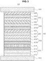
- FIG. 3 is a schematic cross-sectional view of an organic light emitting diode according to a third embodiment of the present invention.
- an organic light emitting diode D3 includes a first electrode 180, a second electrode 184, an organic emitting layer 182 between the first and second electrodes 180 and 184 and including first to third emitting parts ST1, ST2 and ST3 and first and second CGLs 430 and 450.
- first to third emitting parts ST1, ST2 and ST3 and first and second CGLs 430 and 450 may be disposed between the first and second electrodes 180 and 184.
- the first electrode 180 is the anode for injecting a hole and includes a high work function conductive material, e.g., ITO, IZO or ZnO.
- the second electrode 184 is the cathode for injecting an electron and includes a low work function conductive material, e.g., Al, Mg or Al-Mg alloy.
- the first and second CGLs 430 and 450 are positioned between the first and second emitting parts ST1 and ST2 and the second and third emitting parts ST2 and ST3, respectively. Namely, the first emitting part ST1, the first CGL 430, the second emitting part ST2, the second CGL 450 and the third emitting part ST3 are sequentially stacked on the first electrode 180. In other words, the first emitting part ST1 is positioned between the first electrode 180 and the first CGL 430, and the second emitting part ST2 is positioned between the First and Second CGLs 430 and 450. In addition, the third emitting part ST3 is positioned between the second electrode 184 and the second CGL 450.
- the first emitting part ST1 may include an HIL 412, a first HTL 414, a first EML 416 and a first ETL 418 sequentially stacked on the first electrode 180.
- the HIL 412 and the first HTL 414 are positioned between the first electrode 180 and the first EML 416
- the HIL 412 is positioned between the first electrode 180 and the first HTL 414.
- the first ETL 418 is positioned between the first EML 416 and the first CGL 430.
- the HIL 412, the first HTL 414, the first EML 416 and the first ETL 418 may have substantially the same property and structure as those in FIG. 2 .
- the first EML 416 may be a blue EML such that the first emitting part ST1 may have an emission peak range of about 440 to 480nm.
- the second emitting part ST2 may include a second HTL 422, a second EML 424 and a second ETL 426.
- the second HTL 422 is positioned between the first CGL 430 and the second EML 424
- the second ETL 426 is positioned between the second EML 424 and the second CGL 450.
- the second HTL 422, second EML 424 and the second ETL 426 may have substantially the same property and structure as those in FIG. 2 .
- the second EML 424 may be a yellow-green EML such that the second emitting part ST2 may have an emission peak range of about 510 to 590nm.
- the third emitting part ST3 may include a third HTL 442, a third EML 444, a third ETL 446 and an EIL 448.
- the third HTL 442 is positioned between the second CGL 450 and the third EML 444
- the third ETL 446 is positioned between the third EML 444 and the second electrode 184.
- the EIL 448 is positioned between the third ETL 446 and the second electrode 184.
- the third HTL 442, the third ETL 446 and the EIL 448 may have substantially the same property and structure as the second HTL 422, the second ETL 426 and the EIL 428 in FIG. 2 .
- the third EML 444 may have substantially the same property as the first EML 416 or the second EML 424.
- the third EML 444 may be a blue EML such that the third emitting part ST3 may have an emission peak range of about 440 to 480nm.
- the first CGL 430 is positioned between the first emitting part ST1 and the second emitting part ST2, and the second CGL 450 is positioned between the second emitting part ST2 and the third emitting part ST3.
- Each of the first and second CGLs 430 and 450 may be a P-N junction type CGL.
- the first CGL 430 includes an N-type CGL 430N and a P-type CGL 430P
- the second CGL 450 includes an N-type CGL 450N and a P-type CGL 450P.
- the N-type CGL 430N is positioned between the first ETL 418 and the second HTL 422, and the P-type CGL 430P is positioned between the N-type CGL 430N and the second HTL 422.
- the N-type CGL 450N is positioned between the second ETL 426 and the third HTL 442
- the P-type CGL 450P is positioned between the N-type CGL 450N and the third HTL 442.
- Each of the first and second CGLs 430 and 450 generates a charge or separates a charge into a hole and an electron such that the hole and the electron are provided into the first to third emitting parts ST1 to ST3.
- the N-type CGL 430N provides the electron into the first ETL 418 of the first emitting part ST1
- the P-type CGL 430P provide the hole into the second HTL 422 of the second emitting part ST2.
- the N-type CGL 450N provides the electron into the second ETL 426 of the second emitting part ST2
- the P-type CGL 450P provide the hole into the third HTL 442 of the third emitting part ST3.
- Each of the P-type CGLs 430P and 450P may include an organic material and a dopant, e.g., a metal or a p-type dopant.
- a dopant e.g., a metal or a p-type dopant.
- the metal as the dopant may be selected from the group consisting of Al, Cu, Fe, Pb, Zn, Au, Pt, W, In, Mo, Ni, Ti and their alloy.
- the generally known materials may be used as the p-type dopant and the organic material.
- the p-type dopant may be selected from the group consisting of F 4 -TCNQ, iodine, FeCl 3 , FeF 3 and SbCl 5
- the organic material may be selected from the group consisting of NPB, TPD, N,N,N' ,N' -tetranaphthalenyl-benzidine (TNB) and HAT-CN.
- the driving voltage is increased because of a lowest unoccupied molecular orbital (LUMO) energy level difference between each of the first and second ETLs 418 and 426 and each of the N-type CGLs 430N and 450N.
- LUMO lowest unoccupied molecular orbital
- At least one of the first and second ETLs 418 and 426 and the N-type CGLs 430N and 450N includes an organic compound represented in Formula 1 (or Formula 2).
- each of the first and second ETLs 418 and 426 and the N-type CGLs 430N and 450N may further include a dopant, e.g., alkali metal, alkali metal compound, alkali earth metal or alkali earth metal compound.
- the dopant may include one of Liq, LiF, NaF, KF, RbF, CsF, FrF, BeF 2 , MgF 2 , CaF 2 , SrF 2 , BaF 2 and RaF 2 .
- the dopant may have a weight % of about 1 to 20 with respect to the organic compound, but it is not limited thereto.
- the organic compound of the present invention includes the triazine core having three nitrogen atoms, each of which have a rich electron property, an electron transporting (or mobility) property of the organic compound is increased such that the electron is efficiently transported by the organic compound.
- the bipyridine moiety which has high electronegativity, is connected (combined or linked) to the triazine core via at least one linker such that the electron transporting property of the organic compound is further increased.
- the triazine core and the bipyridine moiety are separated by the at least one linker, the electron localization problem is prevented such that the electron uniformly exists in the organic compound.
- the electron from a cathode or an N-type charge generation layer (CGL) is efficiently injected or transported into an electron transporting layer (ETL) or an emitting material layer (EML). Accordingly, when the organic compound is used for at least one of an electron injection layer (EIL), the ETL and the N-type CGL of an organic light emitting diode, the electron injection/transporting property in the organic light emitting diode is increased such that there are advantages in the driving voltage, the lifetime and the emitting efficiency.
- the organic compound of the present invention includes the nitrogen atom having a relatively electron rich sp 2 hybrid orbital, the nitrogen atom in the organic compound is combined or bonded with the dopant, e.g., alkali metal, alkali metal compound, alkali earth metal or alkali earth metal compound, in the N-type CGL to form a gap state.
- the dopant e.g., alkali metal, alkali metal compound, alkali earth metal or alkali earth metal compound
- FIG. 4 is a schematic cross-sectional view of an OLED device according to the present invention.
- an OLED device 100 includes a substrate 110, an organic light emitting diode D over the substrate 110, an encapsulation film 120 covering the organic light emitting diode D.
- a driving thin film transistor (TFT) Td is disposed on the substrate 110, and the organic light emitting diode D is connected to the driving TFT Td.
- a gate line and a data line are disposed on or over the substrate 110 and cross each other to define a pixel region.
- a power line which is parallel to and spaced apart from the gate line or the data line
- a switching TFT which is electrically connected to the gate line and the data line
- a storage capacitor which is connected to the power line and an electrode of the switching TFT may be formed on or over the substrate 110.
- the driving TFT Td is connected to the switching TFT and includes a semiconductor layer 152, a gate electrode 160, a source electrode 170 and a drain electrode 172.
- the semiconductor layer 152 is formed on the substrate 110.
- the semiconductor layer 152 may be formed of an oxide semiconductor material or a poly-silicon.
- a light-shielding pattern (not shown) may be formed under the semiconductor layer 152.
- the light to the semiconductor layer 152 is shielded or blocked by the light-shielding pattern such that thermal degradation of the semiconductor layer 152 can be prevented.
- impurities may be doped into both sides of the semiconductor layer 152.
- a gate insulating layer 154 is formed on the semiconductor layer 152.
- the gate insulating layer 154 may be formed of an inorganic insulating material such as silicon oxide or silicon nitride.
- the gate electrode 160 which is formed of a conductive material, e.g., metal, is formed on the gate insulating layer 154 to correspond to a center of the semiconductor layer 152.
- the gate electrode 160 is connected to the switching TFT.
- An interlayer insulating layer 162 which is formed of an insulating material, is formed on an entire surface of the substrate 110 including the gate electrode 160.
- the interlayer insulating layer 162 may be formed of an inorganic insulating material, e.g., silicon oxide or silicon nitride, or an organic insulating material, e.g., benzocyclobutene or photo-acryl.
- the interlayer insulating layer 162 includes first and second contact holes 164 and 166 exposing both sides of the semiconductor layer 152.
- the first and second contact holes 164 and 166 are positioned at both sides of the gate electrode 160 to be spaced apart from the gate electrode 160.
- the source electrode 170 and the drain electrode 172 which are formed of a conductive material, e.g., metal, are formed on the interlayer insulating layer 162.
- the source electrode 170 and the drain electrode 172 are spaced apart from each other with respect to the gate electrode 160 and respectively contact both sides of the semiconductor layer 152 through the first and second contact holes 164 and 166.
- the source electrode 170 is connected to the power line.
- the gate electrode 160, the source electrode 170 and the drain electrode 172 are positioned over the semiconductor layer 152. Namely, the driving TFT Td has a coplanar structure.
- the gate electrode may be positioned under the semiconductor layer, and the source and drain electrodes may be positioned over the semiconductor layer such that the driving TFT Td may have an inverted staggered structure.
- the semiconductor layer may include amorphous silicon.
- the switching TFT may have substantially the same structure as the driving TFT Td.
- the OLED device 100 may further include a color filter 190.
- the color filter 190 absorbs a part of the red, green and blue light.
- a red color filter pattern, a green color filer pattern and a blue color filter pattern may be disposed in each pixel region. Due to the color filter pattern 190, the OLED device 100 provides a full-color image.
- the color filter 190 is positioned between the light organic emitting diode D and the interlayer insulating layer 162 (or the substrate 110).
- the OLED device 100 is the bottom-emission type.
- the color filter 190 may be positioned on or over the organic light emitting diode D, e.g., over the second electrode 184.
- the color filter 190 may have a thickness of about 2 to 5 micrometers.
- the color filter 190 may be used with the tandem structure white organic light emitting diode D in FIG. 2 or FIG. 3 .
- a passivation layer 174 which includes a drain contact hole 176 exposing the drain electrode 172 of the driving TFT Td, is formed to cover the driving TFT Td and the color filter 190.
- a first electrode 180 which is connected to the drain electrode 172 of the driving TFT Td through the drain contact hole 176, is separately formed on the passivation layer 174 in each pixel region.
- the first electrode 180 may be an anode and may be formed of a conductive material having a relatively high work function.
- the first electrode 180 may be formed of a transparent conductive material such as ITO, IZO or ZnO.
- a reflection electrode or a reflection layer may be formed under the first electrode 180.
- the reflection electrode or the reflection layer may be formed of aluminum (Al), silver (Ag), nickel (Ni) or aluminum-palladium-copper (APC) alloy.
- a bank layer 186 which covers edges of the first electrode 180, is formed on the passivation layer 174.
- the bank 186 exposes a center of the first electrode 180 in the pixel region.
- An organic emitting layer 182 is formed on the first electrode 180.
- the organic emitting layer includes a single emitting part or at least two emitting parts (the tandem structure).
- a second electrode 184 is formed over the substrate 110 including the emitting layer 182.
- the second electrode 184 is positioned at an entire surface of the display area.
- the second electrode 184 may be a cathode and may be formed of a conductive material having a relatively low work function.
- the second electrode 184 may be formed of Al, Mg or Al-Mg alloy.
- the first electrode 180, the emitting layer 182 and the second electrode 184 constitute the organic light emitting diode D.
- the encapsulation film 120 is formed on the organic light emitting diode D to prevent penetration of moisture into the organic light emitting diode D.
- the encapsulation film 120 may has a triple-layered structure of a first inorganic layer, an organic layer and a second inorganic layer. However, it is not limited thereto.
- the organic compound of the present invention includes the triazine core having three nitrogen atoms, each of which have a rich electron property, an electron transporting (or mobility) property of the organic compound is increased such that the electron is efficiently transported by the organic compound.
- the bipyridine moiety which has high electronegativity, is connected (combined or linked) to the triazine core via at least one linker such that the electron transporting property of the organic compound is further increased.
- the nitrogen atom of the triazine core in the organic compound is combined or bonded with the alkali metal or the alkali earth metal as a dopant in the ETL or an N-type CGL to form a gap state, the electron transporting property of the ETL or the N-type CGL is further improved.
- the organic compound when used for at least one of an electron injection layer (EIL), the ETL and the N-type CGL of an organic light emitting diode, the electron injection/transporting property in the organic light emitting diode is increased such that there are advantages in the driving voltage, the lifetime and the emitting efficiency.
- EIL electron injection layer
- the compound A (5g, 9.78mmol), 2-(4-(3-bromophenyl)-6-(pyridin-2-yl)pyridin-2-yl)pyridine (3.15 g, 8.14 mmol), tetrakistriphenylphosphine palladium (0) (Pd(PPh 3 ) 4 ) (0.53 g, 0.46 mmol), 4M potassium carbonate aqueous solution (10 mL), toluene (30 mL) and ethanol (10 mL) were refluxed and stirred for 12 hrs. After completion of the reaction, the distilled water (H 2 O, 50 mL) was added and stirred for 3 hrs.
- the mixture was filtered under the reduced pressure and separated by a column chromatography using methylene chloride (MC) and hexane as an eluent.
- MC methylene chloride
- the resultant was crystallized using MC such that the compound ET_271 (4.88g, yield 86.7%) was obtained.
- An ITO layer is deposited and patterned on a substrate and washed to form the anode (2mm*2mm).
- the substrate is loaded in a vacuum chamber having a base pressure of 5 ⁇ 7*10 -8 , and layers are sequentially deposited as below.
- the compound of Bphen (bathophenanthroline).
- the EL property of the organic light emitting diode in “Example 1" and “Comparative Example 1” is measured using the current supply “KEITHLEY” and the photometer “PR 650" under the room temperature.
- the driving voltage, the external quantum efficiency (EQE) and the lifetime (T95) of the organic light emitting diodes of are measured and listed in Table 1.
- the current density, the EQE and the lifetime (L/L 0 ) are shown in FIGs. 5A to 5C .
- the organic light emitting diode of the present invention (Ex 1) has advantages in the current density, the EQE and the lifetime.
- the organic compound of the present invention includes the triazine core having three nitrogen atoms, each of which have a rich electron property, an electron transporting (or mobility) property of the organic compound is increased such that the electron is efficiently transported by the organic compound.
- the bipyridine moiety which has high electronegativity, is connected (combined or linked) to the triazine core via at least one linker such that the electron transporting property of the organic compound is further increased.
- the triazine core and the bipyridine moiety are separated by the at least one linker, the electron localization problem is prevented such that the electron uniformly exists in the organic compound. Accordingly, when the ETL of the organic light emitting diode includes the organic compound of the present invention, the current from the cathode is efficiently injected into the EML such that there are advantages in the driving voltage, the lifetime and the emitting efficiency.
- An ITO layer is deposited and patterned on a substrate and washed to form the anode (2mm*2mm).
- the substrate is loaded in a vacuum chamber having a base pressure of 5 ⁇ 7*10 -8 , and layers are sequentially deposited as below.
- the compound of ET_243 is used for the first and second N-type CGLs.
- the compound of ET_271 is used for the first and second N-type CGLs.
- the compound of Bphen (bathophenanthroline) is used for the first and second N-type CGLs.
- the EL property of the organic light emitting diode in “Example 2" to “Example 4" and “Comparative Example 2” is measured using the current supply “KEITHLEY” and the photometer “PR 650" under the room temperature.
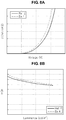
- the driving voltage, the external quantum efficiency (EQE) and the lifetime (T95) of the organic light emitting diodes of are measured and listed in Table 2.
- the current density, the EQE and the lifetime (L/L 0 ) are shown in FIGs. 6A to 6C (comparison of "Ex2" and “Ref 2"), FIGs. 7A to 7C (comparison of "Ex3” and “Ref 2") and FIGs. 8A to 8C (comparison of "Ex4" and “Ref 2").
- the organic compound of the present invention includes the triazine core having three nitrogen atoms, each of which have a rich electron property, an electron transporting (or mobility) property of the organic compound is increased such that the electron is efficiently transported by the organic compound.
- the bipyridine moiety which has high electronegativity, is connected (combined or linked) to the triazine core via at least one linker such that the electron transporting property of the organic compound is further increased.
- the triazine core and the bipyridine moiety are separated by the at least one linker, the electron localization problem is prevented such that the electron uniformly exists in the organic compound. Accordingly, the electron from the cathode or the N-type CGL is efficiently injected into the EML.
- the organic compound of the present invention includes the nitrogen atom having a relatively electron rich sp 2 hybrid orbital
- the nitrogen atom in the organic compound is combined or bonded with the dopant, e.g., alkali metal, alkali metal compound, alkali earth metal or alkali earth metal compound, in the N-type CGL to form a gap state.
- the dopant e.g., alkali metal, alkali metal compound, alkali earth metal or alkali earth metal compound
- the organic compound of the present invention is used for at least one of the EIL, ETL and the N-type CGL, there are advantages in the driving voltage, the lifetime and the emitting efficiency.
Landscapes
- Chemical & Material Sciences (AREA)
- Organic Chemistry (AREA)
- Engineering & Computer Science (AREA)
- Materials Engineering (AREA)
- Physics & Mathematics (AREA)
- Spectroscopy & Molecular Physics (AREA)
- Microelectronics & Electronic Packaging (AREA)
- Optics & Photonics (AREA)
- Electroluminescent Light Sources (AREA)
Applications Claiming Priority (1)
| Application Number | Priority Date | Filing Date | Title |
|---|---|---|---|
| KR1020160125311A KR101944851B1 (ko) | 2016-09-29 | 2016-09-29 | 유기 화합물과 이를 포함하는 유기발광다이오드 및 유기발광 표시장치 |
Publications (2)
| Publication Number | Publication Date |
|---|---|
| EP3301093A1 true EP3301093A1 (de) | 2018-04-04 |
| EP3301093B1 EP3301093B1 (de) | 2020-04-29 |
Family
ID=59974225
Family Applications (1)
| Application Number | Title | Priority Date | Filing Date |
|---|---|---|---|
| EP17193459.9A Active EP3301093B1 (de) | 2016-09-29 | 2017-09-27 | Organische verbindung und organische leuchtdiode und anzeigevorrichtung mit organischer leuchtdiode damit |
Country Status (4)
| Country | Link |
|---|---|
| US (4) | US10468605B2 (de) |
| EP (1) | EP3301093B1 (de) |
| KR (1) | KR101944851B1 (de) |
| CN (1) | CN107880025B (de) |
Cited By (2)
| Publication number | Priority date | Publication date | Assignee | Title |
|---|---|---|---|---|
| EP3480192B1 (de) * | 2017-11-06 | 2020-12-23 | Novaled GmbH | Triazin verbindung und organische halbleitende schicht damit |
| US12324301B2 (en) | 2020-10-29 | 2025-06-03 | Imec Vzw | Contaminated interface mitigation in a semiconductor device |
Families Citing this family (25)
| Publication number | Priority date | Publication date | Assignee | Title |
|---|---|---|---|---|
| KR102523099B1 (ko) * | 2015-06-18 | 2023-04-18 | 엘지디스플레이 주식회사 | 유기전계발광소자 |
| KR102491790B1 (ko) * | 2015-09-25 | 2023-01-26 | 엘지디스플레이 주식회사 | 유기전계발광소자 |
| KR101944851B1 (ko) | 2016-09-29 | 2019-02-01 | 엘지디스플레이 주식회사 | 유기 화합물과 이를 포함하는 유기발광다이오드 및 유기발광 표시장치 |
| CN108424420B (zh) * | 2017-09-30 | 2021-01-12 | 北京绿人科技有限责任公司 | 含有硅原子的三嗪化合物及其应用和一种有机电致发光器件 |
| KR102298231B1 (ko) * | 2017-10-19 | 2021-09-07 | 엘티소재주식회사 | 헤테로고리 화합물 및 이를 이용한 유기 발광 소자 |
| KR102027512B1 (ko) * | 2017-12-22 | 2019-10-01 | 엘지디스플레이 주식회사 | 유기발광다이오드 및 이를 포함하는 유기발광 표시장치 |
| CN111247128B (zh) * | 2018-03-22 | 2023-05-23 | 株式会社Lg化学 | 化合物和包含其的有机发光二极管 |
| JP2021166212A (ja) * | 2018-07-09 | 2021-10-14 | コニカミノルタ株式会社 | 有機エレクトロルミネッセンス素子 |
| KR102238901B1 (ko) | 2018-07-19 | 2021-04-12 | 주식회사 엘지화학 | 유기발광소자 |
| WO2020085319A1 (ja) * | 2018-10-22 | 2020-04-30 | 東ソー株式会社 | 環状アジン化合物、有機電界発光素子用材料、有機電界発光素子用電子輸送材料、及び有機電界発光素子 |
| JP7631663B2 (ja) * | 2018-10-22 | 2025-02-19 | 東ソー株式会社 | 環状アジン化合物、有機電界発光素子用材料、有機電界発光素子用電子輸送材料、及び有機電界発光素子 |
| JP7206816B2 (ja) * | 2018-11-01 | 2023-01-18 | 東ソー株式会社 | 環状アジン化合物、有機電界発光素子用材料、有機電界発光素子用電子輸送材料、及び有機電界発光素子 |
| KR102794030B1 (ko) | 2018-12-14 | 2025-04-09 | 엘지디스플레이 주식회사 | 유기 화합물, 이를 포함하는 유기발광다이오드 및 유기발광표시장치 |
| KR102763275B1 (ko) | 2019-07-15 | 2025-02-10 | 삼성디스플레이 주식회사 | 화합물 및 이를 포함하는 유기 발광 소자 |
| KR20220099948A (ko) * | 2019-11-08 | 2022-07-14 | 이데미쓰 고산 가부시키가이샤 | 유기 일렉트로루미네센스 소자 및 전자 기기 |
| JP2023015412A (ja) * | 2019-11-08 | 2023-02-01 | 出光興産株式会社 | 有機エレクトロルミネッセンス素子及び電子機器 |
| JP7732181B2 (ja) * | 2019-12-02 | 2025-09-02 | 東ソー株式会社 | アジン化合物、そのアジン化合物を有する有機電界発光素子用材料および有機電界発光素子 |
| CN110950852B (zh) * | 2019-12-27 | 2022-12-02 | 吉林奥来德光电材料股份有限公司 | 一种有机电子传输材料及其制备方法和其电致发光器件 |
| JP2023075368A (ja) * | 2020-02-25 | 2023-05-31 | 出光興産株式会社 | 有機エレクトロルミネッセンス素子及び電子機器 |
| CN111718335B (zh) * | 2020-07-03 | 2022-11-18 | 京东方科技集团股份有限公司 | 化合物、有机发光二极管、显示装置 |
| KR102928326B1 (ko) * | 2020-08-26 | 2026-02-19 | 삼성디스플레이 주식회사 | 발광 소자 및 이를 포함하는 전자 장치 |
| KR20220087116A (ko) * | 2020-12-17 | 2022-06-24 | 엘지디스플레이 주식회사 | 유기 금속 화합물, 이를 포함하는 유기발광다이오드 및 유기발광장치 |
| CN114437032B (zh) * | 2021-12-31 | 2023-11-21 | 上海传勤新材料有限公司 | 一种含有四联苯的化合物及其应用 |
| TWI853605B (zh) * | 2022-06-24 | 2024-08-21 | 美商亮銳公司 | 色彩可調式像素之緊湊陣列 |
| CN115117267B (zh) * | 2022-06-29 | 2025-09-09 | 云谷(固安)科技有限公司 | 有机电致发光器件及显示装置 |
Citations (19)
| Publication number | Priority date | Publication date | Assignee | Title |
|---|---|---|---|---|
| EP1930329A1 (de) * | 2005-08-26 | 2008-06-11 | Tosoh Corporation | 1,3,5-triazinderivat, verfahren zur herstellung davon und dieses als komponente enthaltende organische elektrolumineszenzvorrichtung |
| EP2269987A1 (de) * | 2008-02-26 | 2011-01-05 | Hodogaya Chemical Co., Ltd. | Substituierte bipyridylverbindung und organisches elektrolumineszierendes element |
| JP2011126851A (ja) * | 2009-12-21 | 2011-06-30 | Tosoh Corp | 環状アジン誘導体とその製造方法、及びそれらを構成成分とする有機電界発光素子 |
| EP2361909A1 (de) * | 2008-12-01 | 2011-08-31 | Tosoh Corporation | 1,3,5-triazinderivat, herstellungsverfahren dafür und organisches elektrolumineszenzelement damit |
| EP2468731A1 (de) * | 2009-08-21 | 2012-06-27 | Tosoh Corporation | Zyklische azinderivate, herstellungsverfahren dafür und diese als bestandteil enthaltendes organisches elektrolumineszenzelement |
| US20150041789A1 (en) * | 2012-03-22 | 2015-02-12 | Konica Minolta, Inc. | Transparent electrode, electronic device, and organic electroluminescent element |
| WO2016002864A1 (ja) * | 2014-07-01 | 2016-01-07 | 東ソー株式会社 | トリアジン化合物、その製造方法、及びその用途 |
| WO2016024745A2 (ko) * | 2014-08-12 | 2016-02-18 | 삼성에스디아이 주식회사 | 화합물, 이를 포함하는 유기 광전자 소자 및 표시장치 |
| EP3015527A1 (de) * | 2014-10-31 | 2016-05-04 | Samsung SDI Co., Ltd. | Organische verbindung für optoelektrische vorrichtung und zusammensetzung für optoelektrische vorrichtung und organische optoelektrische vorrichtung und anzeigevorrichtung |
| WO2016068441A1 (ko) * | 2014-10-31 | 2016-05-06 | 삼성에스디아이 주식회사 | 유기 광전자 소자 및 표시 장치 |
| US20160141511A1 (en) * | 2014-11-13 | 2016-05-19 | Samsung Display Co., Ltd. | Organic light-emitting device |
| KR20160090262A (ko) * | 2015-01-21 | 2016-07-29 | 주식회사 엘지화학 | 헤테로고리 화합물 및 이를 포함하는 유기 발광 소자 |
| JP2016152239A (ja) * | 2015-02-16 | 2016-08-22 | 東レ株式会社 | 光電変換素子およびそれを用いたイメージセンサ |
| JP2016155795A (ja) * | 2014-07-01 | 2016-09-01 | 東ソー株式会社 | トリアジン化合物、その製造方法、及びその用途 |
| US20160260901A1 (en) * | 2015-03-06 | 2016-09-08 | Samsung Display Co., Ltd. | Organic light-emitting device |
| EP3107131A1 (de) * | 2015-06-18 | 2016-12-21 | LG Display Co., Ltd. | Organische lichtemittierende anzeigevorrichtung |
| US20170092870A1 (en) * | 2015-09-24 | 2017-03-30 | Lg Display Co., Ltd. | Organic light emitting display device |
| US20170092871A1 (en) * | 2015-09-25 | 2017-03-30 | Lg Display Co., Ltd. | Organic light emitting display device |
| CN106892901A (zh) * | 2017-04-21 | 2017-06-27 | 瑞声光电科技(常州)有限公司 | 三嗪化合物及发光器件 |
Family Cites Families (12)
| Publication number | Priority date | Publication date | Assignee | Title |
|---|---|---|---|---|
| US2010128A (en) * | 1931-09-17 | 1935-08-06 | Gerald D Arnold | Centrifugal separator |
| US20130264560A1 (en) * | 2010-12-20 | 2013-10-10 | E I Du Pont De Nemours And Company | Triazine derivatives for electronic applications |
| KR102014168B1 (ko) * | 2012-10-12 | 2019-08-27 | 삼성디스플레이 주식회사 | 유기 발광 소자, 이의 제조 방법 및 물질층 형성 방법 |
| US9997716B2 (en) * | 2014-05-27 | 2018-06-12 | Universal Display Corporation | Organic electroluminescent materials and devices |
| KR102294413B1 (ko) | 2014-11-18 | 2021-08-27 | 삼성디스플레이 주식회사 | 유기발광 표시장치 |
| EP3035400B1 (de) * | 2014-12-17 | 2019-10-23 | Novaled GmbH | Organische Leuchtdiode mit Elektronentransportschichten mit unterschiedlichen Matrixverbindungen |
| EP3093288A1 (de) * | 2015-05-12 | 2016-11-16 | Novaled GmbH | Organische leuchtdiode mit verschiedenen matrixverbindungen in der ersten und der zweiten elektronentransportschicht |
| EP3272832B1 (de) * | 2015-03-16 | 2021-09-15 | LG Chem, Ltd. | Organische lichtemittierende vorrichtung |
| KR101944851B1 (ko) * | 2016-09-29 | 2019-02-01 | 엘지디스플레이 주식회사 | 유기 화합물과 이를 포함하는 유기발광다이오드 및 유기발광 표시장치 |
| EP4164358A1 (de) * | 2017-01-30 | 2023-04-12 | Novaled GmbH | Elektrolumineszenzvorrichtung mit einer definierten schichtanordnung mit einer lichtemittierenden schicht, einer lochtransportschicht und einer elektronentransportschicht |
| JP2018152239A (ja) | 2017-03-13 | 2018-09-27 | 株式会社豊田自動織機 | 電極材料の搬送装置 |
| EP3476915A1 (de) * | 2017-10-30 | 2019-05-01 | Cynora Gmbh | Organische moleküle, insbesondere zur verwendung in opto-elektronischen vorrichtungen |
-
2016
- 2016-09-29 KR KR1020160125311A patent/KR101944851B1/ko active Active
-
2017
- 2017-09-26 CN CN201710881387.XA patent/CN107880025B/zh active Active
- 2017-09-27 US US15/717,414 patent/US10468605B2/en active Active
- 2017-09-27 EP EP17193459.9A patent/EP3301093B1/de active Active
-
2019
- 2019-09-26 US US16/583,990 patent/US11081648B2/en active Active
-
2021
- 2021-06-23 US US17/355,801 patent/US11856846B2/en active Active
-
2023
- 2023-11-15 US US18/510,284 patent/US20240099130A1/en active Pending
Patent Citations (19)
| Publication number | Priority date | Publication date | Assignee | Title |
|---|---|---|---|---|
| EP1930329A1 (de) * | 2005-08-26 | 2008-06-11 | Tosoh Corporation | 1,3,5-triazinderivat, verfahren zur herstellung davon und dieses als komponente enthaltende organische elektrolumineszenzvorrichtung |
| EP2269987A1 (de) * | 2008-02-26 | 2011-01-05 | Hodogaya Chemical Co., Ltd. | Substituierte bipyridylverbindung und organisches elektrolumineszierendes element |
| EP2361909A1 (de) * | 2008-12-01 | 2011-08-31 | Tosoh Corporation | 1,3,5-triazinderivat, herstellungsverfahren dafür und organisches elektrolumineszenzelement damit |
| EP2468731A1 (de) * | 2009-08-21 | 2012-06-27 | Tosoh Corporation | Zyklische azinderivate, herstellungsverfahren dafür und diese als bestandteil enthaltendes organisches elektrolumineszenzelement |
| JP2011126851A (ja) * | 2009-12-21 | 2011-06-30 | Tosoh Corp | 環状アジン誘導体とその製造方法、及びそれらを構成成分とする有機電界発光素子 |
| US20150041789A1 (en) * | 2012-03-22 | 2015-02-12 | Konica Minolta, Inc. | Transparent electrode, electronic device, and organic electroluminescent element |
| JP2016155795A (ja) * | 2014-07-01 | 2016-09-01 | 東ソー株式会社 | トリアジン化合物、その製造方法、及びその用途 |
| WO2016002864A1 (ja) * | 2014-07-01 | 2016-01-07 | 東ソー株式会社 | トリアジン化合物、その製造方法、及びその用途 |
| WO2016024745A2 (ko) * | 2014-08-12 | 2016-02-18 | 삼성에스디아이 주식회사 | 화합물, 이를 포함하는 유기 광전자 소자 및 표시장치 |
| EP3015527A1 (de) * | 2014-10-31 | 2016-05-04 | Samsung SDI Co., Ltd. | Organische verbindung für optoelektrische vorrichtung und zusammensetzung für optoelektrische vorrichtung und organische optoelektrische vorrichtung und anzeigevorrichtung |
| WO2016068441A1 (ko) * | 2014-10-31 | 2016-05-06 | 삼성에스디아이 주식회사 | 유기 광전자 소자 및 표시 장치 |
| US20160141511A1 (en) * | 2014-11-13 | 2016-05-19 | Samsung Display Co., Ltd. | Organic light-emitting device |
| KR20160090262A (ko) * | 2015-01-21 | 2016-07-29 | 주식회사 엘지화학 | 헤테로고리 화합물 및 이를 포함하는 유기 발광 소자 |
| JP2016152239A (ja) * | 2015-02-16 | 2016-08-22 | 東レ株式会社 | 光電変換素子およびそれを用いたイメージセンサ |
| US20160260901A1 (en) * | 2015-03-06 | 2016-09-08 | Samsung Display Co., Ltd. | Organic light-emitting device |
| EP3107131A1 (de) * | 2015-06-18 | 2016-12-21 | LG Display Co., Ltd. | Organische lichtemittierende anzeigevorrichtung |
| US20170092870A1 (en) * | 2015-09-24 | 2017-03-30 | Lg Display Co., Ltd. | Organic light emitting display device |
| US20170092871A1 (en) * | 2015-09-25 | 2017-03-30 | Lg Display Co., Ltd. | Organic light emitting display device |
| CN106892901A (zh) * | 2017-04-21 | 2017-06-27 | 瑞声光电科技(常州)有限公司 | 三嗪化合物及发光器件 |
Non-Patent Citations (1)
| Title |
|---|
| EDWIN C CONSTABLE ET AL: "Metallostars containing {Ru(bpy)3} motifs", INORGANICA CHIMICA, ELSEVIER BV, NL, vol. 300-302, 20 April 2000 (2000-04-20), pages 158 - 168, XP008144990, ISSN: 0020-1693, [retrieved on 20000518], DOI: 10.1016/S0020-1693(99)00483-1 * |
Cited By (3)
| Publication number | Priority date | Publication date | Assignee | Title |
|---|---|---|---|---|
| EP3480192B1 (de) * | 2017-11-06 | 2020-12-23 | Novaled GmbH | Triazin verbindung und organische halbleitende schicht damit |
| US12035622B2 (en) | 2017-11-06 | 2024-07-09 | Novaled Gmbh | Triazine compound and organic semiconductng layer comprising the same |
| US12324301B2 (en) | 2020-10-29 | 2025-06-03 | Imec Vzw | Contaminated interface mitigation in a semiconductor device |
Also Published As
| Publication number | Publication date |
|---|---|
| US20180090686A1 (en) | 2018-03-29 |
| US11856846B2 (en) | 2023-12-26 |
| US11081648B2 (en) | 2021-08-03 |
| KR20180035358A (ko) | 2018-04-06 |
| KR101944851B1 (ko) | 2019-02-01 |
| US20240099130A1 (en) | 2024-03-21 |
| CN107880025B (zh) | 2021-06-15 |
| EP3301093B1 (de) | 2020-04-29 |
| US20210320261A1 (en) | 2021-10-14 |
| CN107880025A (zh) | 2018-04-06 |
| US10468605B2 (en) | 2019-11-05 |
| US20200020864A1 (en) | 2020-01-16 |
Similar Documents
| Publication | Publication Date | Title |
|---|---|---|
| US11856846B2 (en) | Organic compound, and organic light emitting diode and organic light emitting display device including the same | |
| EP3316334B1 (de) | Organische leuchtdiode und anzeigevorrichtung mit organischer leuchtdiode | |
| KR102157756B1 (ko) | 유기 화합물과 이를 포함하는 유기발광다이오드 및 유기발광 표시장치 | |
| US10615347B2 (en) | Organic compound, and organic light emitting diode and organic light emitting display device including the same | |
| US10651396B2 (en) | Organic compound, and organic light emitting diode and organic light emitting display device including the same | |
| US10700290B2 (en) | Organic compound, and organic light-emitting diode and organic light-emitting diode display device including the same | |
| KR102784370B1 (ko) | 유기 화합물과 이를 이용한 발광다이오드 및 유기발광다이오드 표시장치 | |
| KR20200077777A (ko) | 유기 화합물, 이를 포함하는 발광다이오드 및 유기발광장치 | |
| KR102645608B1 (ko) | 유기 화합물, 이를 포함하는 유기발광다이오드 및 유기발광장치 | |
| KR102689354B1 (ko) | 유기 화합물, 이를 포함하는 유기발광다이오드 및 유기발광장치 | |
| KR102642605B1 (ko) | 유기 화합물, 이를 포함하는 유기발광다이오드와 유기발광장치 | |
| KR20190027540A (ko) | 유기 화합물과 이를 포함하는 유기발광다이오드 및 유기발광장치 | |
| KR102515819B1 (ko) | 유기 화합물, 이를 포함하는 유기발광다이오드 및 유기발광장치 | |
| KR20190027537A (ko) | 유기 화합물과 이를 포함하는 유기발광다이오드 및 유기발광장치 | |
| KR102451310B1 (ko) | 유기 화합물, 이를 포함하는 유기발광다이오드 및 유기발광장치 | |
| KR102515820B1 (ko) | 유기 화합물, 이를 포함하는 유기발광다이오드 및 유기발광장치 | |
| KR102686826B1 (ko) | 유기 화합물과 이를 이용한 발광다이오드 및 유기발광다이오드 표시장치 | |
| KR102577042B1 (ko) | 유기 화합물, 이를 포함하는 유기발광다이오드 및 유기발광장치 | |
| KR20250076056A (ko) | 유기발광다이오드 및 이를 포함하는 유기발광장치 |
Legal Events
| Date | Code | Title | Description |
|---|---|---|---|
| PUAI | Public reference made under article 153(3) epc to a published international application that has entered the european phase |
Free format text: ORIGINAL CODE: 0009012 |
|
| STAA | Information on the status of an ep patent application or granted ep patent |
Free format text: STATUS: REQUEST FOR EXAMINATION WAS MADE |
|
| 17P | Request for examination filed |
Effective date: 20170927 |
|
| AK | Designated contracting states |
Kind code of ref document: A1 Designated state(s): AL AT BE BG CH CY CZ DE DK EE ES FI FR GB GR HR HU IE IS IT LI LT LU LV MC MK MT NL NO PL PT RO RS SE SI SK SM TR |
|
| AX | Request for extension of the european patent |
Extension state: BA ME |
|
| RBV | Designated contracting states (corrected) |
Designated state(s): AL AT BE BG CH CY CZ DE DK EE ES FI FR GB GR HR HU IE IS IT LI LT LU LV MC MK MT NL NO PL PT RO RS SE SI SK SM TR |
|
| STAA | Information on the status of an ep patent application or granted ep patent |
Free format text: STATUS: EXAMINATION IS IN PROGRESS |
|
| 17Q | First examination report despatched |
Effective date: 20190405 |
|
| GRAP | Despatch of communication of intention to grant a patent |
Free format text: ORIGINAL CODE: EPIDOSNIGR1 |
|
| STAA | Information on the status of an ep patent application or granted ep patent |
Free format text: STATUS: GRANT OF PATENT IS INTENDED |
|
| INTG | Intention to grant announced |
Effective date: 20191028 |
|
| GRAJ | Information related to disapproval of communication of intention to grant by the applicant or resumption of examination proceedings by the epo deleted |
Free format text: ORIGINAL CODE: EPIDOSDIGR1 |
|
| STAA | Information on the status of an ep patent application or granted ep patent |
Free format text: STATUS: EXAMINATION IS IN PROGRESS |
|
| GRAR | Information related to intention to grant a patent recorded |
Free format text: ORIGINAL CODE: EPIDOSNIGR71 |
|
| GRAS | Grant fee paid |
Free format text: ORIGINAL CODE: EPIDOSNIGR3 |
|
| STAA | Information on the status of an ep patent application or granted ep patent |
Free format text: STATUS: GRANT OF PATENT IS INTENDED |
|
| GRAA | (expected) grant |
Free format text: ORIGINAL CODE: 0009210 |
|
| STAA | Information on the status of an ep patent application or granted ep patent |
Free format text: STATUS: THE PATENT HAS BEEN GRANTED |
|
| INTC | Intention to grant announced (deleted) | ||
| INTG | Intention to grant announced |
Effective date: 20200318 |
|
| AK | Designated contracting states |
Kind code of ref document: B1 Designated state(s): AL AT BE BG CH CY CZ DE DK EE ES FI FR GB GR HR HU IE IS IT LI LT LU LV MC MK MT NL NO PL PT RO RS SE SI SK SM TR |
|
| REG | Reference to a national code |
Ref country code: GB Ref legal event code: FG4D |
|
| REG | Reference to a national code |
Ref country code: CH Ref legal event code: EP |
|
| REG | Reference to a national code |
Ref country code: AT Ref legal event code: REF Ref document number: 1263111 Country of ref document: AT Kind code of ref document: T Effective date: 20200515 |
|
| REG | Reference to a national code |
Ref country code: DE Ref legal event code: R096 Ref document number: 602017015575 Country of ref document: DE |
|
| REG | Reference to a national code |
Ref country code: IE Ref legal event code: FG4D |
|
| REG | Reference to a national code |
Ref country code: NL Ref legal event code: MP Effective date: 20200429 |
|
| REG | Reference to a national code |
Ref country code: LT Ref legal event code: MG4D |
|
| PG25 | Lapsed in a contracting state [announced via postgrant information from national office to epo] |
Ref country code: GR Free format text: LAPSE BECAUSE OF FAILURE TO SUBMIT A TRANSLATION OF THE DESCRIPTION OR TO PAY THE FEE WITHIN THE PRESCRIBED TIME-LIMIT Effective date: 20200730 Ref country code: FI Free format text: LAPSE BECAUSE OF FAILURE TO SUBMIT A TRANSLATION OF THE DESCRIPTION OR TO PAY THE FEE WITHIN THE PRESCRIBED TIME-LIMIT Effective date: 20200429 Ref country code: LT Free format text: LAPSE BECAUSE OF FAILURE TO SUBMIT A TRANSLATION OF THE DESCRIPTION OR TO PAY THE FEE WITHIN THE PRESCRIBED TIME-LIMIT Effective date: 20200429 Ref country code: SE Free format text: LAPSE BECAUSE OF FAILURE TO SUBMIT A TRANSLATION OF THE DESCRIPTION OR TO PAY THE FEE WITHIN THE PRESCRIBED TIME-LIMIT Effective date: 20200429 Ref country code: IS Free format text: LAPSE BECAUSE OF FAILURE TO SUBMIT A TRANSLATION OF THE DESCRIPTION OR TO PAY THE FEE WITHIN THE PRESCRIBED TIME-LIMIT Effective date: 20200829 Ref country code: NO Free format text: LAPSE BECAUSE OF FAILURE TO SUBMIT A TRANSLATION OF THE DESCRIPTION OR TO PAY THE FEE WITHIN THE PRESCRIBED TIME-LIMIT Effective date: 20200729 Ref country code: PT Free format text: LAPSE BECAUSE OF FAILURE TO SUBMIT A TRANSLATION OF THE DESCRIPTION OR TO PAY THE FEE WITHIN THE PRESCRIBED TIME-LIMIT Effective date: 20200831 |
|
| REG | Reference to a national code |
Ref country code: AT Ref legal event code: MK05 Ref document number: 1263111 Country of ref document: AT Kind code of ref document: T Effective date: 20200429 |
|
| PG25 | Lapsed in a contracting state [announced via postgrant information from national office to epo] |
Ref country code: BG Free format text: LAPSE BECAUSE OF FAILURE TO SUBMIT A TRANSLATION OF THE DESCRIPTION OR TO PAY THE FEE WITHIN THE PRESCRIBED TIME-LIMIT Effective date: 20200729 Ref country code: HR Free format text: LAPSE BECAUSE OF FAILURE TO SUBMIT A TRANSLATION OF THE DESCRIPTION OR TO PAY THE FEE WITHIN THE PRESCRIBED TIME-LIMIT Effective date: 20200429 Ref country code: RS Free format text: LAPSE BECAUSE OF FAILURE TO SUBMIT A TRANSLATION OF THE DESCRIPTION OR TO PAY THE FEE WITHIN THE PRESCRIBED TIME-LIMIT Effective date: 20200429 Ref country code: LV Free format text: LAPSE BECAUSE OF FAILURE TO SUBMIT A TRANSLATION OF THE DESCRIPTION OR TO PAY THE FEE WITHIN THE PRESCRIBED TIME-LIMIT Effective date: 20200429 |
|
| PG25 | Lapsed in a contracting state [announced via postgrant information from national office to epo] |
Ref country code: AL Free format text: LAPSE BECAUSE OF FAILURE TO SUBMIT A TRANSLATION OF THE DESCRIPTION OR TO PAY THE FEE WITHIN THE PRESCRIBED TIME-LIMIT Effective date: 20200429 Ref country code: NL Free format text: LAPSE BECAUSE OF FAILURE TO SUBMIT A TRANSLATION OF THE DESCRIPTION OR TO PAY THE FEE WITHIN THE PRESCRIBED TIME-LIMIT Effective date: 20200429 |
|
| PG25 | Lapsed in a contracting state [announced via postgrant information from national office to epo] |
Ref country code: SM Free format text: LAPSE BECAUSE OF FAILURE TO SUBMIT A TRANSLATION OF THE DESCRIPTION OR TO PAY THE FEE WITHIN THE PRESCRIBED TIME-LIMIT Effective date: 20200429 Ref country code: EE Free format text: LAPSE BECAUSE OF FAILURE TO SUBMIT A TRANSLATION OF THE DESCRIPTION OR TO PAY THE FEE WITHIN THE PRESCRIBED TIME-LIMIT Effective date: 20200429 Ref country code: DK Free format text: LAPSE BECAUSE OF FAILURE TO SUBMIT A TRANSLATION OF THE DESCRIPTION OR TO PAY THE FEE WITHIN THE PRESCRIBED TIME-LIMIT Effective date: 20200429 Ref country code: RO Free format text: LAPSE BECAUSE OF FAILURE TO SUBMIT A TRANSLATION OF THE DESCRIPTION OR TO PAY THE FEE WITHIN THE PRESCRIBED TIME-LIMIT Effective date: 20200429 Ref country code: IT Free format text: LAPSE BECAUSE OF FAILURE TO SUBMIT A TRANSLATION OF THE DESCRIPTION OR TO PAY THE FEE WITHIN THE PRESCRIBED TIME-LIMIT Effective date: 20200429 Ref country code: AT Free format text: LAPSE BECAUSE OF FAILURE TO SUBMIT A TRANSLATION OF THE DESCRIPTION OR TO PAY THE FEE WITHIN THE PRESCRIBED TIME-LIMIT Effective date: 20200429 Ref country code: CZ Free format text: LAPSE BECAUSE OF FAILURE TO SUBMIT A TRANSLATION OF THE DESCRIPTION OR TO PAY THE FEE WITHIN THE PRESCRIBED TIME-LIMIT Effective date: 20200429 Ref country code: ES Free format text: LAPSE BECAUSE OF FAILURE TO SUBMIT A TRANSLATION OF THE DESCRIPTION OR TO PAY THE FEE WITHIN THE PRESCRIBED TIME-LIMIT Effective date: 20200429 |
|
| REG | Reference to a national code |
Ref country code: DE Ref legal event code: R097 Ref document number: 602017015575 Country of ref document: DE |
|
| PG25 | Lapsed in a contracting state [announced via postgrant information from national office to epo] |
Ref country code: PL Free format text: LAPSE BECAUSE OF FAILURE TO SUBMIT A TRANSLATION OF THE DESCRIPTION OR TO PAY THE FEE WITHIN THE PRESCRIBED TIME-LIMIT Effective date: 20200429 Ref country code: SK Free format text: LAPSE BECAUSE OF FAILURE TO SUBMIT A TRANSLATION OF THE DESCRIPTION OR TO PAY THE FEE WITHIN THE PRESCRIBED TIME-LIMIT Effective date: 20200429 |
|
| PLBE | No opposition filed within time limit |
Free format text: ORIGINAL CODE: 0009261 |
|
| STAA | Information on the status of an ep patent application or granted ep patent |
Free format text: STATUS: NO OPPOSITION FILED WITHIN TIME LIMIT |
|
| 26N | No opposition filed |
Effective date: 20210201 |
|
| REG | Reference to a national code |
Ref country code: CH Ref legal event code: PL |
|
| PG25 | Lapsed in a contracting state [announced via postgrant information from national office to epo] |
Ref country code: SI Free format text: LAPSE BECAUSE OF FAILURE TO SUBMIT A TRANSLATION OF THE DESCRIPTION OR TO PAY THE FEE WITHIN THE PRESCRIBED TIME-LIMIT Effective date: 20200429 |
|
| REG | Reference to a national code |
Ref country code: BE Ref legal event code: MM Effective date: 20200930 |
|
| PG25 | Lapsed in a contracting state [announced via postgrant information from national office to epo] |
Ref country code: LU Free format text: LAPSE BECAUSE OF NON-PAYMENT OF DUE FEES Effective date: 20200927 |
|
| PG25 | Lapsed in a contracting state [announced via postgrant information from national office to epo] |
Ref country code: BE Free format text: LAPSE BECAUSE OF NON-PAYMENT OF DUE FEES Effective date: 20200930 Ref country code: CH Free format text: LAPSE BECAUSE OF NON-PAYMENT OF DUE FEES Effective date: 20200930 Ref country code: IE Free format text: LAPSE BECAUSE OF NON-PAYMENT OF DUE FEES Effective date: 20200927 Ref country code: LI Free format text: LAPSE BECAUSE OF NON-PAYMENT OF DUE FEES Effective date: 20200930 |
|
| PG25 | Lapsed in a contracting state [announced via postgrant information from national office to epo] |
Ref country code: TR Free format text: LAPSE BECAUSE OF FAILURE TO SUBMIT A TRANSLATION OF THE DESCRIPTION OR TO PAY THE FEE WITHIN THE PRESCRIBED TIME-LIMIT Effective date: 20200429 Ref country code: MT Free format text: LAPSE BECAUSE OF FAILURE TO SUBMIT A TRANSLATION OF THE DESCRIPTION OR TO PAY THE FEE WITHIN THE PRESCRIBED TIME-LIMIT Effective date: 20200429 Ref country code: CY Free format text: LAPSE BECAUSE OF FAILURE TO SUBMIT A TRANSLATION OF THE DESCRIPTION OR TO PAY THE FEE WITHIN THE PRESCRIBED TIME-LIMIT Effective date: 20200429 |
|
| PG25 | Lapsed in a contracting state [announced via postgrant information from national office to epo] |
Ref country code: MK Free format text: LAPSE BECAUSE OF FAILURE TO SUBMIT A TRANSLATION OF THE DESCRIPTION OR TO PAY THE FEE WITHIN THE PRESCRIBED TIME-LIMIT Effective date: 20200429 Ref country code: MC Free format text: LAPSE BECAUSE OF FAILURE TO SUBMIT A TRANSLATION OF THE DESCRIPTION OR TO PAY THE FEE WITHIN THE PRESCRIBED TIME-LIMIT Effective date: 20200429 |
|
| PGFP | Annual fee paid to national office [announced via postgrant information from national office to epo] |
Ref country code: DE Payment date: 20250721 Year of fee payment: 9 |
|
| PGFP | Annual fee paid to national office [announced via postgrant information from national office to epo] |
Ref country code: GB Payment date: 20250722 Year of fee payment: 9 |
|
| PGFP | Annual fee paid to national office [announced via postgrant information from national office to epo] |
Ref country code: FR Payment date: 20250725 Year of fee payment: 9 |