EP3301751A1 - Elektronische vorrichtung mit isolierter antenne - Google Patents
Elektronische vorrichtung mit isolierter antenne Download PDFInfo
- Publication number
- EP3301751A1 EP3301751A1 EP17194574.4A EP17194574A EP3301751A1 EP 3301751 A1 EP3301751 A1 EP 3301751A1 EP 17194574 A EP17194574 A EP 17194574A EP 3301751 A1 EP3301751 A1 EP 3301751A1
- Authority
- EP
- European Patent Office
- Prior art keywords
- pole
- section
- conductive track
- transmission circuit
- track
- Prior art date
- Legal status (The legal status is an assumption and is not a legal conclusion. Google has not performed a legal analysis and makes no representation as to the accuracy of the status listed.)
- Granted
Links
Images





Classifications
-
- H—ELECTRICITY
- H01—ELECTRIC ELEMENTS
- H01P—WAVEGUIDES; RESONATORS, LINES, OR OTHER DEVICES OF THE WAVEGUIDE TYPE
- H01P1/00—Auxiliary devices
- H01P1/20—Frequency-selective devices, e.g. filters
- H01P1/2007—Filtering devices for biasing networks or DC returns
-
- H—ELECTRICITY
- H01—ELECTRIC ELEMENTS
- H01P—WAVEGUIDES; RESONATORS, LINES, OR OTHER DEVICES OF THE WAVEGUIDE TYPE
- H01P1/00—Auxiliary devices
- H01P1/20—Frequency-selective devices, e.g. filters
- H01P1/201—Filters for transverse electromagnetic waves
- H01P1/203—Strip line filters
- H01P1/20327—Electromagnetic interstage coupling
- H01P1/20336—Comb or interdigital filters
- H01P1/20345—Multilayer filters
-
- H—ELECTRICITY
- H01—ELECTRIC ELEMENTS
- H01P—WAVEGUIDES; RESONATORS, LINES, OR OTHER DEVICES OF THE WAVEGUIDE TYPE
- H01P1/00—Auxiliary devices
- H01P1/30—Auxiliary devices for compensation of, or protection against, temperature or moisture effects ; for improving power handling capability
-
- H—ELECTRICITY
- H01—ELECTRIC ELEMENTS
- H01P—WAVEGUIDES; RESONATORS, LINES, OR OTHER DEVICES OF THE WAVEGUIDE TYPE
- H01P5/00—Coupling devices of the waveguide type
- H01P5/12—Coupling devices having more than two ports
- H01P5/16—Conjugate devices, i.e. devices having at least one port decoupled from one other port
- H01P5/18—Conjugate devices, i.e. devices having at least one port decoupled from one other port consisting of two coupled guides, e.g. directional couplers
- H01P5/184—Conjugate devices, i.e. devices having at least one port decoupled from one other port consisting of two coupled guides, e.g. directional couplers the guides being strip lines or microstrips
- H01P5/187—Broadside coupled lines
-
- H—ELECTRICITY
- H01—ELECTRIC ELEMENTS
- H01Q—ANTENNAS, i.e. RADIO AERIALS
- H01Q1/00—Details of, or arrangements associated with, antennas
- H01Q1/12—Supports; Mounting means
- H01Q1/22—Supports; Mounting means by structural association with other equipment or articles
- H01Q1/24—Supports; Mounting means by structural association with other equipment or articles with receiving set
Definitions
- the present invention relates to the protection of users of electronic devices against dangerous voltages.
- the devices more particularly targeted by the invention comprise an external antenna and are for example energy meters, Internet gateways, connected objects (by "IOT” or Internet of Things) ...
- a housing containing a main circuit and a transmission circuit connected to the main circuit and to an external antenna so that the main circuit can process data which is inserted into radio frequency signals received and / or sent. by the transmission circuit.
- the main circuit is likely to receive dangerous voltage to humans, it is necessary to ensure that the antenna itself, which is outside the housing, can be in contact with a user, can not be be subject to said dangerous voltage.
- the isolation comprises optical couplers and / or voltage converters with galvanic isolation connecting the transmission circuit to the main circuit.
- the main disadvantage of this solution is that it is bulky and significantly increases the number of components of the electronic device.
- the frequencies used belong to a wide frequency band and the insulation must be arranged not to attenuate the signal throughout the frequency band used.
- the insulation requirements are very high and impose minimum distances between the parts to isolate them making it almost impossible to use a wound wire transformer.
- An object of the invention is to provide a means for protecting against dangerous voltages the antenna of an electronic device without altering the performance thereof or significantly increase its size.
- an electronic apparatus comprising a housing enclosing a radio frequency signal transmission circuit and an external connection intended to be connected to an external antenna.
- the transmission circuit is connected to the external connection by a coupler comprising at least one pair of a first conductive track and a second conductive track extending on either side of a dielectric having main faces at least partially facing one another to establish between them an electromagnetic transverse wave coupling.
- the first conductive track connects a first pole of the transmission circuit to a second pole of the transmission circuit
- the second conductive track connects a first pole of the external connection to a second pole of the external connection.
- the electronic device comprises a housing 1 enclosing a multilayer printed circuit board 2 (or PCB) on which is formed a main processing circuit, schematized at 3, connected to a radiofrequency signal transmission circuit, schematized 4.
- the transmission circuit 4 is connected by a coupler 5 to an external connection 6 connected to an external antenna 7.
- the transmission circuit 4 is arranged to allow the insertion of data into a signal intended to be transmitted by radio frequency waves via the external antenna 7 or to extract data from a signal received by the external antenna 7 in the form of radiofrequency waves.
- the antenna 7 is also known in itself and connected by a coaxial cable to the connection 6 which comprises a coaxial type connector.
- the coupler 5 comprises at least one pair of a first conductive track, generally designated at 8.1, and a second conductive track, generally designated at 8.2, extending on either side of a substrate or dielectric 9 having main faces (that is to say those of their faces which have the largest area) facing each other to establish between them an electromagnetic transverse wave coupling.
- the conductive track 8.1 is parallel to the conductive track 8.2.
- the conductive tracks are conventionally formed on the printed circuit board 2, the dielectric 9 being formed by a thickness of insulating material of the printed circuit board 2 extending between the conducting track 8.1 and the conducting track 8.2. go. The thickness and the dielectric constant of the dielectric 9 separating the conductive tracks 8.1, 8.2 determine the insulation performance.
- the first conducting track 8.1 comprises a first section 8.11 having a first end connected to a first pole 11 of the transmission circuit 4 and a second end connected by an intermediate section 8.13 at a first end of a second section 8.12 of the first conducting track 8.1 which has a second end connected to a second pole 12 of the transmission circuit 4.
- the second pole 12 of the transmission circuit is of rectangular shape and is not facing the second conductive track 8.2.
- the second pole 12 is here formed by a mass of the transmission circuit 4.
- the connection to the first pole 11 is not represented on the figure 3 it can be realized by a cable extending above the mass of the transmission circuit 4.
- the second conductive track 8.2 has a first section 8.21 having a first end connected to a first pole 21 of the external connection 6 and a second end connected by an intermediate section 8.23 to a first end of a second section 8.22 of the second track 8.2. which has a second end connected to a second pole 22 of the external connection 6.
- the second pole 22 of the connection 6 is of rectangular shape and is not opposite the first conducting track 8.1.
- the second pole 22 is here formed by a mass of the connection 6.
- the connection to the first pole 21 is not represented on the figure 3 it can be realized by a cable extending above the mass of the external connection 6.
- Sections 8.11, 8.12 are parallel to each other and to sections 8.21, 8.22.
- Each section 8.11, 8.12 of the first conducting track 8.1 extends along an axis X facing one of the sections 8.21, 8.22 of the conductive track 8.2 on either side of the dielectric 9.
- the intermediate section 8.13 extends along a Y axis perpendicular to the sections 8.11, 8.12 and does not extend opposite the second pole 22.
- the intermediate section 8.23 is perpendicular to the sections 8.21, 8.22 and does not extend opposite the second pole 12.
- the main faces of the first sections 8.11, 8.21 and the second sections 8.12, 8.22 have a length of 20 mm and a width of 3.5 mm; and the dielectric 9 has a thickness of 600 ⁇ m and a dielectric constant of 4.5.
- Such an arrangement can withstand a voltage of 8000 V while allowing the transmission of signals having frequencies between 700 MHz and 2700 MHz.
- the circulation of a current in the first section 8.11 and the second section 8.12 of the first conductive track 8.1 generates, in the first section 8.21 and the second section 8.22 of the second conducting track 8.2, the circulation of an induced current. of the same value but of opposite sign.
- the flow of a current in the first section 8.21 and the second section 8.22: of the second conductive track 8.2 generates the circulation of an induced current in the first section 8.11 and the second section 8.12 of the first conductive track 8.1.
- the second poles 12, 22 are L-shaped and comprise a first portion 12x, 22x and a second portion 12y, 22y.
- the first portions 12x, 22x extend along the axis X and the second portions 12y, 22y extend along the axis Y.
- a free edge 12a of the second portion 12y of the second pole 12 is connected to the second section 8.12 of the first conductive track 8.1.
- a free edge 22a of the second part 22y of the second pole 22 is connected to the second section 8.22 of the second conductive track 8.2.
- the second poles 12, 22 are not opposite the first and second conductive tracks 8.1, 8.2. More particularly, the free edge 12a is at the overlap limit with the second conductive track 8.2 and the free edge 22a is at the overlap limit with the first conducting track 8.1.
- the second poles 12, 22 are, as previously, L-shaped.
- the difference lies in that the second poles 12, 22 are now partially opposite the first conductive track 8.1 and the second conductive track 8.2. More particularly, the portion 12y of the second pole 12 is completely covered by the second conductive track 8.2, and the portion 22y of the second pole 22 is completely covered by the first conductive track 8.1.
- the figure 6 represents signals S11, S21 of the first poles 11, 21 of the coupler illustrated in FIG. figure 4 .
- the bandwidth at 1dB here ranges from 0.6 to 2.7 GHz (GigaHertz).
- the figure 7 represents signals S11, S21 of the first poles 11, 21 of the coupler illustrated in FIG. figure 5 .
- the bandwidth at 1 dB ranges here from 0.6 to 1.6 GHz (GigaHertz).
- the overlap of the second poles 12, 22 by the first and second conductive tracks 8.1, 8.2 has the effect of reducing the bandwidth of the coupler.
- Tests have shown that, more generally, the larger the overlap of the second portions 12y, 22y of the second poles 12, 22, the smaller the width of the bandwidth of the coupler.
- the width of the bandwidth is optimum when the free edges 12a, 22a are substantially at the overlap limit with respectively the first and second conductive tracks 8.1, 8.2.
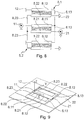
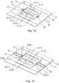
- the first conducting track 8.1 comprises a first section 8.11 and two second sections 8.12 which are parallel to one another as well as to a first section 8.21 and to two second sections 8.22 of the second conducting track 8.2.
- Each section 8.11, 8.12 of the first conducting track 8.1 extends opposite one of the sections 8.21, 8.22 of the conductive track 8.2 on either side of the dielectric 9.
- the first section 8.11 of the first conducting track 8.1 has a first end connected to the first pole 11 of the transmission circuit 4 and a second end connected, by intermediate sections 8.13, to the two second sections 8.12 of the first conducting track 8.1, which are they, connected in parallel to the second pole 12 of the transmission circuit 4.
- the first section 8.21 of the second conductive track 8.2 has a first end connected to the first pole 21 of the external connection 6 and a second end connected by intermediate sections 8.23 at the two second sections 8.22 of the second conductive track 8.2 which are connected in parallel to the second pole 22 of the external connection 6.
- the intermediate sections 8.13 are perpendicular to the sections 8.11, 8.12 and do not extend opposite the second pole 22.
- the intermediate sections 8.23 are perpendicular to the sections 8.21, 8.22.
- the second pole 22 of the connection 6 is here formed by a mass of the connection 6.
- the connection to the first pole He is not represented here on the figure 9 it can be realized by a cable extending above the mass of the transmission circuit 4.
- the main faces of the first sections 8.11, 8.21 and the second sections 8.12, 8.22 have a length of 20 mm and a width of 2.8 mm; and the dielectric 9 has a thickness of 600 ⁇ m and a dielectric constant of 4.5.
- Such an arrangement makes it possible to withstand a voltage of 8000 V while allowing the transmission of signals having frequencies between 1300 MHz and 3100 MHz.
- the second poles 12, 22 are T-shaped and comprise a first portion 12x, 22x and a second portion 12y, 22y.
- the first portions 12x, 22x extend along the axis X and the second portions 12y, 22y extend along the axis Y.
- a free edge 12a of the second portion 12y of the second pole 12 is connected to the second sections 8.12 of the first conductive track 8.1.
- a free edge 22a of the second part 22y of the second pole 22 is connected to the second sections 8.22 of the second conductive track 8.2.
- the second poles 12, 22 are not opposite the first and second conductive tracks 8.1, 8.2. More particularly, the free edge 12a is at the overlap limit with the second conductive track 8.2 and the free edge 22a is at the overlap limit with the first conducting track 8.1.
- the second poles 12, 22 are, as before, T-shaped.
- the difference is that the second poles 12, 22 are now partially facing the first conducting track 8.1 and the second conducting track 8.2. More particularly, the portion 12y of the second pole 12 is completely covered by the second conductive track 8.2, and the portion 22y of the second pole 22 is completely covered by the first conductive track 8.1.
- the figure 12 represents signals S11, S21 of the first poles 11, 21 of the coupler illustrated in FIG. figure 10 .
- the bandwidth at 1 dB ranges here from 0.7 to 3 GHz (GigaHertz).
- the figure 13 represents signals S11, S21 of the first poles 11, 21 of the coupler illustrated in FIG. figure 11 .
- the bandwidth at 1 dB ranges here from 0.7 to 2 GHz (GigaHertz).
- the overlap of the second poles 12, 22 by the first and second conductive tracks 8.1, 8.2 thus has the effect of reducing the bandwidth of the coupler.
- Tests have shown that, more generally, the larger the overlap of the second portions 12y, 22y of the second poles 12, 22, the smaller the width of the bandwidth of the coupler.
- the width of the bandwidth is optimum when the free edges 12a, 22a are substantially at the overlap limit with respectively the first and second conductive tracks 8.1, 8.2.
- the coupler comprises an adaptation capacitor 31 mounted between the first section 8.11 of the first conducting track 8.1 and the second pole 11 of the transmission 4 and an adaptation capacitor 32 mounted between the first section 8.21 of the second conductive track 8.2 and the second pole 21 of the external connection 6.
- the adaptation capacitors 31, 32 serve to compensate for the inductive behavior of the impedance of the coupler at low frequencies: they thus make it possible to increase the bandwidth of the coupler by authorizing the transmission of signals having frequencies between 600 MHz and 3100 MHz.
- the adaptation capacitors 31, 32 are simply, in this first variant, passive components brazed to the poles 11, 21 and sections 8.11, 8.21 concerned.
- the first section 8.11 of the first conducting track 8.1 is connected to the first pole 11 of the transmission circuit 4 via the capacitor 31 and the core of a coaxial cable 41 extending over the ground of the transmission circuit 4 and the first section 8.21 of the second conductive track 8.2 is connected to the first pole 21 by the capacitor 32 and the core of a coaxial cable 42 extending over the ground of the external connection 6.
- the first section 8.11 of the first conducting track 8.1 is connected to the first pole 11 of the transmission circuit 4 by a coplanar conductive track 51 in the ground plane forming the ground of the transmission circuit 4 and the first section 8.21 of the second track Conductor 8.2 is connected to the first pole 21 by a coplanar conducting track 52 in the ground plane forming the ground of the external connection 6.
- the matching capacitors 31, 32 respectively mounted between the first section 8.11 of the first conducting track 8.1 and the first pole 11 of the transmission circuit 4 and between the first section 8.21 of the second conductive track 8.2 and the first pole 21 of the external connection 6 are formed by conductive areas extending in planes parallel to the conductive tracks 8.1, 8.2.
- first end of the first section 8.11 of the first conductive track 8.1 is covered with a layer of dielectric itself covered with a range 61 so as to form a capacitor between said first end and said range 61.
- end of the first section 8.21 of the second conductive track 8.2 is covered with a layer of dielectric itself covered with a range so as to form a capacitor between said first end and said range.
- Said range 61 is then connected to the first pole 11, 21 here by a conductive track, or alternatively by a cable or other.
- the intermediate sections can be replaced by cables.
- One of the matching capacitors may be a passive component and the other a capacitor formed of conductive pads separated from each other by a dielectric.
- the conductive tracks can be connected to the poles directly or indirectly.
- the coupler 5 can be made on the printed circuit board 2 or on a daughter plate attached to the printed circuit board 2 for example to extend parallel or perpendicular to it.
- the electronic circuit of the apparatus may be different from that described.
Landscapes
- Physics & Mathematics (AREA)
- Electromagnetism (AREA)
- Near-Field Transmission Systems (AREA)
- Transmitters (AREA)
- Details Of Aerials (AREA)
Applications Claiming Priority (1)
| Application Number | Priority Date | Filing Date | Title |
|---|---|---|---|
| FR1659527A FR3057111B1 (fr) | 2016-10-03 | 2016-10-03 | Dispositif electronique a antenne isolee |
Publications (2)
| Publication Number | Publication Date |
|---|---|
| EP3301751A1 true EP3301751A1 (de) | 2018-04-04 |
| EP3301751B1 EP3301751B1 (de) | 2020-08-19 |
Family
ID=57860993
Family Applications (1)
| Application Number | Title | Priority Date | Filing Date |
|---|---|---|---|
| EP17194574.4A Active EP3301751B1 (de) | 2016-10-03 | 2017-10-03 | Elektronische vorrichtung mit isolierter antenne |
Country Status (2)
| Country | Link |
|---|---|
| EP (1) | EP3301751B1 (de) |
| FR (1) | FR3057111B1 (de) |
Citations (4)
| Publication number | Priority date | Publication date | Assignee | Title |
|---|---|---|---|---|
| US6018277A (en) * | 1997-03-20 | 2000-01-25 | Nokia Mobile Phones Limited | Series of strip lines for phasing and balancing a signal |
| US20070024398A1 (en) * | 2005-07-28 | 2007-02-01 | Tdk Corporation | Electronic device and filter |
| US20070229368A1 (en) * | 2004-08-27 | 2007-10-04 | Hiroshi Hata | Planar coupler and integrated antenna system |
| US7421265B1 (en) * | 2005-03-04 | 2008-09-02 | Cisco Technology, Inc. | Selectable network antenna systems and methods |
-
2016
- 2016-10-03 FR FR1659527A patent/FR3057111B1/fr not_active Expired - Fee Related
-
2017
- 2017-10-03 EP EP17194574.4A patent/EP3301751B1/de active Active
Patent Citations (4)
| Publication number | Priority date | Publication date | Assignee | Title |
|---|---|---|---|---|
| US6018277A (en) * | 1997-03-20 | 2000-01-25 | Nokia Mobile Phones Limited | Series of strip lines for phasing and balancing a signal |
| US20070229368A1 (en) * | 2004-08-27 | 2007-10-04 | Hiroshi Hata | Planar coupler and integrated antenna system |
| US7421265B1 (en) * | 2005-03-04 | 2008-09-02 | Cisco Technology, Inc. | Selectable network antenna systems and methods |
| US20070024398A1 (en) * | 2005-07-28 | 2007-02-01 | Tdk Corporation | Electronic device and filter |
Also Published As
| Publication number | Publication date |
|---|---|
| EP3301751B1 (de) | 2020-08-19 |
| FR3057111B1 (fr) | 2020-10-30 |
| FR3057111A1 (fr) | 2018-04-06 |
Similar Documents
| Publication | Publication Date | Title |
|---|---|---|
| EP1863116B1 (de) | Breitbandrichtkoppler | |
| EP1427053B1 (de) | Richtkoppler | |
| US10178762B2 (en) | Device and method for transmitting differential data signals | |
| FR2778272A1 (fr) | Dispositif de radiocommunication et antenne bifrequence realisee selon la technique des microrubans | |
| EP0201409A1 (de) | Breitbandiger Richtungskoppler für einen Mikrostreifenleiter | |
| FR2467488A1 (fr) | Dispositif combinateur/diviseur micro-ondes a trois voies, adapte pour des resistances d'isolement externes | |
| FR2762729A1 (fr) | Diviseur de puissance rf | |
| FR2578104A1 (fr) | Filtre passe-bande pour hyperfrequences | |
| EP2178152A1 (de) | Elektronische Umschaltvorrichtung für Hochfrequenzsignale | |
| FR2549283A1 (fr) | Transformateur d'impedance, a large bande, de rapport de transformation voisin de trois, pour radiofrequences | |
| EP0023873B1 (de) | Passiver Leistungsbegrenzer mit Halbleitern und als Streifenleitung ausgeführt und Mikrowellenschaltung mit einem solchen Begrenzer | |
| EP0467818B1 (de) | Übergangsstück zwischen elektromagnetischen Hohlleitern, insbesondere zwischen einem Rundhohlleiter und einem Koaxialhohlleiter | |
| FR2643749A1 (fr) | Dispositif de couplage d'une ligne coaxiale a haute frequence | |
| EP3301751B1 (de) | Elektronische vorrichtung mit isolierter antenne | |
| EP0078188A1 (de) | Breitband-Hochfrequenzanordnung zur Erzeugung von harmonischer gerader Ordnung eines Eingangssignals und deren Verwendung in einem H.F.-System | |
| FR2806534A1 (fr) | Dispositif a circuit non reciproque et appareil a circuit haute frequence l'incorporant | |
| EP0073165B1 (de) | Mikrowellenschalter | |
| EP3605734B1 (de) | Antennevorrichtung umfassend mindestens zwei antennen und electrische verbindung auf gleichem substrat | |
| EP0790503B1 (de) | Hochfrequenz-Leistungsmesseinrichtung | |
| EP0223673A1 (de) | Kopplungsvorrichtung zwischen einer Übertragungsleitung elektromagnetischer Oberflächenwellen und einer Mikrostreifenleitung | |
| EP0420337A1 (de) | Balancierter Hochfrequenzmischer mit Symmetrierschaltung | |
| FR2570904A1 (fr) | Dispositif de protection pour sortie d'emetteur | |
| EP3376515B1 (de) | Hyperfrequenz-schaltvorrichtung mit ablesung durch fernmessung des zustands der eingangs- und ausgangsanschlüsse | |
| EP0100274B1 (de) | Anpassungs- und Einweganordnung mit Ferritzirkulator | |
| FR3146031A1 (fr) | Antenne passive incorporant un cadre blindé |
Legal Events
| Date | Code | Title | Description |
|---|---|---|---|
| PUAI | Public reference made under article 153(3) epc to a published international application that has entered the european phase |
Free format text: ORIGINAL CODE: 0009012 |
|
| STAA | Information on the status of an ep patent application or granted ep patent |
Free format text: STATUS: THE APPLICATION HAS BEEN PUBLISHED |
|
| AK | Designated contracting states |
Kind code of ref document: A1 Designated state(s): AL AT BE BG CH CY CZ DE DK EE ES FI FR GB GR HR HU IE IS IT LI LT LU LV MC MK MT NL NO PL PT RO RS SE SI SK SM TR |
|
| AX | Request for extension of the european patent |
Extension state: BA ME |
|
| STAA | Information on the status of an ep patent application or granted ep patent |
Free format text: STATUS: REQUEST FOR EXAMINATION WAS MADE |
|
| 17P | Request for examination filed |
Effective date: 20181004 |
|
| RBV | Designated contracting states (corrected) |
Designated state(s): AL AT BE BG CH CY CZ DE DK EE ES FI FR GB GR HR HU IE IS IT LI LT LU LV MC MK MT NL NO PL PT RO RS SE SI SK SM TR |
|
| STAA | Information on the status of an ep patent application or granted ep patent |
Free format text: STATUS: EXAMINATION IS IN PROGRESS |
|
| 17Q | First examination report despatched |
Effective date: 20190319 |
|
| REG | Reference to a national code |
Ref country code: DE Ref legal event code: R079 Ref document number: 602017021836 Country of ref document: DE Free format text: PREVIOUS MAIN CLASS: H01P0001200000 Ipc: H01Q0001240000 |
|
| RIC1 | Information provided on ipc code assigned before grant |
Ipc: H01P 5/18 20060101ALI20200212BHEP Ipc: H01P 1/20 20060101ALI20200212BHEP Ipc: H01P 1/203 20060101ALI20200212BHEP Ipc: H01P 1/30 20060101ALI20200212BHEP Ipc: H01Q 1/24 20060101AFI20200212BHEP |
|
| GRAP | Despatch of communication of intention to grant a patent |
Free format text: ORIGINAL CODE: EPIDOSNIGR1 |
|
| STAA | Information on the status of an ep patent application or granted ep patent |
Free format text: STATUS: GRANT OF PATENT IS INTENDED |
|
| INTG | Intention to grant announced |
Effective date: 20200325 |
|
| RIN1 | Information on inventor provided before grant (corrected) |
Inventor name: TISNE, ALAIN |
|
| GRAS | Grant fee paid |
Free format text: ORIGINAL CODE: EPIDOSNIGR3 |
|
| GRAA | (expected) grant |
Free format text: ORIGINAL CODE: 0009210 |
|
| STAA | Information on the status of an ep patent application or granted ep patent |
Free format text: STATUS: THE PATENT HAS BEEN GRANTED |
|
| AK | Designated contracting states |
Kind code of ref document: B1 Designated state(s): AL AT BE BG CH CY CZ DE DK EE ES FI FR GB GR HR HU IE IS IT LI LT LU LV MC MK MT NL NO PL PT RO RS SE SI SK SM TR |
|
| REG | Reference to a national code |
Ref country code: CH Ref legal event code: EP |
|
| REG | Reference to a national code |
Ref country code: DE Ref legal event code: R096 Ref document number: 602017021836 Country of ref document: DE |
|
| REG | Reference to a national code |
Ref country code: AT Ref legal event code: REF Ref document number: 1305001 Country of ref document: AT Kind code of ref document: T Effective date: 20200915 |
|
| REG | Reference to a national code |
Ref country code: IE Ref legal event code: FG4D Free format text: LANGUAGE OF EP DOCUMENT: FRENCH |
|
| REG | Reference to a national code |
Ref country code: LT Ref legal event code: MG4D |
|
| REG | Reference to a national code |
Ref country code: NL Ref legal event code: MP Effective date: 20200819 |
|
| PG25 | Lapsed in a contracting state [announced via postgrant information from national office to epo] |
Ref country code: HR Free format text: LAPSE BECAUSE OF FAILURE TO SUBMIT A TRANSLATION OF THE DESCRIPTION OR TO PAY THE FEE WITHIN THE PRESCRIBED TIME-LIMIT Effective date: 20200819 Ref country code: LT Free format text: LAPSE BECAUSE OF FAILURE TO SUBMIT A TRANSLATION OF THE DESCRIPTION OR TO PAY THE FEE WITHIN THE PRESCRIBED TIME-LIMIT Effective date: 20200819 Ref country code: BG Free format text: LAPSE BECAUSE OF FAILURE TO SUBMIT A TRANSLATION OF THE DESCRIPTION OR TO PAY THE FEE WITHIN THE PRESCRIBED TIME-LIMIT Effective date: 20201119 Ref country code: SE Free format text: LAPSE BECAUSE OF FAILURE TO SUBMIT A TRANSLATION OF THE DESCRIPTION OR TO PAY THE FEE WITHIN THE PRESCRIBED TIME-LIMIT Effective date: 20200819 Ref country code: FI Free format text: LAPSE BECAUSE OF FAILURE TO SUBMIT A TRANSLATION OF THE DESCRIPTION OR TO PAY THE FEE WITHIN THE PRESCRIBED TIME-LIMIT Effective date: 20200819 Ref country code: NO Free format text: LAPSE BECAUSE OF FAILURE TO SUBMIT A TRANSLATION OF THE DESCRIPTION OR TO PAY THE FEE WITHIN THE PRESCRIBED TIME-LIMIT Effective date: 20201119 Ref country code: PT Free format text: LAPSE BECAUSE OF FAILURE TO SUBMIT A TRANSLATION OF THE DESCRIPTION OR TO PAY THE FEE WITHIN THE PRESCRIBED TIME-LIMIT Effective date: 20201221 Ref country code: GR Free format text: LAPSE BECAUSE OF FAILURE TO SUBMIT A TRANSLATION OF THE DESCRIPTION OR TO PAY THE FEE WITHIN THE PRESCRIBED TIME-LIMIT Effective date: 20201120 |
|
| REG | Reference to a national code |
Ref country code: AT Ref legal event code: MK05 Ref document number: 1305001 Country of ref document: AT Kind code of ref document: T Effective date: 20200819 |
|
| PG25 | Lapsed in a contracting state [announced via postgrant information from national office to epo] |
Ref country code: NL Free format text: LAPSE BECAUSE OF FAILURE TO SUBMIT A TRANSLATION OF THE DESCRIPTION OR TO PAY THE FEE WITHIN THE PRESCRIBED TIME-LIMIT Effective date: 20200819 Ref country code: LV Free format text: LAPSE BECAUSE OF FAILURE TO SUBMIT A TRANSLATION OF THE DESCRIPTION OR TO PAY THE FEE WITHIN THE PRESCRIBED TIME-LIMIT Effective date: 20200819 Ref country code: RS Free format text: LAPSE BECAUSE OF FAILURE TO SUBMIT A TRANSLATION OF THE DESCRIPTION OR TO PAY THE FEE WITHIN THE PRESCRIBED TIME-LIMIT Effective date: 20200819 Ref country code: PL Free format text: LAPSE BECAUSE OF FAILURE TO SUBMIT A TRANSLATION OF THE DESCRIPTION OR TO PAY THE FEE WITHIN THE PRESCRIBED TIME-LIMIT Effective date: 20200819 Ref country code: IS Free format text: LAPSE BECAUSE OF FAILURE TO SUBMIT A TRANSLATION OF THE DESCRIPTION OR TO PAY THE FEE WITHIN THE PRESCRIBED TIME-LIMIT Effective date: 20201219 |
|
| PG25 | Lapsed in a contracting state [announced via postgrant information from national office to epo] |
Ref country code: SM Free format text: LAPSE BECAUSE OF FAILURE TO SUBMIT A TRANSLATION OF THE DESCRIPTION OR TO PAY THE FEE WITHIN THE PRESCRIBED TIME-LIMIT Effective date: 20200819 Ref country code: EE Free format text: LAPSE BECAUSE OF FAILURE TO SUBMIT A TRANSLATION OF THE DESCRIPTION OR TO PAY THE FEE WITHIN THE PRESCRIBED TIME-LIMIT Effective date: 20200819 Ref country code: DK Free format text: LAPSE BECAUSE OF FAILURE TO SUBMIT A TRANSLATION OF THE DESCRIPTION OR TO PAY THE FEE WITHIN THE PRESCRIBED TIME-LIMIT Effective date: 20200819 Ref country code: CZ Free format text: LAPSE BECAUSE OF FAILURE TO SUBMIT A TRANSLATION OF THE DESCRIPTION OR TO PAY THE FEE WITHIN THE PRESCRIBED TIME-LIMIT Effective date: 20200819 Ref country code: RO Free format text: LAPSE BECAUSE OF FAILURE TO SUBMIT A TRANSLATION OF THE DESCRIPTION OR TO PAY THE FEE WITHIN THE PRESCRIBED TIME-LIMIT Effective date: 20200819 |
|
| REG | Reference to a national code |
Ref country code: DE Ref legal event code: R097 Ref document number: 602017021836 Country of ref document: DE |
|
| PG25 | Lapsed in a contracting state [announced via postgrant information from national office to epo] |
Ref country code: AL Free format text: LAPSE BECAUSE OF FAILURE TO SUBMIT A TRANSLATION OF THE DESCRIPTION OR TO PAY THE FEE WITHIN THE PRESCRIBED TIME-LIMIT Effective date: 20200819 Ref country code: AT Free format text: LAPSE BECAUSE OF FAILURE TO SUBMIT A TRANSLATION OF THE DESCRIPTION OR TO PAY THE FEE WITHIN THE PRESCRIBED TIME-LIMIT Effective date: 20200819 Ref country code: ES Free format text: LAPSE BECAUSE OF FAILURE TO SUBMIT A TRANSLATION OF THE DESCRIPTION OR TO PAY THE FEE WITHIN THE PRESCRIBED TIME-LIMIT Effective date: 20200819 |
|
| REG | Reference to a national code |
Ref country code: CH Ref legal event code: PL |
|
| PLBE | No opposition filed within time limit |
Free format text: ORIGINAL CODE: 0009261 |
|
| STAA | Information on the status of an ep patent application or granted ep patent |
Free format text: STATUS: NO OPPOSITION FILED WITHIN TIME LIMIT |
|
| PG25 | Lapsed in a contracting state [announced via postgrant information from national office to epo] |
Ref country code: MC Free format text: LAPSE BECAUSE OF FAILURE TO SUBMIT A TRANSLATION OF THE DESCRIPTION OR TO PAY THE FEE WITHIN THE PRESCRIBED TIME-LIMIT Effective date: 20200819 Ref country code: SK Free format text: LAPSE BECAUSE OF FAILURE TO SUBMIT A TRANSLATION OF THE DESCRIPTION OR TO PAY THE FEE WITHIN THE PRESCRIBED TIME-LIMIT Effective date: 20200819 Ref country code: LU Free format text: LAPSE BECAUSE OF NON-PAYMENT OF DUE FEES Effective date: 20201003 |
|
| REG | Reference to a national code |
Ref country code: BE Ref legal event code: MM Effective date: 20201031 |
|
| 26N | No opposition filed |
Effective date: 20210520 |
|
| PG25 | Lapsed in a contracting state [announced via postgrant information from national office to epo] |
Ref country code: IT Free format text: LAPSE BECAUSE OF FAILURE TO SUBMIT A TRANSLATION OF THE DESCRIPTION OR TO PAY THE FEE WITHIN THE PRESCRIBED TIME-LIMIT Effective date: 20200819 |
|
| PG25 | Lapsed in a contracting state [announced via postgrant information from national office to epo] |
Ref country code: LI Free format text: LAPSE BECAUSE OF NON-PAYMENT OF DUE FEES Effective date: 20201031 Ref country code: SI Free format text: LAPSE BECAUSE OF FAILURE TO SUBMIT A TRANSLATION OF THE DESCRIPTION OR TO PAY THE FEE WITHIN THE PRESCRIBED TIME-LIMIT Effective date: 20200819 Ref country code: CH Free format text: LAPSE BECAUSE OF NON-PAYMENT OF DUE FEES Effective date: 20201031 Ref country code: BE Free format text: LAPSE BECAUSE OF NON-PAYMENT OF DUE FEES Effective date: 20201031 |
|
| PG25 | Lapsed in a contracting state [announced via postgrant information from national office to epo] |
Ref country code: IE Free format text: LAPSE BECAUSE OF NON-PAYMENT OF DUE FEES Effective date: 20201003 |
|
| PG25 | Lapsed in a contracting state [announced via postgrant information from national office to epo] |
Ref country code: TR Free format text: LAPSE BECAUSE OF FAILURE TO SUBMIT A TRANSLATION OF THE DESCRIPTION OR TO PAY THE FEE WITHIN THE PRESCRIBED TIME-LIMIT Effective date: 20200819 Ref country code: MT Free format text: LAPSE BECAUSE OF FAILURE TO SUBMIT A TRANSLATION OF THE DESCRIPTION OR TO PAY THE FEE WITHIN THE PRESCRIBED TIME-LIMIT Effective date: 20200819 Ref country code: CY Free format text: LAPSE BECAUSE OF FAILURE TO SUBMIT A TRANSLATION OF THE DESCRIPTION OR TO PAY THE FEE WITHIN THE PRESCRIBED TIME-LIMIT Effective date: 20200819 |
|
| PG25 | Lapsed in a contracting state [announced via postgrant information from national office to epo] |
Ref country code: MK Free format text: LAPSE BECAUSE OF FAILURE TO SUBMIT A TRANSLATION OF THE DESCRIPTION OR TO PAY THE FEE WITHIN THE PRESCRIBED TIME-LIMIT Effective date: 20200819 |
|
| PGFP | Annual fee paid to national office [announced via postgrant information from national office to epo] |
Ref country code: GB Payment date: 20250923 Year of fee payment: 9 |
|
| PGFP | Annual fee paid to national office [announced via postgrant information from national office to epo] |
Ref country code: FR Payment date: 20250924 Year of fee payment: 9 |
|
| PGFP | Annual fee paid to national office [announced via postgrant information from national office to epo] |
Ref country code: DE Payment date: 20250923 Year of fee payment: 9 |