EP3301802A1 - Unité de commande d'alimentation électrique et dispositif d'alimentation électrique de commutation de type à isolation - Google Patents
Unité de commande d'alimentation électrique et dispositif d'alimentation électrique de commutation de type à isolation Download PDFInfo
- Publication number
- EP3301802A1 EP3301802A1 EP17191372.6A EP17191372A EP3301802A1 EP 3301802 A1 EP3301802 A1 EP 3301802A1 EP 17191372 A EP17191372 A EP 17191372A EP 3301802 A1 EP3301802 A1 EP 3301802A1
- Authority
- EP
- European Patent Office
- Prior art keywords
- switching element
- time
- power supply
- timer
- voltage
- Prior art date
- Legal status (The legal status is an assumption and is not a legal conclusion. Google has not performed a legal analysis and makes no representation as to the accuracy of the status listed.)
- Granted
Links
- 238000002955 isolation Methods 0.000 title claims description 47
- 238000004804 winding Methods 0.000 claims description 60
- 239000003990 capacitor Substances 0.000 claims description 25
- 238000005259 measurement Methods 0.000 claims description 9
- 230000003111 delayed effect Effects 0.000 claims description 5
- 230000003247 decreasing effect Effects 0.000 description 19
- 238000010586 diagram Methods 0.000 description 14
- 230000007423 decrease Effects 0.000 description 11
- 238000000034 method Methods 0.000 description 11
- 239000013256 coordination polymer Substances 0.000 description 8
- 230000005284 excitation Effects 0.000 description 7
- 230000000052 comparative effect Effects 0.000 description 6
- 230000001052 transient effect Effects 0.000 description 6
- 238000009499 grossing Methods 0.000 description 4
- 230000003044 adaptive effect Effects 0.000 description 2
- 230000000694 effects Effects 0.000 description 2
- 239000004065 semiconductor Substances 0.000 description 2
- 230000005856 abnormality Effects 0.000 description 1
- 230000001133 acceleration Effects 0.000 description 1
- 230000015556 catabolic process Effects 0.000 description 1
- 238000006243 chemical reaction Methods 0.000 description 1
- 230000008878 coupling Effects 0.000 description 1
- 238000010168 coupling process Methods 0.000 description 1
- 238000005859 coupling reaction Methods 0.000 description 1
- 230000001934 delay Effects 0.000 description 1
- 230000005669 field effect Effects 0.000 description 1
- 230000000873 masking effect Effects 0.000 description 1
- 230000003071 parasitic effect Effects 0.000 description 1
- 230000000630 rising effect Effects 0.000 description 1
- 230000001629 suppression Effects 0.000 description 1
- 230000001360 synchronised effect Effects 0.000 description 1
- 230000007704 transition Effects 0.000 description 1
Images


Classifications
-
- H—ELECTRICITY
- H02—GENERATION; CONVERSION OR DISTRIBUTION OF ELECTRIC POWER
- H02M—APPARATUS FOR CONVERSION BETWEEN AC AND AC, BETWEEN AC AND DC, OR BETWEEN DC AND DC, AND FOR USE WITH MAINS OR SIMILAR POWER SUPPLY SYSTEMS; CONVERSION OF DC OR AC INPUT POWER INTO SURGE OUTPUT POWER; CONTROL OR REGULATION THEREOF
- H02M3/00—Conversion of DC power input into DC power output
- H02M3/22—Conversion of DC power input into DC power output with intermediate conversion into AC
- H02M3/24—Conversion of DC power input into DC power output with intermediate conversion into AC by static converters
- H02M3/28—Conversion of DC power input into DC power output with intermediate conversion into AC by static converters using discharge tubes with control electrode or semiconductor devices with control electrode to produce the intermediate AC
- H02M3/325—Conversion of DC power input into DC power output with intermediate conversion into AC by static converters using discharge tubes with control electrode or semiconductor devices with control electrode to produce the intermediate AC using devices of a triode or a transistor type requiring continuous application of a control signal
- H02M3/335—Conversion of DC power input into DC power output with intermediate conversion into AC by static converters using discharge tubes with control electrode or semiconductor devices with control electrode to produce the intermediate AC using devices of a triode or a transistor type requiring continuous application of a control signal using semiconductor devices only
- H02M3/33507—Conversion of DC power input into DC power output with intermediate conversion into AC by static converters using discharge tubes with control electrode or semiconductor devices with control electrode to produce the intermediate AC using devices of a triode or a transistor type requiring continuous application of a control signal using semiconductor devices only with automatic control of the output voltage or current, e.g. flyback converters
- H02M3/33523—Conversion of DC power input into DC power output with intermediate conversion into AC by static converters using discharge tubes with control electrode or semiconductor devices with control electrode to produce the intermediate AC using devices of a triode or a transistor type requiring continuous application of a control signal using semiconductor devices only with automatic control of the output voltage or current, e.g. flyback converters with galvanic isolation between input and output of both the power stage and the feedback loop
-
- H—ELECTRICITY
- H02—GENERATION; CONVERSION OR DISTRIBUTION OF ELECTRIC POWER
- H02M—APPARATUS FOR CONVERSION BETWEEN AC AND AC, BETWEEN AC AND DC, OR BETWEEN DC AND DC, AND FOR USE WITH MAINS OR SIMILAR POWER SUPPLY SYSTEMS; CONVERSION OF DC OR AC INPUT POWER INTO SURGE OUTPUT POWER; CONTROL OR REGULATION THEREOF
- H02M1/00—Details of apparatus for conversion
- H02M1/08—Circuits specially adapted for the generation of control voltages for semiconductor devices incorporated in static converters
-
- H—ELECTRICITY
- H02—GENERATION; CONVERSION OR DISTRIBUTION OF ELECTRIC POWER
- H02M—APPARATUS FOR CONVERSION BETWEEN AC AND AC, BETWEEN AC AND DC, OR BETWEEN DC AND DC, AND FOR USE WITH MAINS OR SIMILAR POWER SUPPLY SYSTEMS; CONVERSION OF DC OR AC INPUT POWER INTO SURGE OUTPUT POWER; CONTROL OR REGULATION THEREOF
- H02M1/00—Details of apparatus for conversion
- H02M1/32—Means for protecting converters other than automatic disconnection
-
- H—ELECTRICITY
- H02—GENERATION; CONVERSION OR DISTRIBUTION OF ELECTRIC POWER
- H02M—APPARATUS FOR CONVERSION BETWEEN AC AND AC, BETWEEN AC AND DC, OR BETWEEN DC AND DC, AND FOR USE WITH MAINS OR SIMILAR POWER SUPPLY SYSTEMS; CONVERSION OF DC OR AC INPUT POWER INTO SURGE OUTPUT POWER; CONTROL OR REGULATION THEREOF
- H02M1/00—Details of apparatus for conversion
- H02M1/36—Means for starting or stopping converters
-
- H—ELECTRICITY
- H02—GENERATION; CONVERSION OR DISTRIBUTION OF ELECTRIC POWER
- H02M—APPARATUS FOR CONVERSION BETWEEN AC AND AC, BETWEEN AC AND DC, OR BETWEEN DC AND DC, AND FOR USE WITH MAINS OR SIMILAR POWER SUPPLY SYSTEMS; CONVERSION OF DC OR AC INPUT POWER INTO SURGE OUTPUT POWER; CONTROL OR REGULATION THEREOF
- H02M3/00—Conversion of DC power input into DC power output
- H02M3/02—Conversion of DC power input into DC power output without intermediate conversion into AC
- H02M3/04—Conversion of DC power input into DC power output without intermediate conversion into AC by static converters
- H02M3/10—Conversion of DC power input into DC power output without intermediate conversion into AC by static converters using discharge tubes with control electrode or semiconductor devices with control electrode
- H02M3/145—Conversion of DC power input into DC power output without intermediate conversion into AC by static converters using discharge tubes with control electrode or semiconductor devices with control electrode using devices of a triode or transistor type requiring continuous application of a control signal
- H02M3/155—Conversion of DC power input into DC power output without intermediate conversion into AC by static converters using discharge tubes with control electrode or semiconductor devices with control electrode using devices of a triode or transistor type requiring continuous application of a control signal using semiconductor devices only
- H02M3/156—Conversion of DC power input into DC power output without intermediate conversion into AC by static converters using discharge tubes with control electrode or semiconductor devices with control electrode using devices of a triode or transistor type requiring continuous application of a control signal using semiconductor devices only with automatic control of output voltage or current, e.g. switching regulators
- H02M3/1563—Conversion of DC power input into DC power output without intermediate conversion into AC by static converters using discharge tubes with control electrode or semiconductor devices with control electrode using devices of a triode or transistor type requiring continuous application of a control signal using semiconductor devices only with automatic control of output voltage or current, e.g. switching regulators without using an external clock
-
- H—ELECTRICITY
- H02—GENERATION; CONVERSION OR DISTRIBUTION OF ELECTRIC POWER
- H02M—APPARATUS FOR CONVERSION BETWEEN AC AND AC, BETWEEN AC AND DC, OR BETWEEN DC AND DC, AND FOR USE WITH MAINS OR SIMILAR POWER SUPPLY SYSTEMS; CONVERSION OF DC OR AC INPUT POWER INTO SURGE OUTPUT POWER; CONTROL OR REGULATION THEREOF
- H02M3/00—Conversion of DC power input into DC power output
- H02M3/22—Conversion of DC power input into DC power output with intermediate conversion into AC
- H02M3/24—Conversion of DC power input into DC power output with intermediate conversion into AC by static converters
- H02M3/28—Conversion of DC power input into DC power output with intermediate conversion into AC by static converters using discharge tubes with control electrode or semiconductor devices with control electrode to produce the intermediate AC
- H02M3/325—Conversion of DC power input into DC power output with intermediate conversion into AC by static converters using discharge tubes with control electrode or semiconductor devices with control electrode to produce the intermediate AC using devices of a triode or a transistor type requiring continuous application of a control signal
- H02M3/335—Conversion of DC power input into DC power output with intermediate conversion into AC by static converters using discharge tubes with control electrode or semiconductor devices with control electrode to produce the intermediate AC using devices of a triode or a transistor type requiring continuous application of a control signal using semiconductor devices only
- H02M3/33569—Conversion of DC power input into DC power output with intermediate conversion into AC by static converters using discharge tubes with control electrode or semiconductor devices with control electrode to produce the intermediate AC using devices of a triode or a transistor type requiring continuous application of a control signal using semiconductor devices only having several active switching elements
-
- H—ELECTRICITY
- H02—GENERATION; CONVERSION OR DISTRIBUTION OF ELECTRIC POWER
- H02M—APPARATUS FOR CONVERSION BETWEEN AC AND AC, BETWEEN AC AND DC, OR BETWEEN DC AND DC, AND FOR USE WITH MAINS OR SIMILAR POWER SUPPLY SYSTEMS; CONVERSION OF DC OR AC INPUT POWER INTO SURGE OUTPUT POWER; CONTROL OR REGULATION THEREOF
- H02M3/00—Conversion of DC power input into DC power output
- H02M3/22—Conversion of DC power input into DC power output with intermediate conversion into AC
- H02M3/24—Conversion of DC power input into DC power output with intermediate conversion into AC by static converters
- H02M3/28—Conversion of DC power input into DC power output with intermediate conversion into AC by static converters using discharge tubes with control electrode or semiconductor devices with control electrode to produce the intermediate AC
- H02M3/325—Conversion of DC power input into DC power output with intermediate conversion into AC by static converters using discharge tubes with control electrode or semiconductor devices with control electrode to produce the intermediate AC using devices of a triode or a transistor type requiring continuous application of a control signal
- H02M3/335—Conversion of DC power input into DC power output with intermediate conversion into AC by static converters using discharge tubes with control electrode or semiconductor devices with control electrode to produce the intermediate AC using devices of a triode or a transistor type requiring continuous application of a control signal using semiconductor devices only
- H02M3/338—Conversion of DC power input into DC power output with intermediate conversion into AC by static converters using discharge tubes with control electrode or semiconductor devices with control electrode to produce the intermediate AC using devices of a triode or a transistor type requiring continuous application of a control signal using semiconductor devices only in a self-oscillating arrangement
- H02M3/3385—Conversion of DC power input into DC power output with intermediate conversion into AC by static converters using discharge tubes with control electrode or semiconductor devices with control electrode to produce the intermediate AC using devices of a triode or a transistor type requiring continuous application of a control signal using semiconductor devices only in a self-oscillating arrangement with automatic control of output voltage or current
-
- H—ELECTRICITY
- H02—GENERATION; CONVERSION OR DISTRIBUTION OF ELECTRIC POWER
- H02M—APPARATUS FOR CONVERSION BETWEEN AC AND AC, BETWEEN AC AND DC, OR BETWEEN DC AND DC, AND FOR USE WITH MAINS OR SIMILAR POWER SUPPLY SYSTEMS; CONVERSION OF DC OR AC INPUT POWER INTO SURGE OUTPUT POWER; CONTROL OR REGULATION THEREOF
- H02M1/00—Details of apparatus for conversion
- H02M1/0003—Details of control, feedback or regulation circuits
- H02M1/0006—Arrangements for supplying an adequate voltage to the control circuit of converters
-
- H—ELECTRICITY
- H02—GENERATION; CONVERSION OR DISTRIBUTION OF ELECTRIC POWER
- H02M—APPARATUS FOR CONVERSION BETWEEN AC AND AC, BETWEEN AC AND DC, OR BETWEEN DC AND DC, AND FOR USE WITH MAINS OR SIMILAR POWER SUPPLY SYSTEMS; CONVERSION OF DC OR AC INPUT POWER INTO SURGE OUTPUT POWER; CONTROL OR REGULATION THEREOF
- H02M1/00—Details of apparatus for conversion
- H02M1/0003—Details of control, feedback or regulation circuits
- H02M1/0009—Devices or circuits for detecting current in a converter
-
- H—ELECTRICITY
- H02—GENERATION; CONVERSION OR DISTRIBUTION OF ELECTRIC POWER
- H02M—APPARATUS FOR CONVERSION BETWEEN AC AND AC, BETWEEN AC AND DC, OR BETWEEN DC AND DC, AND FOR USE WITH MAINS OR SIMILAR POWER SUPPLY SYSTEMS; CONVERSION OF DC OR AC INPUT POWER INTO SURGE OUTPUT POWER; CONTROL OR REGULATION THEREOF
- H02M1/00—Details of apparatus for conversion
- H02M1/0003—Details of control, feedback or regulation circuits
- H02M1/0025—Arrangements for modifying reference values, feedback values or error values in the control loop of a converter
-
- H—ELECTRICITY
- H02—GENERATION; CONVERSION OR DISTRIBUTION OF ELECTRIC POWER
- H02M—APPARATUS FOR CONVERSION BETWEEN AC AND AC, BETWEEN AC AND DC, OR BETWEEN DC AND DC, AND FOR USE WITH MAINS OR SIMILAR POWER SUPPLY SYSTEMS; CONVERSION OF DC OR AC INPUT POWER INTO SURGE OUTPUT POWER; CONTROL OR REGULATION THEREOF
- H02M1/00—Details of apparatus for conversion
- H02M1/0003—Details of control, feedback or regulation circuits
- H02M1/0032—Control circuits allowing low power mode operation, e.g. in standby mode
- H02M1/0035—Control circuits allowing low power mode operation, e.g. in standby mode using burst mode control
-
- Y—GENERAL TAGGING OF NEW TECHNOLOGICAL DEVELOPMENTS; GENERAL TAGGING OF CROSS-SECTIONAL TECHNOLOGIES SPANNING OVER SEVERAL SECTIONS OF THE IPC; TECHNICAL SUBJECTS COVERED BY FORMER USPC CROSS-REFERENCE ART COLLECTIONS [XRACs] AND DIGESTS
- Y02—TECHNOLOGIES OR APPLICATIONS FOR MITIGATION OR ADAPTATION AGAINST CLIMATE CHANGE
- Y02B—CLIMATE CHANGE MITIGATION TECHNOLOGIES RELATED TO BUILDINGS, e.g. HOUSING, HOUSE APPLIANCES OR RELATED END-USER APPLICATIONS
- Y02B70/00—Technologies for an efficient end-user side electric power management and consumption
- Y02B70/10—Technologies improving the efficiency by using switched-mode power supplies [SMPS], i.e. efficient power electronics conversion e.g. power factor correction or reduction of losses in power supplies or efficient standby modes
Definitions
- the present invention relates to a power supply control unit.
- isolation type flyback switching power supply devices which convert an input DC voltage into a desired DC voltage
- the isolation type switching power supply device switches and drives a switching element connected in series to a primary winding of a transformer, so that an output voltage is obtained on a secondary side of the transformer.
- the switching element When the switching element is turned on, excitation energy is stored in the transformer.
- the switching element When the switching element is turned off, the excitation energy is discharged through a diode and a smoothing capacitor disposed on the secondary side of the transformer.
- An example of the isolation type switching power supply device is disclosed in JP-A-2012-125084 , for example.
- a linear control method such as a voltage mode control method or a current mode control method
- a nonlinear control method such as a fixed ON time method, a fixed OFF time method, or a hysteresis window method
- a linear control method such as a voltage mode control method or a current mode control method
- a nonlinear control method such as a fixed ON time method, a fixed OFF time method, or a hysteresis window method
- Some of the isolation type flyback switching power supply devices described above set a predetermined minimum OFF time so as to prevent the OFF time in which the switching element is turned off from being too short, and hence limits the OFF time not to be shorter than the minimum OFF time.
- the OFF time is set to the minimum OFF time and the switching is controlled to increase the output voltage.
- the excitation energy may not be sufficiently discharged on the secondary side because the OFF time is short. For this reason, there is a problem that a transient response speed is decreased.
- isolation type flyback switching power supply devices described above have a function of detecting overcurrent of the primary side current to perform a protection (OCP).
- OCP overcurrent protection level
- the switching element when it is detected that the primary side current has reached an overcurrent protection level (OCP level), the switching element is forcibly turned off, and afterward when the minimum OFF time passes, the switching element is turned on again in the control.
- a feedback signal of a flyback voltage i.e. a voltage obtained by converting a sum voltage of the output voltage and a forward voltage of a secondary side diode into a voltage on the primary side using turns ratio of the transformer
- a flyback voltage i.e. a voltage obtained by converting a sum voltage of the output voltage and a forward voltage of a secondary side diode into a voltage on the primary side using turns ratio of the transformer
- a portion of the flyback voltage corresponding to the forward voltage of the secondary side diode is an error portion, which becomes smaller as time passes while the secondary side current is decreased and the forward voltage is decreased.
- accuracy of the feedback signal may be insufficient at the timing.
- the voltage applied to the switching element when the switching element is turned off may cause ringing due to leakage inductance of the transformer.
- a Snubber circuit is disposed to suppress the ringing in many cases.
- the Snubber circuit is difficult to design for a user. If the design is failed, the switching element may be broken.
- a power supply control unit is a power supply control unit used for an isolation type flyback switching power supply device including a transformer having a primary winding and a secondary winding, and a switching element, one terminal of the primary winding being connected to an application terminal of an input voltage, while the other terminal of the primary winding being connected to the switching element.
- the power supply control unit includes:
- the timing control unit compares time that is a second predetermined ratio of the predetermined minimum OFF time with time that is a third predetermined ratio of the first predetermined ratio of the ON time, so as to control to output the feedback signal until timing when a longer time elapses, and to hold the output at the timing.
- a power supply control unit includes:
- a power supply control unit is a power supply control unit used for an isolation type switching power supply device including a transformer having a primary winding whose one terminal is connected to an application terminal of an input voltage and a secondary winding.
- the power supply control unit includes:
- Fig. 1 is a diagram illustrating an overall structure of an isolation type switching power supply device 10 according to an embodiment of the present invention.
- the isolation type switching power supply device 10 is a flyback DC/DC converter that generates an output voltage Vout from an input voltage Vin.
- the isolation type switching power supply device 10 performs adaptive ON time control as a control method as described below.
- the isolation type switching power supply device 10 includes a power supply control IC1 and various discrete components connected externally to the power supply control IC1 (a transformer Tr1, a diode D2, a smoothing capacitor C2, a resistor R11, and a resistor R12).
- the power supply control IC1 (power supply control unit) is a main unit (semiconductor device) that integrally controls overall operation of the isolation type switching power supply device 10.
- the power supply control IC1 has a power supply terminal T1, a feedback terminal T2, a switching output terminal T3, a ground terminal T4, and a REF terminal T5, so as to establish electrical connections with the outside.
- the input voltage Vin as a DC voltage is applied to the power supply terminal T1 and is applied to one terminal of a primary winding L1 of the transformer Tr1.
- the other terminal of the primary winding L1 is connected to the feedback terminal T2 via the external resistor R11 and is connected to the switching output terminal T3.
- One terminal of a secondary winding L2 of the transformer Tr1 is connected to an anode of the diode D2.
- a smoothing capacitor C2 is connected between a cathode of the diode D2 and the other terminal of the secondary winding L2.
- the output voltage Vout is generated at a connection node between one terminal of the capacitor C2 and the cathode of the diode D2.
- An application terminal of a ground potential is connected to the ground terminal T4.
- the REF terminal T5 is connected to one terminal of the external resistor R12.
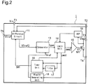
- Fig. 2 is a block diagram showing an internal structure of the power supply control IC1.
- the power supply control IC1 includes a difference circuit 11, a comparator 13, a logic unit 14, a driver 15, a timer unit 16, a filter 17, a ripple generating unit 18, an overcurrent protection unit (OCP unit) 19, and a switching element M1, and these structural elements are integrated in a single chip.
- OCP unit overcurrent protection unit
- a drain of the switching element M1 constituted of an N-channel metal-oxide-semiconductor field-effect transistor (MOSFET) is connected to one terminal of the primary winding L1 via the switching output terminal T3.
- a source of the switching element M1 is connected to the application terminal of the ground potential via the ground terminal T4.
- VOR Np / Ns ⁇ Vout + Vf
- Np the number of turns of the primary winding L1
- Ns the number of turns of the secondary winding L2
- Vf forward voltage of the diode D2.
- a switching voltage Vsw as a drain voltage of the switching element M1 is expressed by the following equation (2).
- Vsw Vin + VOR
- the difference circuit 11 is connected to the power supply terminal T1 applied with the input voltage Vin, the feedback terminal T2 connected to the other terminal of the resistor R11 having one terminal applied with the switching voltage Vsw, and the REF terminal T5 connected to the one terminal of the resistor R12. In this way, the difference circuit 11 converts a difference between the switching voltage Vsw and the input voltage Vin into current with the resistor R11, and a REF terminal voltage VTref is generated at the REF terminal T5 by the current after the conversion and the resistor R12. In other words, the REF terminal voltage VTref is generated as a feedback signal of the flyback voltage VOR.
- the difference circuit 11 corresponds to a feedback signal output unit.
- the difference circuit 11 performs an operation of outputting the REF terminal voltage VTref as it is as an output VTref2 when a switching element M11 is in OFF state, and an operation of holding the output VTref2 at a certain timing.
- the difference circuit 11 outputs the output VTref2 to the comparator 13.
- the comparator 13 compares the output VTref2 with a reference voltage Vref having a triangular wave, for example, generated by the ripple generating unit 18, and outputs a result of the comparison as an FET on trigger signal Tgon to the logic unit 14.
- the comparator 13 corresponds to an on trigger signal generating unit.
- the logic unit 14 generates a first PWM signal pwm1 and a second PWM signal pwm2.
- the first PWM signal pwm1 and the second PWM signal pwm2 are pulse-like signals having basically the same on duty.
- the filter 17 filters the first PWM signal pwm1 so as to extract on duty information.
- the filter 17 corresponds to a duty information obtaining unit.
- the timer unit 16 and the logic unit 14 set an ON time, which is a period during which the switching element M1 is in ON state, on the basis of the on duty information from the filter 17.
- the logic unit 14 sets the second PWM signal pwm2 to Low level so as to switch the switching element M1 from ON to OFF state at timing when the set ON time comes.
- the timer unit 16 and the logic unit 14 set a minimum OFF time as a minimum value of an OFF time, which is a period during which the switching element M1 is in OFF state, on the basis of the on duty information from the filter 17.
- the logic unit 14 sets the second PWM signal pwm2 to High level to switch the switching element M1 from OFF to ON state at timing based on the set minimum OFF time and the FET on trigger signal Tgon from the comparator 13.
- the driver 15 generates a gate voltage GT on the basis of the second PWM signal pwm2 generated by the logic unit 14 and applies the gate voltage GT to the gate of the switching element M1. In this way, the switching element M1 is on/off controlled.
- the timer unit 16 generates a switch timing signal SWT that instructs on/off timing of a switch (not shown) included in the difference circuit 11 and outputs the switch timing signal SWT to the difference circuit 11.
- the switch timing signal SWT instructs to turn on
- the difference circuit 11 outputs the REF terminal voltage VTref as it is as the output VTref2.
- the switch timing signal SWT instructs to turn off
- the difference circuit 11 holds the output VTref2 at switching timing from ON to OFF state.
- FIG. 3 is a diagram showing a specific structural example of the timer unit 16 and the logic unit 14.
- the timer unit 16 includes a minimum OFF time timer 161, a 1/2 ON time timer 162, a minimum ON time timer 163, an ON time timer 164, and an inverter 165.
- the logic unit 14 includes a first latch circuit 141, a second latch circuit 142, AND circuits 143 to 145, and an OR circuit 146.
- the first latch circuit 141 outputs the first PWM signal pwm1.
- the second latch circuit 142 outputs the second PWM signal pwm2 to the driver 15.
- the first latch circuit 141 and the second latch circuit 142 are simultaneously set by a signal input to a set terminal, and are basically simultaneously reset (except when the OCP unit 19 detects overcurrent) by a signal input to a reset terminal. Therefore, the first PWM signal pwm1 and the second PWM signal pwm2 are synchronized and have the same on duty.
- the minimum ON time timer 163 After being reset, the minimum ON time timer 163 starts to measure a predetermined minimum ON time (fixed value).
- the predetermined minimum ON time is a parameter that determines amount of overboost of the output voltage Vout.
- the ON time timer 164 After being reset, the ON time timer 164 starts to measure an ON time set by a filter output voltage V1 generated by the filter 17 on the basis of the first PWM signal pwm1.
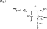
- Fig. 4 is a diagram showing a structural example of the filter 17.
- the filter 17 includes a resistor R17, a capacitor C17, and resistors R171 and R172 for voltage division.
- One terminal of the resistor R17 is connected to an input terminal T171 to which the first PWM signal pwm1 is applied.
- the other terminal of the resistor R17 is connected to one terminal of the capacitor C17 and is connected to a first output terminal T 172 at which the filter output voltage V1 is generated.
- the other terminal of the capacitor C17 is connected to the application terminal of the ground potential.
- the resistor R17 and the capacitor C17 constitute a low pass filter, and the first PWM signal pwm1 passes through the low pass filter to be the filter output voltage V1. Therefore, the filter output voltage V1 indicates the on duty information of the first PWM signal pwm1.
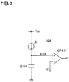
- Fig. 5 is a diagram showing a structural example of the ON time timer 164.
- the ON time timer 164 is a so-called ramp counter including a constant current circuit Ic, a capacitor C164, and a comparator CP164.
- the constant current circuit Ic and the capacitor C164 are connected in series between a power supply voltage Vcc and the ground potential, and the connection node between them is connected to a noninverting input terminal (+) of the comparator CP164.
- An inverting input terminal (-) of the comparator CP164 is applied with the filter output voltage V1.
- the output of the comparator CP164 is the output of the ON time timer 164.
- the output of the comparator CP164 is at Low level when it is reset, but after the time t described above elapses and the voltage V164 at the noninverting input terminal of the comparator CP164 reaches the filter output voltage V1, the output of the comparator CP164 becomes High level.
- the minimum ON time timer 163 can be constituted of a ramp counter having the same structure as illustrated in Fig. 5 .
- the reference voltage of the comparator, the constant current value of the constant current circuit, and the capacitance of the capacitor are appropriately set so that the time t described above will be the predetermined minimum ON time.
- the output of the minimum ON time timer 163 and the output of the ON time timer 164 are input to the AND circuit 145.
- the output of the AND circuit 145 becomes High level when both outputs of the minimum ON time timer 163 and the ON time timer 165 become High level.
- the output of the AND circuit 145 becomes High level at the timing when one of the predetermined minimum ON time measured by the minimum ON time timer 163 and the ON time measured by the ON time timer 164, which is longer, is measured. Therefore, if the ON time is shorter than the predetermined minimum ON time, the predetermined minimum ON time is dominant.
- the AND circuit 145 corresponds to an off timing determining unit.
- the output of the AND circuit 145 is input to a reset terminal of the first latch circuit 141 and is input to the OR circuit 146.
- the OR circuit 146 is also supplied with an output of the OCP unit 19.
- An output of the OR circuit 146 is input to the second latch circuit 142.
- the output of the OCP unit 19 is Low level in a normal time where overcurrent is not detected, and hence both the first latch circuit 141 and the second latch circuit 142 are reset at timing when the output of the AND circuit 145 becomes High level.
- the OR circuit 146 and the second latch circuit 142 constitute an off control unit.
- both the first PWM signal pwm1 and the second PWM signal pwm2 are switched to Low level, and the second PWM signal pwm2 turns off the switching element M1 so as to define the ON time.
- both the minimum OFF time timer 161 and the 1/2 ON time timer 162 are reset. After being reset, the minimum OFF time timer 161 starts to measure a predetermined minimum OFF time (fixed value).
- the difference circuit 11 outputs the REF terminal voltage VTref as it is or holds the output. Because ringing occurs in the switching voltage Vsw just after the switching element M1 is turned off, it is necessary to secure time until the ringing is stabilized, and therefore the predetermined minimum OFF time described above is determined.
- the minimum OFF time timer can be constituted of a ramp counter having the same structure as illustrated in Fig. 5 .
- the reference voltage of the comparator, the constant current value of the constant current circuit, and the capacitance of the capacitor are appropriately set so that the time t described above will be the predetermined minimum OFF time.
- the 1/2 ON time timer 162 starts to measure time that is 50% of the ON time.
- primary side current Ip flowing in the primary winding L1 increases.
- secondary side current Is flowing in the secondary winding L2 has a peak value that is obtained by multiplying the peak value of the primary side current by the turns ratio. Further, the secondary side current is gradually decreased as time elapses.
- Fig. 6 is a diagram of an example showing a manner in which the secondary side current Is is decreased when the switching element M1 is turned off. As shown in Fig.
- the secondary side current Is is gradually decreased from peak value Ispk when the switching element M1 is turned off and becomes zero when a discharge time toff2 elapses.
- the efficiency is lowered.
- the discharge time (i.e. the OFF time) can be elongated to 50% of the discharge time toff2.
- the actual discharge time toff2 depends on the transformer Tr1 and a load condition, it is difficult to estimate it. Therefore, in this embodiment, as an index similar to 50% of the discharge time toff2, the OFF time is elongated to 50% of the ON time.
- the filter output voltage V1 is divided by the resistors R171 and R172 having the same resistance so as to output the divided voltage as a filter output voltage V2 from a second output terminal T173.
- the filter output voltage V2 becomes 50% of the filter output voltage V1.
- the 1/2 ON time timer 162 is constituted to have the same structure as the ramp counter illustrated in Fig. 5 , and the filter output voltage V2 is applied as the reference voltage of the comparator. In this way, the 1/2 ON time timer 162 outputs High level when 50% of the ON time is measured after the output becomes Low level after being reset.
- the AND circuit 144 is supplied with outputs of the minimum OFF time timer 161 and the 1/2 ON time timer 162. An output of the AND circuit 144 becomes High level when both outputs of the minimum OFF time timer 161 and the 1/2 ON time timer 162 become High level. In other words, one of the predetermined minimum OFF time and 50% of the ON time, which is longer, is selected and set as the minimum OFF time.
- the AND circuit 144 corresponds to a minimum OFF time setting unit.
- the AND circuit 143 is supplied with the FET on trigger signal Tgon and the output of the AND circuit 144. In this way, when both the FET on trigger signal Tgon and the output of the AND circuit 144 become High level, the output of the AND circuit 143 becomes High level. In other words, if the timing when the FET on trigger signal Tgon becomes High level is after the minimum OFF time set as described above elapses, the timing is selected. If the timing when the minimum OFF time set as described above elapses is after the timing when the FET on trigger signal Tgon becomes High level, the timing when the minimum OFF time elapses is selected. In other words, the OFF time is limited so as not to be shorter than the minimum OFF time.
- the AND circuit 143 corresponds to an on timing determining unit.
- the output of the AND circuit 143 is input to the set terminals of the first latch circuit 141 and the second latch circuit 142. Therefore, at the timing when the output of the AND circuit 143 becomes High level, the first latch circuit 141 and the second latch circuit 142 are both set, and both the first PWM signal pwm1 and the second PWM signal pwm2 are switched to High level. In this way, the switching element M1 is turned on so as to define the OFF time.
- the switching element M1 When the output voltage Vout is decreased by a load fluctuation, the switching element M1 is turned on so as to determine the minimum OFF time set as described above as the OFF time. In this case, the on duty of the first PWM signal pwm1 is increased, and the ON time set by the filter output voltage V1 is elongated. In this way, by performing adaptive ON time control in which on duty information of the first PWM signal pwm1 is used to set the ON time, response characteristics to the load fluctuation can be improved.
- Fig. 7 is a timing chart showing an example of PWM signals and timer outputs of a transient response when the output voltage Vout is decreased by the load fluctuation.
- Fig. 7 also shows other signals including the voltage V164 at the noninverting input terminal of the comparator CP164 in the ON time timer 164 ( Fig. 5 ), the outputs of the AND circuits 145 and 144, and the FET on trigger signal Tgon.
- both the first PWM signal pwm1 and the second PWM signal pwm2 become High level, and the switching element M1 is turned on.
- both the minimum ON time timer 163 and the ON time timer 164 are reset, and the outputs of the timers become Low level.
- the ON time timer 164 is reset, the capacitor C164 is discharged, and hence the voltage V164 becomes zero.
- the constant current circuit Ic charges the capacitor C164, and hence the voltage V164 is increased at a predetermined speed.
- the minimum ON time timer 163 measures the predetermined minimum ON time
- the output of the minimum ON time timer 163 becomes High level (at timing t2).
- the output of the ON time timer 164 becomes High level (at timing t3).
- the output of the AND circuit 145 becomes High level, and hence the first latch circuit 141 and the second latch circuit 142 are both reset.
- both the first PWM signal pwm1 and the second PWM signal pwm2 become Low level, and the switching element M1 is turned off.
- the minimum OFF time timer 161 and the 1/2 ON time timer 162 are both reset, and the outputs of the timers become Low level.
- the minimum OFF time timer 161 measures the predetermined minimum OFF time, and hence an output of the minimum OFF time timer 161 becomes High level (at timing t4).
- the 1/2 ON time timer 162 measures the time that is 50% of the ON time, the output of the 1/2 ON time timer 162 becomes High level (at timing t5).
- the FET on trigger signal Tgon becomes High level at timing before the timing t5
- the output of the AND circuit 143 becomes High level at the timing t5.
- the first latch circuit 141 and the second latch circuit 142 are both set, and both the first PWM signal pwm1 and the second PWM signal pwm2 become High level.
- the switching element M1 is turned on.
- the ON time timer 164 determines the ON time. In other words, the ON time timer 164 as an ON time setting unit determines the ON time based on a switching duty of the switching element M1. Further, the 1/2 ON time timer 162 measures the time that is 50% of the ON time set by the ON time timer 164.
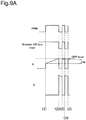
- Fig. 8A is a timing chart showing an example of waveforms in the embodiment for comparison in which only the minimum OFF time timer is used.
- Fig. 8A shows an example of waveforms of the PWM signal, the output of the minimum OFF time timer, the primary side current Ip, and the secondary side current Is, from top to bottom.
- Fig. 8A shows a case where the output voltage Vout is decreased by the load fluctuation after timing t11 when the PWM signal becomes High level and the switching element is turned on.
- the primary side current Ip is increased.
- the minimum OFF time timer is reset, and then the measurement of the predetermined minimum OFF time is started.
- the primary side current Ip becomes zero, and the secondary side current Is is generated in accordance with the peak value of the primary side current Ip and is decreased after that.
- the measurement of the minimum OFF time is completed at timing t13, and the output of the minimum OFF time timer becomes High level.
- the FET on trigger signal Tgon has become High level before the timing t13 due to the decrease of the output voltage Vout
- the PWM signal becomes High level at the timing t13, and the switching element is turned on.
- the secondary side current Is becomes zero
- the primary side current Ip is generated in accordance with a value of the secondary side current Is and then increases.
- the PWM signal becomes Low level at timing t14, and the switching element is turned off. In this case, the primary side current Ip becomes zero.
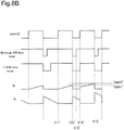
- Fig. 8B is a timing chart of this embodiment corresponding to Fig. 8A of the comparative example.
- Fig. 8B shows an example of waveforms of the first PWM signal pwm1 (and the second PWM signal pwm2), the output of the minimum OFF time timer 161, the output of the 1/2 ON time timer 162, the primary side current Ip, and the secondary side current Is, from top to bottom.
- both the minimum OFF time timer 161 and the 1/2 ON time timer 162 are reset, and each timer starts to measure time.
- the primary side current Ip becomes zero, and the secondary side current Is occurs and then decreases.
- the 1/2 ON time timer 162 completes measurement of 50% of the ON time at timing t14' after timing t13' when the minimum OFF time timer 161 completes measurement of the predetermined minimum OFF time.
- the FET on trigger signal Tgon has become High level before the timing t14' due to the decrease of the output voltage Vout
- the first PWM signal pwm1 becomes High level at the timing t14', and the switching element M1 is turned on.
- the secondary side current Is becomes zero
- the primary side current Ip is generated in accordance with a value of the secondary side current Is and then increases.
- the first PWM signal pwm1 becomes Low level at timing t15', and the switching element M1 is turned off. In this case, the primary side current Ip becomes zero.
- Fig. 8B compared with Fig. 8A , because the OFF time is defined at the timing when 50% of the ON time, which is longer than the predetermined minimum OFF time, is measured, the secondary side current Is is decreased down to a lower value by securing discharge time on the secondary side. In this way, the primary side current Ip generated when the switching element M1 is turned on can be decreased. Therefore, compared with an increase variation amount from a peak value Ippk1 to a peak value Ippk2 of the primary side current in Fig. 8A , an increase variation amount from a peak value Ippk1' to a peak value Ippk2' of the primary side current in Fig. 8B can reduced.
- a fluctuation in a switching period can be smaller in Fig. 8B than in Fig. 8A .
- the time to be compared with the predetermined minimum OFF time is not limited to a fixed predetermined ratio (e.g. 50%) of the ON time, but the predetermined ratio may be controlled in a variable manner in accordance with a load condition.
- Fig. 9A is a timing chart showing an example of an operation of the isolation type switching power supply device according to a comparative example in the overcurrent protection for comparing with this embodiment.
- the primary side current Ip starts to flow and then increases at timing t21 when the PWM signal becomes High level and the switching element is turned on. Further, the PWM signal becomes Low level at timing t22 when overcurrent occurs in the primary side current Ip and it is detected that the primary side current Ip has reached a predetermined OCP level, and the switching element is turned off. In this case, the primary side current Ip becomes zero, and the secondary side current Is occurs and then decreases.
- the minimum OFF time timer is reset at timing t22, and starts to measure the predetermined minimum OFF time. Further, when measurement of the minimum OFF time is completed at timing t23, the PWM signal becomes High level, and the switching element is turned on. In this case, the secondary side current Is becomes zero, and the primary side current Ip starts to flow and then increases. Further, the PWM signal becomes Low level at timing t24 when it is detected that the primary side current Ip has reached the OCP level, and the switching element is turned off. In this case, the primary side current Ip becomes zero, and the secondary side current Is starts to flow.
- a timing chart of an example of an operation of this embodiment in the overcurrent protection is shown in Fig. 9B .
- the OCP unit 19 detects overcurrent by detecting that the switching voltage Vsw obtained by multiplying a current value of the primary side current Ip by an on-resistance of the switching element M1 has reached a predetermined reference voltage.
- the primary side current Ip starts to flow and then increases. Further, when the OCP unit 19 detects overcurrent of the primary side current Ip at timing t22', the OCP unit 19 outputs the output signal of High level to the OR circuit 146 ( Fig. 3 ). In this way, the output of the OR circuit 146 becomes High level, the second latch circuit 142 is reset, the second PWM signal pwm2 becomes Low level, and the switching element M1 is turned off. In this case, the primary side current Ip becomes zero, and the secondary side current Is stars to flow and then decreases.
- the output of the AND circuit 145 is Low level at the timing t22', and the second PWM signal pwm2 becomes Low level because the primary side current Ip has reached the OCP level.
- the first latch circuit 141 is not reset, and the first PWM signal pwm1 holds High level.
- the first latch circuit 141 is reset, and the first PWM signal pwm1 becomes Low level.
- the minimum OFF time timer 161 and the 1/2 ON time timer 162 are both reset and start to measure time.
- the 1/2 ON time timer 162 completes measurement of the 50% of the ON time at timing t25'.
- the first latch circuit 141 and the second latch circuit 142 are both set at timing 25', and both the first PWM signal pwm1 and the second PWM signal pwm2 become High level. In this way, the switching element M1 is turned on. In this case, the secondary side current Is becomes zero, and the primary side current Ip starts to flow and then increase.
- the second PWM signal pwm2 becomes Low level, and the switching element M1 is turned off. In this case, the primary side current Ip becomes zero, and the secondary side current Is starts to flow and then decreases.
- the switching element M1 is turned off at the timing t22' when the overcurrent is detected, but at the timing t23' after that, the first PWM signal pwm1 becomes Low level, and the minimum OFF time timer 161 and the 1/2 ON time timer 162 are reset. Therefore, the discharge time on the secondary side is elongated by period T1 between the timing t22' and the timing t23'. Further, in this embodiment, the 1/2 ON time timer 162 measures period T2 longer than the predetermined minimum OFF time so as to define the OFF time, and hence the discharge time is elongated more.
- an increase variation amount ⁇ Ip' that is a value when the primary side current Ip starts to flow as illustrated in Fig. 9B according to this embodiment can be smaller than an increase variation amount ⁇ Ip that is a value when the primary side current Ip starts to flow as illustrated in Fig. 9A according to the comparative example.
- Fig. 9A because the increase variation amount ⁇ Ip becomes large and the primary side current Ip soon reaches the OCP level (at the timing t24), charge time on the primary side is shortened and the output voltage increases slowly.
- the increase variation amount ⁇ Ip becomes large and the primary side current Ip soon reaches the OCP level (at the timing t24)
- the difference circuit 11 outputs the REF terminal voltage VTref as it is or holds the output when the switching element M1 is in OFF state.
- a structure for controlling the output timing of the difference circuit 11 is illustrated in Fig. 10 .
- the timer unit 16 illustrated in Fig. 10 corresponds to a timing control unit.
- the timer unit 16 illustrated in Fig. 10 includes a minimum OFF time timer 1611, a 1/2 ON time timer 1621, an inverter 166, an AND circuit 167, a mask period timer 168, and a latch circuit 169. Note that the timer unit 16 illustrated in Fig. 10 is the same as the timer unit 16 illustrated in Fig. 3 described above. In other words, although the structure illustrated in Fig. 10 is not shown in the timer unit 16 illustrated in Fig. 3 , the structure is actually included in the timer unit 16.
- the minimum OFF time timer 1611 measures time that is 95% of the predetermined minimum OFF time measured by the minimum OFF time timer 161.
- the 1/2 ON time timer 1621 is constituted in the same manner as the ramp counter illustrated in Fig. 5 , and an output voltage V3 output from the filter 17 is applied as the reference voltage to the comparator.
- the output voltage V3 is a voltage that is 95% of the output voltage V2 described above ( Fig. 4 ).
- the 1/2 ON time timer 1621 measures time that is 95% of 50% of the ON time.
- the ratio of 95% for the minimum OFF time timer 1611 and the 1/2 ON time timer 1621 is merely an example, and other ratio may be used as long as it is less than 100% (e.g. a ratio of 70% or larger).
- the inverter 166 is supplied with the first PWM signal pwm1 output from the first latch circuit 141. Outputs of the minimum OFF time timer 1611, the 1/2 ON time timer 1621, and the inverter 166 are input to the AND circuit 167. An output of the AND circuit 167 is input to the reset terminal of the latch circuit 169.
- the mask period timer 168 measures a predetermined mask period (e.g. 240 nsec).
- the output of the mask period timer 168 is input to the set terminal of the latch circuit 169.
- the output of the latch circuit 169 is input to the difference circuit 11 as the switch timing signal SWT.
- the mask period timer 168 measures the predetermined mask period, its output becomes High level. Then, the latch circuit 169 is set, and the switch timing signal SWT becomes High level. In this way, a switch (not shown) included in the difference circuit 11 is turned on, and the difference circuit 11 starts operation to output the REF terminal voltage VTref as it is as the output VTref2.
- the AND circuit 167 becomes High level at one of the timing when the minimum OFF time timer 1611 has measured 95% of the predetermined minimum OFF time and the timing when the 1/2 ON time timer 1621 has measured 95% of 50% of the ON time, which is later. Then, the latch circuit 169 is reset, and the switch timing signal SWT becomes Low level. In this way, the switch included in the difference circuit 11 is turned off, and the difference circuit 11 holds the output VTref2 at switching timing from ON to OFF state.
- a waveform example of the switching voltage Vsw when the switching element M1 is turned off is shown in Fig. 11 .
- ringing occurs in the switching voltage Vsw due to leakage inductance of the primary winding L1 of the transformer Tr1. Accordingly, masking is performed for a mask period Tmsk using the mask period timer 168, so as not to perform the operation of outputting the REF terminal voltage VTref as it is for the period during which ringing occurs.
- the timing when the output is held is before the timing when the switching element M1 is turned on, the output can be held while the secondary side current Is is flowing. In other words, it is possible to prevent occurrence of abnormality in the output due to coincidence between the timing when the switching element M1 is turned on and the timing when the output is held.
- the REF terminal voltage VTref is the feedback signal of the flyback voltage VOR
- the flyback voltage VOR is expressed by the equation (1) described above.
- a portion corresponding to the forward voltage Vf of the diode D2 is an error portion. Therefore, as the secondary side current Is becomes closer to zero, Vf becomes smaller, and the error becomes smaller. In other words, as time elapses more, the timing for holding the output becomes more appropriate. If T1/2on is longer than Tmin_off, the timing for holding the output can be later.
- FIG. 12 A structure of an isolation type switching power supply device 10' according to the variation is illustrated in Fig. 12 .
- the isolation type switching power supply device 10' illustrated in Fig. 12 includes a power supply control IC1'.
- the power supply control IC1' has a structure including the main switching element M11, a sub-switching element M12, the resistor R12, and a comparator CP. Note that in the power supply control IC1', structural portions other than those illustrated in Fig. 12 are similar to those of the embodiment described above ( Fig. 2 ).
- the main switching element M11 constituted of an N-channel MOSFET is a switching element that is switching-driven so as to contribute to generation of the output voltage Vout in the isolation type switching power supply device 10'.
- the drain (current input terminal) of the main switching element M11 is connected to the switching output terminal T3, and the source (current output terminal) of the same is connected to a ground terminal T41.
- the sub-switching element M12 is constituted of an N-channel MOSFET.
- the drain (current input terminal) of the sub-switching element M12 is connected to a connection node between the drain of the main switching element M11 and the switching output terminal T3 via the resistor R12.
- the source (current output terminal) of the sub-switching element M12 is connected to a ground terminal T42.
- the gate (control terminal) of the main switching element M11 is connected to an output terminal of a not-shown driver.
- the noninverting input terminal (+) of the comparator CP is connected to the gate of the switching element M11.
- the inverting input terminal (-) of the comparator CP is applied with a predetermined threshold value voltage Vth1 as the reference voltage.
- the output terminal of the comparator CP is connected to the gate (control terminal) of the sub-switching element M12.
- the comparator CP corresponds to a voltage applying unit.
- Fig. 13 is a timing chart showing an example of waveforms when the main switching element M11 is turned off.
- Fig. 13 shows a gate voltage Vg11 of the main switching element M11, a gate voltage Vg12 of the sub-switching element M12, a current (drain current) I11 flowing in the main switching element M11, the secondary side current Is, the switching voltage Vsw, and a current (drain current) I12 flowing in the sub-switching element M12, from top to bottom.
- the main switching element M11 When the main switching element M11 is in ON state (the sub-switching element M12 is in OFF state), drawing charge from a gate capacitor of the main switching element M11 is started at timing t31, in order to turn off the main switching element M11 with a not-shown driver. Then, the gate voltage Vg11 of the main switching element M11 is decreased. Further, after the gate voltage Vg11 reaches a mirror voltage Vm, at timing t32 when the gate voltage Vg11 decreases from the mirror voltage Vm, the current I11 starts to decrease, and the switching voltage Vsw starts to increase. Further, when the gate voltage Vg11 reaches the threshold value voltage Vth1, the output of the comparator CP becomes Low level (at timing t33).
- the primary winding L1 of the transformer Tr1 has a leakage inductance, and current flows also in the leakage inductance so as to store energy when the switching element is in ON state, but without any coupling with other windings, power transition is not performed. In this way, if the sub-switching element M12 is not disposed, large ringing occurs for long period in the switching voltage Vsw when the main switching element M11 is turned off.
- ringing that may occur in the switching voltage Vsw can be reduced by allowing the current I12 to flow in the sub-switching element M12 when the main switching element M11 is turned off.
- Fig. 13 shows that a peak value of the ringing generated in the switching voltage Vsw without the sub-switching element M12 (a broken line) can be reduced to a peak value of the switching voltage Vsw in this embodiment shown by a solid line.
- a Snubber circuit may be used in order to reduce the ringing, but a Snubber circuit is difficult to design for a user. If the design is failed, the switching element may be broken. According to this embodiment, the ringing can be reduced without using such a Snubber circuit.
- the threshold value voltage Vth1 of the comparator CP is set to a value between the mirror voltage Vm of the main switching element M11 and the threshold value voltage Vth11 of the main switching element M11 itself.
- the current I11 flowing in the main switching element M11 decreases after the gate voltage Vg11 is decreased from the mirror voltage Vm and becomes zero when the gate voltage Vg11 reaches the threshold value voltage Vth11. If the threshold value voltage Vth1 is set to the mirror voltage Vm or higher, almost no current flows in the sub-switching element M12 during the period in which the gate voltage Vg11 is the threshold value voltage Vth1 to the mirror voltage Vm, and hence the sub-switching element M12 does not function during the period.
- the threshold value voltage Vth1 is set to the threshold value voltage Vth11 or lower, the timing when the gate voltage Vg12 reaches the threshold value voltage Vth12 is delayed, and the current I12 flows excessively in the sub-switching element M12. Therefore, it is preferred to set the threshold value voltage Vth1 to a value lower than the mirror voltage Vm, and it is more preferred to set the same to a value between the mirror voltage Vm and the threshold value voltage Vth11.
- the resistor R12 is provided for limiting the current I12.
- the period (from the timing t32 to the timing t34) in which the sub-switching element M12 is turned on there is the period (from the timing t32 to the timing t34) in which the sub-switching element M12 is turned on. In this period, as the current flowing from the switching output terminal T3 to the ground terminals T41 and T42, the current flows in the main switching element M11 having low resistance, and almost no current flows in the sub-switching element M12 because of the resistor R12. If the current I12 is allowed to flow excessively, rising voltage of the switching voltage Vsw becomes abnormally low when the main switching element M11 is turned off.
- the main switching element M11 and the sub-switching element M12 be manufactured by the same process, and the main switching element M11 has a larger size than the sub-switching element M12 (e.g. 1000:1).
- the main switching element M11 and the sub-switching element M12 have the same variation and the same characteristics. Therefore, the time after the gate voltage starts to decrease until it becomes zero (or until it reaches the threshold value voltage of the switching element) is substantially the same between the main switching element M11 and the sub-switching element M12. Therefore, when the current I11 of the main switching element M11 becomes zero, it is secured that the sub-switching element M12 is in ON state.
- a delay circuit such as a filter that delays the voltage to be applied to the gate of the main switching element M11 and applies the delayed voltage to the gate of the sub-switching element M12. For example, the delay time elapses before the current I11 of the main switching element M11 becomes zero, and the sub-switching element M12 keeps its ON state when the current of the main switching element M11 is zero. Thus, ringing can be reduced.
- the switching element may be disposed externally of the power supply control IC instead of being included in the same.
- isolation type switching power supply device may be appropriately used for an industrial inverter such as a solar inverter, an FA inverter, or a power storage system.
Landscapes
- Engineering & Computer Science (AREA)
- Power Engineering (AREA)
- Dc-Dc Converters (AREA)
Applications Claiming Priority (5)
| Application Number | Priority Date | Filing Date | Title |
|---|---|---|---|
| JP2016181320A JP6730892B2 (ja) | 2016-09-16 | 2016-09-16 | 電源制御装置、および絶縁型スイッチング電源装置 |
| JP2016181322A JP6730893B2 (ja) | 2016-09-16 | 2016-09-16 | 電源制御装置、および絶縁型スイッチング電源装置 |
| JP2016181323 | 2016-09-16 | ||
| JP2016181325A JP6775365B2 (ja) | 2016-09-16 | 2016-09-16 | 絶縁型スイッチング電源装置、および電源制御装置 |
| JP2016235245A JP6806548B2 (ja) | 2016-09-16 | 2016-12-02 | 電源制御装置、および絶縁型スイッチング電源装置 |
Publications (2)
| Publication Number | Publication Date |
|---|---|
| EP3301802A1 true EP3301802A1 (fr) | 2018-04-04 |
| EP3301802B1 EP3301802B1 (fr) | 2019-04-24 |
Family
ID=59887143
Family Applications (1)
| Application Number | Title | Priority Date | Filing Date |
|---|---|---|---|
| EP17191372.6A Not-in-force EP3301802B1 (fr) | 2016-09-16 | 2017-09-15 | Unité de commande d'alimentation électrique et dispositif d'alimentation électrique de commutation de type à isolation |
Country Status (3)
| Country | Link |
|---|---|
| US (1) | US10491127B2 (fr) |
| EP (1) | EP3301802B1 (fr) |
| CN (1) | CN107834857B (fr) |
Cited By (1)
| Publication number | Priority date | Publication date | Assignee | Title |
|---|---|---|---|---|
| US10759714B2 (en) | 2016-09-30 | 2020-09-01 | Infineon Technologies Ag | Method for producing a metal-ceramic substrate |
Families Citing this family (4)
| Publication number | Priority date | Publication date | Assignee | Title |
|---|---|---|---|---|
| WO2020202760A1 (fr) * | 2019-03-29 | 2020-10-08 | 富士電機株式会社 | Circuit de commande de commutation, circuit d'alimentation électrique |
| JP7498638B2 (ja) * | 2020-10-15 | 2024-06-12 | ローム株式会社 | 電源制御装置、絶縁型スイッチング電源 |
| US11387740B1 (en) * | 2021-06-23 | 2022-07-12 | Monolithic Power Systems, Inc. | Energy recycle circuit for flyback circuit and method thereof |
| US11973431B2 (en) * | 2022-04-07 | 2024-04-30 | Sanken Electric Co., Ltd. | Switching power supply apparatus |
Citations (5)
| Publication number | Priority date | Publication date | Assignee | Title |
|---|---|---|---|---|
| EP0827263A2 (fr) * | 1996-08-29 | 1998-03-04 | Trw Inc. | Convertisseur direct double avec commutation à largeur d'impulsions douce |
| US6445598B1 (en) * | 1999-12-09 | 2002-09-03 | Sanken Electric Co., Ltd. | Dc-dc converter |
| US20030038615A1 (en) * | 2001-08-23 | 2003-02-27 | Fairchild Semiconductor Corporation | Method and circuit for reducing losses in DC-DC converters |
| JP2012125084A (ja) | 2010-12-10 | 2012-06-28 | Mitsumi Electric Co Ltd | 絶縁型直流電源装置 |
| US20150318790A1 (en) * | 2014-04-30 | 2015-11-05 | Semiconductor Components Industries, Llc | Method and apparatus for synchronous rectifier operation |
Family Cites Families (7)
| Publication number | Priority date | Publication date | Assignee | Title |
|---|---|---|---|---|
| JP3028044B2 (ja) * | 1995-04-17 | 2000-04-04 | 松下電器産業株式会社 | スイッチング電源装置 |
| TW200740089A (en) * | 2006-03-07 | 2007-10-16 | Rohm Co Ltd | Capacitor charging apparatus |
| US8125798B2 (en) * | 2008-07-01 | 2012-02-28 | Active-Semi, Inc. | Constant current and voltage controller in a three-pin package operating in critical conduction mode |
| JP4803262B2 (ja) * | 2009-01-27 | 2011-10-26 | 株式会社村田製作所 | 絶縁型スイッチング電源装置 |
| CN102412727B (zh) * | 2011-11-25 | 2014-02-19 | 成都芯源系统有限公司 | 开关电源及其控制电路和调光方法 |
| TWI523395B (zh) | 2013-11-05 | 2016-02-21 | 通嘉科技股份有限公司 | 開關式電源供應器之時脈頻率控制方法以及相關之電源控制裝置 |
| TWI562525B (en) | 2014-08-15 | 2016-12-11 | Eosmem Corp | Primary-side regulated flyback converter and power control integrated circuit thereof |
-
2017
- 2017-09-14 US US15/704,256 patent/US10491127B2/en active Active
- 2017-09-15 EP EP17191372.6A patent/EP3301802B1/fr not_active Not-in-force
- 2017-09-15 CN CN201710833585.9A patent/CN107834857B/zh not_active Expired - Fee Related
Patent Citations (5)
| Publication number | Priority date | Publication date | Assignee | Title |
|---|---|---|---|---|
| EP0827263A2 (fr) * | 1996-08-29 | 1998-03-04 | Trw Inc. | Convertisseur direct double avec commutation à largeur d'impulsions douce |
| US6445598B1 (en) * | 1999-12-09 | 2002-09-03 | Sanken Electric Co., Ltd. | Dc-dc converter |
| US20030038615A1 (en) * | 2001-08-23 | 2003-02-27 | Fairchild Semiconductor Corporation | Method and circuit for reducing losses in DC-DC converters |
| JP2012125084A (ja) | 2010-12-10 | 2012-06-28 | Mitsumi Electric Co Ltd | 絶縁型直流電源装置 |
| US20150318790A1 (en) * | 2014-04-30 | 2015-11-05 | Semiconductor Components Industries, Llc | Method and apparatus for synchronous rectifier operation |
Cited By (1)
| Publication number | Priority date | Publication date | Assignee | Title |
|---|---|---|---|---|
| US10759714B2 (en) | 2016-09-30 | 2020-09-01 | Infineon Technologies Ag | Method for producing a metal-ceramic substrate |
Also Published As
| Publication number | Publication date |
|---|---|
| US10491127B2 (en) | 2019-11-26 |
| CN107834857B (zh) | 2020-02-28 |
| CN107834857A (zh) | 2018-03-23 |
| EP3301802B1 (fr) | 2019-04-24 |
| US20180083543A1 (en) | 2018-03-22 |
Similar Documents
| Publication | Publication Date | Title |
|---|---|---|
| CN112134453B (zh) | 启动控制方法及系统、尖峰电压检测电路及方法 | |
| US10924003B2 (en) | Switching power supply | |
| US8669748B2 (en) | Device for synchronous DC-DC conversion and synchronous DC-DC converter | |
| JP4173874B2 (ja) | 昇圧コンバータ | |
| CN102377336B (zh) | 开关电源装置 | |
| US9647562B2 (en) | Power conversion with switch turn-off delay time compensation | |
| US20250125738A1 (en) | Systems and methods for controlling synchronous rectifiers in power converters with zero voltage switching | |
| EP3301802B1 (fr) | Unité de commande d'alimentation électrique et dispositif d'alimentation électrique de commutation de type à isolation | |
| JP5418899B2 (ja) | 電力コンバータでの使用のための制御回路および電力コンバータにおける変圧器の飽和を防止する方法 | |
| US12362650B2 (en) | Switch-mode power converters with control of turning off transistors for zero-voltage switching | |
| US20130329468A1 (en) | Switching controller with clamp circuit for capacitor-less power supplies | |
| JP2003259641A (ja) | 直流電圧変換回路 | |
| JP6806548B2 (ja) | 電源制御装置、および絶縁型スイッチング電源装置 | |
| US10284087B2 (en) | Step-up/step-down DC-DC converter | |
| WO2022130910A1 (fr) | Dispositif de commande d'alimentation électrique et convertisseur indirect | |
| JP6730893B2 (ja) | 電源制御装置、および絶縁型スイッチング電源装置 | |
| CN112087148A (zh) | 一种同步整流控制电路及反激式开关电源 | |
| JP6775365B2 (ja) | 絶縁型スイッチング電源装置、および電源制御装置 | |
| JP7543296B2 (ja) | スイッチング制御回路及びスイッチング電源装置 | |
| JP6730892B2 (ja) | 電源制御装置、および絶縁型スイッチング電源装置 | |
| TWI677177B (zh) | 電源控制裝置、及絕緣型開關電源裝置 | |
| US10924020B1 (en) | Prestart control circuit for a switching power converter | |
| JP2024003305A (ja) | スイッチ駆動回路、電源制御装置、スイッチング電源 | |
| JP2004229428A (ja) | スイッチング電源装置 | |
| CN119341319A (zh) | 开关电源装置以及电源控制用半导体装置 |
Legal Events
| Date | Code | Title | Description |
|---|---|---|---|
| PUAI | Public reference made under article 153(3) epc to a published international application that has entered the european phase |
Free format text: ORIGINAL CODE: 0009012 |
|
| STAA | Information on the status of an ep patent application or granted ep patent |
Free format text: STATUS: REQUEST FOR EXAMINATION WAS MADE |
|
| 17P | Request for examination filed |
Effective date: 20170915 |
|
| AK | Designated contracting states |
Kind code of ref document: A1 Designated state(s): AL AT BE BG CH CY CZ DE DK EE ES FI FR GB GR HR HU IE IS IT LI LT LU LV MC MK MT NL NO PL PT RO RS SE SI SK SM TR |
|
| AX | Request for extension of the european patent |
Extension state: BA ME |
|
| RBV | Designated contracting states (corrected) |
Designated state(s): AL AT BE BG CH CY CZ DE DK EE ES FI FR GB GR HR HU IE IS IT LI LT LU LV MC MK MT NL NO PL PT RO RS SE SI SK SM TR |
|
| GRAP | Despatch of communication of intention to grant a patent |
Free format text: ORIGINAL CODE: EPIDOSNIGR1 |
|
| STAA | Information on the status of an ep patent application or granted ep patent |
Free format text: STATUS: GRANT OF PATENT IS INTENDED |
|
| INTG | Intention to grant announced |
Effective date: 20181116 |
|
| GRAS | Grant fee paid |
Free format text: ORIGINAL CODE: EPIDOSNIGR3 |
|
| GRAA | (expected) grant |
Free format text: ORIGINAL CODE: 0009210 |
|
| STAA | Information on the status of an ep patent application or granted ep patent |
Free format text: STATUS: THE PATENT HAS BEEN GRANTED |
|
| AK | Designated contracting states |
Kind code of ref document: B1 Designated state(s): AL AT BE BG CH CY CZ DE DK EE ES FI FR GB GR HR HU IE IS IT LI LT LU LV MC MK MT NL NO PL PT RO RS SE SI SK SM TR |
|
| REG | Reference to a national code |
Ref country code: GB Ref legal event code: FG4D |
|
| REG | Reference to a national code |
Ref country code: CH Ref legal event code: EP |
|
| REG | Reference to a national code |
Ref country code: AT Ref legal event code: REF Ref document number: 1125311 Country of ref document: AT Kind code of ref document: T Effective date: 20190515 Ref country code: IE Ref legal event code: FG4D |
|
| REG | Reference to a national code |
Ref country code: DE Ref legal event code: R096 Ref document number: 602017003485 Country of ref document: DE |
|
| REG | Reference to a national code |
Ref country code: NL Ref legal event code: MP Effective date: 20190424 |
|
| REG | Reference to a national code |
Ref country code: LT Ref legal event code: MG4D |
|
| PG25 | Lapsed in a contracting state [announced via postgrant information from national office to epo] |
Ref country code: NL Free format text: LAPSE BECAUSE OF FAILURE TO SUBMIT A TRANSLATION OF THE DESCRIPTION OR TO PAY THE FEE WITHIN THE PRESCRIBED TIME-LIMIT Effective date: 20190424 |
|
| PG25 | Lapsed in a contracting state [announced via postgrant information from national office to epo] |
Ref country code: NO Free format text: LAPSE BECAUSE OF FAILURE TO SUBMIT A TRANSLATION OF THE DESCRIPTION OR TO PAY THE FEE WITHIN THE PRESCRIBED TIME-LIMIT Effective date: 20190724 Ref country code: FI Free format text: LAPSE BECAUSE OF FAILURE TO SUBMIT A TRANSLATION OF THE DESCRIPTION OR TO PAY THE FEE WITHIN THE PRESCRIBED TIME-LIMIT Effective date: 20190424 Ref country code: LT Free format text: LAPSE BECAUSE OF FAILURE TO SUBMIT A TRANSLATION OF THE DESCRIPTION OR TO PAY THE FEE WITHIN THE PRESCRIBED TIME-LIMIT Effective date: 20190424 Ref country code: HR Free format text: LAPSE BECAUSE OF FAILURE TO SUBMIT A TRANSLATION OF THE DESCRIPTION OR TO PAY THE FEE WITHIN THE PRESCRIBED TIME-LIMIT Effective date: 20190424 Ref country code: SE Free format text: LAPSE BECAUSE OF FAILURE TO SUBMIT A TRANSLATION OF THE DESCRIPTION OR TO PAY THE FEE WITHIN THE PRESCRIBED TIME-LIMIT Effective date: 20190424 Ref country code: PT Free format text: LAPSE BECAUSE OF FAILURE TO SUBMIT A TRANSLATION OF THE DESCRIPTION OR TO PAY THE FEE WITHIN THE PRESCRIBED TIME-LIMIT Effective date: 20190824 Ref country code: AL Free format text: LAPSE BECAUSE OF FAILURE TO SUBMIT A TRANSLATION OF THE DESCRIPTION OR TO PAY THE FEE WITHIN THE PRESCRIBED TIME-LIMIT Effective date: 20190424 Ref country code: ES Free format text: LAPSE BECAUSE OF FAILURE TO SUBMIT A TRANSLATION OF THE DESCRIPTION OR TO PAY THE FEE WITHIN THE PRESCRIBED TIME-LIMIT Effective date: 20190424 |
|
| PG25 | Lapsed in a contracting state [announced via postgrant information from national office to epo] |
Ref country code: BG Free format text: LAPSE BECAUSE OF FAILURE TO SUBMIT A TRANSLATION OF THE DESCRIPTION OR TO PAY THE FEE WITHIN THE PRESCRIBED TIME-LIMIT Effective date: 20190724 Ref country code: RS Free format text: LAPSE BECAUSE OF FAILURE TO SUBMIT A TRANSLATION OF THE DESCRIPTION OR TO PAY THE FEE WITHIN THE PRESCRIBED TIME-LIMIT Effective date: 20190424 Ref country code: PL Free format text: LAPSE BECAUSE OF FAILURE TO SUBMIT A TRANSLATION OF THE DESCRIPTION OR TO PAY THE FEE WITHIN THE PRESCRIBED TIME-LIMIT Effective date: 20190424 Ref country code: LV Free format text: LAPSE BECAUSE OF FAILURE TO SUBMIT A TRANSLATION OF THE DESCRIPTION OR TO PAY THE FEE WITHIN THE PRESCRIBED TIME-LIMIT Effective date: 20190424 Ref country code: GR Free format text: LAPSE BECAUSE OF FAILURE TO SUBMIT A TRANSLATION OF THE DESCRIPTION OR TO PAY THE FEE WITHIN THE PRESCRIBED TIME-LIMIT Effective date: 20190725 |
|
| REG | Reference to a national code |
Ref country code: AT Ref legal event code: MK05 Ref document number: 1125311 Country of ref document: AT Kind code of ref document: T Effective date: 20190424 |
|
| PG25 | Lapsed in a contracting state [announced via postgrant information from national office to epo] |
Ref country code: IS Free format text: LAPSE BECAUSE OF FAILURE TO SUBMIT A TRANSLATION OF THE DESCRIPTION OR TO PAY THE FEE WITHIN THE PRESCRIBED TIME-LIMIT Effective date: 20190824 |
|
| REG | Reference to a national code |
Ref country code: DE Ref legal event code: R097 Ref document number: 602017003485 Country of ref document: DE |
|
| PG25 | Lapsed in a contracting state [announced via postgrant information from national office to epo] |
Ref country code: SK Free format text: LAPSE BECAUSE OF FAILURE TO SUBMIT A TRANSLATION OF THE DESCRIPTION OR TO PAY THE FEE WITHIN THE PRESCRIBED TIME-LIMIT Effective date: 20190424 Ref country code: EE Free format text: LAPSE BECAUSE OF FAILURE TO SUBMIT A TRANSLATION OF THE DESCRIPTION OR TO PAY THE FEE WITHIN THE PRESCRIBED TIME-LIMIT Effective date: 20190424 Ref country code: DK Free format text: LAPSE BECAUSE OF FAILURE TO SUBMIT A TRANSLATION OF THE DESCRIPTION OR TO PAY THE FEE WITHIN THE PRESCRIBED TIME-LIMIT Effective date: 20190424 Ref country code: AT Free format text: LAPSE BECAUSE OF FAILURE TO SUBMIT A TRANSLATION OF THE DESCRIPTION OR TO PAY THE FEE WITHIN THE PRESCRIBED TIME-LIMIT Effective date: 20190424 Ref country code: RO Free format text: LAPSE BECAUSE OF FAILURE TO SUBMIT A TRANSLATION OF THE DESCRIPTION OR TO PAY THE FEE WITHIN THE PRESCRIBED TIME-LIMIT Effective date: 20190424 Ref country code: CZ Free format text: LAPSE BECAUSE OF FAILURE TO SUBMIT A TRANSLATION OF THE DESCRIPTION OR TO PAY THE FEE WITHIN THE PRESCRIBED TIME-LIMIT Effective date: 20190424 |
|
| PG25 | Lapsed in a contracting state [announced via postgrant information from national office to epo] |
Ref country code: IT Free format text: LAPSE BECAUSE OF FAILURE TO SUBMIT A TRANSLATION OF THE DESCRIPTION OR TO PAY THE FEE WITHIN THE PRESCRIBED TIME-LIMIT Effective date: 20190424 Ref country code: SM Free format text: LAPSE BECAUSE OF FAILURE TO SUBMIT A TRANSLATION OF THE DESCRIPTION OR TO PAY THE FEE WITHIN THE PRESCRIBED TIME-LIMIT Effective date: 20190424 |
|
| PLBE | No opposition filed within time limit |
Free format text: ORIGINAL CODE: 0009261 |
|
| STAA | Information on the status of an ep patent application or granted ep patent |
Free format text: STATUS: NO OPPOSITION FILED WITHIN TIME LIMIT |
|
| PG25 | Lapsed in a contracting state [announced via postgrant information from national office to epo] |
Ref country code: TR Free format text: LAPSE BECAUSE OF FAILURE TO SUBMIT A TRANSLATION OF THE DESCRIPTION OR TO PAY THE FEE WITHIN THE PRESCRIBED TIME-LIMIT Effective date: 20190424 |
|
| 26N | No opposition filed |
Effective date: 20200127 |
|
| PG25 | Lapsed in a contracting state [announced via postgrant information from national office to epo] |
Ref country code: SI Free format text: LAPSE BECAUSE OF FAILURE TO SUBMIT A TRANSLATION OF THE DESCRIPTION OR TO PAY THE FEE WITHIN THE PRESCRIBED TIME-LIMIT Effective date: 20190424 Ref country code: MC Free format text: LAPSE BECAUSE OF FAILURE TO SUBMIT A TRANSLATION OF THE DESCRIPTION OR TO PAY THE FEE WITHIN THE PRESCRIBED TIME-LIMIT Effective date: 20190424 |
|
| PG25 | Lapsed in a contracting state [announced via postgrant information from national office to epo] |
Ref country code: LU Free format text: LAPSE BECAUSE OF NON-PAYMENT OF DUE FEES Effective date: 20190915 Ref country code: IE Free format text: LAPSE BECAUSE OF NON-PAYMENT OF DUE FEES Effective date: 20190915 |
|
| REG | Reference to a national code |
Ref country code: BE Ref legal event code: MM Effective date: 20190930 |
|
| PG25 | Lapsed in a contracting state [announced via postgrant information from national office to epo] |
Ref country code: BE Free format text: LAPSE BECAUSE OF NON-PAYMENT OF DUE FEES Effective date: 20190930 |
|
| PG25 | Lapsed in a contracting state [announced via postgrant information from national office to epo] |
Ref country code: FR Free format text: LAPSE BECAUSE OF NON-PAYMENT OF DUE FEES Effective date: 20190930 |
|
| REG | Reference to a national code |
Ref country code: CH Ref legal event code: PL |
|
| PG25 | Lapsed in a contracting state [announced via postgrant information from national office to epo] |
Ref country code: CY Free format text: LAPSE BECAUSE OF FAILURE TO SUBMIT A TRANSLATION OF THE DESCRIPTION OR TO PAY THE FEE WITHIN THE PRESCRIBED TIME-LIMIT Effective date: 20190424 |
|
| PG25 | Lapsed in a contracting state [announced via postgrant information from national office to epo] |
Ref country code: HU Free format text: LAPSE BECAUSE OF FAILURE TO SUBMIT A TRANSLATION OF THE DESCRIPTION OR TO PAY THE FEE WITHIN THE PRESCRIBED TIME-LIMIT; INVALID AB INITIO Effective date: 20170915 Ref country code: MT Free format text: LAPSE BECAUSE OF FAILURE TO SUBMIT A TRANSLATION OF THE DESCRIPTION OR TO PAY THE FEE WITHIN THE PRESCRIBED TIME-LIMIT Effective date: 20190424 |
|
| PG25 | Lapsed in a contracting state [announced via postgrant information from national office to epo] |
Ref country code: LI Free format text: LAPSE BECAUSE OF NON-PAYMENT OF DUE FEES Effective date: 20200930 Ref country code: CH Free format text: LAPSE BECAUSE OF NON-PAYMENT OF DUE FEES Effective date: 20200930 |
|
| PGFP | Annual fee paid to national office [announced via postgrant information from national office to epo] |
Ref country code: DE Payment date: 20210803 Year of fee payment: 5 |
|
| GBPC | Gb: european patent ceased through non-payment of renewal fee |
Effective date: 20210915 |
|
| PG25 | Lapsed in a contracting state [announced via postgrant information from national office to epo] |
Ref country code: MK Free format text: LAPSE BECAUSE OF FAILURE TO SUBMIT A TRANSLATION OF THE DESCRIPTION OR TO PAY THE FEE WITHIN THE PRESCRIBED TIME-LIMIT Effective date: 20190424 |
|
| PG25 | Lapsed in a contracting state [announced via postgrant information from national office to epo] |
Ref country code: GB Free format text: LAPSE BECAUSE OF NON-PAYMENT OF DUE FEES Effective date: 20210915 |
|
| REG | Reference to a national code |
Ref country code: DE Ref legal event code: R119 Ref document number: 602017003485 Country of ref document: DE |
|
| PG25 | Lapsed in a contracting state [announced via postgrant information from national office to epo] |
Ref country code: DE Free format text: LAPSE BECAUSE OF NON-PAYMENT OF DUE FEES Effective date: 20230401 |