EP3301810B1 - Circuits et procédés de filtre adaptatif - Google Patents
Circuits et procédés de filtre adaptatif Download PDFInfo
- Publication number
- EP3301810B1 EP3301810B1 EP16191469.2A EP16191469A EP3301810B1 EP 3301810 B1 EP3301810 B1 EP 3301810B1 EP 16191469 A EP16191469 A EP 16191469A EP 3301810 B1 EP3301810 B1 EP 3301810B1
- Authority
- EP
- European Patent Office
- Prior art keywords
- step size
- signal
- circuitry
- adaptive filter
- subject matter
- Prior art date
- Legal status (The legal status is an assumption and is not a legal conclusion. Google has not performed a legal analysis and makes no representation as to the accuracy of the status listed.)
- Active
Links
Images


Classifications
-
- H—ELECTRICITY
- H03—ELECTRONIC CIRCUITRY
- H03H—IMPEDANCE NETWORKS, e.g. RESONANT CIRCUITS; RESONATORS
- H03H21/00—Adaptive networks
- H03H21/0012—Digital adaptive filters
- H03H21/0043—Adaptive algorithms
-
- H—ELECTRICITY
- H03—ELECTRONIC CIRCUITRY
- H03H—IMPEDANCE NETWORKS, e.g. RESONANT CIRCUITS; RESONATORS
- H03H21/00—Adaptive networks
- H03H21/0012—Digital adaptive filters
- H03H21/0043—Adaptive algorithms
- H03H2021/0056—Non-recursive least squares algorithm [LMS]
-
- H—ELECTRICITY
- H03—ELECTRONIC CIRCUITRY
- H03H—IMPEDANCE NETWORKS, e.g. RESONANT CIRCUITS; RESONATORS
- H03H21/00—Adaptive networks
- H03H21/0012—Digital adaptive filters
- H03H2021/0085—Applications
- H03H2021/0094—Interference Cancelling
Definitions
- Various aspects of this disclosure relate generally to a method and a device for adaptive filtering.
- Adaptive filters are computational devices that attempt to model the relationship between two signals in real time in an iterative manner by modifying variable parameters in each iteration.
- the least mean square (LMS) algorithm is one of the most used methods for adjusting the variable parameters of an adaptive filter.
- LMS adaptive filters provide for high levels of accuracy when using small step sizes, but these adaptive filters deliver slow convergence. On the other hand, large step sizes lead to instability.
- An alternative to the LMS algorithm for adaptive filtering is the normalized LMS (NMLS) algorithm, which normalizes the LMS with the power of the input to the adaptive filter. While improving the convergence and providing stability, the NLMS based filters lack on accuracy.
- Another method used in adaptive filtering is the recursive least square (RLS) algorithm, which provides both fast convergence and high accuracy.
- RLS recursive least square
- the extended LMS (XLMS) algorithm and mechanisms disclosure herein provide for both fast convergence and high accuracy at low computational complexity, thereby minimizing hardware requirements.
- US 20130173678 describes a multi-stage adaptive filter which manipulates the weighting parameters in multiple stages in order to minimize the error of the filtered signal.
- US 20040047464 describes an adaptive noise canceling microphone system with an adaptive noise cancellation filtering circuit being adapted to receive a speech enhanced signal and a speech nulled signal wherein the noise in the speech enhanced signal is cancelled using the speech null signal as a reference.
- EP 0 400 850 describes a system and method for generating digital filter coefficients utilizing an iterative adaptive process employing a least mean square process wherein the filter coefficients are updated by an amount during each iteration dependent upon a stochastic average of the gradients generated during prior iterations.
- US 9407298 describes method for interference cancellation including determining coefficients for one or more adaptive filters configured as least mean square (LMS) adaptive filters.
- LMS least mean square
- US 20140247757 describes devices with single or multi-tap analog adaptive filter configured to generate an estimated transmit leakage signal based on at least a portion of a transmit signal from the transmitter and an error signal from the receiver, wherein the adaptive filters are configured as LMS adaptive filters.
- any phrases explicitly invoking the aforementioned words e.g. "a plurality of [objects]", “multiple [objects]" referring to a quantity of objects is intended to expressly refer more than one of the said objects.
- the terms “group”, “set”, “collection”, “series”, “sequence”, “grouping”, “selection”, etc., and the like in the description and in the claims, if any, are used to refer to a quantity equal to or greater than one, i.e. one or more.
- a “circuit” as used herein is understood as any kind of logic-implementing entity, which may include special-purpose hardware or a processor executing software.
- a circuit may thus be an analog circuit, digital circuit, mixed-signal circuit, logic circuit, processor, microprocessor, Central Processing Unit (CPU), Graphics Processing Unit (GPU), Digital Signal Processor (DSP), Field Programmable Gate Array (FPGA), integrated circuit, Application Specific Integrated Circuit (ASIC), etc., or any combination thereof. Any other kind of implementation of the respective functions which will be described below in further detail may also be understood as a "circuit”.
- circuits may be realized as a single circuit with substantially equivalent functionality, and conversely that any single circuit detailed herein may be realized as two (or more) separate circuits with substantially equivalent functionality.
- references to a "circuit” may refer to two or more circuits that collectively form a single circuit.
- circuit arrangement may refer to a single circuit, a collection of circuits, and/or an electronic device composed of one or more circuits.
- a “processing circuit” (or equivalently “processing circuitry” or “processer”) as used herein is understood as referring to any circuit that performs an operation(s) on signal(s), such as e.g. any circuit that performs processing on an electrical signal or an optical signal.
- a processing circuit may thus refer to any analog or digital circuitry that alters a characteristic or property of an electrical or optical signal, which may include analog and/or digital data.
- a processing circuit may thus refer to an analog circuit (explicitly referred to as “analog processing circuit(ry)”), digital circuit (explicitly referred to as “digital processing circuit(ry)”), logic circuit, processor, microprocessor, Central Processing Unit (CPU), Graphics Processing Unit (GPU), Digital Signal Processor (DSP), Field Programmable Gate Array (FPGA), integrated circuit, Application Specific Integrated Circuit (ASIC), etc., or any combination thereof.
- a processing circuit may refer to a circuit that performs processing on an electrical or optical signal as hardware or as software, such as software executed on hardware (e.g. a processor or microprocessor).
- digital processing circuit(ry) may refer to a circuit implemented using digital logic that performs processing on a signal, e.g. an electrical or optical signal, which may include logic circuit(s), processor(s), scalar processor(s), vector processor(s), microprocessor(s), controller(s), microcontroller(s), Central Processing Unit(s) (CPU), Graphics Processing Unit(s) (GPU), Digital Signal Processor(s) (DSP), Field Programmable Gate Array(s) (FPGA), integrated circuit(s), Application Specific Integrated Circuit(s) (ASIC), or any combination thereof.
- CPU Central Processing Unit
- GPU Graphics Processing Unit
- DSP Digital Signal Processor
- FPGA Field Programmable Gate Array
- ASIC Application Specific Integrated Circuit
- memory may be understood as an electrical component in which data or information can be stored for retrieval. References to "memory” included herein may thus be understood as referring to volatile or non-volatile memory, including random access memory (RAM), read-only memory (ROM), flash memory, solid-state storage, magnetic tape, hard disk drive, optical drive, etc., or any combination thereof. Furthermore, it is appreciated that registers, shift registers, processor registers, data buffers, etc., are also embraced herein by the “term” memory. It is appreciated that a single component referred to as “memory” or “a memory” may be composed of more than one different type of memory, and thus may refer to a collective component comprising one or more types of memory.
- any single memory “component” may be distributed or/separated multiple substantially equivalent memory components, and vice versa.
- memory may be depicted, such as in the drawings, as separate from one or more other components, it is understood that memory may be integrated within another component, such as on a common integrated chip.
- radio communication technologies may be classified as one of a Short Range radio communication technology, Metropolitan Area System radio communication technology, or Cellular Wide Area radio communication technology.
- Short Range radio communication technologies include Bluetooth, WLAN (e.g. according to any IEEE 802.11 standard), and other similar radio communication technologies.
- Metropolitan Area System radio communication technologies include Worldwide Interoperability for Microwave Access (WiMax) (e.g. according to an IEEE 802.16 radio communication standard, e.g. WiMax fixed or WiMax mobile) and other similar radio communication technologies.
- WiMax Worldwide Interoperability for Microwave Access
- Cellular Wide Area radio communication technologies include Global System for Mobile Communications (GSM), Code Division Multiple Access 2000 (CDMA2000), Universal Mobile Telecommunications System (UMTS), Long Term Evolution (LTE), General Packet Radio Service (GPRS), Evolution-Data Optimized (EV-DO), Enhanced Data Rates for GSM Evolution (EDGE), High Speed Packet Access (HSPA), etc., and other similar radio communication technologies.
- GSM Global System for Mobile Communications
- CDMA2000 Code Division Multiple Access 2000
- UMTS Universal Mobile Telecommunications System
- LTE Long Term Evolution
- GPRS General Packet Radio Service
- EV-DO Evolution-Data Optimized
- EDGE Enhanced Data Rates for GSM Evolution
- HSPA High Speed Packet Access
- Cellular Wide Area radio communication technologies may be generally referred to herein as "cellular" communication technologies. It is understood that exemplary scenarios detailed herein are demonstrative in nature, and accordingly may be similarly applied to various other mobile communication technologies, both existing and not yet formulated, particularly in cases where such mobile communication technologies share
- network as utilized herein, e.g. in reference to a communication network such as a mobile communication network, is intended to encompass both an access component of a network (e.g. a radio access network (RAN) component) and a core component of a network (e.g. a core network component).
- RAN radio access network
- core network component e.g. a core network component
- the term “transmit” encompasses both direct (point-to-point) and indirect transmission (via one or more intermediary points).
- the term “receive” encompasses both direct and indirect reception.
- the term “communicate” encompasses one or both of transmitting and receiving, i.e. unidirectional or bidirectional communication in one or both of the incoming and outgoing directions.
- the term “calculate” encompass both 'direct' calculations via a mathematical expression/formula/relationship and 'indirect' calculations via lookup tables and other array indexing or searching operations.
- references to a "vector” may refer to a vector of any size or orientation, e.g. including a 1x1 vector (e.g. a scalar), a 1xM vector (e.g. a row vector), and an Mx1 vector (e.g. a column vector).
- a 1x1 vector e.g. a scalar
- a 1xM vector e.g. a row vector
- Mx1 vector e.g. a column vector
- references to a "matrix” may refer to matrix of any size or orientation, e.g. including a 1x1 matrix (e.g. a scalar), a 1xM matrix (e.g. a row vector), and an Mx1 matrix (e.g. a column vector).
- a 1x1 matrix e.g. a scalar
- a 1xM matrix e.g. a row vector
- Mx1 matrix e.g. a column vector
- the subject matter disclosed herein provides devices and methods for adaptive filtering with fast convergence and high accuracy at low computation complexity.
- the disclosure herein improves the LMS adaptive filtering algorithm settling time and accuracy close to the performance of the very hardware intensive RLS algorithm, and, in some cases, even improves upon the RLS performance.
- the adaptive filtering methods and devices herein may be used in many implementations, including, but not limited to: self-interference cancellation (SIC), modulated spur cancellation, nth harmonic cancellation, IM3 cancellation, digital pre-distortion, and 3G Radio Resource Control (RRC) equalization.
- SIC self-interference cancellation
- modulated spur cancellation nth harmonic cancellation
- IM3 cancellation digital pre-distortion
- RRC 3G Radio Resource Control
- the mechanisms and methods herein disclosed may be implemented into a baseband modem of a wireless device for transmission (TX)-reception (RX) crosstalk, repeater, or audio applications.
- the disclosed mechanisms and methods may be applied to adaptive equalizers for cellular and connectivity for
- the step size of each iteration ( ⁇ ) must be chosen to be relatively small to avoid stability problems as well as achieving accuracy.
- this small step size increases the settling time (i.e. convergence), and thereby decreasing the stability.
- NLMS solves the stability issue, but does so at the sacrifice of accuracy, especially in the presence of an interferer or noise.
- the solution presented by RLS is hardware intensive (i.e. needs more hardware due to high computation complexity) and has a lower tracking capability in a settled condition. Tracking is an adaptive filters ability to alter its parameter values to follow the changes in its input with that of a received signal.
- the disclosure herein provides two elements from which to select the lower step size in each iteration of the cancellation signal (i.e. adaptive filter output): a step size which decreases with time and a step size dependent on the power of the input signal to the adaptive filter.
- the step size dependent on power is similar to step size determination in the NLMS method.
- the step size dependent on time may be scaled to account for interference and noise in order to deliver even better results.
- the initial step sizes of the adaptive filter are dominated by the power dependent step size (i.e. similar to NLMS) which provides for fast convergence while maintaining stability, but in the later stages, the step size selection is dominated by the time dependent step size, ensuring high accuracy.
- the power dependent step size i.e. similar to NLMS
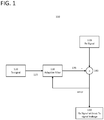
- FIG. 1 shows an adaptive filter diagram 100 in an aspect of this disclosure.
- adaptive filter diagram 100 is exemplary in nature and may therefore by simplified for purposes of this explanation.
- the ensuing explanation focuses on the application of the disclosed adaptive filter mechanism and methods to self-interference cancellation between transmit and receive equipment in a wireless device, but it is appreciated that the ensuing disclosure encompasses other adaptive filter applications, e.g. IM3 cancellation, digital pre-distortion, and 3G Radio Resource Control (RRC) equalization, as well.
- RRC Radio Resource Control
- the received signal (Rx signal) 110 includes the intended Rx signal (i.e. the signal as received at the device) plus interference produced by unknown signal leakage from the transmission equipment of the device (among other forms of interference).
- the transmitted signal 120 cannot simply be subtracted from the Rx signal 110 in order to recover the intended Rx signal because this would not account for the effects of signal leakage from components of the Rx/Tx chain (e.g. mixers, amplifiers, converters, etc.).
- an adaptive filter 130 is implemented to produce a more accurate representation of the signal leakage interference in the adaptive filter signal, i.e. cancellation signal, 135.
- This cancellation signal is then subtracted 140 from the Rx signal 110 in order to attempt to retrieve the intended Rx signal, i.e. the Rx signal without the Tx signal leakage, 150.
- This resulting signal is fed back to the adaptive filter 130 as an error so the adaptive filter 130 may update the cancellation signal 135 in the next iteration.
- FIR adaptive finite impulse response
- the focal point of the disclosure is the calculation of the step size (i.e. the weigh calculation applied in each iteration) of the adaptive filter.
- the step size ( ⁇ ) determines the magnitude of the change (i.e. "step") taken by the adaptive filter algorithm in iteratively determining a useful coefficient vector to be used in the next iteration (i.e. W ( n + 1)in Equation (1)) of cancellation signal 135.
- FIG. 2 provides a more detailed configuration for adaptive filter 130 in this disclosure.
- FIG. 2 shows a more detailed structure 200 for adaptive filter (i.e. for adaptive filter 130 ). It is appreciated that configuration 200 is exemplary in nature and may therefore be simplified for purposes of this explanation.
- Tx and Rx signals are composed of both in-phase and quadrature components, shown as ITX+jQTX 202 and IRX+jQRX 204, respectively.
- ITX+jQTX 202 is representative of Tx signal 120
- IRX+jQRX 204 is representative of Rx signal 110.
- the complex FIR sum 214 sums all of the components of adaptive filter structure 200 in order to produce cancellation signal 206.
- Complex filter taps 210-212 produce delays in adaptive filter structure 200 to determine the components to be summed by Complex FIR sum 214.
- the focal point of structure 200 as associated with this disclosure is in the weight (i.e. step size) determination performed for weight accumulators 220-224.
- the dashed lines are meant to provide depiction of the different stages of the adaptive filter structure 200.
- a variable step size ( ⁇ ) is determined in each iteration of Equation 1.
- the lesser of two elements is chosen as the step size ( ⁇ ) for that particular iteration.
- the first element ( ⁇ 1) is inversely proportional to a time (t). In other words, ⁇ 1 is a monotonically decreasing function as related to time, i.e. the number of iterations.
- the second element ( ⁇ 2) is determined from the power of the Tx signal. In other words, ⁇ 2 may be determined in similar fashion to the NLMS step size.
- the power calculation can be simplified by sum of the absolute values terms.
- a scaling of the time dependent step size ( ⁇ 1) may be implemented in order to account for interference and noise of the receive path.
- the scaling is chosen based on known or estimated Rx wanted level (or noise level or both) on the Rx input side.
- the scaling i.e. via the values of t 1 and m 1 ) decreases in order to provide optimal results.
- the step size determination for ⁇ may be numerically limited to a minimum and maximum step size, where the minimum is determined by the required accuracy and tracking performance in the settled state of the system, and the maximum is determined to be a value slightly larger than the expected maximum step size which would be determined in a strictly NLMS implementation.
- a cold/soft restart of the step size control may be employed, where the maximum step size of the control is dependent on changing signal conditions, e.g. the frequency allocation of the Tx signal. This, for example, may lead to a lower calculation for ⁇ 1.
- a blind tap is introduced, for example, in place of Complex FIR tap n 212.
- the ⁇ 1 step size may be realized by a 1/t decay, or more preferably, by a discrete step size table ( ⁇ Table) and its scaling can be controlled by additional parameters, such as interference and/or noise or if boundary conditions are changing (e.g. signal levels or signal types).
- ⁇ Table discrete step size table
- multipliers in error feedback can use barrel shifters (e.g. two shift values, one for time iteration [0,...,t1] and one for time iterations greater than t1) in order to avoid big multiplier word lengths, thereby minimizing hardware requirements.
- barrel shifters e.g. two shift values, one for time iteration [0,...,t1] and one for time iterations greater than t1
- FIG. 3 shows a hardware (HW) implementation 300 in an aspect of this disclosure. It is appreciated that HW implementation 300 is exemplary in nature and may therefore be simplified for purposes of this disclosure. It is also realized that alternate forms of HW implementation which achieve analogous results by implementing the step size calculations of this disclosure are encompassed by the explanation herein.
- HW hardware
- HW implementation 300 is similar to the configuration disclosed in FIG. 2 , and therefore, the same reference numbers refer to similar components.
- the aforementioned barrel shifters 342-344 are implemented in series with the XLMS weight accumulators 222-224 to avoid big multiplier word lengths and minimize hardware.
- the Complex blind FIR tap 312 is employed in lieu of Complex FIR tap n 212 of FIG. 2 to, in addition to realizing the once cycle delay of tap 210, to account for the compensating effect of the pipelined register 335, which is introduced for synchronizing combination logic which may be included in the cancellation signal 206, and therefore, find its way into the error feedback path 330.
- the XLMS step size algorithm is implemented into unit 301, which selects the lesser of the step sizes, ⁇ 1 and ⁇ 2, determined from the ⁇ Table (i.e. time-dependent) and the Tx Power (P), respectively.
- Control 302 may introduce other inputs to the XLMS step size unit 301. These inputs may include a cold/soft restart and/or a signal to interference ratio.
- a power detector may be implemented at the adaptive filter input (i.e. at 115 in FIG. 1 ), providing a Tx signal power check and switching the XLMS algorithm unit 301 to hold a coefficient state (i.e. stopping adaptation) if the Tx signal power is below a certain threshold.
- a coefficient state i.e. stopping adaptation
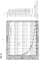
- FIG. 4 shows an exemplary ⁇ 1 step size table (i.e. graph) 400 with corresponding exemplary code 450. It is appreciated that graph 400 is exemplary in nature and may therefore be modified and still be encompassed within disclosure.
- the discrete step size table line (i.e. ⁇ 1 step size table) is indicated by the step line depicted in graph 400.
- This lines corresponds to the exemplary code 450. It represents a typical cold start (adaptive filter weights starting from zero).
- Code 450 depicts the manner in which a predetermined step size table may be selected. It is appreciated that a similar step size table, with a similar descending step-like (i.e. monotonically decreasing) relationship between the step size and the number of iterations may be implemented.
- the line marked by the circles represents 1/t behavior.
- the region outlined by line 410 and line 420 is the region where the NLMS is potentially limiting, and the area below line 420 is the area where the 1/t behavior limits the step size in order achieve higher accuracy and better adaptation (i.e. better cancellation in case of SIC).
- the minimum step size of ⁇ 1 is limited to line 430. In this manner, the smaller step sizes can be avoided in order to achieve faster convergence.
- a soft restart table for ⁇ 1 would lower line 410 (i.e. the upper step size limit) to the region between line 420 and line 430, assuming that the current adaptive filter weight state are not zero, but in fact closer to the optimum state.
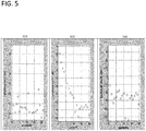
- FIG. 5 shows a comparison of the settling behavior of an NLMS algorithm 510, an LMS algorithm 520, and the XLMS algorithm 530 of this disclosure.
- the NLMS algorithm 510 shows good settling, but lacks the accuracy (i.e. the interference suppression) of the other signals are demonstrated by its spur power out/in ratio of about -11.5 dBs.
- the LMS algorithm 520 (with a constant step size of 1.0E-4) shows good accuracy demonstrated by its spur power out/in ration of about -17 dBs, but it also shows slow settling as evident in the slow convergence to its final state.
- the XLMS algorithm 530 shows both good settling and high accuracy when compared to 510 and 520.
- FIG. 6 is a graph 600 showing the settling performance of the XLMS algorithm of this disclosure for suppressing Tx spur in Rx signal for a low intended Rx signal using a 12-tap filter for adaption of multiple hundreds duplexer transfer functions, which results in the multiple hundred settling curves shown in graph 600.
- a full allocation of LTE20 was used for the Tx signal and for the Rx signal LTE10.
- the suppression was calculated by the spur power out/spur power in, where the modulated spur power is equal to the noise power plus the intended Rx signal.
- FIG. 7 shows a graph 700 depicting the settling performance of the XLMS algorithm of this disclosure for suppressing Tx spur in Rx signal for a high intended Rx signal.
- the Rx signal is 30 dB above Tx (LTE20) and the signal to interference ratio (SIR) is 30 dB, thereby implementing the adapted ⁇ 1 step size table.
- the measured data in graph 600 is the receiver signal.
- the spur in/out of the XLMS algorithm of this disclosure after 7 symbols is about - 2.2 dBs, signifying a +2.2 dB interference cancellation. After 80 symbols, it is -6.5 dBs, signifying a 6.5 dB interference cancellation.
- Chart 750 shows a comparison of the novel XLMS methods and mechanisms of this disclosure (in the second column) when compared to the highly computational complex RLS (in the first column) method in a high interference (30 dBs) scenario. Higher positive numbers indicate better results, with negative value indicating an increase in distortion, i.e. the cancellation circuit is counterproductive. As is clearly evident from chart 750, the XLMS method and mechanism of this disclosure achieves better results that the RLS algorithm at a lower computational complexity.
- FIG. 8 shows an internal configuration of user equipment (UE) 800, which may be configured to perform the adaptive filtering procedure of this disclosure.
- UE 800 may include antenna system 802, radio frequency (RF) transceiver 804, baseband modem 806 (including physical layer processing circuit 808 and controller 810 ), data source 812, memory 814, and data sink 816.
- RF radio frequency
- UE 800 may include one or more additional hardware, software, and/or firmware components (such as processors/microprocessors, controllers/microcontrollers, other specialty or generic hardware/processors/circuits, etc.), peripheral device(s), memory, power supply, external device interface(s), subscriber identify module(s) (SIMs), user input/output devices (display(s), keypad(s), touchscreen(s), speaker(s), external button(s), camera(s), microphone(s), etc.), etc.
- processors/microprocessors such as processors/microprocessors, controllers/microcontrollers, other specialty or generic hardware/processors/circuits, etc.
- peripheral device(s) such as processors/microprocessors, controllers/microcontrollers, other specialty or generic hardware/processors/circuits, etc.
- peripheral device(s) such as peripheral device(s), memory, power supply, external device interface(s), subscriber identify module(s) (SIMs), user input/output devices (disp
- UE 800 may transmit and receive radio signals on one or more RANs.
- Baseband modem 806 may direct such communication functionality of UE 800 according to the communication protocols associated with each RAN, and may execute control over antenna system 802 and RF transceiver 804 in order to transmit and receive radio signals according to the formatting and scheduling parameters defined by each communication protocol.
- UE 800 may transmit and receive radio signals with antenna system 802, which may be a single antenna or an antenna array composed of multiple antennas and may additionally include analog antenna combination and/or beamforming circuitry.
- the receive path (RX) of RF transceiver 804 may receive analog radio frequency signals from antenna system 802 and perform analog and digital RF front-end processing on the analog radio frequency signals to produce digital baseband samples (e.g. In-Phase/Quadrature (IQ) samples) to provide to baseband modem 806.
- RF transceiver 804 may accordingly include analog and digital reception circuitry including amplifiers (e.g. a Low Noise Amplifier (LNA), filters, RF demodulators (e.g.
- LNA Low Noise Amplifier
- RF transceiver 804 may receive digital baseband samples from baseband modem 806 and perform analog and digital RF front-end processing on the digital baseband samples to produce analog radio frequency signals to provide to antenna system 802 for wireless transmission.
- RF transceiver 804 may thus include analog and digital transmission circuitry including amplifiers (e.g. a Power Amplifier (PA), filters, RF modulators (e.g.
- PA Power Amplifier
- Baseband modem 806 may control the RF transmission and reception of RF transceiver 804, including specifying transmit and receive radio frequencies for operation of RF transceiver 804.
- baseband modem 806 may include physical layer processing circuit 808, which may perform physical layer (Layer 1) transmission and reception processing to prepare outgoing transmit data provided by controller 810 for transmission via RF transceiver 804 and prepare incoming received data provided by RF transceiver 804 for processing by controller 810.
- Physical layer processing circuit 810 may accordingly perform one or more of adaptive filtering, error detection, forward error correction encoding/decoding, channel coding and interleaving, physical channel modulation/demodulation, physical channel mapping, radio measurement and search, frequency and time synchronization, antenna diversity processing, power control and weighting, rate matching, retransmission processing, etc.
- Physical layer processing circuit 808 may be structurally realized as hardware logic, e.g.
- physical layer processing circuit 808 may include a control circuit such as a processor configured to control the various hardware and software processing components of physical layer processing circuit 808 in accordance with physical layer control logic defined by the communications protocol for the relevant radio access technologies (RATs).
- RATs radio access technologies
- Physical layer processing circuit 808 may include hardware and/or software to implement the adaptive filtering methods of this disclosure, e.g. as described in the other figures.
- UE 800 may be configured to operate according to one or more RATs, which may be directed by controller 810. Controller 810 may thus be responsible for controlling the radio communication components of UE 800 (antenna system 802, RF transceiver 804, and physical layer processing circuit 808 ) in accordance with the communication protocols of each supported RAT, and accordingly may represent the Access Stratum (AS) and Non-Access Stratum (NAS) (also encompassing Layer 2 and Layer 3) of each supported RAT. Controller 810 may be structurally embodied as a protocol processor configured to execute protocol software (retrieved from controller memory MEM as shown in FIG. 4 ) and subsequently control the radio communication components of UE 800 in order to transmit and receive communication signals in accordance with the corresponding protocol control logic defined in the protocol software.
- protocol software retrieved from controller memory MEM as shown in FIG. 4
- Controller 810 may therefore be configured to manage the radio communication functionality of UE 800 in order to communicate with the various radio and core network components of a radio communication network, and accordingly may be configured according to the communication protocols for both the LTE network and the GSM/UMTS legacy network.
- Controller 810 may either be a unified controller that is collectively responsible for all supported RATs (e.g. LTE and GSM/UMTS) or may be composed of multiple separate controllers where each controller is a dedicated controller for a particular RAT, such as e.g. a dedicated LTE controller and a dedicated legacy controller (or alternatively a dedicated LTE controller, dedicated GSM controller, and a dedicated UMTS controller).
- controller 810 may be responsible for directing radio communication activity of UE 800 according to the communication protocols of the LTE and legacy networks.
- one or both of antenna system 802 and RF transceiver 804 may similarly be partitioned into multiple dedicated components that each respectively correspond to one or more of the supported RATs.
- controller 810 may be configured to control the radio communication operations of UE 800 in accordance with a master/slave RAT hierarchical or multi-SIM scheme.
- UE 800 may further comprise data source 812, memory 814, and data sink 816, where data source 812 may include sources of communication data above controller 810 (i.e. above the NAS/Layer 3) and data sink 816 may include destinations of communication data above controller 810 (i.e. above the NAS/Layer 3).
- data source 812 may include sources of communication data above controller 810 (i.e. above the NAS/Layer 3) and data sink 816 may include destinations of communication data above controller 810 (i.e. above the NAS/Layer 3).
- Such may include, for example, an application processor of UE 800, which may be configured to execute various applications and/or programs of UE 800 at an application layer of UE 800, such as e.g. an Operating System (OS), a User Interface (UI) for supporting user interaction with UE 800, and/or various user applications.
- OS Operating System
- UI User Interface
- the application processor may interface with baseband modem 806 (as data source 812 /data sink 816 ) as an application layer to transmit and receive user data such as voice data, audio/video/image data, messaging data, application data, basic Internet/web access data, etc., over a the radio network connection(s) provided by baseband modem 806.
- Data source 812 and data sink 816 may additionally represent various user input/output devices of UE 800, such as display(s), keypad(s), touchscreen(s), speaker(s), external button(s), camera(s), microphone(s), etc., which may allow a user of UE 800 to control various communication functions of UE 800 associated with user data.
- Memory 814 may embody a memory component of UE 800, such as e.g. a hard drive or another such permanent memory device. Although not explicitly depicted in FIG. 8 , the various other components of UE 800 shown in FIG. 8 may additionally each include integrated permanent and non-permanent memory components, such as for storing software program code, buffering data, etc.
- FIG. 9 shows a flowchart 900 detailing an adaptive filter method in an aspect of this disclosure. It is appreciated that flowchart 900 is exemplary in nature and may therefore be simplified for purposes of this explanation.
- the adaptive filtering method described in flowchart 900 may be implemented by the physical processing layer circuit 808 of UE 800 in FIG. 8 in order to determine a step size (i.e. weight) for each iteration of an adaptive filtering process.
- a first element is determined which monotonically decreases over the number of iterations 902. For example, as the number of the iterations increases (i.e. as time increases), the first element will either decrease or stay the same (i.e. is monotonic in nature).
- a second element is determined (i.e. calculated) from a power of the first input signal to the adaptive filter 904.
- the first input signal may be, for example, the transmitted signal from the communication device which is interfering with the received signal.
- the adaptive filtering process disclosed herein is implemented in order to mimic the leakage of the transmitted signal into the received signal (in the transceiver and the physical processing layer circuit) in order to remove said leakage.
- 902 and 904 may be switched or they may be performed simultaneously.
- the lesser of the two is chosen as the step size for that particular iteration of the adaptive filtering process 906.
- Example 1 a circuitry for determining an adaptive filter step size for processing a received signal, the circuitry including an adaptive filter circuit configured to receive a first input signal and produce a variable cancellation signal, wherein a step size for each iteration of the variable cancellation signal is the lesser of a first element which monotonically decreases over the number of iterations; or a second element calculated from a power of the first input signal; and an evaluation circuit configured to subtract the variable cancellation signal from the received signal to generate a second input signal, wherein the adaptive filter circuit adjusts the variable cancellation signal based on the second input signal.
- an adaptive filter circuit configured to receive a first input signal and produce a variable cancellation signal, wherein a step size for each iteration of the variable cancellation signal is the lesser of a first element which monotonically decreases over the number of iterations; or a second element calculated from a power of the first input signal
- an evaluation circuit configured to subtract the variable cancellation signal from the received signal to generate a second input signal, wherein the adaptive filter circuit adjusts the variable cancellation signal based on
- Example 2 the subject matter of Example 1 may include wherein the first element is determined by a function which is inversely proportional to the number of iterations.
- Example 3 the subject matter of Example 1 may include wherein the first element is determined by a predetermined step size table.
- Example 4 the subject matter of Examples 1-3 may include wherein the second element is limited by a normalized least mean squares step size.
- Example 5 the subject matter of Examples 1-4 may include wherein the power of the first input signal is determined by the sum of the absolute value of its terms.
- Example 6 the subject matter of Examples 1-5 may include wherein a scalar is applied to the first element.
- Example 7 the subject matter of Example 6 may include wherein the scalar is dependent on an interference and/or a noise of the received signal.
- Example 9 the subject matter of Examples 1-8 may include wherein the step size is further limited by a minimum and maximum step size.
- Example 10 the subject matter of Example 9 may include wherein the minimum step size is determined by a predetermined required accuracy and tracking performance of the circuit in a settled state.
- Example 11 the subject matter of Examples 9-10 may include wherein the maximum step size is determined by an expected maximum of the second element.
- Example 12 the subject matter of Example 11 may include wherein a maximum of the first element is larger than the expected maximum of the second element.
- Example 13 the subject matter of Examples 1-12 may include the adaptive filter comprising barrel shifters, wherein each barrel shifter comprises a shift value.
- Example 14 the subject matter of Example 13 may include the barrel shifters configured to provide multipliers in the second input signal feedback with shift values.
- Example 15 the subject matter of Examples 13-14 may include wherein a first barrel shifter comprises a shift value for time iterations between 0 and tb, inclusive of tb.
- Example 16 the subject matter of Examples 13-15 may include wherein a second barrel shifter comprises a second shift value for time iterations greater than tb.
- Example 17 the subject matter of Examples 1-16 may include the adaptive filter comprising a complex FIR unit configured to receive as input a plurality of outputs from registers from within the adaptive filter and output the variable cancellation signal.
- the adaptive filter comprising a complex FIR unit configured to receive as input a plurality of outputs from registers from within the adaptive filter and output the variable cancellation signal.
- Example 18 the subject matter of Examples 1-17 may include the adaptive filter comprising one or more complex FIR taps configured to implement a one cycle delay.
- Example 19 the subject matter of Examples 1-18 may include the adaptive filter comprising at least one complex FIR blind tap configured to implement a compensating effect of a pipelined register in the circuitry.
- Example 20 the subject matter of Examples 1-19 may include a power detector configured to detect the power of the first input signal.
- Example 21 the subject matter of Example 20 may include wherein the power detector is further configured to stop the adaptive filter from producing the variable cancellation signal if the first input signal falls below a certain threshold.
- Example 22 the subject matter of Examples 1-21 may include wherein the circuitry is in a signal processing component of a communication device.
- Example 23 the subject matter of Examples 1-22 may include an input circuit configured to provide the first input signal to the adaptive filter unit.
- Example 24 the subject matter of Examples 1-23 may include wherein the first input signal is a transmission signal of a communication device.
- Example 25 the subject matter of Examples 1-24 may include wherein the circuitry is implemented as a self-interference cancellation (SIC) circuit in a communication device with duplex mode capabilities.
- SIC self-interference cancellation
- Example 26 the subject matter of Examples 1-25 may include wherein the circuity performs a time domain equalization in a communication device.
- a communication device including a transceiver configured to receive a signal from a network; and a baseband processing component, including an adaptive filter circuit, configured to: receive a first input signal and produce a variable cancellation signal, wherein a step size for each iteration of the variable cancellation signal is the lesser of: a first element which monotonically decreases over the number of iterations; or a second element calculated from a power of the first input signal; and subtract the variable cancellation signal from the signal received from the network to generate a second input signal; and control the adaptive filter circuit to adjust the variable cancellation signal based on the second input signal.
- Example 28 the subject matter of Example 27 may include wherein the first element is determined by a function which is inversely proportional to the number of the iteration.
- Example 29 the subject matter of Example 27 may include wherein the first element is determined by a predetermined step size table.
- Example 30 the subject matter of Examples 27-29 may include wherein the second element is limited by a normalized least mean squares step size.
- Example 31 the subject matter of Examples 27-30 may include wherein the power of the first input signal is determined by the sum of the absolute value of its terms.
- Example 32 the subject matter of Examples 27-31 may include wherein a scalar is applied to the first element.
- Example 33 the subject matter of Example 32 may include wherein the scalar is dependent on an interference and/or a noise of the signal received from the network.
- Example 35 the subject matter of Examples 27-34 may include wherein the step size is further limited by a minimum and maximum step size.
- Example 36 the subject matter of Example 35 may include wherein the minimum step size is determined by a predetermined required accuracy and tracking performance of the circuit in a settled state.
- Example 37 the subject matter of Examples 35-36 may include wherein the maximum step size is determined by an expected maximum of the second element.
- Example 38 the subject matter of Example 37 may include wherein a maximum of the first element is larger than the expected maximum of the second element.
- Example 39 the subject matter of Examples 27-38 may include the adaptive filter comprising barrel shifters, wherein each barrel shifter comprises a shift value.
- Example 40 the subject matter of Example 39 may include the barrel shifters configured to provide multipliers in the second input signal feedback with shift values.
- Example 41 the subject matter of Examples 39-40 may include wherein a first barrel shifter comprises a shift value for time iterations between 0 and tb, inclusive of tb.
- Example 42 the subject matter of Examples 39-41 may include wherein a second barrel shifter comprises a second shift value for time iterations greater than tb.
- Example 43 the subject matter of Examples 27-42 may include the adaptive filter comprising a complex FIR unit configured to receive as input a plurality of outputs from registers from within the adaptive filter and output the variable cancellation signal.
- the adaptive filter comprising a complex FIR unit configured to receive as input a plurality of outputs from registers from within the adaptive filter and output the variable cancellation signal.
- Example 44 the subject matter of Examples 27-43 may include the adaptive filter comprising one or more complex FIR taps configured to implement a one cycle delay.
- Example 45 the subject matter of Examples 27-44 may include the adaptive filter comprising at least one complex FIR blind tap configured to implement a compensating effect of a pipelined register in the circuitry.
- Example 46 the subject matter of Examples 27-45 may include further comprising a power detector configured to detect the power of the first input signal.
- Example 47 the subject matter of Example 46 may include wherein the power detector is further configured to stop the adaptive filter from producing the variable cancellation signal if the first input signal falls below a certain threshold.
- Example 48 the subject matter of Examples 27-47 may include wherein the circuitry is in a signal processing component of a communication device.
- Example 49 the subject matter of Examples 27-48 may include an input circuit configured to provide the first input signal to the adaptive filter unit.
- Example 50 the subject matter of Examples 27-49 may include wherein the first input signal is a transmission signal of a communication device.
- Example 51 the subject matter of Examples 27-50 may include wherein the circuitry is implemented as a self-interference cancellation (SIC) circuit in a communication device with duplex mode capabilities.
- SIC self-interference cancellation
- Example 52 the subject matter of Examples 27-51 may include wherein the baseband processing component performs a time domain equalization in a communication device.
- Example 53 the subject matter of Example 52 may include wherein a CDMA component of the baseband processing component performs the time domain equalization.
- Example 54 a method for determining a step size for each iteration of a variable cancellation signal of produced by an adaptive filter in a processing circuitry of a communication device, the method including: determining a first element which monotonically decreases over the number of iterations; determining a second element based on a power of a first input signal to the adaptive filter; and choosing the lesser of the first element and the second element as the step size for the iteration.
- Example 55 the subject matter of Example 54 may include determining the first element by a function which is inversely proportional to the number of the iteration.
- Example 56 the subject matter of Example 54 may include determining the first element with a predetermined step size table.
- Example 57 the subject matter of Examples 54-56 may include limiting the second element by a normalized least mean squares step size.
- Example 58 the subject matter of Examples 54-57 may include determining the power of the first input signal by the sum of the absolute value of its terms.
- Example 59 the subject matter of Examples 54-58 may include applying a scalar to the first element.
- Example 60 the subject matter of Example 59 may include wherein the scalar is dependent on an interference and/or a noise of a signal received at the communication device.
- Example 62 the subject matter of Examples 54-61 may include limiting the step size by a minimum and maximum step size.
- Example 63 the subject matter of Example 62 may include determining the minimum step size by a predetermined required accuracy and tracking performance of the circuit in a settled state.
- Example 64 the subject matter of Examples 62-63 may include determining the maximum step size by an expected maximum of the second element.
- Example 65 the subject matter of Example 64 may include wherein a maximum step size of the first element is larger than the expected maximum of the second element.
- Example 66 the subject matter of Examples 64-65 may include providing barrel shifters to provide multipliers of the second input signal feedback of the adaptive filter with shift values.
- Example 67 the subject matter of Example 66 may include wherein a first barrel shifter comprises a shift value for time iterations between 0 and tb, inclusive of tb.
- Example 68 the subject matter of Examples 66-67 may include wherein a second barrel shifter comprises a second shift value for time iterations greater than tb.
- Example 69 the subject matter of Examples 54-68 may include providing a power detector configured to detect the power of the first input signal.
- Example 70 the subject matter of Example 69 may include configuring the power detector to stop the adaptive filter from producing the variable cancellation signal if the first input signal falls below a certain threshold.
- Example 71 a computer readable medium with program instructions when executed cause a processor of a device to implement a method or realize an apparatus as claimed in any preceding Example.
- a device corresponding to a method detailed herein may include one or more components configured to perform each aspect of the related method.
Landscapes
- Noise Elimination (AREA)
Claims (15)
- Circuits (100) de détermination d'une taille de pas de filtre adaptatif pour traiter un signal reçu (110), les circuits comprenant :un circuit de filtre adaptatif (130) configuré pour recevoir un premier signal d'entrée (120) et produire un signal de suppression variable (135), dans lequel une taille de pas de chaque itération du signal de suppression variable est la plus petite :d'une première option de taille de pas qui décroît de façon monotone durant le nombre d'itérations (400) ; oud'une seconde option de taille de pas calculée à partir d'une puissance du premier signal d'entrée ; etun circuit d'évaluation (140) configuré pour soustraire le signal de suppression variable (135) du signal reçu (110) pour générer un second signal d'entrée (150), le circuit de filtre adaptatif (130) ajustant le signal de suppression variable (135) en fonction du second signal d'entrée (150).
- Circuits selon la revendication 1, dans lesquels la première option de taille de pas est déterminée par une fonction inversement proportionnelle au nombre d'itérations.
- Circuits selon la revendication 1, dans lesquels la première option de taille de pas est déterminée par une table de tailles de pas prédéterminée.
- Circuits selon l'une quelconque des revendications 1 à 3, dans lesquels la seconde option de taille de pas est limitée par une taille de pas par les moindres carrés normalisée.
- Circuits selon l'une quelconque des revendications 1 à 4, dans lesquels un scalaire est appliqué à la première option de taille de pas.
- Circuits selon la revendication 5, dans lesquels le scalaire dépend d'un brouillage et/ou d'un bruit du signal reçu.
- Circuits selon l'une quelconque des revendications 5 et 6, dans lesquels le scalaire est représenté par la formule :

- Circuits selon l'une quelconque des revendications 1 à 7, dans lesquels la taille de pas est limitée en outre par une taille de pas minimale et maximale.
- Circuits selon l'une quelconque des revendications 1 à 8, le filtre adaptatif comprenant des circuits de décalage circulaire, chaque circuit de décalage circulaire comprenant une valeur de décalage.
- Circuits selon l'une quelconque des revendications 1 à 9, les circuits se trouvant dans un composant de traitement de signaux d'un dispositif de communications.
- Procédé de détermination d'une taille de pas de chaque itération d'un signal de suppression variable (135) produit par un filtre adaptatif (130) dans des circuits de traitement d'un dispositif, le procédé comprenant :la détermination d'une première option de taille de pas qui décroît de façon monotone durant le nombre d'itérations ;la détermination d'une seconde option de taille de pas en fonction d'une puissance d'un premier signal d'entrée (120) du filtre adaptatif (130) ; etle choix de la plus petite de la première option de taille de pas et de la seconde option de taille de pas comme taille de pas de l'itération.
- Procédé selon la revendication 11, comprenant en outre de la détermination de la première option de taille de pas par une fonction inversement proportionnelle au nombre d'itérations.
- Procédé selon la revendication 11, comprenant en outre la détermination de la première option de taille de pas avec une table de tailles de pas prédéterminée.
- Procédé selon l'une quelconque des revendications 11 à 13, comprenant en outre l'application d'un scalaire à la première option de taille de pas.
- Mémoire lisible par machine comportant des instructions lisibles par machines qui, à leur exécution, mettent en oeuvre un procédé ou réalisent des circuits selon l'une quelconque des revendications précédentes.
Priority Applications (2)
| Application Number | Priority Date | Filing Date | Title |
|---|---|---|---|
| EP16191469.2A EP3301810B1 (fr) | 2016-09-29 | 2016-09-29 | Circuits et procédés de filtre adaptatif |
| PCT/US2017/046401 WO2018063526A1 (fr) | 2016-09-29 | 2017-08-11 | Circuits de filtre adaptatif et procédés associés |
Applications Claiming Priority (1)
| Application Number | Priority Date | Filing Date | Title |
|---|---|---|---|
| EP16191469.2A EP3301810B1 (fr) | 2016-09-29 | 2016-09-29 | Circuits et procédés de filtre adaptatif |
Publications (2)
| Publication Number | Publication Date |
|---|---|
| EP3301810A1 EP3301810A1 (fr) | 2018-04-04 |
| EP3301810B1 true EP3301810B1 (fr) | 2019-02-13 |
Family
ID=57211252
Family Applications (1)
| Application Number | Title | Priority Date | Filing Date |
|---|---|---|---|
| EP16191469.2A Active EP3301810B1 (fr) | 2016-09-29 | 2016-09-29 | Circuits et procédés de filtre adaptatif |
Country Status (2)
| Country | Link |
|---|---|
| EP (1) | EP3301810B1 (fr) |
| WO (1) | WO2018063526A1 (fr) |
Families Citing this family (1)
| Publication number | Priority date | Publication date | Assignee | Title |
|---|---|---|---|---|
| CN115842532A (zh) * | 2022-12-21 | 2023-03-24 | 哲库科技(上海)有限公司 | 信号滤波方法、装置以及电子设备 |
Family Cites Families (10)
| Publication number | Priority date | Publication date | Assignee | Title |
|---|---|---|---|---|
| US5058047A (en) * | 1989-05-30 | 1991-10-15 | Advanced Micro Devices, Inc. | System and method for providing digital filter coefficients |
| US6917688B2 (en) * | 2002-09-11 | 2005-07-12 | Nanyang Technological University | Adaptive noise cancelling microphone system |
| US7233164B2 (en) * | 2003-12-17 | 2007-06-19 | Rambus Inc. | Offset cancellation in a multi-level signaling system |
| US7533140B2 (en) * | 2004-04-13 | 2009-05-12 | Jaber Associates, L.L.C. | Method and apparatus for enhancing processing speed for performing a least mean square operation by parallel processing |
| US8385397B2 (en) * | 2007-01-19 | 2013-02-26 | Techwell Llc | Method for determining the step size for an LMS adaptive equalizer for 8VSB |
| US9231561B2 (en) * | 2011-12-30 | 2016-01-05 | Intel Corporation | Multi-stage adaptive filter |
| US9252831B2 (en) * | 2013-03-01 | 2016-02-02 | Qualcomm Incorporated | Multi-tap adaptive filter for transmit signal leakage cancellation |
| US9306654B2 (en) * | 2014-01-10 | 2016-04-05 | Qualcomm Incorporated | Opportunistic active interference cancellation using RX diversity antenna |
| KR101500922B1 (ko) * | 2015-01-12 | 2015-03-18 | 포항공과대학교 산학협력단 | 적응필터를 이용한 분산 추정방법 및 장치 |
| US9407298B1 (en) * | 2015-03-05 | 2016-08-02 | Qualcomm Incorporated | Radio frequency (RF) analog interference cancellation (AIC) with multiple antennas |
-
2016
- 2016-09-29 EP EP16191469.2A patent/EP3301810B1/fr active Active
-
2017
- 2017-08-11 WO PCT/US2017/046401 patent/WO2018063526A1/fr not_active Ceased
Non-Patent Citations (1)
| Title |
|---|
| None * |
Also Published As
| Publication number | Publication date |
|---|---|
| EP3301810A1 (fr) | 2018-04-04 |
| WO2018063526A1 (fr) | 2018-04-05 |
Similar Documents
| Publication | Publication Date | Title |
|---|---|---|
| EP3273606B1 (fr) | Dispositifs et procédés d'annulation d'autobrouillage | |
| TWI479810B (zh) | 適應性輸入相關二階截點校準 | |
| Anttila et al. | Full-duplexing with SDR devices: Algorithms, FPGA implementation, and real-time results | |
| US10284356B2 (en) | Self-interference cancellation | |
| EP3499744B1 (fr) | Récepteur en diversité, et terminal | |
| US9712369B2 (en) | Method and apparatus for low-complexity frequency dependent IQ imbalance compensation | |
| US20150065058A1 (en) | Non-linear interference cancellation with multiple aggressors | |
| US10277381B2 (en) | Receiver path distortion mitigation using adaptive filter feedback | |
| EP2876853B1 (fr) | Prédistorsion numérique adaptative de bande passante étendue avec des entrées analogiques reconfigurables | |
| WO2016164183A1 (fr) | Annulation d'auto-brouillage à l'aide d'un filtre numérique et d'un récepteur auxiliaire | |
| JP2012147455A (ja) | ノイズの多い推定値をフィルタリングして推定誤差を低減するための方法および装置 | |
| CN109644013A (zh) | 用于自干扰消除的发射机波束成形 | |
| EP3133787B1 (fr) | Filtres à durée continue de retard d'unité de quart et de coefficients de pondération complexe | |
| WO2007054538A1 (fr) | Filtre et procede permettant de supprimer les effets d'interference de voies adjacentes | |
| WO2014210518A1 (fr) | Annulation de brouillage radioélectrique tout analogique et hybride utilisant des câbles, des atténuateurs et des répartiteurs de puissance | |
| JP4773294B2 (ja) | 適応等化装置及び受信装置 | |
| EP3301810B1 (fr) | Circuits et procédés de filtre adaptatif | |
| US20100060523A1 (en) | Adaptive array antenna apparatus and adaptive control method therefor | |
| WO2016191072A1 (fr) | Auto-annulation d'interférence active robuste en présence de signaux intra-bande externes à l'aide de mesures de signal de région de garde | |
| US10211931B1 (en) | Method of interference cancellation and transceiving device | |
| US20180159585A1 (en) | A receiver and a method for reducing a distortion component within a baseband receive signal | |
| US8812571B2 (en) | Spectrum agile radio | |
| CN109586758B (zh) | 干扰消除方法及传收装置 | |
| Choi et al. | Self-Interference Cancellation and Turbo Equalizer Design for the Single-band Full Duplex System using Single Antenna | |
| WO2017132949A1 (fr) | Procédé et émetteur-récepteur radio de duplexage à répartition dans le temps (tdd) pour corriger une défaillance en phase et en quadrature (iq) de réception |
Legal Events
| Date | Code | Title | Description |
|---|---|---|---|
| PUAI | Public reference made under article 153(3) epc to a published international application that has entered the european phase |
Free format text: ORIGINAL CODE: 0009012 |
|
| STAA | Information on the status of an ep patent application or granted ep patent |
Free format text: STATUS: REQUEST FOR EXAMINATION WAS MADE |
|
| 17P | Request for examination filed |
Effective date: 20160929 |
|
| AK | Designated contracting states |
Kind code of ref document: A1 Designated state(s): AL AT BE BG CH CY CZ DE DK EE ES FI FR GB GR HR HU IE IS IT LI LT LU LV MC MK MT NL NO PL PT RO RS SE SI SK SM TR |
|
| AX | Request for extension of the european patent |
Extension state: BA ME |
|
| GRAP | Despatch of communication of intention to grant a patent |
Free format text: ORIGINAL CODE: EPIDOSNIGR1 |
|
| STAA | Information on the status of an ep patent application or granted ep patent |
Free format text: STATUS: GRANT OF PATENT IS INTENDED |
|
| INTG | Intention to grant announced |
Effective date: 20180730 |
|
| GRAS | Grant fee paid |
Free format text: ORIGINAL CODE: EPIDOSNIGR3 |
|
| GRAJ | Information related to disapproval of communication of intention to grant by the applicant or resumption of examination proceedings by the epo deleted |
Free format text: ORIGINAL CODE: EPIDOSDIGR1 |
|
| GRAL | Information related to payment of fee for publishing/printing deleted |
Free format text: ORIGINAL CODE: EPIDOSDIGR3 |
|
| STAA | Information on the status of an ep patent application or granted ep patent |
Free format text: STATUS: REQUEST FOR EXAMINATION WAS MADE |
|
| GRAR | Information related to intention to grant a patent recorded |
Free format text: ORIGINAL CODE: EPIDOSNIGR71 |
|
| STAA | Information on the status of an ep patent application or granted ep patent |
Free format text: STATUS: GRANT OF PATENT IS INTENDED |
|
| INTC | Intention to grant announced (deleted) | ||
| GRAA | (expected) grant |
Free format text: ORIGINAL CODE: 0009210 |
|
| STAA | Information on the status of an ep patent application or granted ep patent |
Free format text: STATUS: THE PATENT HAS BEEN GRANTED |
|
| INTG | Intention to grant announced |
Effective date: 20190103 |
|
| AK | Designated contracting states |
Kind code of ref document: B1 Designated state(s): AL AT BE BG CH CY CZ DE DK EE ES FI FR GB GR HR HU IE IS IT LI LT LU LV MC MK MT NL NO PL PT RO RS SE SI SK SM TR |
|
| REG | Reference to a national code |
Ref country code: GB Ref legal event code: FG4D |
|
| REG | Reference to a national code |
Ref country code: CH Ref legal event code: EP Ref country code: AT Ref legal event code: REF Ref document number: 1096806 Country of ref document: AT Kind code of ref document: T Effective date: 20190215 |
|
| REG | Reference to a national code |
Ref country code: IE Ref legal event code: FG4D |
|
| REG | Reference to a national code |
Ref country code: DE Ref legal event code: R096 Ref document number: 602016009899 Country of ref document: DE |
|
| REG | Reference to a national code |
Ref country code: NL Ref legal event code: FP |
|
| REG | Reference to a national code |
Ref country code: LT Ref legal event code: MG4D |
|
| PG25 | Lapsed in a contracting state [announced via postgrant information from national office to epo] |
Ref country code: LT Free format text: LAPSE BECAUSE OF FAILURE TO SUBMIT A TRANSLATION OF THE DESCRIPTION OR TO PAY THE FEE WITHIN THE PRESCRIBED TIME-LIMIT Effective date: 20190213 Ref country code: NO Free format text: LAPSE BECAUSE OF FAILURE TO SUBMIT A TRANSLATION OF THE DESCRIPTION OR TO PAY THE FEE WITHIN THE PRESCRIBED TIME-LIMIT Effective date: 20190513 Ref country code: SE Free format text: LAPSE BECAUSE OF FAILURE TO SUBMIT A TRANSLATION OF THE DESCRIPTION OR TO PAY THE FEE WITHIN THE PRESCRIBED TIME-LIMIT Effective date: 20190213 Ref country code: FI Free format text: LAPSE BECAUSE OF FAILURE TO SUBMIT A TRANSLATION OF THE DESCRIPTION OR TO PAY THE FEE WITHIN THE PRESCRIBED TIME-LIMIT Effective date: 20190213 Ref country code: PT Free format text: LAPSE BECAUSE OF FAILURE TO SUBMIT A TRANSLATION OF THE DESCRIPTION OR TO PAY THE FEE WITHIN THE PRESCRIBED TIME-LIMIT Effective date: 20190613 |
|
| PG25 | Lapsed in a contracting state [announced via postgrant information from national office to epo] |
Ref country code: IS Free format text: LAPSE BECAUSE OF FAILURE TO SUBMIT A TRANSLATION OF THE DESCRIPTION OR TO PAY THE FEE WITHIN THE PRESCRIBED TIME-LIMIT Effective date: 20190613 Ref country code: LV Free format text: LAPSE BECAUSE OF FAILURE TO SUBMIT A TRANSLATION OF THE DESCRIPTION OR TO PAY THE FEE WITHIN THE PRESCRIBED TIME-LIMIT Effective date: 20190213 Ref country code: HR Free format text: LAPSE BECAUSE OF FAILURE TO SUBMIT A TRANSLATION OF THE DESCRIPTION OR TO PAY THE FEE WITHIN THE PRESCRIBED TIME-LIMIT Effective date: 20190213 Ref country code: GR Free format text: LAPSE BECAUSE OF FAILURE TO SUBMIT A TRANSLATION OF THE DESCRIPTION OR TO PAY THE FEE WITHIN THE PRESCRIBED TIME-LIMIT Effective date: 20190514 Ref country code: RS Free format text: LAPSE BECAUSE OF FAILURE TO SUBMIT A TRANSLATION OF THE DESCRIPTION OR TO PAY THE FEE WITHIN THE PRESCRIBED TIME-LIMIT Effective date: 20190213 Ref country code: BG Free format text: LAPSE BECAUSE OF FAILURE TO SUBMIT A TRANSLATION OF THE DESCRIPTION OR TO PAY THE FEE WITHIN THE PRESCRIBED TIME-LIMIT Effective date: 20190513 |
|
| REG | Reference to a national code |
Ref country code: AT Ref legal event code: MK05 Ref document number: 1096806 Country of ref document: AT Kind code of ref document: T Effective date: 20190213 |
|
| PG25 | Lapsed in a contracting state [announced via postgrant information from national office to epo] |
Ref country code: ES Free format text: LAPSE BECAUSE OF FAILURE TO SUBMIT A TRANSLATION OF THE DESCRIPTION OR TO PAY THE FEE WITHIN THE PRESCRIBED TIME-LIMIT Effective date: 20190213 Ref country code: DK Free format text: LAPSE BECAUSE OF FAILURE TO SUBMIT A TRANSLATION OF THE DESCRIPTION OR TO PAY THE FEE WITHIN THE PRESCRIBED TIME-LIMIT Effective date: 20190213 Ref country code: EE Free format text: LAPSE BECAUSE OF FAILURE TO SUBMIT A TRANSLATION OF THE DESCRIPTION OR TO PAY THE FEE WITHIN THE PRESCRIBED TIME-LIMIT Effective date: 20190213 Ref country code: CZ Free format text: LAPSE BECAUSE OF FAILURE TO SUBMIT A TRANSLATION OF THE DESCRIPTION OR TO PAY THE FEE WITHIN THE PRESCRIBED TIME-LIMIT Effective date: 20190213 Ref country code: RO Free format text: LAPSE BECAUSE OF FAILURE TO SUBMIT A TRANSLATION OF THE DESCRIPTION OR TO PAY THE FEE WITHIN THE PRESCRIBED TIME-LIMIT Effective date: 20190213 Ref country code: IT Free format text: LAPSE BECAUSE OF FAILURE TO SUBMIT A TRANSLATION OF THE DESCRIPTION OR TO PAY THE FEE WITHIN THE PRESCRIBED TIME-LIMIT Effective date: 20190213 Ref country code: SK Free format text: LAPSE BECAUSE OF FAILURE TO SUBMIT A TRANSLATION OF THE DESCRIPTION OR TO PAY THE FEE WITHIN THE PRESCRIBED TIME-LIMIT Effective date: 20190213 Ref country code: AL Free format text: LAPSE BECAUSE OF FAILURE TO SUBMIT A TRANSLATION OF THE DESCRIPTION OR TO PAY THE FEE WITHIN THE PRESCRIBED TIME-LIMIT Effective date: 20190213 |
|
| REG | Reference to a national code |
Ref country code: DE Ref legal event code: R097 Ref document number: 602016009899 Country of ref document: DE |
|
| PG25 | Lapsed in a contracting state [announced via postgrant information from national office to epo] |
Ref country code: PL Free format text: LAPSE BECAUSE OF FAILURE TO SUBMIT A TRANSLATION OF THE DESCRIPTION OR TO PAY THE FEE WITHIN THE PRESCRIBED TIME-LIMIT Effective date: 20190213 Ref country code: SM Free format text: LAPSE BECAUSE OF FAILURE TO SUBMIT A TRANSLATION OF THE DESCRIPTION OR TO PAY THE FEE WITHIN THE PRESCRIBED TIME-LIMIT Effective date: 20190213 |
|
| PLBE | No opposition filed within time limit |
Free format text: ORIGINAL CODE: 0009261 |
|
| STAA | Information on the status of an ep patent application or granted ep patent |
Free format text: STATUS: NO OPPOSITION FILED WITHIN TIME LIMIT |
|
| PG25 | Lapsed in a contracting state [announced via postgrant information from national office to epo] |
Ref country code: AT Free format text: LAPSE BECAUSE OF FAILURE TO SUBMIT A TRANSLATION OF THE DESCRIPTION OR TO PAY THE FEE WITHIN THE PRESCRIBED TIME-LIMIT Effective date: 20190213 |
|
| 26N | No opposition filed |
Effective date: 20191114 |
|
| PG25 | Lapsed in a contracting state [announced via postgrant information from national office to epo] |
Ref country code: SI Free format text: LAPSE BECAUSE OF FAILURE TO SUBMIT A TRANSLATION OF THE DESCRIPTION OR TO PAY THE FEE WITHIN THE PRESCRIBED TIME-LIMIT Effective date: 20190213 |
|
| PG25 | Lapsed in a contracting state [announced via postgrant information from national office to epo] |
Ref country code: TR Free format text: LAPSE BECAUSE OF FAILURE TO SUBMIT A TRANSLATION OF THE DESCRIPTION OR TO PAY THE FEE WITHIN THE PRESCRIBED TIME-LIMIT Effective date: 20190213 |
|
| PG25 | Lapsed in a contracting state [announced via postgrant information from national office to epo] |
Ref country code: MC Free format text: LAPSE BECAUSE OF FAILURE TO SUBMIT A TRANSLATION OF THE DESCRIPTION OR TO PAY THE FEE WITHIN THE PRESCRIBED TIME-LIMIT Effective date: 20190213 |
|
| REG | Reference to a national code |
Ref country code: CH Ref legal event code: PL |
|
| PG25 | Lapsed in a contracting state [announced via postgrant information from national office to epo] |
Ref country code: LU Free format text: LAPSE BECAUSE OF NON-PAYMENT OF DUE FEES Effective date: 20190929 Ref country code: IE Free format text: LAPSE BECAUSE OF NON-PAYMENT OF DUE FEES Effective date: 20190929 Ref country code: CH Free format text: LAPSE BECAUSE OF NON-PAYMENT OF DUE FEES Effective date: 20190930 Ref country code: LI Free format text: LAPSE BECAUSE OF NON-PAYMENT OF DUE FEES Effective date: 20190930 |
|
| REG | Reference to a national code |
Ref country code: BE Ref legal event code: MM Effective date: 20190930 |
|
| PG25 | Lapsed in a contracting state [announced via postgrant information from national office to epo] |
Ref country code: BE Free format text: LAPSE BECAUSE OF NON-PAYMENT OF DUE FEES Effective date: 20190930 |
|
| PGFP | Annual fee paid to national office [announced via postgrant information from national office to epo] |
Ref country code: FR Payment date: 20200826 Year of fee payment: 5 Ref country code: NL Payment date: 20200915 Year of fee payment: 5 |
|
| GBPC | Gb: european patent ceased through non-payment of renewal fee |
Effective date: 20200929 |
|
| PG25 | Lapsed in a contracting state [announced via postgrant information from national office to epo] |
Ref country code: CY Free format text: LAPSE BECAUSE OF FAILURE TO SUBMIT A TRANSLATION OF THE DESCRIPTION OR TO PAY THE FEE WITHIN THE PRESCRIBED TIME-LIMIT Effective date: 20190213 |
|
| REG | Reference to a national code |
Ref country code: DE Ref legal event code: R081 Ref document number: 602016009899 Country of ref document: DE Owner name: INTEL CORPORATION, SANTA CLARA, US Free format text: FORMER OWNER: INTEL IP CORP., SANTA CLARA, CALIF., US |
|
| PG25 | Lapsed in a contracting state [announced via postgrant information from national office to epo] |
Ref country code: HU Free format text: LAPSE BECAUSE OF FAILURE TO SUBMIT A TRANSLATION OF THE DESCRIPTION OR TO PAY THE FEE WITHIN THE PRESCRIBED TIME-LIMIT; INVALID AB INITIO Effective date: 20160929 Ref country code: MT Free format text: LAPSE BECAUSE OF FAILURE TO SUBMIT A TRANSLATION OF THE DESCRIPTION OR TO PAY THE FEE WITHIN THE PRESCRIBED TIME-LIMIT Effective date: 20190213 |
|
| PG25 | Lapsed in a contracting state [announced via postgrant information from national office to epo] |
Ref country code: GB Free format text: LAPSE BECAUSE OF NON-PAYMENT OF DUE FEES Effective date: 20200929 |
|
| REG | Reference to a national code |
Ref country code: NL Ref legal event code: MM Effective date: 20211001 |
|
| PG25 | Lapsed in a contracting state [announced via postgrant information from national office to epo] |
Ref country code: NL Free format text: LAPSE BECAUSE OF NON-PAYMENT OF DUE FEES Effective date: 20211001 Ref country code: MK Free format text: LAPSE BECAUSE OF FAILURE TO SUBMIT A TRANSLATION OF THE DESCRIPTION OR TO PAY THE FEE WITHIN THE PRESCRIBED TIME-LIMIT Effective date: 20190213 |
|
| PG25 | Lapsed in a contracting state [announced via postgrant information from national office to epo] |
Ref country code: FR Free format text: LAPSE BECAUSE OF NON-PAYMENT OF DUE FEES Effective date: 20210930 |
|
| P01 | Opt-out of the competence of the unified patent court (upc) registered |
Effective date: 20230518 |
|
| PGFP | Annual fee paid to national office [announced via postgrant information from national office to epo] |
Ref country code: DE Payment date: 20250819 Year of fee payment: 10 |