EP3304603B1 - Herstellung einer fotovoltaischen dünnschichtzelle mit fortschrittlichen metallkontakten - Google Patents
Herstellung einer fotovoltaischen dünnschichtzelle mit fortschrittlichen metallkontakten Download PDFInfo
- Publication number
- EP3304603B1 EP3304603B1 EP16729322.4A EP16729322A EP3304603B1 EP 3304603 B1 EP3304603 B1 EP 3304603B1 EP 16729322 A EP16729322 A EP 16729322A EP 3304603 B1 EP3304603 B1 EP 3304603B1
- Authority
- EP
- European Patent Office
- Prior art keywords
- electrolysis
- stack
- zinc
- deposition
- layer
- Prior art date
- Legal status (The legal status is an assumption and is not a legal conclusion. Google has not performed a legal analysis and makes no representation as to the accuracy of the status listed.)
- Active
Links
Images

Classifications
-
- H—ELECTRICITY
- H10—SEMICONDUCTOR DEVICES; ELECTRIC SOLID-STATE DEVICES NOT OTHERWISE PROVIDED FOR
- H10F—INORGANIC SEMICONDUCTOR DEVICES SENSITIVE TO INFRARED RADIATION, LIGHT, ELECTROMAGNETIC RADIATION OF SHORTER WAVELENGTH OR CORPUSCULAR RADIATION
- H10F77/00—Constructional details of devices covered by this subclass
- H10F77/20—Electrodes
- H10F77/206—Electrodes for devices having potential barriers
- H10F77/211—Electrodes for devices having potential barriers for photovoltaic cells
-
- H—ELECTRICITY
- H10—SEMICONDUCTOR DEVICES; ELECTRIC SOLID-STATE DEVICES NOT OTHERWISE PROVIDED FOR
- H10F—INORGANIC SEMICONDUCTOR DEVICES SENSITIVE TO INFRARED RADIATION, LIGHT, ELECTROMAGNETIC RADIATION OF SHORTER WAVELENGTH OR CORPUSCULAR RADIATION
- H10F10/00—Individual photovoltaic cells, e.g. solar cells
- H10F10/10—Individual photovoltaic cells, e.g. solar cells having potential barriers
- H10F10/16—Photovoltaic cells having only PN heterojunction potential barriers
- H10F10/167—Photovoltaic cells having only PN heterojunction potential barriers comprising Group I-III-VI materials, e.g. CdS/CuInSe2 [CIS] heterojunction photovoltaic cells
-
- Y—GENERAL TAGGING OF NEW TECHNOLOGICAL DEVELOPMENTS; GENERAL TAGGING OF CROSS-SECTIONAL TECHNOLOGIES SPANNING OVER SEVERAL SECTIONS OF THE IPC; TECHNICAL SUBJECTS COVERED BY FORMER USPC CROSS-REFERENCE ART COLLECTIONS [XRACs] AND DIGESTS
- Y02—TECHNOLOGIES OR APPLICATIONS FOR MITIGATION OR ADAPTATION AGAINST CLIMATE CHANGE
- Y02E—REDUCTION OF GREENHOUSE GAS [GHG] EMISSIONS, RELATED TO ENERGY GENERATION, TRANSMISSION OR DISTRIBUTION
- Y02E10/00—Energy generation through renewable energy sources
- Y02E10/50—Photovoltaic [PV] energy
- Y02E10/541—CuInSe2 material PV cells
-
- Y—GENERAL TAGGING OF NEW TECHNOLOGICAL DEVELOPMENTS; GENERAL TAGGING OF CROSS-SECTIONAL TECHNOLOGIES SPANNING OVER SEVERAL SECTIONS OF THE IPC; TECHNICAL SUBJECTS COVERED BY FORMER USPC CROSS-REFERENCE ART COLLECTIONS [XRACs] AND DIGESTS
- Y02—TECHNOLOGIES OR APPLICATIONS FOR MITIGATION OR ADAPTATION AGAINST CLIMATE CHANGE
- Y02P—CLIMATE CHANGE MITIGATION TECHNOLOGIES IN THE PRODUCTION OR PROCESSING OF GOODS
- Y02P70/00—Climate change mitigation technologies in the production process for final industrial or consumer products
- Y02P70/50—Manufacturing or production processes characterised by the final manufactured product
Definitions
- the present invention relates to the manufacture of thin-film photovoltaic cells, in particular for solar panels, and more particularly to the deposition of metal contacts used for such cells.
- monolithic integration requires the engraving of the metal on the rear face. This technique cannot be considered on photovoltaic layers produced by electrochemical growth techniques. Indeed, this type of atmospheric deposition requires continuity of the metal contact on the rear face (without interruption by engraving) to be able to be applied.
- An alternative to monolithic integration is that of silver contact screen printing as developed in the field of silicon-based cells, but with an additional constraint which is that of the low production temperature.
- the CIGS / CdS junction (CdS being the constituent compound of an n-type layer deposited on the layer of p-type CIGS) does not withstand annealing at a temperature above 200 ° C.
- the deposition of copper, in particular by electrolysis, is difficult to apply because of the acidity of the baths which are used (and whose pH is generally less than 3), because the transparent contact layers (based on ZnO), present in such cells exhibit a high sensitivity to acidic pH.
- US2011 / 0253545 describes the deposition by electrolysis of a zinc electrode on a solar cell made of material II-VI.
- the present invention improves this situation.
- the invention provides for this purpose a method of manufacturing a thin-film photovoltaic cell, as defined by the subject of claim 1, the method comprising a step of depositing at least one metal contact on a layer transparent conductor of a stack of thin layers that comprises the cell.
- the metal contact is made of zinc
- the transparent layer is of zinc oxide
- said deposition step is carried out by electrolysis
- the transparent layer is deposited by electrolysis.
- the deposition by electrolysis is preferably photo-assisted by lighting coming from a light source in look at the stacking of layers.
- the electrolysis is carried out in a bath containing a solution of zinc chloride ZnCl 2 .
- the electrolysis is carried out in a bath in which a sacrificial zinc electrode can be immersed (in order to ensure a permanent supply of zinc in the bath).
- the bath also contains a potassium chloride base salt.
- the electrolysis is carried out in a bath containing, in addition to a source of zinc, a boric acid leveling agent.
- the deposition by electrolysis can be carried out at constant reduction potential.
- the deposition by electrolysis can be carried out at constant applied current density.
- the present invention is also aimed at a photovoltaic cell as defined by the object of claim 11, produced by the method according to the invention and thus comprising a stack of thin layers and at least one metallic contact deposited on a transparent conductive layer, d zinc oxide, which the stack comprises and made of zinc.
- the invention resolves all of the problems which usually arise in the sector of solar cells based on silicon (Si) and in that of cells based on thin CIGS films. It allows the deposition of contacts made of a material at low cost and without restriction of geometries (with in particular contact widths of the order of 40 micrometers easily attainable). Since the deposition can be carried out by electrolysis, this process is atmospheric (without requiring a vacuum technique) and can be carried out at ambient temperature. It also has very high deposition speeds.
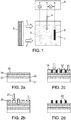
- an electrolysis bath 1 contains an aqueous solution containing one or more metal cations for the electrodeposition of metallic zinc as contact on the front face of a solar cell, for example based on CIGS in an embodiment presented below.
- the main metallic element deposited for contact is zinc (Zn °). It is deposited on a stack of a photovoltaic cell in thin layers (without contact) bearing the reference 2 playing the role of “working electrode”.
- Electrolysis reactor 1 contains a solution of zinc chloride (ZnCl 2 ) as a source of zinc, and possibly a background salt of potassium chloride (KCl) and possibly a leveling agent (for example boric acid H 3 BO 3 ).
- ZnCl 2 zinc chloride
- KCl potassium chloride
- leveling agent for example boric acid H 3 BO 3
- a counter-electrode 3 is also immersed in the bath. It 3 is composed of a noble metal (Ti, Pt). As a variant, it 3 is of the “sacrificial electrode” type, made of zinc, to ensure the renewal of the zinc ions in solution.
- the electrodeposition is preferably photo-assisted by lighting 7 from a light source 6.
- a saturated calomel electrode 4 (ECS: +245 mV / ENH) is used as a reference electrode.
- the deposition can be carried out by a potentiostatic technique (fixed reduction potential, applied by a voltage / current generator 5), or by an intentiostatic method (constant applied current density, fixed by the generator 5).
- intentiostatic deposition for example, the growth of the metallic contact is only controlled by the current applied between the substrate (working electrode) and the counter-electrode.
- the use of a reference electrode is then no longer necessary, allowing the implementation of an extremely simple method with two electrodes.
- the stack of the photovoltaic cell is initially deposited on a substrate 21 which may be a glass plate or a flexible polymer sheet of polyamide type covered with a thin metallic layer, or a metallic strip.
- the buffer layer 24 becomes an emitter layer, made of n-type or p-type silicon, respectively, and covering the p- or n-type silicon absorber.
- a mask 26 ( figure 2b ) on the surface of the window layer 25.
- This is an electrically insulating film, transparent in the visible range, for example a reusable plastic mask, an adhesive, a resin textured by photolithography or an anti-reflective layer textured by mechanical etching or laser.
- a luminous flux 27 is then applied opposite the stack to initiate the growth of the zinc by electrolysis.
- the stack reacts to this luminous flux 27 by generating a photo-current promoting the growth of the zinc layer in the parts (reference 28 of the figure 2c ) left free by the mask 26.
- the current generated under luminous flux over the entire surface of the substrate by the p / n junction is consumed by the reaction of reduction of the zinc ions to metallic zinc at the places left free by the mask .
- These areas form a grid pattern adapted to the chosen area of the cell.
- the mask 26 is an electrical insulator and thus prevents the zinc reduction reaction in the areas of the surface of the stack where the mask is present.
- a zinc metal contact pattern 28 with very good geometric definition is then obtained, after removal of the mask 26 ( figure 2d ).
- the figure 3 highlights the importance of the illumination for the electrodeposition on the type of substrate considered. Without illumination, very little current is recorded, involving little or no deposit. On the contrary, under illumination (phases (27)), a large current is recorded, meaning that the deposition is very fast. Typical speeds of the order of 3 microns / minute have thus been obtained.
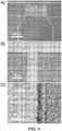
- the figure 4 shows the morphology of an electrodeposited zinc contact after removal of the mask. Observations with a scanning electron microscope show that the deposit is compact and finely respects the initial pattern, ensuring high definition of the contacts.
- the figure 5 shows examples of grids that can be deposited by electrodeposition.
- the deposit adapts well to any type of geometry.
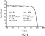
- the figure 6 compares the current-voltage characteristics of a solar cell with metal contact electroplated in zinc and evaporated in nickel-aluminum alloy in the case of a CIGS-based solar cell.
- the stacks were produced under the same conditions (in particular with electrodeposited ZnO to form the window layer).
- the photovoltaic efficiency of the solar cell with electroplated zinc contact is better than that of the cell with evaporated contact.
- Zinc on the other hand, is usually discarded because of its theoretical electrical properties which are inferior to those of copper and nickel. However, it turns out in reality that this is a candidate with very good performance, in particular for the solar panel industry. In addition, zinc is a very abundant and inexpensive material, about 2.5 times cheaper than copper for example.
- the absorber the buffer layer, the ZnO window layer, then the metal contacts.
- the solar cell is thus produced entirely (with the exception of the glass substrate and of the molybdenum layer for adaptation to the substrate) under atmospheric conditions (and advantageously, by electrolysis).
- an intermediate mask has been described above by way of exemplary embodiment.
- Other techniques can be provided, of course, such as, for example, the deposition of a solid layer, followed by etching.
- the description of the embodiment using a mask therefore aims to show here the perfect morphology of the deposit and its fineness, in particular in relation to the figures 4 and 5 .
Landscapes
- Photovoltaic Devices (AREA)
Claims (11)
- Verfahren zur Herstellung einer Dünnschicht-Photovoltaikzelle, wobei das Verfahren einen Schritt des Abscheidens mindestens eines Metallkontaktes (28) auf einer leitfähigen transparenten Schicht (25) eines Dünnschichtstapels beinhaltet, den die Zelle beinhaltet, dadurch gekennzeichnet, dass:- der Metallkontakt aus Zink ausgeführt ist,- die transparente Schicht aus Zinkoxid besteht,- der Schritt des Abscheidens durch Elektrolyse ausgeführt wird,- und die transparente Schicht durch Elektrolyse abgeschieden wird.
- Verfahren nach Anspruch 1, dadurch gekennzeichnet, dass der Schichtstapel eine Schicht mit photovoltaischen Eigenschaften beinhaltet, die mindestens mit der transparenten Schicht überzogen ist, auf welcher der Kontakt abgeschieden wird, wobei das Abscheiden durch Elektrolyse durch Beleuchten aus einer gegenüber dem Schichtstapel angeordneten Lichtquelle photounterstützt wird.
- Verfahren nach einem der vorhergehenden Ansprüche, dadurch gekennzeichnet, dass der Dünnschichtstapel eine Schicht mit photovoltaischen Eigenschaften beinhaltet auf der Basis von:- Kupfer,- Indium und/oder Gallium und- Selen und/oder Schwefel.
- Verfahren nach einem der vorhergehenden Ansprüche, bei dem der Stapel mindestens eine Absorberschicht mit photovoltaischen Eigenschaften beinhaltet und die Zelle ein auf dem Stapel abgeschiedenes Metallkontaktmuster beinhaltet,
dadurch gekennzeichnet, dass das Verfahren die folgenden Schritte umfasst:- Abscheiden einer elektrisch isolierenden Maske (26) auf dem Stapel, wobei die Maske diskontinuierlich ist, so dass Flächenbereiche des Stapels von der Maske frei gelassen werden, und- Abscheiden des Kontaktmusters auf den freien Flächenbereichen durch Elektrolyse,• wobei das Abscheiden des Kontaktmusters durch eine Lichtquelle photounterstützt wird, so dass die Absorberschicht durch photovoltaischen Effekt einen Photostrom erzeugt, der das Abscheiden durch Elektrolyse in den freien Flächenbereichen begünstigt, und• wobei die isolierende Maske außerhalb der freien Bereiche eine Barriere für den Photostrom bildet, die ein Abscheiden von Zink außerhalb der freien Bereiche verhindert. - Verfahren nach einem der vorhergehenden Ansprüche, dadurch gekennzeichnet, dass die Elektrolyse in einem Bad ausgeführt wird, das eine Zinkchloridlösung ZnCl2 enthält.
- Verfahren nach einem der vorhergehenden Ansprüche, dadurch gekennzeichnet, dass die Elektrolyse in einem Bad ausgeführt wird, in das eine Opferelektrode aus Zink getaucht wird.
- Verfahren nach einem der Ansprüche 5 und 6, dadurch gekennzeichnet, dass das Bad ferner ein Grundsalz aus Kaliumchlorid enthält.
- Verfahren nach einem der vorhergehenden Ansprüche, dadurch gekennzeichnet, dass die Elektrolyse in einem Bad ausgeführt wird, das neben einer Zinkquelle ein Nivelliermittel vom Typ Borsäure enthält.
- Verfahren nach einem der vorhergehenden Ansprüche, dadurch gekennzeichnet, dass das Abscheiden durch Elektrolyse bei konstantem Reduktionspotential ausgeführt wird.
- Verfahren nach einem der Ansprüche 1 bis 8, dadurch gekennzeichnet, dass das Abscheiden durch Elektrolyse bei angelegter konstanter Stromdichte ausgeführt wird.
- Photovoltaikzelle, die durch die Implementierung des Verfahrens nach einem der vorhergehenden Ansprüche erhalten wird und einen Dünnschichtstapel und mindestens einen Metallkontakt (28) beinhaltet, der auf einer leitfähigen transparenten Schicht (25) aus Zinkoxid abgeschieden ist, die der Stapel beinhaltet, dadurch gekennzeichnet, dass der Metallkontakt aus Zink ausgeführt ist.
Applications Claiming Priority (2)
| Application Number | Priority Date | Filing Date | Title |
|---|---|---|---|
| FR1554837A FR3036852B1 (fr) | 2015-05-28 | 2015-05-28 | Fabrication d'une cellule photovoltaique en couches minces a contacts metalliques perfectionnes |
| PCT/FR2016/051254 WO2016189258A1 (fr) | 2015-05-28 | 2016-05-26 | Fabrication d'une cellule photovoltaïque en couches minces à contacts métalliques perfectionnés |
Publications (2)
| Publication Number | Publication Date |
|---|---|
| EP3304603A1 EP3304603A1 (de) | 2018-04-11 |
| EP3304603B1 true EP3304603B1 (de) | 2020-07-29 |
Family
ID=54199785
Family Applications (1)
| Application Number | Title | Priority Date | Filing Date |
|---|---|---|---|
| EP16729322.4A Active EP3304603B1 (de) | 2015-05-28 | 2016-05-26 | Herstellung einer fotovoltaischen dünnschichtzelle mit fortschrittlichen metallkontakten |
Country Status (3)
| Country | Link |
|---|---|
| EP (1) | EP3304603B1 (de) |
| FR (1) | FR3036852B1 (de) |
| WO (1) | WO2016189258A1 (de) |
Family Cites Families (5)
| Publication number | Priority date | Publication date | Assignee | Title |
|---|---|---|---|---|
| US20080035489A1 (en) * | 2006-06-05 | 2008-02-14 | Rohm And Haas Electronic Materials Llc | Plating process |
| US20080128019A1 (en) * | 2006-12-01 | 2008-06-05 | Applied Materials, Inc. | Method of metallizing a solar cell substrate |
| US20110253545A1 (en) * | 2010-04-19 | 2011-10-20 | International Business Machines Corporation | Method of direct electrodeposition on semiconductors |
| WO2012127397A1 (en) * | 2011-03-18 | 2012-09-27 | Somont Gmbh | Methods and system for producing atleast a photovoltaic device with atleast a protective member |
| US9634176B2 (en) * | 2013-05-29 | 2017-04-25 | Kaneka Corporation | Method for manufacturing crystalline silicon-based solar cell and method for manufacturing crystalline silicon-based solar cell module |
-
2015
- 2015-05-28 FR FR1554837A patent/FR3036852B1/fr active Active
-
2016
- 2016-05-26 WO PCT/FR2016/051254 patent/WO2016189258A1/fr not_active Ceased
- 2016-05-26 EP EP16729322.4A patent/EP3304603B1/de active Active
Non-Patent Citations (1)
| Title |
|---|
| None * |
Also Published As
| Publication number | Publication date |
|---|---|
| FR3036852A1 (fr) | 2016-12-02 |
| WO2016189258A1 (fr) | 2016-12-01 |
| EP3304603A1 (de) | 2018-04-11 |
| FR3036852B1 (fr) | 2017-06-16 |
Similar Documents
| Publication | Publication Date | Title |
|---|---|---|
| EP2381486B1 (de) | Verfahren zur Herstellung der Rückkontaktelektroden für Cadmiumtellurid-Photovoltaikzellen | |
| US8829342B2 (en) | Back contact buffer layer for thin-film solar cells | |
| EP2777075B1 (de) | Leitendes substrat für photovoltaische zelle | |
| FR2985606A1 (fr) | Procede pour realiser un module photovoltaique avec deux etapes de gravure p2 et p3 et module photovoltaique correspondant. | |
| EP2318572B1 (de) | Bildung eines transparenten leitfähigen oxidfilms zur verwendung in einer photovoltaikstruktur | |
| KR20120087030A (ko) | 태양광 발전장치 및 제조방법 | |
| EP2803088A1 (de) | Verfahren zur herstellung eines pv-moduls mit zwei ätzschritten p1 und p3 sowie entsprechendes pv-modul | |
| EP3523828B1 (de) | Verbesserte kontakte für eine fotovoltaische zelle mit zwei aktiven flächen | |
| EP3304603B1 (de) | Herstellung einer fotovoltaischen dünnschichtzelle mit fortschrittlichen metallkontakten | |
| EP2834848A1 (de) | Verfahren zur herstellung eines fotovoltaikmoduls mit einem ätzschritt p3 und einem optionalen schritt p1 | |
| EP3776665B1 (de) | Optimierung des elektrischen metall/metall-kontakts in einer semitransparenten fotovoltaischen dünnschichtvorrichtung | |
| WO2012143632A1 (fr) | Integration d'une couche 2d cristalline a base de zno sur un substrat plastique conducteur | |
| US20140060608A1 (en) | Photovoltaic device and method of making | |
| FR3018392A1 (fr) | Module solaire photovoltaique semi-transparent en couches minces et son procede de fabrication | |
| FR3031240A3 (fr) | Substrat conducteur pour cellule photovoltaique | |
| EP3069386B1 (de) | Rückkontaktsubstrat für eine photovoltaische zelle | |
| FR2989224A1 (fr) | Procede pour realiser un module photovoltaique avec une etape de gravure p3 et une eventuelle etape p2. | |
| Golan et al. | Properties investigation of thin films photovoltaic hetero-structures | |
| EP3005425B1 (de) | Verfahren zur herstellung des p-n-übergangs einer fotovoltaischen dünnschichtzelle und zugehöriges verfahren zur herstellung einer fotovoltaischen zelle | |
| FR2955428A1 (fr) | Fabrication d'une structure multicouche pour des applications photovoltaiques a partir de conditions d'electrolyse perfectionnees. | |
| KR20120086202A (ko) | 태양광 발전장치 및 이의 제조방법 |
Legal Events
| Date | Code | Title | Description |
|---|---|---|---|
| STAA | Information on the status of an ep patent application or granted ep patent |
Free format text: STATUS: THE INTERNATIONAL PUBLICATION HAS BEEN MADE |
|
| PUAI | Public reference made under article 153(3) epc to a published international application that has entered the european phase |
Free format text: ORIGINAL CODE: 0009012 |
|
| STAA | Information on the status of an ep patent application or granted ep patent |
Free format text: STATUS: REQUEST FOR EXAMINATION WAS MADE |
|
| 17P | Request for examination filed |
Effective date: 20171122 |
|
| AK | Designated contracting states |
Kind code of ref document: A1 Designated state(s): AL AT BE BG CH CY CZ DE DK EE ES FI FR GB GR HR HU IE IS IT LI LT LU LV MC MK MT NL NO PL PT RO RS SE SI SK SM TR |
|
| AX | Request for extension of the european patent |
Extension state: BA ME |
|
| DAV | Request for validation of the european patent (deleted) | ||
| DAX | Request for extension of the european patent (deleted) | ||
| STAA | Information on the status of an ep patent application or granted ep patent |
Free format text: STATUS: EXAMINATION IS IN PROGRESS |
|
| 17Q | First examination report despatched |
Effective date: 20190703 |
|
| GRAP | Despatch of communication of intention to grant a patent |
Free format text: ORIGINAL CODE: EPIDOSNIGR1 |
|
| STAA | Information on the status of an ep patent application or granted ep patent |
Free format text: STATUS: GRANT OF PATENT IS INTENDED |
|
| INTG | Intention to grant announced |
Effective date: 20200309 |
|
| GRAS | Grant fee paid |
Free format text: ORIGINAL CODE: EPIDOSNIGR3 |
|
| GRAA | (expected) grant |
Free format text: ORIGINAL CODE: 0009210 |
|
| STAA | Information on the status of an ep patent application or granted ep patent |
Free format text: STATUS: THE PATENT HAS BEEN GRANTED |
|
| AK | Designated contracting states |
Kind code of ref document: B1 Designated state(s): AL AT BE BG CH CY CZ DE DK EE ES FI FR GB GR HR HU IE IS IT LI LT LU LV MC MK MT NL NO PL PT RO RS SE SI SK SM TR |
|
| REG | Reference to a national code |
Ref country code: CH Ref legal event code: EP |
|
| REG | Reference to a national code |
Ref country code: AT Ref legal event code: REF Ref document number: 1296813 Country of ref document: AT Kind code of ref document: T Effective date: 20200815 |
|
| REG | Reference to a national code |
Ref country code: IE Ref legal event code: FG4D Free format text: LANGUAGE OF EP DOCUMENT: FRENCH |
|
| REG | Reference to a national code |
Ref country code: DE Ref legal event code: R096 Ref document number: 602016040816 Country of ref document: DE |
|
| REG | Reference to a national code |
Ref country code: LT Ref legal event code: MG4D |
|
| REG | Reference to a national code |
Ref country code: NL Ref legal event code: MP Effective date: 20200729 |
|
| REG | Reference to a national code |
Ref country code: AT Ref legal event code: MK05 Ref document number: 1296813 Country of ref document: AT Kind code of ref document: T Effective date: 20200729 |
|
| PG25 | Lapsed in a contracting state [announced via postgrant information from national office to epo] |
Ref country code: ES Free format text: LAPSE BECAUSE OF FAILURE TO SUBMIT A TRANSLATION OF THE DESCRIPTION OR TO PAY THE FEE WITHIN THE PRESCRIBED TIME-LIMIT Effective date: 20200729 Ref country code: SE Free format text: LAPSE BECAUSE OF FAILURE TO SUBMIT A TRANSLATION OF THE DESCRIPTION OR TO PAY THE FEE WITHIN THE PRESCRIBED TIME-LIMIT Effective date: 20200729 Ref country code: BG Free format text: LAPSE BECAUSE OF FAILURE TO SUBMIT A TRANSLATION OF THE DESCRIPTION OR TO PAY THE FEE WITHIN THE PRESCRIBED TIME-LIMIT Effective date: 20201029 Ref country code: AT Free format text: LAPSE BECAUSE OF FAILURE TO SUBMIT A TRANSLATION OF THE DESCRIPTION OR TO PAY THE FEE WITHIN THE PRESCRIBED TIME-LIMIT Effective date: 20200729 Ref country code: NO Free format text: LAPSE BECAUSE OF FAILURE TO SUBMIT A TRANSLATION OF THE DESCRIPTION OR TO PAY THE FEE WITHIN THE PRESCRIBED TIME-LIMIT Effective date: 20201029 Ref country code: GR Free format text: LAPSE BECAUSE OF FAILURE TO SUBMIT A TRANSLATION OF THE DESCRIPTION OR TO PAY THE FEE WITHIN THE PRESCRIBED TIME-LIMIT Effective date: 20201030 Ref country code: FI Free format text: LAPSE BECAUSE OF FAILURE TO SUBMIT A TRANSLATION OF THE DESCRIPTION OR TO PAY THE FEE WITHIN THE PRESCRIBED TIME-LIMIT Effective date: 20200729 Ref country code: PT Free format text: LAPSE BECAUSE OF FAILURE TO SUBMIT A TRANSLATION OF THE DESCRIPTION OR TO PAY THE FEE WITHIN THE PRESCRIBED TIME-LIMIT Effective date: 20201130 Ref country code: HR Free format text: LAPSE BECAUSE OF FAILURE TO SUBMIT A TRANSLATION OF THE DESCRIPTION OR TO PAY THE FEE WITHIN THE PRESCRIBED TIME-LIMIT Effective date: 20200729 Ref country code: LT Free format text: LAPSE BECAUSE OF FAILURE TO SUBMIT A TRANSLATION OF THE DESCRIPTION OR TO PAY THE FEE WITHIN THE PRESCRIBED TIME-LIMIT Effective date: 20200729 |
|
| PG25 | Lapsed in a contracting state [announced via postgrant information from national office to epo] |
Ref country code: LV Free format text: LAPSE BECAUSE OF FAILURE TO SUBMIT A TRANSLATION OF THE DESCRIPTION OR TO PAY THE FEE WITHIN THE PRESCRIBED TIME-LIMIT Effective date: 20200729 Ref country code: PL Free format text: LAPSE BECAUSE OF FAILURE TO SUBMIT A TRANSLATION OF THE DESCRIPTION OR TO PAY THE FEE WITHIN THE PRESCRIBED TIME-LIMIT Effective date: 20200729 Ref country code: RS Free format text: LAPSE BECAUSE OF FAILURE TO SUBMIT A TRANSLATION OF THE DESCRIPTION OR TO PAY THE FEE WITHIN THE PRESCRIBED TIME-LIMIT Effective date: 20200729 Ref country code: IS Free format text: LAPSE BECAUSE OF FAILURE TO SUBMIT A TRANSLATION OF THE DESCRIPTION OR TO PAY THE FEE WITHIN THE PRESCRIBED TIME-LIMIT Effective date: 20201129 |
|
| PG25 | Lapsed in a contracting state [announced via postgrant information from national office to epo] |
Ref country code: NL Free format text: LAPSE BECAUSE OF FAILURE TO SUBMIT A TRANSLATION OF THE DESCRIPTION OR TO PAY THE FEE WITHIN THE PRESCRIBED TIME-LIMIT Effective date: 20200729 |
|
| PG25 | Lapsed in a contracting state [announced via postgrant information from national office to epo] |
Ref country code: IT Free format text: LAPSE BECAUSE OF FAILURE TO SUBMIT A TRANSLATION OF THE DESCRIPTION OR TO PAY THE FEE WITHIN THE PRESCRIBED TIME-LIMIT Effective date: 20200729 Ref country code: EE Free format text: LAPSE BECAUSE OF FAILURE TO SUBMIT A TRANSLATION OF THE DESCRIPTION OR TO PAY THE FEE WITHIN THE PRESCRIBED TIME-LIMIT Effective date: 20200729 Ref country code: CZ Free format text: LAPSE BECAUSE OF FAILURE TO SUBMIT A TRANSLATION OF THE DESCRIPTION OR TO PAY THE FEE WITHIN THE PRESCRIBED TIME-LIMIT Effective date: 20200729 Ref country code: DK Free format text: LAPSE BECAUSE OF FAILURE TO SUBMIT A TRANSLATION OF THE DESCRIPTION OR TO PAY THE FEE WITHIN THE PRESCRIBED TIME-LIMIT Effective date: 20200729 Ref country code: SM Free format text: LAPSE BECAUSE OF FAILURE TO SUBMIT A TRANSLATION OF THE DESCRIPTION OR TO PAY THE FEE WITHIN THE PRESCRIBED TIME-LIMIT Effective date: 20200729 Ref country code: RO Free format text: LAPSE BECAUSE OF FAILURE TO SUBMIT A TRANSLATION OF THE DESCRIPTION OR TO PAY THE FEE WITHIN THE PRESCRIBED TIME-LIMIT Effective date: 20200729 |
|
| REG | Reference to a national code |
Ref country code: DE Ref legal event code: R097 Ref document number: 602016040816 Country of ref document: DE |
|
| PG25 | Lapsed in a contracting state [announced via postgrant information from national office to epo] |
Ref country code: AL Free format text: LAPSE BECAUSE OF FAILURE TO SUBMIT A TRANSLATION OF THE DESCRIPTION OR TO PAY THE FEE WITHIN THE PRESCRIBED TIME-LIMIT Effective date: 20200729 |
|
| PLBE | No opposition filed within time limit |
Free format text: ORIGINAL CODE: 0009261 |
|
| STAA | Information on the status of an ep patent application or granted ep patent |
Free format text: STATUS: NO OPPOSITION FILED WITHIN TIME LIMIT |
|
| PG25 | Lapsed in a contracting state [announced via postgrant information from national office to epo] |
Ref country code: SK Free format text: LAPSE BECAUSE OF FAILURE TO SUBMIT A TRANSLATION OF THE DESCRIPTION OR TO PAY THE FEE WITHIN THE PRESCRIBED TIME-LIMIT Effective date: 20200729 |
|
| 26N | No opposition filed |
Effective date: 20210430 |
|
| PG25 | Lapsed in a contracting state [announced via postgrant information from national office to epo] |
Ref country code: SI Free format text: LAPSE BECAUSE OF FAILURE TO SUBMIT A TRANSLATION OF THE DESCRIPTION OR TO PAY THE FEE WITHIN THE PRESCRIBED TIME-LIMIT Effective date: 20200729 |
|
| REG | Reference to a national code |
Ref country code: CH Ref legal event code: PL |
|
| GBPC | Gb: european patent ceased through non-payment of renewal fee |
Effective date: 20210526 |
|
| PG25 | Lapsed in a contracting state [announced via postgrant information from national office to epo] |
Ref country code: CH Free format text: LAPSE BECAUSE OF NON-PAYMENT OF DUE FEES Effective date: 20210531 Ref country code: MC Free format text: LAPSE BECAUSE OF FAILURE TO SUBMIT A TRANSLATION OF THE DESCRIPTION OR TO PAY THE FEE WITHIN THE PRESCRIBED TIME-LIMIT Effective date: 20200729 Ref country code: LI Free format text: LAPSE BECAUSE OF NON-PAYMENT OF DUE FEES Effective date: 20210531 Ref country code: LU Free format text: LAPSE BECAUSE OF NON-PAYMENT OF DUE FEES Effective date: 20210526 |
|
| REG | Reference to a national code |
Ref country code: BE Ref legal event code: MM Effective date: 20210531 |
|
| PG25 | Lapsed in a contracting state [announced via postgrant information from national office to epo] |
Ref country code: IE Free format text: LAPSE BECAUSE OF NON-PAYMENT OF DUE FEES Effective date: 20210526 Ref country code: GB Free format text: LAPSE BECAUSE OF NON-PAYMENT OF DUE FEES Effective date: 20210526 |
|
| PG25 | Lapsed in a contracting state [announced via postgrant information from national office to epo] |
Ref country code: BE Free format text: LAPSE BECAUSE OF NON-PAYMENT OF DUE FEES Effective date: 20210531 |
|
| PG25 | Lapsed in a contracting state [announced via postgrant information from national office to epo] |
Ref country code: CY Free format text: LAPSE BECAUSE OF FAILURE TO SUBMIT A TRANSLATION OF THE DESCRIPTION OR TO PAY THE FEE WITHIN THE PRESCRIBED TIME-LIMIT Effective date: 20200729 |
|
| PG25 | Lapsed in a contracting state [announced via postgrant information from national office to epo] |
Ref country code: HU Free format text: LAPSE BECAUSE OF FAILURE TO SUBMIT A TRANSLATION OF THE DESCRIPTION OR TO PAY THE FEE WITHIN THE PRESCRIBED TIME-LIMIT; INVALID AB INITIO Effective date: 20160526 |
|
| PG25 | Lapsed in a contracting state [announced via postgrant information from national office to epo] |
Ref country code: MK Free format text: LAPSE BECAUSE OF FAILURE TO SUBMIT A TRANSLATION OF THE DESCRIPTION OR TO PAY THE FEE WITHIN THE PRESCRIBED TIME-LIMIT Effective date: 20200729 |
|
| PG25 | Lapsed in a contracting state [announced via postgrant information from national office to epo] |
Ref country code: MT Free format text: LAPSE BECAUSE OF FAILURE TO SUBMIT A TRANSLATION OF THE DESCRIPTION OR TO PAY THE FEE WITHIN THE PRESCRIBED TIME-LIMIT Effective date: 20200729 |
|
| REG | Reference to a national code |
Ref country code: DE Ref legal event code: R079 Ref document number: 602016040816 Country of ref document: DE Free format text: PREVIOUS MAIN CLASS: H01L0031022400 Ipc: H10F0077200000 |
|
| PGFP | Annual fee paid to national office [announced via postgrant information from national office to epo] |
Ref country code: DE Payment date: 20250513 Year of fee payment: 10 |
|
| PGFP | Annual fee paid to national office [announced via postgrant information from national office to epo] |
Ref country code: FR Payment date: 20250422 Year of fee payment: 10 |
|
| PG25 | Lapsed in a contracting state [announced via postgrant information from national office to epo] |
Ref country code: TR Free format text: LAPSE BECAUSE OF FAILURE TO SUBMIT A TRANSLATION OF THE DESCRIPTION OR TO PAY THE FEE WITHIN THE PRESCRIBED TIME-LIMIT Effective date: 20200729 |