EP3304613B1 - Écrans flexibles ayant des couches rigides pour un ajustage de plan neutre - Google Patents
Écrans flexibles ayant des couches rigides pour un ajustage de plan neutre Download PDFInfo
- Publication number
- EP3304613B1 EP3304613B1 EP16730564.8A EP16730564A EP3304613B1 EP 3304613 B1 EP3304613 B1 EP 3304613B1 EP 16730564 A EP16730564 A EP 16730564A EP 3304613 B1 EP3304613 B1 EP 3304613B1
- Authority
- EP
- European Patent Office
- Prior art keywords
- layer
- interlocking
- display
- stiff
- flexible display
- Prior art date
- Legal status (The legal status is an assumption and is not a legal conclusion. Google has not performed a legal analysis and makes no representation as to the accuracy of the status listed.)
- Not-in-force
Links
Images


Classifications
-
- H—ELECTRICITY
- H10—SEMICONDUCTOR DEVICES; ELECTRIC SOLID-STATE DEVICES NOT OTHERWISE PROVIDED FOR
- H10K—ORGANIC ELECTRIC SOLID-STATE DEVICES
- H10K77/00—Constructional details of devices covered by this subclass and not covered by groups H10K10/80, H10K30/80, H10K50/80 or H10K59/80
- H10K77/10—Substrates, e.g. flexible substrates
- H10K77/111—Flexible substrates
-
- H—ELECTRICITY
- H10—SEMICONDUCTOR DEVICES; ELECTRIC SOLID-STATE DEVICES NOT OTHERWISE PROVIDED FOR
- H10K—ORGANIC ELECTRIC SOLID-STATE DEVICES
- H10K59/00—Integrated devices, or assemblies of multiple devices, comprising at least one organic light-emitting element covered by group H10K50/00
- H10K59/80—Constructional details
- H10K59/87—Passivation; Containers; Encapsulations
- H10K59/871—Self-supporting sealing arrangements
-
- F—MECHANICAL ENGINEERING; LIGHTING; HEATING; WEAPONS; BLASTING
- F21—LIGHTING
- F21K—NON-ELECTRIC LIGHT SOURCES USING LUMINESCENCE; LIGHT SOURCES USING ELECTROCHEMILUMINESCENCE; LIGHT SOURCES USING CHARGES OF COMBUSTIBLE MATERIAL; LIGHT SOURCES USING SEMICONDUCTOR DEVICES AS LIGHT-GENERATING ELEMENTS; LIGHT SOURCES NOT OTHERWISE PROVIDED FOR
- F21K9/00—Light sources using semiconductor devices as light-generating elements, e.g. using light-emitting diodes [LED] or lasers
- F21K9/60—Optical arrangements integrated in the light source, e.g. for improving the colour rendering index or the light extraction
- F21K9/69—Details of refractors forming part of the light source
-
- G—PHYSICS
- G09—EDUCATION; CRYPTOGRAPHY; DISPLAY; ADVERTISING; SEALS
- G09F—DISPLAYING; ADVERTISING; SIGNS; LABELS OR NAME-PLATES; SEALS
- G09F9/00—Indicating arrangements for variable information in which the information is built-up on a support by selection or combination of individual elements
- G09F9/30—Indicating arrangements for variable information in which the information is built-up on a support by selection or combination of individual elements in which the desired character or characters are formed by combining individual elements
- G09F9/301—Indicating arrangements for variable information in which the information is built-up on a support by selection or combination of individual elements in which the desired character or characters are formed by combining individual elements flexible foldable or roll-able electronic displays, e.g. thin LCD, OLED
-
- H—ELECTRICITY
- H05—ELECTRIC TECHNIQUES NOT OTHERWISE PROVIDED FOR
- H05K—PRINTED CIRCUITS; CASINGS OR CONSTRUCTIONAL DETAILS OF ELECTRIC APPARATUS; MANUFACTURE OF ASSEMBLAGES OF ELECTRICAL COMPONENTS
- H05K1/00—Printed circuits
- H05K1/02—Details
- H05K1/0277—Bendability or stretchability details
- H05K1/028—Bending or folding regions of flexible printed circuits
- H05K1/0281—Reinforcement details thereof
-
- H—ELECTRICITY
- H05—ELECTRIC TECHNIQUES NOT OTHERWISE PROVIDED FOR
- H05K—PRINTED CIRCUITS; CASINGS OR CONSTRUCTIONAL DETAILS OF ELECTRIC APPARATUS; MANUFACTURE OF ASSEMBLAGES OF ELECTRICAL COMPONENTS
- H05K5/00—Casings, cabinets or drawers for electric apparatus
- H05K5/02—Details
- H05K5/0217—Mechanical details of casings
- H05K5/0221—Locks; Latches
-
- H—ELECTRICITY
- H10—SEMICONDUCTOR DEVICES; ELECTRIC SOLID-STATE DEVICES NOT OTHERWISE PROVIDED FOR
- H10K—ORGANIC ELECTRIC SOLID-STATE DEVICES
- H10K50/00—Organic light-emitting devices
- H10K50/80—Constructional details
- H10K50/84—Passivation; Containers; Encapsulations
- H10K50/841—Self-supporting sealing arrangements
-
- H—ELECTRICITY
- H10—SEMICONDUCTOR DEVICES; ELECTRIC SOLID-STATE DEVICES NOT OTHERWISE PROVIDED FOR
- H10K—ORGANIC ELECTRIC SOLID-STATE DEVICES
- H10K50/00—Organic light-emitting devices
- H10K50/80—Constructional details
- H10K50/84—Passivation; Containers; Encapsulations
- H10K50/842—Containers
- H10K50/8426—Peripheral sealing arrangements, e.g. adhesives, sealants
-
- H—ELECTRICITY
- H10—SEMICONDUCTOR DEVICES; ELECTRIC SOLID-STATE DEVICES NOT OTHERWISE PROVIDED FOR
- H10K—ORGANIC ELECTRIC SOLID-STATE DEVICES
- H10K59/00—Integrated devices, or assemblies of multiple devices, comprising at least one organic light-emitting element covered by group H10K50/00
- H10K59/10—OLED displays
-
- H—ELECTRICITY
- H10—SEMICONDUCTOR DEVICES; ELECTRIC SOLID-STATE DEVICES NOT OTHERWISE PROVIDED FOR
- H10K—ORGANIC ELECTRIC SOLID-STATE DEVICES
- H10K59/00—Integrated devices, or assemblies of multiple devices, comprising at least one organic light-emitting element covered by group H10K50/00
- H10K59/80—Constructional details
- H10K59/87—Passivation; Containers; Encapsulations
- H10K59/871—Self-supporting sealing arrangements
- H10K59/8722—Peripheral sealing arrangements, e.g. adhesives, sealants
-
- H—ELECTRICITY
- H10—SEMICONDUCTOR DEVICES; ELECTRIC SOLID-STATE DEVICES NOT OTHERWISE PROVIDED FOR
- H10K—ORGANIC ELECTRIC SOLID-STATE DEVICES
- H10K2102/00—Constructional details relating to the organic devices covered by this subclass
- H10K2102/301—Details of OLEDs
- H10K2102/311—Flexible OLED
-
- Y—GENERAL TAGGING OF NEW TECHNOLOGICAL DEVELOPMENTS; GENERAL TAGGING OF CROSS-SECTIONAL TECHNOLOGIES SPANNING OVER SEVERAL SECTIONS OF THE IPC; TECHNICAL SUBJECTS COVERED BY FORMER USPC CROSS-REFERENCE ART COLLECTIONS [XRACs] AND DIGESTS
- Y02—TECHNOLOGIES OR APPLICATIONS FOR MITIGATION OR ADAPTATION AGAINST CLIMATE CHANGE
- Y02E—REDUCTION OF GREENHOUSE GAS [GHG] EMISSIONS, RELATED TO ENERGY GENERATION, TRANSMISSION OR DISTRIBUTION
- Y02E10/00—Energy generation through renewable energy sources
- Y02E10/50—Photovoltaic [PV] energy
- Y02E10/549—Organic PV cells
Definitions
- At least some aspects of the present disclosure relate to displays with interlocking devices. At least some aspects of the present disclosure relate to displays having stiff layers for neutral plane adjustment.
- US 2010/0258346 A1 discloses a package of an environmentally sensitive electronic device including a first substrate, a second substrate, an environmentally sensitive electronic device, a plurality of barrier structures, and a fill.
- a flexible display comprising: a plurality of functional layers comprising a display layer having a display component, a plurality of bonding layers comprising a bonding component, and a stiff layer.
- a plurality of bonding layers comprising a display layer having a display component
- a plurality of bonding layers comprising a bonding component
- a stiff layer Each of the plurality of bonding layers is disposed between two adjacent functional layers.
- the stiff layer having an elastic modulus greater than an elastic modulus of each of the plurality of functional layers to adjust a position of a neutral plane of the flexible display within the display layer.
- spatially related terms including but not limited to, “lower,” “upper,” “beneath,” “below,” “above,” and “on top,” if used herein, are utilized for ease of description to describe spatial relationships of an element(s) to another.
- Such spatially related terms encompass different orientations of the device in use or operation in addition to the particular orientations depicted in the figures and described herein. For example, if an object depicted in the figures is turned over or flipped over, portions previously described as below or beneath other elements would then be above those other elements.
- an element, component or layer for example when an element, component or layer for example is described as forming a "coincident interface" with, or being “on” “connected to,” “coupled to” or “in contact with” another element, component or layer, it can be directly on, directly connected to, directly coupled with, in direct contact with, or intervening elements, components or layers may be on, connected, coupled or in contact with the particular element, component or layer, for example.
- an element, component or layer for example is referred to as being “directly on,” “directly connected to,” “directly coupled to,” or “directly in contact with” another element, there are no intervening elements, components or layers for example.
- “powered” means a device receiving operational power.
- the interlocking device can be disposed between adjacent functional layers of a flexible display, for example, a support layer, a display layer, a protection layer, a touch device, or the like.
- Each functional layer can include one or more components.
- the display layer can include an organic light-emitting device or other display device.
- the protection layer can include a touch sensitive device, a protection film, a light enhancement film, or the like.
- the support layer can include a supporting substrate, batteries, electrical circuit layer, or the like.
- the interlocking device can be used with optical clear gel, adhesive, or liquid to improve bonding property and/or optical property.
- a neutral plane refers to a conceptual plane within a structure subjected to bending, where it is not under stress, neither compression nor tension.
- a stiff layer refers to a layer having a relative high elastic modulus, for example, greater than at least one layer or greater than other layers in a display. It is often desirable to position the neutral plane at, within, or proximate to the display layer where the display components are disposed.
- Figure 1 illustrates a close-up conceptual view of a portion of a display 100 using an interlocking device 110.
- the display 100 includes a first layer 120 and a second layer 130 and a bonding layer 150 disposed between the two layers (120, 130).
- the bonding layer 150 includes the interlocking device 110.
- the display may include other layers besides layers 120 and 130.
- the interlocking device 110 includes a first interlocking component 102 attached to or integrated with the layer 120 and a second interlocking component 104 attached to or integrated with the layer 130.
- the second interlocking component 104 is configured to engage with the first interlocking component 102.
- the engagement prevents the separation of the first layer 120 from the second layer 130 along the direction Z perpendicular to the surface of the second layer.
- the engagement between the first and second interlocking components provides little or no restriction of the first layer 120 sliding with respect to the second layer in the direction X along the surface of the second layer 130.
- the first interlocking component 120 and/or the second interlocking component 130 have channels that can facilitate or guide sliding between the two components.
- the first interlocking component 120 and/or the second interlocking component 130 have rails or generally aligned elements forming channels.
- the interlocking device 110 can use materials that are optically clear, for example, material with visible light transmission at least 90% and haze less than 2%. In some cases, the interlocking device 110 can be disposed outside viewing area. In such cases, the interlocking device 110 can use materials that are not optically clear. In some implementations, the interlocking device 110 can include air gap between interlocking components. In some other cases, at least part of the interlocking device 110 can be disposed within viewing area. In such cases, the part of the interlocking device 110 disposed in the viewing area using an optically clear material, for example, optically clear polymer, or the like.
- an optically clear material for example, optically clear polymer, or the like.
- the optically clear polymer may be a selected polymer with a refractive index between 1.50 and 1.60, for example, polyester, polymethylmethacrylate, polycarbonate, cyclic olefin copolymer, or the like.
- the bonding layer 150 can include bonding materials 140 can be disposed proximate to the first layer 120 and the second layer 130 together with the interlocking device 110.
- the bonding material 140 can include an optically clear material, for example, optically clear adhesive, optically clear gel, optically clear liquid, or the like.
- the bonding material 140 can use materials that have relative low viscosity, for example, a low viscosity liquid, to reduce resistance to bending.
- the bonding material 140 can use a material that has a refractive index closely matching the refractive index of the interlocking device 110.
- the bonding material 140 can have an overall refractive index that has an absolute difference less than or equal to 0.05 from the refractive index of the part of interlocking device 110, more particularly the interlocking components 102 and 104, within the viewing area.
- the bonding material 140 can include materials, for example, acrylates, urethanes, silicones, polyolefins, or the like.
- the interlocking device 110 has a height no more than 10 mm. In some cases, the interlocking device 110 has a height no more than 1 mm. In some cases, the interlocking device 110 has a height no more than 200 micrometers. In some cases, the interlocking device 110 has a height no more than 100 micrometers. In some cases, the interlocking device 110 has a height no less than 5 micrometers.
- the interlocking device 110 comprises an optical coupler 106 disposed proximate to the first interlocking component 102 and the second interlocking component 104.
- the optical coupler 106 includes materials that have relatively low elastic modulus, low creep, and a high degree of shear strain under shear load to facilitate the repeated bending, for example, liquid, adhesive, gel, or the like.
- the optical coupler 106 can include a low viscosity liquid to reduce frictional drag between interlocking components and reduce resistance to bending.
- the optical coupler 106 uses a material that has a refractive index closely matching the refractive index of the interlocking device 110, more particular the interlocking components 102 and 104. In such cases, the optical clarity of the interlocking device 110 can be restored by eliminating the air gaps between the interlocking components 102 and 104.
- the optical coupler 106 has an overall refractive index that has an absolute difference less than or equal to 0.05 from the refractive index of the part of interlocking device 110, more particularly the interlocking components 102 and 104, within the viewing area.
- the optical coupler 106 can include materials such as, for example liquids containing phenyl and phosphorus groups such as Santicizer 141 (available from Ferro, USA), or gels formulated using such liquids in combination with acrylate polymers using monomers containing higher refractive index contributing functional groups such as aromatic groups like phenyl, naphtyl, anthracyl, sulfur groups, bromine groups, or the like, to control and adjust the optical index of the gel. If a closely matching adhesive is used as optical coupling element 106 it cannot restrict the relative movement (i.e. relative sliding) of the interlocking device 110. In some cases, the optical coupler 106 can use the same material as the bonding material 140.
- the first interlocking component 102 or the second interlocking component 104 comprises a plurality of engagement elements. At least some of the engagement elements have a cross-sectional shape having a stem and a cap wider than the stem, as illustrated in Figure 1 , such that the engagement between the engagement elements prevents separation or displacement along the Z axis.
- the first or the second interlocking component includes a plurality of engagement rails allowing sliding along the X axis.
- at least some of the engagement rails has a cross-sectional shape having a post and a cap.
- each of the plurality of engagement elements or engagement rails has a height no more than 10 mm.
- each of the plurality of engagement elements or engagement rails has a height no more than 1 mm. In some cases, each of the plurality of engagement elements or engagement rails has a height no more than 200 micrometers. In some cases, each of the plurality of engagement elements or engagement rails has a height no more than 100 micrometers. In some cases, each of the plurality of engagement elements or engagement rails has a height no less than 5 micrometers.
- the first interlocking component 102 includes a set of first engagement elements and the second interlocking component 104 includes a set of second engagement elements.
- the first engagement elements have generally same shapes as the second engagement elements.
- the flexible display 100 has an X axis and a Y axis generally perpendicular to the X axis, where the flexible display 100 is configured to bend about the Y axis.
- the interlocking device 110 is disposed along the X axis. In some cases, the interlocking device 110 is disposed proximate to two opposing edges of the flexible display 100 along the X axis.
- the flexible display 100 may include more than two functional layers, where every two adjacent functional layers have a bonding layer in between and the bonding layer includes an interlocking device.
- an interlocking device 200A includes a first interlocking component 210A and a second interlocking component 220A configured to engage with the first interlocking component 210A.
- the first interlocking component 210A can include a substrate 211 and one or more engagement rails 215A.
- the second interlocking component 220A can include a substrate 221 and one or more engagement rails 225A.
- the engagement rail 215A includes a stem 212 and a cap 214A that is wider than the stem 212.
- the cross section of the engagement rail 215A is in a mushroom-like shape.
- the engagement rail 225A includes a stem 222 and a cap 224A that is wider than the stem 222. This design may have a little gap between the two interlocking components.
- Figure 2B illustrates a similar design of an interlocking device 200B as the interlocking device 200A.
- the first interlocking component 210B can include a substrate 211 and one or more engagement rails 215B.
- the second interlocking component 220B can include a substrate 221 and one or more engagement rails 225B.
- the engagement rail 215B includes a stem 212 and a cap 214B that is wider than the stem 212.
- the cross section of the engagement rail 215B is in a mushroom-like shape.
- the engagement rail 225B includes a stem 222 and a cap 224B that is wider than the stem 222.
- the two interlocking components (210B, 220B) have more overlaps between the caps (214B, 224B) that may provide higher through thickness bonding strength than the configuration illustrated in Figure 2A .
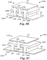
- FIG. 2C illustrates an example of an interlocking device 200C.
- the interlocking device 200C includes a first interlocking component 210C and a second interlocking component 220C configured to engage with the first interlocking component 210C.
- the first interlocking component 210C can include a substrate 211 and one or more engagement rails 215C.
- the second interlocking component 220C can include a substrate 221 and one or more engagement rails 225C.
- the engagement rail 215C includes a stem 212 and a cap 214C that is wider than the stem 212.
- the cross section of the engagement rail 215C is in a mushroom-like shape.
- the engagement rail 225C includes a stem 222 and a cap 224C that is wider than the stem 222.
- the caps 214C and 224C are generally flat. With this design, the two interlocking components (210C, 220C) having more gaps in between, which may reduce friction and improve bending flexibility. More configurations and relative spacing and materials of engagement rails are described in US 6,357,128 , US 6,546,604 , and US 6,588,074 .
- Figure 2D and 2E illustrate some examples of engagement rails (200D, 200E) with similar shapes.
- the engagement rail 200D supported by a substrate 210, has a stem 212 and a cap 214D, similar to the ones illustrated in Figure 2B .
- the engagement rail 200E has a similar shape as the engagement rail 200D but one or more slits 216 along a direction generally perpendicular to the longitudinal direction of the engagement rail 200E.
- the slit 216 may have a small angle, for example, 5°, from the direction perpendicular to the general surface of the engagement rail 200E.
- the distance between two adjacent slits 216 is within a range between 1/4 of a height of the engagement rail 200E and 50 times of the height.
- the slits 216 can be an opening through a portion of the engagement rail 200E, for example, the entirety of the cap 214E, stem 212, and/or substrate 210. As another example, the slits 216 can be an opening through a portion of the cap 214D, stem 212, and/or substrate 210. In some cases, the slits 216 can have a predefined width, which may allow bending along both directions (i.e., inward and outward) that are generally perpendicular to the surface of the substrate 210. The slits 216 can be disposed along the entire length of the engagement rail, or proximate to selected location(s). The slit 216 can improve bending flexibility of the engagement rails and the interlocking device formed thereof.
- FIG. 2F illustrates another example of an interlocking device 200F.
- the interlocking device 200F includes a first interlocking component 210F and a second interlocking component 220F configured to engage with the first interlocking component 210F.
- the first interlocking component 210F can include a substrate 211 and one or more engagement elements 215F.
- the second interlocking component 220F can include a substrate 221 and one or more engagement elements 225F.
- the engagement element 215F includes a stem 212 and a cap 214F that is wider than the stem 212.
- the cross section of the engagement element 215F is in a mushroom-like shape.
- the engagement element 225F includes a stem 222 and a cap 224F that is wider than the stem 222.
- the engagement elements 215F and 225F are disposed with regular spacing.
- the engagement elements 215F and/or 225F form rows to allow or guide sliding.
- the spacing of the rows of stems and the size of the caps can be selected to provide a desired degree of mechanical engagement along the direction generally perpendicular to the substrate (211 or 221), while still allowing easy sliding along the direction of the rows.
- the caps, on the stems of the interlocking components, on one or both of the interlocking components can have a shape other than generally round or mushroom shaped.
- the caps on one or more engagement elements can be oblong or oval shaped. Suitable materials for this include those taught in US 5,077,870 and US 5,845,375 for round or mushroom shaped caps, and as taught in US 5,868,987 for oval or oblong shaped caps.
- Figure 2G illustrates a cross-section view of a conceptual example of interlocking device 200G that can be provided in a tape form or a sheet form; and Figure 2H illustrates a prospective view of the interlocking device 200G.
- the interlocking device 200G includes a first interlocking component 210G, a second interlocking component 220G, a first adhesive layer 230, a first release liner 240, a second adhesive layer 250, and a second release liner 260.
- the first interlocking component 210G includes a substrate 211 and one or more engagement rails 215G and the second interlocking component 220G includes a substrate 221 and one or more engagement rails 225G.
- the engagement rails (215G, 225G) allow relative sliding along longitudinal direction of the rail between the interlocking components and prevent separation along Z direction that is generally perpendicular to the surface of the substrate 211 or 221.
- the interlocking components (210G, 220G) may use any configuration of interlocking components described herein, for example, including slits.
- an interlocking device may include a plurality of interlocking segments.
- Each of the interlocking segments can include two interlocking components, where each interlocking component may use any configuration of interlocking components described herein.
- the plurality of interlocking segments may be disposed in a geometry pattern.
- Figures 3A-3F illustrate some example of disposition of the interlocking segments.
- Figure 3A illustrates an interlocking device 300A disposed on a functional layer 305 of a display.
- the interlocking device 300A includes a plurality of interlocking segments 310A disposed generally perpendicular to the bending direction Y.
- at least two of the plurality of interlocking segments 310A are generally parallel to each other.
- every two adjacent interlocking segments 310A have a generally equal spacing along Y axis.
- Figure 3B illustrates another example of an interlocking device 300B disposed on a functional layer 305 of a display.
- the interlocking device 300B includes a first set of interlocking segments 310B generally parallel to each other, a second set of interlocking segments 314B generally parallel to each other, and a third set of interlocking segments 312B disposed between the first and second sets of interlocking segments.
- the third set of interlocking segments 312B can be disposed in a bending area providing adequate bending flexibility.
- Figure 3C illustrates an example of an interlocking device 300C disposed on a functional layer 305 of a display.
- the interlocking device 300C includes a plurality of short interlocking segments or individual interlocking elements 310C dispersed on the surface of the functional layer 305, which may allow adequate bonding property and bending flexibility.
- Figure 3D illustrates an example of an interlocking device 300D disposed on a functional layer 305 of a display.
- the interlocking device 300D comprises a first set of interlocking segments 310D and a second set of interlocking segments 320D.
- the first set of interlocking segments 310D are disposed approximate to a first edge along X axis of the functional layer 305 and the second set of interlocking segments 320D are disposed approximate to a second edge along X axis of the functional layer 305.
- the first set of interlocking segments 310D includes two generally parallel interlocking segments 312D.
- the second set of interlocking segments 320D includes two generally parallel interlocking segments 322D.
- Figure 3E illustrates another example of an interlocking device 300E disposed on a functional layer 305 of a display.
- the interlocking device comprises a first set of interlocking segments 310E and a second set of interlocking segments 320E.
- the first set of interlocking segments 310E are disposed approximate to a first edge along X axis of the functional layer 305 and the second set of interlocking segments 320E are disposed approximate to a second edge along X axis of the functional layer 305.
- the first set of interlocking segments 310E includes two generally parallel interlocking segments 312E disposed on a first side, two generally parallel interlocking segments 314E disposed on a second side, and a set of short interlocking segments 316E disposed between the first side and the second side.
- the second set of interlocking segments 320E includes two generally parallel interlocking segments 322E disposed on a first side, two generally parallel interlocking segments 324E disposed on a second side, and a set of short interlocking segments or individual interlocking elements 326E disposed between the first side and the second side.
- Figure 3F illustrates yet another example of an interlocking device 300F disposed on a functional layer 305 of a display.
- the interlocking device comprises a first set of interlocking segments 310F and a second set of interlocking segments 320F.
- the first set of interlocking segments 310F are disposed approximate to a first edge along X axis of the functional layer 305 and the second set of interlocking segments 320F are disposed approximate to a second edge along X axis of the functional layer 305.
- the first set of interlocking segments 310F includes a set of short interlocking segments or individual interlocking elements 312F.
- the second set of interlocking segments 320F includes a set of short interlocking segments or individual interlocking elements 322F.
- a flexible display may have a plurality of functional layers including the display layer and a plurality of bonding layers, where the neutral plane is located outside the display layer. At least some aspects of the present disclosure direct to adding a stiff layer to the display to adjust the neutral plane.
- Figure 4 illustrates a cross-sectional view of one example of a display 400 having a stiff layer 410.
- the display has a first layer 420, a first bonding layer 430, a display layer 440, a second bonding layer 450, and a second layer 460.
- the first layer 420 has an elastic modulus of 1 GPa and a thickness of 25 ⁇ m
- the first bonding layer 430 has an elastic modulus of 100 KPa and a thickness of 25 ⁇ m
- the display layer 440 has an elastic modulus of 10 GPa and a thickness of 15 ⁇ m
- the second bonding layer 450 has an elastic modulus of 100 KPa and a thickness of 25 ⁇ m
- the second layer 460 has an elastic modulus of 10 GPa and a thickness of 75 ⁇ m.
- y NP the position of the neutral plane measured from a reference plane, such as the bottom surface of the second layer
- y ⁇ i is the distance from the reference plane to the centroid of the i th layer where i identifies the layer from 1 to n
- n is defined as the number of layers in film stack or flexible display
- E i is the elastic modulus of the i th layer
- a i is the cross sectional area of the i th layer.
- the stiff layer is selected to use materials with elastic modulus greater than the lowest elastic modulus of the functional layer. Using the above example, the stiff layer has an elastic modulus greater than 1 GPa.
- the stiff layer 410 can be disposed above or below any layer.
- the stiff layer 410 can be disposed above or below the first layer, or above or below the second layer.
- the stiff layer can use materials such as, for example, flexible glass, metal foil, fiber reinforced plastic, or the like.
- a thickness of the stiff layer is selected at least in part based on at least one of the plurality of functional layers' elastic modulus. In some cases, a thickness of the stiff layer is selected at least in part based on at least one of the plurality of functional layers' thickness.
- a thickness of the stiff layer selected at least in part based on at least one of the plurality of bonding layers' elastic modulus. In some cases, a thickness of the stiff layer is selected at least in part based on at least one of the plurality of bonding layers' thickness.
- Figure 5A illustrates the position of a neutral plane versus the thickness of the stiff layer for the stiff layer having an elastic modulus of 10 GPa, where the stiff layer 410 is placed on the top surface of the first layer 420.
- the dotted lines indicate the position of the upper and lower surfaces of the display layer 440.
- the stiff layer 410 having a thickness between 10-15 ⁇ m will adjust the neutral plane position proximate to the display layer.
- Figure 5B illustrates the position of a neutral plane versus the thickness of the stiff layer for the stiff layer having an elastic modulus of 70 GPa, where the stiff layer 410 is placed on the top surface of the first layer 420.
- the dotted lines indicate the position of the upper and lower surfaces of the display layer 440.
- the stiff layer 410 having a thickness less than 5 ⁇ m will adjust the neutral plane position at the display layer.
- the stiff layer can reduce its thickness, which may be desirable for some flexible display configurations.
- Figure 5C illustrates the position of a neutral plane versus the thickness of the stiff layer for the stiff layer having an elastic modulus of 70 GPa, where the stiff layer 410 is placed on the bottom surface of the first layer 420.
- the dotted lines indicate the position of the upper and lower surfaces of the display layer 440.
- Figure 5D illustrates the position of a neutral plane versus the thickness of the stiff layer for the stiff layer having an elastic modulus of 70 GPa, where the stiff layer 410 is placed on the top surface of the display layer 440.
- the dotted lines indicate the position of the upper and lower surfaces of the display layer 440.
- one of the plurality of the bonding layers of the flexible display 400 may have an interlocking device.
- the interlocking device can use any one of the configurations described herein. Such embodiments may reduce stress in the display layer and improve bending flexibility of the display.
- the stiff layer 410 includes an interlocking device, using any one of the configurations described herein.
- the stiff layer 410 may also include materials, for example, flexible glass, metal foil, fiber reinforced plastic, or the like.
- a display may include a functional layer that is nonplanar in an unstrained state.
- the display layer may be in a bent shape at an unstrained state.
- a flexible or foldable display includes a plurality of functional layers comprising a display layer having a display component and a plurality of bonding layers, as illustrated in Figure 4 with stiff layer. Each of the plurality of bonding layers is disposed between two adjacent functional layers. As illustrated in Figure 6A , one of the plurality of functional layers 610A is nonplanar in an unstrained state.
- the functional layer 610A has a first part 612A and a second part 614A forming an angle 616A with the first part 612A when the functional layer 610A is in the unstrained state.
- the angle 616A is less than 150°.
- the angle 616A is greater than 45°.
- the angle 616A is approximately 90°.
- the angle 616A is in the range of 80°-100°.
- a bonding layer 620A is disposed on the functional layer 610A in the unstrained state.
- the bonding layer 620A includes optically clear adhesive. The bonding layer may use any embodiment of bonding layer described herein.
- a flexible or foldable display includes one or more functional layers having a nonplanar substrate in an unstrained state. In some cases, none of the nonplanar functional layers is a protective layer.
- a finite element analysis is performed on four samples, where a two (2) mm sample of polyethylene terephthalate (PET) is originally formed flat, or formed with a radius of 1R, 2R, or 4R in unstrained state. The samples are then bent to a radius of R and also forced to lay flat.
- PET polyethylene terephthalate
- the analysis utilized linear elastic material behaviors to describe all functional layers of the display to create the prescribed motions. The analysis was considered static in nature and ignored thermal effects. The maximum stress and the minimum and maximum strain are then recorded for those four scenarios. The results are summarized in Table 1.
- Figure 6C illustrates another example of a functional layer 610C having a nonplanar shape in an unstrained state. As illustrated, the functional layer 610C has a wavy shape when the functional layer 610C is in the unstrained state. As illustrated in Figure 6D , a bonding layer 620C can be disposed on the functional layer in the unstrained state.
- a film stack was assembled using two 2.60E1 cm (1.02E1 inches) ⁇ 1.88E1 cm (7.40 inches) ⁇ 2.54E-2 cm (1.0E-2 inches) Lexan TM 9034 polycarbonate sheets obtained from United States Plastic Corp. of Lima, OH as the first layer 120 and second layer 130 represented in Figure 1 . Both sides of two interlocking 2.60E1 cm (1.02E1 inches) ⁇ 1.0E0 cm (3.93E-1 inches) ⁇ 2.00E-1 (7.87E-2 inches) devices 110 obtained from 3M Company of St. Paul, MN and described in U.S.
- Patent 6,367,128 entitled “Self-mating Reclosable Mechanical Fastener,” were secured to the polycarbonate sheets by applying a layer of 2.54E-2 cm (1.00E-2 inch) thick CEF 2210 optically clear adhesive (OCA) obtained from 3M Company of St. Paul, MN.
- OCA optically clear adhesive
- the interlocking devices 110 were positioned lengthwise, perpendicular to the bending direction, on the polycarbonate sheets a distance of 4.00E-1 cm (1.57E-1 inches) from each edge as represented in Figure 3F .
- Example 2 Flexible Display with Adjustable Stiff Layers - Assembly
- a film stack was assembled using a 2.60E1 cm (1.02E1 inches) ⁇ 1.88E1 cm (7.40 inches) ⁇ 7.5E-3 cm (2.9E-3 inches) Lexan TM 9034 polycarbonate sheet obtained from United States Plastic Corp. of Lima, OH as the second layer 460.
- the second layer 460 had an elastic modulus of 2.5 GPa.
- a 2.60E1 cm (1.02E1 inches) ⁇ 1.88E1 cm (7.40 inches) ⁇ 2.5E-3 cm (9.8E-4 inch) layer 450 of CEF 2210 optically clear adhesive (OCA) obtained from 3M Company of St. Paul, MN was placed on top of the second layer.
- the elastic modulus of the display layer was 10 GPa.
- a 2.60E1 cm (1.02E1 inches) ⁇ 1.88E1 cm (7.40 inches) ⁇ 2.5E-3 cm (9.8E-4 inch) layer 430 of CEF 2210 optically clear adhesive (OCA) obtained from 3M Company of St. Paul, MN was placed on top of the display layer 440.
- the two layers of CEF 2210 OCA each had an elastic modulus of 1.00E-4 GPa.
- Alathon H5112 HDPE display layer obtained from LyondellBasell of Rotterdam, South Holland was placed on top of the OCA layer 430.
- the elastic modulus of the first layer 420 was 1 GPa.
- Example 3 Flexible Display with Adjustable Stiff Layers ⁇ Neutral Plane Shift
- Table 2 provides a summary of the results and FIG. 5A provides a visual representation when the stiff layer added had an elastic modulus of 10 GPa.
- the reference plane was designated as the bottom surface of the second layer 460.
- Table 2 Stiff Layer Thickness (cm) Position of Neutral Plane (cm) 5.0E-4 9.08E-3 1.0E-3 1.01E-2 1.5E-3 1.11E-2 2.0E-3 1.19E-2 2.5E-3 1.27E-2 3.0E-3 1.34E-2
- Table 3 provides a summary of the results and FIG. 5B provides a visual representation when the stiff layer added had an elastic modulus of 70 GPa.
- Table 3 Stiff Layer Thickness (cm) Position of Neutral Plane (cm) 1.0E-4 9.41E-3 2.0E-4 1.05E-2 3.0E-4 1.13E-2 5.0E-4 1.26E-2 1.0E-3 1.44E-2 1.5E-3 1.56E-2
- Table 4 provides a summary of the results and FIG. 5C provides a visual representation when the stiff layer added had an elastic modulus of 70 GPa.
- Table 4 Stiff Layer Thickness (cm) Position of Neutral Plane (cm) 1.0E-4 9.04E-3 2.0E-4 9.82E-3 3.0E-4 1.04E-2 5.0E-4 1.12E-2 1.0E-3 1.24E-2 1.5E-3 1.31E-2
- Table 5 provides a summary of the results and FIG. 5D provides a visual representation when the stiff layer added had an elastic modulus of 70GPa.
- Table 5 Stiff Layer Thickness (cm) Position of Neutral Plane (cm) 1.0E-4 8.60E-3 2.0E-4 9.07E-3 3.0E-4 9.42E-3 5.0E-4 9.94E-3 1.0E-3 1.07E-2 1.5E-3 1.13E-2
Landscapes
- Engineering & Computer Science (AREA)
- Physics & Mathematics (AREA)
- Microelectronics & Electronic Packaging (AREA)
- Optics & Photonics (AREA)
- General Physics & Mathematics (AREA)
- Theoretical Computer Science (AREA)
- General Engineering & Computer Science (AREA)
- Devices For Indicating Variable Information By Combining Individual Elements (AREA)
- Electroluminescent Light Sources (AREA)
- Laminated Bodies (AREA)
Claims (11)
- Affichage flexible (100, 200, 300, 400), comprenant :une pluralité de couches fonctionnelles comprenant une couche d'affichage ayant un composant d'affichage,une pluralité de couches de liaison (150, 430, 450, 620,) comprenant un composant de liaison, chacune parmi la pluralité de couches de liaison est disposée entre deux couches fonctionnelles adjacentes, etune couche rigide (410) ayant un module élastique supérieur à un module élastique de chacune parmi la pluralité de couches fonctionnelles pour ajuster une position d'un plan neutre de l'affichage flexible au sein de la couche d'affichage (440),dans lequel au moins une des couches de liaison comprenenant un dispositif d'interverrouillage (110, 200, 300) comprenant un premier composant d'interverrouillage (102, 210, 310) et un deuxième composant d'interverrouillage (104, 220, 320) venant en prise avec le premier composant d'interverrouillage,dans lequel le dispositif d'interverrouillage comprend en outre un coupleur optique (106) entre le premier composant d'interverrouillage et le deuxième composant d'interverrouillage,dans lequel le coupleur optique a un indice de réfraction ayant une différence absolue inférieure ou égale à 0,05 par rapport à un indice de réfraction du dispositif d'interverrouillage.
- Affichage flexible selon la revendication 1, dans lequel la couche rigide est disposée en dessous d'une première couche de la pluralité de couches fonctionnelles, et dans lequel la première couche est au-dessus de la couche d'affichage.
- Affichage flexible selon la revendication 1, dans lequel la couche rigide est disposée au-dessus d'une deuxième couche de la pluralité de couches fonctionnelles, et dans lequel la deuxième couche est en dessous de la couche d'affichage.
- Affichage flexible selon la revendication 1, dans lequel une épaisseur de la couche rigide est choisie au moins en partie sur la base du module élastique d'au moins une parmi la pluralité de couches fonctionnelles.
- Affichage flexible selon la revendication 1, dans lequel une épaisseur de la couche rigide est choisie au moins en partie sur la base de l'épaisseur d'au moins une parmi la pluralité de couches fonctionnelles.
- Affichage flexible selon la revendication 1, dans lequel une épaisseur de la couche rigide est choisie au moins en partie sur la base du module élastique d'au moins une parmi la pluralité de couches de liaison.
- Affichage flexible selon la revendication 1, dans lequel une épaisseur de la couche rigide est choisie au moins en partie sur la base de l'épaisseur d'au moins une parmi la pluralité de couches de liaison.
- Affichage flexible selon la revendication 1, dans lequel le composant d'affichage comprend un dispositif électroluminescent organique.
- Affichage flexible selon la revendication 1, dans lequel le dispositif d'interverrouillage a une hauteur n'excédant pas 10 mm.
- Affichage flexible selon la revendication 1, dans lequel le dispositif d'interverrouillage est optiquement transparent.
- Affichage flexible selon la revendication 1, dans lequel le premier ou le deuxième composant d'interverrouillage comprend une pluralité d'éléments de mise en prise.
Applications Claiming Priority (3)
| Application Number | Priority Date | Filing Date | Title |
|---|---|---|---|
| US201562170494P | 2015-06-03 | 2015-06-03 | |
| US201662296974P | 2016-02-18 | 2016-02-18 | |
| PCT/US2016/034292 WO2016196180A1 (fr) | 2015-06-03 | 2016-05-26 | Écrans flexibles ayant des couches rigides pour un ajustage de plan neutre |
Publications (2)
| Publication Number | Publication Date |
|---|---|
| EP3304613A1 EP3304613A1 (fr) | 2018-04-11 |
| EP3304613B1 true EP3304613B1 (fr) | 2021-12-01 |
Family
ID=56137525
Family Applications (1)
| Application Number | Title | Priority Date | Filing Date |
|---|---|---|---|
| EP16730564.8A Not-in-force EP3304613B1 (fr) | 2015-06-03 | 2016-05-26 | Écrans flexibles ayant des couches rigides pour un ajustage de plan neutre |
Country Status (6)
| Country | Link |
|---|---|
| US (1) | US10334723B2 (fr) |
| EP (1) | EP3304613B1 (fr) |
| KR (1) | KR102561880B1 (fr) |
| CN (1) | CN107710445B (fr) |
| TW (1) | TWI737613B (fr) |
| WO (1) | WO2016196180A1 (fr) |
Families Citing this family (18)
| Publication number | Priority date | Publication date | Assignee | Title |
|---|---|---|---|---|
| TWI727177B (zh) * | 2017-06-08 | 2021-05-11 | 美商谷歌有限責任公司 | 具有薄且高模數層之折疊式顯示器中性軸管理 |
| KR20200030557A (ko) * | 2017-07-17 | 2020-03-20 | 쓰리엠 이노베이티브 프로퍼티즈 컴파니 | 곡률 제한 필름 |
| KR102423389B1 (ko) * | 2017-12-01 | 2022-07-22 | 삼성전자주식회사 | 중립면 조절 부재를 포함하는 디스플레이 장치 및 이를 포함하는 전자 장치 |
| KR102450111B1 (ko) * | 2017-12-28 | 2022-10-05 | 삼성디스플레이 주식회사 | 표시 장치 |
| CN110161733A (zh) * | 2018-02-14 | 2019-08-23 | 群创光电股份有限公司 | 显示设备及其制造方法 |
| WO2019237337A1 (fr) * | 2018-06-15 | 2019-12-19 | 深圳市柔宇科技有限公司 | Dispositif électronique et mécanisme de support d'écran souple associé |
| KR102657036B1 (ko) | 2018-12-21 | 2024-04-11 | 엘지디스플레이 주식회사 | 표시 장치 |
| EP3952772B1 (fr) * | 2019-04-10 | 2024-09-18 | Solventum Intellectual Properties Company | Élément de fixation mécanique à auto-accouplement avec élément de contact conducteur |
| CN111866236B (zh) * | 2019-04-30 | 2021-10-26 | 华为技术有限公司 | 一种支撑结构及可折叠显示装置 |
| US10854848B1 (en) * | 2019-08-05 | 2020-12-01 | Dell Products, L.P. | Flexible device having glass with antiglare self-healing polymer surface |
| CN110782790A (zh) * | 2019-10-25 | 2020-02-11 | 武汉华星光电半导体显示技术有限公司 | 一种显示盖板、显示面板及显示器 |
| JP2023504899A (ja) | 2019-12-09 | 2023-02-07 | スリーエム イノベイティブ プロパティズ カンパニー | 共押出ポリマー物品及びその製造方法 |
| CN111105717B (zh) * | 2020-01-14 | 2022-01-25 | 合肥维信诺科技有限公司 | 显示面板和显示装置 |
| US11372490B2 (en) * | 2020-03-30 | 2022-06-28 | Shenzhen China Star Optoelectronics Semiconductor Display Technology Co., Ltd. | Touch panel and touch display panel |
| CN111667769B (zh) * | 2020-07-07 | 2022-05-20 | 京东方科技集团股份有限公司 | 粘接结构及其制作方法、显示装置 |
| CN111816077B (zh) | 2020-07-13 | 2022-04-26 | 武汉华星光电半导体显示技术有限公司 | 可折叠显示模组 |
| US20240399867A1 (en) * | 2021-10-26 | 2024-12-05 | Corning Incorporated | Cold-formed oled displays with split neutral planes and methods for fabricating the same |
| KR20260013390A (ko) * | 2024-07-19 | 2026-01-28 | 삼성디스플레이 주식회사 | 표시 장치 및 이를 포함하는 전자 장치 |
Family Cites Families (24)
| Publication number | Priority date | Publication date | Assignee | Title |
|---|---|---|---|---|
| US5845375A (en) | 1990-09-21 | 1998-12-08 | Minnesota Mining And Manufacturing Company | Mushroom-type hook strip for a mechanical fastener |
| US5077870A (en) | 1990-09-21 | 1992-01-07 | Minnesota Mining And Manufacturing Company | Mushroom-type hook strip for a mechanical fastener |
| US5868987A (en) | 1997-06-19 | 1999-02-09 | Minnesotamining And Manufacturing | Superimposed embossing of capped stem mechanical fastener structures |
| US6357128B1 (en) | 1998-07-27 | 2002-03-19 | The Brunton Company | Low profile compass with removable protective cover and magnetic bull's eye alignment system |
| US6546604B2 (en) | 2000-02-10 | 2003-04-15 | 3M Innovative Properties Company | Self-mating reclosable mechanical fastener and binding strap |
| US6367128B1 (en) | 2000-02-10 | 2002-04-09 | 3M Innovative Properties Company | Self-mating reclosable mechanical fastener |
| JP3816457B2 (ja) * | 2003-03-18 | 2006-08-30 | 株式会社東芝 | 表示装置 |
| KR100615214B1 (ko) * | 2004-03-29 | 2006-08-25 | 삼성에스디아이 주식회사 | 평판 디스플레이 장치 |
| US20050269943A1 (en) * | 2004-06-04 | 2005-12-08 | Michael Hack | Protected organic electronic devices and methods for making the same |
| US20070172971A1 (en) * | 2006-01-20 | 2007-07-26 | Eastman Kodak Company | Desiccant sealing arrangement for OLED devices |
| KR101307550B1 (ko) * | 2007-12-31 | 2013-09-12 | 엘지디스플레이 주식회사 | 유기전계발광표시장치 |
| US8304869B2 (en) * | 2008-08-01 | 2012-11-06 | Stats Chippac Ltd. | Fan-in interposer on lead frame for an integrated circuit package on package system |
| US7816856B2 (en) * | 2009-02-25 | 2010-10-19 | Global Oled Technology Llc | Flexible oled display with chiplets |
| TWI389271B (zh) | 2009-04-10 | 2013-03-11 | 財團法人工業技術研究院 | 環境敏感電子元件之封裝體及其封裝方法 |
| WO2011086500A2 (fr) * | 2010-01-12 | 2011-07-21 | Koninklijke Philips Electronics N.V. | Dispositif à couche mince étanche, oled et cellule solaire |
| US9935289B2 (en) * | 2010-09-10 | 2018-04-03 | Industrial Technology Research Institute Institute | Environmental sensitive element package and encapsulation method thereof |
| US9419065B2 (en) * | 2012-08-07 | 2016-08-16 | Apple Inc. | Flexible displays |
| GB201218004D0 (en) * | 2012-10-08 | 2012-11-21 | Plastic Logic Ltd | Foldable electronic display |
| KR101861629B1 (ko) * | 2013-05-27 | 2018-05-29 | 삼성디스플레이 주식회사 | 윈도우 합착장치 및 이를 이용한 표시장치 제조방법 |
| KR102080011B1 (ko) | 2013-06-13 | 2020-02-24 | 삼성디스플레이 주식회사 | 표시장치 및 그 제조방법 |
| TW201511785A (zh) * | 2013-07-17 | 2015-04-01 | Sanofi Sa | 顯示器總成及施配裝置 |
| KR102127791B1 (ko) | 2013-07-31 | 2020-06-30 | 삼성디스플레이 주식회사 | 플렉서블 표시장치 |
| KR102132235B1 (ko) | 2013-11-28 | 2020-07-10 | 삼성디스플레이 주식회사 | 플렉서블 표시장치 |
| KR102266941B1 (ko) | 2013-12-19 | 2021-06-18 | 삼성디스플레이 주식회사 | 유기 발광 표시 장치 |
-
2016
- 2016-05-26 WO PCT/US2016/034292 patent/WO2016196180A1/fr not_active Ceased
- 2016-05-26 CN CN201680032153.1A patent/CN107710445B/zh active Active
- 2016-05-26 US US15/577,066 patent/US10334723B2/en active Active
- 2016-05-26 KR KR1020187000128A patent/KR102561880B1/ko active Active
- 2016-05-26 EP EP16730564.8A patent/EP3304613B1/fr not_active Not-in-force
- 2016-06-02 TW TW105117445A patent/TWI737613B/zh active
Non-Patent Citations (1)
| Title |
|---|
| None * |
Also Published As
| Publication number | Publication date |
|---|---|
| EP3304613A1 (fr) | 2018-04-11 |
| US10334723B2 (en) | 2019-06-25 |
| KR20180015226A (ko) | 2018-02-12 |
| KR102561880B1 (ko) | 2023-08-02 |
| TWI737613B (zh) | 2021-09-01 |
| US20180177046A1 (en) | 2018-06-21 |
| WO2016196180A1 (fr) | 2016-12-08 |
| CN107710445A (zh) | 2018-02-16 |
| TW201717448A (zh) | 2017-05-16 |
| CN107710445B (zh) | 2019-06-11 |
Similar Documents
| Publication | Publication Date | Title |
|---|---|---|
| EP3304613B1 (fr) | Écrans flexibles ayant des couches rigides pour un ajustage de plan neutre | |
| EP3304534B1 (fr) | Dispositifs d'affichage flexibles avec dispositifs de verrouillage | |
| KR102653753B1 (ko) | 플렉서블 표시 장치용 윈도우 및 이를 포함하는 플렉서블 표시 장치 | |
| EP3655942A1 (fr) | Film de limitation de courbure | |
| CN110050513B (zh) | 将柔性部件层与联锁装置结合的电子装置 | |
| EP1830336B1 (fr) | Substrat flexible empêché d'être déformé de manière plastique, et dispositif flexible de présentation d'image | |
| EP3299162A1 (fr) | Fenêtre pour dispositif d'affichage et dispositif d'affichage | |
| EP2853807B1 (fr) | Panneau de guidage de lumière, ensemble de rétroéclairage et appareil d'affichage comprenant chacun le panneau de guidage de lumière | |
| KR20140085956A (ko) | 플렉서블 표시 장치 및 플렉서블 표시 장치 제조 방법 | |
| KR20200103217A (ko) | 플렉서블 표시 장치 | |
| KR20190014185A (ko) | 윈도우 부재 및 이를 포함하는 표시장치 | |
| JP2003263119A (ja) | リブ付き電極およびその製造方法 | |
| KR102312326B1 (ko) | 플렉서블 유기 발광 표시 장치 | |
| CN108735912A (zh) | 有机发光显示装置 | |
| CN115066717A (zh) | 一种柔性显示面板以及显示设备 | |
| KR20140139299A (ko) | 디스플레이 장치용 윈도우 구조체 및 이를 구비한 디스플레이 장치 | |
| KR20240149493A (ko) | 트레이 모듈 |
Legal Events
| Date | Code | Title | Description |
|---|---|---|---|
| STAA | Information on the status of an ep patent application or granted ep patent |
Free format text: STATUS: THE INTERNATIONAL PUBLICATION HAS BEEN MADE |
|
| PUAI | Public reference made under article 153(3) epc to a published international application that has entered the european phase |
Free format text: ORIGINAL CODE: 0009012 |
|
| STAA | Information on the status of an ep patent application or granted ep patent |
Free format text: STATUS: REQUEST FOR EXAMINATION WAS MADE |
|
| 17P | Request for examination filed |
Effective date: 20171205 |
|
| AK | Designated contracting states |
Kind code of ref document: A1 Designated state(s): AL AT BE BG CH CY CZ DE DK EE ES FI FR GB GR HR HU IE IS IT LI LT LU LV MC MK MT NL NO PL PT RO RS SE SI SK SM TR |
|
| AX | Request for extension of the european patent |
Extension state: BA ME |
|
| DAV | Request for validation of the european patent (deleted) | ||
| DAX | Request for extension of the european patent (deleted) | ||
| STAA | Information on the status of an ep patent application or granted ep patent |
Free format text: STATUS: EXAMINATION IS IN PROGRESS |
|
| 17Q | First examination report despatched |
Effective date: 20200605 |
|
| GRAP | Despatch of communication of intention to grant a patent |
Free format text: ORIGINAL CODE: EPIDOSNIGR1 |
|
| STAA | Information on the status of an ep patent application or granted ep patent |
Free format text: STATUS: GRANT OF PATENT IS INTENDED |
|
| INTG | Intention to grant announced |
Effective date: 20210614 |
|
| GRAS | Grant fee paid |
Free format text: ORIGINAL CODE: EPIDOSNIGR3 |
|
| GRAA | (expected) grant |
Free format text: ORIGINAL CODE: 0009210 |
|
| STAA | Information on the status of an ep patent application or granted ep patent |
Free format text: STATUS: THE PATENT HAS BEEN GRANTED |
|
| AK | Designated contracting states |
Kind code of ref document: B1 Designated state(s): AL AT BE BG CH CY CZ DE DK EE ES FI FR GB GR HR HU IE IS IT LI LT LU LV MC MK MT NL NO PL PT RO RS SE SI SK SM TR |
|
| REG | Reference to a national code |
Ref country code: GB Ref legal event code: FG4D |
|
| REG | Reference to a national code |
Ref country code: AT Ref legal event code: REF Ref document number: 1452645 Country of ref document: AT Kind code of ref document: T Effective date: 20211215 Ref country code: CH Ref legal event code: EP |
|
| REG | Reference to a national code |
Ref country code: IE Ref legal event code: FG4D |
|
| REG | Reference to a national code |
Ref country code: DE Ref legal event code: R096 Ref document number: 602016066796 Country of ref document: DE |
|
| REG | Reference to a national code |
Ref country code: LT Ref legal event code: MG9D |
|
| REG | Reference to a national code |
Ref country code: NL Ref legal event code: MP Effective date: 20211201 |
|
| REG | Reference to a national code |
Ref country code: AT Ref legal event code: MK05 Ref document number: 1452645 Country of ref document: AT Kind code of ref document: T Effective date: 20211201 |
|
| PG25 | Lapsed in a contracting state [announced via postgrant information from national office to epo] |
Ref country code: RS Free format text: LAPSE BECAUSE OF FAILURE TO SUBMIT A TRANSLATION OF THE DESCRIPTION OR TO PAY THE FEE WITHIN THE PRESCRIBED TIME-LIMIT Effective date: 20211201 Ref country code: LT Free format text: LAPSE BECAUSE OF FAILURE TO SUBMIT A TRANSLATION OF THE DESCRIPTION OR TO PAY THE FEE WITHIN THE PRESCRIBED TIME-LIMIT Effective date: 20211201 Ref country code: FI Free format text: LAPSE BECAUSE OF FAILURE TO SUBMIT A TRANSLATION OF THE DESCRIPTION OR TO PAY THE FEE WITHIN THE PRESCRIBED TIME-LIMIT Effective date: 20211201 Ref country code: BG Free format text: LAPSE BECAUSE OF FAILURE TO SUBMIT A TRANSLATION OF THE DESCRIPTION OR TO PAY THE FEE WITHIN THE PRESCRIBED TIME-LIMIT Effective date: 20220301 Ref country code: AT Free format text: LAPSE BECAUSE OF FAILURE TO SUBMIT A TRANSLATION OF THE DESCRIPTION OR TO PAY THE FEE WITHIN THE PRESCRIBED TIME-LIMIT Effective date: 20211201 |
|
| PG25 | Lapsed in a contracting state [announced via postgrant information from national office to epo] |
Ref country code: SE Free format text: LAPSE BECAUSE OF FAILURE TO SUBMIT A TRANSLATION OF THE DESCRIPTION OR TO PAY THE FEE WITHIN THE PRESCRIBED TIME-LIMIT Effective date: 20211201 Ref country code: PL Free format text: LAPSE BECAUSE OF FAILURE TO SUBMIT A TRANSLATION OF THE DESCRIPTION OR TO PAY THE FEE WITHIN THE PRESCRIBED TIME-LIMIT Effective date: 20211201 Ref country code: NO Free format text: LAPSE BECAUSE OF FAILURE TO SUBMIT A TRANSLATION OF THE DESCRIPTION OR TO PAY THE FEE WITHIN THE PRESCRIBED TIME-LIMIT Effective date: 20220301 Ref country code: LV Free format text: LAPSE BECAUSE OF FAILURE TO SUBMIT A TRANSLATION OF THE DESCRIPTION OR TO PAY THE FEE WITHIN THE PRESCRIBED TIME-LIMIT Effective date: 20211201 Ref country code: HR Free format text: LAPSE BECAUSE OF FAILURE TO SUBMIT A TRANSLATION OF THE DESCRIPTION OR TO PAY THE FEE WITHIN THE PRESCRIBED TIME-LIMIT Effective date: 20211201 Ref country code: GR Free format text: LAPSE BECAUSE OF FAILURE TO SUBMIT A TRANSLATION OF THE DESCRIPTION OR TO PAY THE FEE WITHIN THE PRESCRIBED TIME-LIMIT Effective date: 20220302 Ref country code: ES Free format text: LAPSE BECAUSE OF FAILURE TO SUBMIT A TRANSLATION OF THE DESCRIPTION OR TO PAY THE FEE WITHIN THE PRESCRIBED TIME-LIMIT Effective date: 20211201 |
|
| PG25 | Lapsed in a contracting state [announced via postgrant information from national office to epo] |
Ref country code: NL Free format text: LAPSE BECAUSE OF FAILURE TO SUBMIT A TRANSLATION OF THE DESCRIPTION OR TO PAY THE FEE WITHIN THE PRESCRIBED TIME-LIMIT Effective date: 20211201 |
|
| PG25 | Lapsed in a contracting state [announced via postgrant information from national office to epo] |
Ref country code: SM Free format text: LAPSE BECAUSE OF FAILURE TO SUBMIT A TRANSLATION OF THE DESCRIPTION OR TO PAY THE FEE WITHIN THE PRESCRIBED TIME-LIMIT Effective date: 20211201 Ref country code: SK Free format text: LAPSE BECAUSE OF FAILURE TO SUBMIT A TRANSLATION OF THE DESCRIPTION OR TO PAY THE FEE WITHIN THE PRESCRIBED TIME-LIMIT Effective date: 20211201 Ref country code: RO Free format text: LAPSE BECAUSE OF FAILURE TO SUBMIT A TRANSLATION OF THE DESCRIPTION OR TO PAY THE FEE WITHIN THE PRESCRIBED TIME-LIMIT Effective date: 20211201 Ref country code: PT Free format text: LAPSE BECAUSE OF FAILURE TO SUBMIT A TRANSLATION OF THE DESCRIPTION OR TO PAY THE FEE WITHIN THE PRESCRIBED TIME-LIMIT Effective date: 20220401 Ref country code: EE Free format text: LAPSE BECAUSE OF FAILURE TO SUBMIT A TRANSLATION OF THE DESCRIPTION OR TO PAY THE FEE WITHIN THE PRESCRIBED TIME-LIMIT Effective date: 20211201 Ref country code: CZ Free format text: LAPSE BECAUSE OF FAILURE TO SUBMIT A TRANSLATION OF THE DESCRIPTION OR TO PAY THE FEE WITHIN THE PRESCRIBED TIME-LIMIT Effective date: 20211201 |
|
| PGFP | Annual fee paid to national office [announced via postgrant information from national office to epo] |
Ref country code: DE Payment date: 20220420 Year of fee payment: 7 |
|
| REG | Reference to a national code |
Ref country code: DE Ref legal event code: R097 Ref document number: 602016066796 Country of ref document: DE |
|
| PG25 | Lapsed in a contracting state [announced via postgrant information from national office to epo] |
Ref country code: IS Free format text: LAPSE BECAUSE OF FAILURE TO SUBMIT A TRANSLATION OF THE DESCRIPTION OR TO PAY THE FEE WITHIN THE PRESCRIBED TIME-LIMIT Effective date: 20220401 |
|
| PLBE | No opposition filed within time limit |
Free format text: ORIGINAL CODE: 0009261 |
|
| STAA | Information on the status of an ep patent application or granted ep patent |
Free format text: STATUS: NO OPPOSITION FILED WITHIN TIME LIMIT |
|
| PG25 | Lapsed in a contracting state [announced via postgrant information from national office to epo] |
Ref country code: DK Free format text: LAPSE BECAUSE OF FAILURE TO SUBMIT A TRANSLATION OF THE DESCRIPTION OR TO PAY THE FEE WITHIN THE PRESCRIBED TIME-LIMIT Effective date: 20211201 Ref country code: AL Free format text: LAPSE BECAUSE OF FAILURE TO SUBMIT A TRANSLATION OF THE DESCRIPTION OR TO PAY THE FEE WITHIN THE PRESCRIBED TIME-LIMIT Effective date: 20211201 |
|
| 26N | No opposition filed |
Effective date: 20220902 |
|
| REG | Reference to a national code |
Ref country code: DE Ref legal event code: R079 Ref document number: 602016066796 Country of ref document: DE Free format text: PREVIOUS MAIN CLASS: H01L0051520000 Ipc: H10K0050800000 |
|
| PG25 | Lapsed in a contracting state [announced via postgrant information from national office to epo] |
Ref country code: SI Free format text: LAPSE BECAUSE OF FAILURE TO SUBMIT A TRANSLATION OF THE DESCRIPTION OR TO PAY THE FEE WITHIN THE PRESCRIBED TIME-LIMIT Effective date: 20211201 |
|
| REG | Reference to a national code |
Ref country code: CH Ref legal event code: PL |
|
| REG | Reference to a national code |
Ref country code: BE Ref legal event code: MM Effective date: 20220531 |
|
| GBPC | Gb: european patent ceased through non-payment of renewal fee |
Effective date: 20220526 |
|
| PG25 | Lapsed in a contracting state [announced via postgrant information from national office to epo] |
Ref country code: MC Free format text: LAPSE BECAUSE OF FAILURE TO SUBMIT A TRANSLATION OF THE DESCRIPTION OR TO PAY THE FEE WITHIN THE PRESCRIBED TIME-LIMIT Effective date: 20211201 Ref country code: LU Free format text: LAPSE BECAUSE OF NON-PAYMENT OF DUE FEES Effective date: 20220526 Ref country code: LI Free format text: LAPSE BECAUSE OF NON-PAYMENT OF DUE FEES Effective date: 20220531 Ref country code: CH Free format text: LAPSE BECAUSE OF NON-PAYMENT OF DUE FEES Effective date: 20220531 |
|
| PG25 | Lapsed in a contracting state [announced via postgrant information from national office to epo] |
Ref country code: IE Free format text: LAPSE BECAUSE OF NON-PAYMENT OF DUE FEES Effective date: 20220526 Ref country code: FR Free format text: LAPSE BECAUSE OF NON-PAYMENT OF DUE FEES Effective date: 20220531 |
|
| PG25 | Lapsed in a contracting state [announced via postgrant information from national office to epo] |
Ref country code: IT Free format text: LAPSE BECAUSE OF FAILURE TO SUBMIT A TRANSLATION OF THE DESCRIPTION OR TO PAY THE FEE WITHIN THE PRESCRIBED TIME-LIMIT Effective date: 20211201 Ref country code: GB Free format text: LAPSE BECAUSE OF NON-PAYMENT OF DUE FEES Effective date: 20220526 Ref country code: BE Free format text: LAPSE BECAUSE OF NON-PAYMENT OF DUE FEES Effective date: 20220531 |
|
| P01 | Opt-out of the competence of the unified patent court (upc) registered |
Effective date: 20230530 |
|
| REG | Reference to a national code |
Ref country code: DE Ref legal event code: R119 Ref document number: 602016066796 Country of ref document: DE |
|
| PG25 | Lapsed in a contracting state [announced via postgrant information from national office to epo] |
Ref country code: HU Free format text: LAPSE BECAUSE OF FAILURE TO SUBMIT A TRANSLATION OF THE DESCRIPTION OR TO PAY THE FEE WITHIN THE PRESCRIBED TIME-LIMIT; INVALID AB INITIO Effective date: 20160526 |
|
| PG25 | Lapsed in a contracting state [announced via postgrant information from national office to epo] |
Ref country code: MK Free format text: LAPSE BECAUSE OF FAILURE TO SUBMIT A TRANSLATION OF THE DESCRIPTION OR TO PAY THE FEE WITHIN THE PRESCRIBED TIME-LIMIT Effective date: 20211201 Ref country code: DE Free format text: LAPSE BECAUSE OF NON-PAYMENT OF DUE FEES Effective date: 20231201 Ref country code: CY Free format text: LAPSE BECAUSE OF FAILURE TO SUBMIT A TRANSLATION OF THE DESCRIPTION OR TO PAY THE FEE WITHIN THE PRESCRIBED TIME-LIMIT Effective date: 20211201 |
|
| PG25 | Lapsed in a contracting state [announced via postgrant information from national office to epo] |
Ref country code: MT Free format text: LAPSE BECAUSE OF FAILURE TO SUBMIT A TRANSLATION OF THE DESCRIPTION OR TO PAY THE FEE WITHIN THE PRESCRIBED TIME-LIMIT Effective date: 20211201 |
|
| PG25 | Lapsed in a contracting state [announced via postgrant information from national office to epo] |
Ref country code: TR Free format text: LAPSE BECAUSE OF FAILURE TO SUBMIT A TRANSLATION OF THE DESCRIPTION OR TO PAY THE FEE WITHIN THE PRESCRIBED TIME-LIMIT Effective date: 20211201 |