EP3304660B1 - Lasers à cascade interbandes avec contact supérieur à faible facteur de remplissage pour réduction de perte - Google Patents
Lasers à cascade interbandes avec contact supérieur à faible facteur de remplissage pour réduction de perte Download PDFInfo
- Publication number
- EP3304660B1 EP3304660B1 EP16842456.2A EP16842456A EP3304660B1 EP 3304660 B1 EP3304660 B1 EP 3304660B1 EP 16842456 A EP16842456 A EP 16842456A EP 3304660 B1 EP3304660 B1 EP 3304660B1
- Authority
- EP
- European Patent Office
- Prior art keywords
- contact
- laser
- ridge
- dfb
- layer
- Prior art date
- Legal status (The legal status is an assumption and is not a legal conclusion. Google has not performed a legal analysis and makes no representation as to the accuracy of the status listed.)
- Active
Links
Images



Classifications
-
- H—ELECTRICITY
- H01—ELECTRIC ELEMENTS
- H01S—DEVICES USING THE PROCESS OF LIGHT AMPLIFICATION BY STIMULATED EMISSION OF RADIATION [LASER] TO AMPLIFY OR GENERATE LIGHT; DEVICES USING STIMULATED EMISSION OF ELECTROMAGNETIC RADIATION IN WAVE RANGES OTHER THAN OPTICAL
- H01S5/00—Semiconductor lasers
- H01S5/30—Structure or shape of the active region; Materials used for the active region
- H01S5/34—Structure or shape of the active region; Materials used for the active region comprising quantum well or superlattice structures, e.g. single quantum well [SQW] lasers, multiple quantum well [MQW] lasers or graded index separate confinement heterostructure [GRINSCH] lasers
- H01S5/3401—Structure or shape of the active region; Materials used for the active region comprising quantum well or superlattice structures, e.g. single quantum well [SQW] lasers, multiple quantum well [MQW] lasers or graded index separate confinement heterostructure [GRINSCH] lasers having no PN junction, e.g. unipolar lasers, intersubband lasers, quantum cascade lasers
- H01S5/3402—Structure or shape of the active region; Materials used for the active region comprising quantum well or superlattice structures, e.g. single quantum well [SQW] lasers, multiple quantum well [MQW] lasers or graded index separate confinement heterostructure [GRINSCH] lasers having no PN junction, e.g. unipolar lasers, intersubband lasers, quantum cascade lasers intersubband lasers, e.g. transitions within the conduction or valence bands
-
- H—ELECTRICITY
- H01—ELECTRIC ELEMENTS
- H01S—DEVICES USING THE PROCESS OF LIGHT AMPLIFICATION BY STIMULATED EMISSION OF RADIATION [LASER] TO AMPLIFY OR GENERATE LIGHT; DEVICES USING STIMULATED EMISSION OF ELECTROMAGNETIC RADIATION IN WAVE RANGES OTHER THAN OPTICAL
- H01S5/00—Semiconductor lasers
- H01S5/02—Structural details or components not essential to laser action
- H01S5/024—Arrangements for thermal management
- H01S5/02469—Passive cooling, e.g. where heat is removed by the housing as a whole or by a heat pipe without any active cooling element like a TEC
-
- H—ELECTRICITY
- H01—ELECTRIC ELEMENTS
- H01S—DEVICES USING THE PROCESS OF LIGHT AMPLIFICATION BY STIMULATED EMISSION OF RADIATION [LASER] TO AMPLIFY OR GENERATE LIGHT; DEVICES USING STIMULATED EMISSION OF ELECTROMAGNETIC RADIATION IN WAVE RANGES OTHER THAN OPTICAL
- H01S5/00—Semiconductor lasers
- H01S5/04—Processes or apparatus for excitation, e.g. pumping, e.g. by electron beams
- H01S5/042—Electrical excitation ; Circuits therefor
- H01S5/0425—Electrodes, e.g. characterised by the structure
- H01S5/04254—Electrodes, e.g. characterised by the structure characterised by the shape
-
- H—ELECTRICITY
- H01—ELECTRIC ELEMENTS
- H01S—DEVICES USING THE PROCESS OF LIGHT AMPLIFICATION BY STIMULATED EMISSION OF RADIATION [LASER] TO AMPLIFY OR GENERATE LIGHT; DEVICES USING STIMULATED EMISSION OF ELECTROMAGNETIC RADIATION IN WAVE RANGES OTHER THAN OPTICAL
- H01S5/00—Semiconductor lasers
- H01S5/10—Construction or shape of the optical resonator, e.g. extended or external cavity, coupled cavities, bent-guide, varying width, thickness or composition of the active region
- H01S5/12—Construction or shape of the optical resonator, e.g. extended or external cavity, coupled cavities, bent-guide, varying width, thickness or composition of the active region the resonator having a periodic structure, e.g. in distributed feedback [DFB] lasers
- H01S5/1234—Actively induced grating, e.g. acoustically or electrically induced
-
- H—ELECTRICITY
- H01—ELECTRIC ELEMENTS
- H01S—DEVICES USING THE PROCESS OF LIGHT AMPLIFICATION BY STIMULATED EMISSION OF RADIATION [LASER] TO AMPLIFY OR GENERATE LIGHT; DEVICES USING STIMULATED EMISSION OF ELECTROMAGNETIC RADIATION IN WAVE RANGES OTHER THAN OPTICAL
- H01S2301/00—Functional characteristics
- H01S2301/16—Semiconductor lasers with special structural design to influence the modes, e.g. specific multimode
- H01S2301/163—Single longitudinal mode
-
- H—ELECTRICITY
- H01—ELECTRIC ELEMENTS
- H01S—DEVICES USING THE PROCESS OF LIGHT AMPLIFICATION BY STIMULATED EMISSION OF RADIATION [LASER] TO AMPLIFY OR GENERATE LIGHT; DEVICES USING STIMULATED EMISSION OF ELECTROMAGNETIC RADIATION IN WAVE RANGES OTHER THAN OPTICAL
- H01S2301/00—Functional characteristics
- H01S2301/17—Semiconductor lasers comprising special layers
- H01S2301/176—Specific passivation layers on surfaces other than the emission facet
-
- H—ELECTRICITY
- H01—ELECTRIC ELEMENTS
- H01S—DEVICES USING THE PROCESS OF LIGHT AMPLIFICATION BY STIMULATED EMISSION OF RADIATION [LASER] TO AMPLIFY OR GENERATE LIGHT; DEVICES USING STIMULATED EMISSION OF ELECTROMAGNETIC RADIATION IN WAVE RANGES OTHER THAN OPTICAL
- H01S5/00—Semiconductor lasers
- H01S5/04—Processes or apparatus for excitation, e.g. pumping, e.g. by electron beams
- H01S5/042—Electrical excitation ; Circuits therefor
- H01S5/0421—Electrical excitation ; Circuits therefor characterised by the semiconducting contacting layers
- H01S5/0422—Electrical excitation ; Circuits therefor characterised by the semiconducting contacting layers with n- and p-contacts on the same side of the active layer
- H01S5/0424—Electrical excitation ; Circuits therefor characterised by the semiconducting contacting layers with n- and p-contacts on the same side of the active layer lateral current injection
-
- H—ELECTRICITY
- H01—ELECTRIC ELEMENTS
- H01S—DEVICES USING THE PROCESS OF LIGHT AMPLIFICATION BY STIMULATED EMISSION OF RADIATION [LASER] TO AMPLIFY OR GENERATE LIGHT; DEVICES USING STIMULATED EMISSION OF ELECTROMAGNETIC RADIATION IN WAVE RANGES OTHER THAN OPTICAL
- H01S5/00—Semiconductor lasers
- H01S5/10—Construction or shape of the optical resonator, e.g. extended or external cavity, coupled cavities, bent-guide, varying width, thickness or composition of the active region
- H01S5/12—Construction or shape of the optical resonator, e.g. extended or external cavity, coupled cavities, bent-guide, varying width, thickness or composition of the active region the resonator having a periodic structure, e.g. in distributed feedback [DFB] lasers
- H01S5/1231—Grating growth or overgrowth details
-
- H—ELECTRICITY
- H01—ELECTRIC ELEMENTS
- H01S—DEVICES USING THE PROCESS OF LIGHT AMPLIFICATION BY STIMULATED EMISSION OF RADIATION [LASER] TO AMPLIFY OR GENERATE LIGHT; DEVICES USING STIMULATED EMISSION OF ELECTROMAGNETIC RADIATION IN WAVE RANGES OTHER THAN OPTICAL
- H01S5/00—Semiconductor lasers
- H01S5/20—Structure or shape of the semiconductor body to guide the optical wave ; Confining structures perpendicular to the optical axis, e.g. index or gain guiding, stripe geometry, broad area lasers, gain tailoring, transverse or lateral reflectors, special cladding structures, MQW barrier reflection layers
- H01S5/22—Structure or shape of the semiconductor body to guide the optical wave ; Confining structures perpendicular to the optical axis, e.g. index or gain guiding, stripe geometry, broad area lasers, gain tailoring, transverse or lateral reflectors, special cladding structures, MQW barrier reflection layers having a ridge or stripe structure
-
- H—ELECTRICITY
- H01—ELECTRIC ELEMENTS
- H01S—DEVICES USING THE PROCESS OF LIGHT AMPLIFICATION BY STIMULATED EMISSION OF RADIATION [LASER] TO AMPLIFY OR GENERATE LIGHT; DEVICES USING STIMULATED EMISSION OF ELECTROMAGNETIC RADIATION IN WAVE RANGES OTHER THAN OPTICAL
- H01S5/00—Semiconductor lasers
- H01S5/30—Structure or shape of the active region; Materials used for the active region
- H01S5/32—Structure or shape of the active region; Materials used for the active region comprising PN junctions, e.g. hetero- or double- heterostructures
- H01S5/3211—Structure or shape of the active region; Materials used for the active region comprising PN junctions, e.g. hetero- or double- heterostructures characterised by special cladding layers, e.g. details on band-discontinuities
- H01S5/3213—Structure or shape of the active region; Materials used for the active region comprising PN junctions, e.g. hetero- or double- heterostructures characterised by special cladding layers, e.g. details on band-discontinuities asymmetric clading layers
-
- H—ELECTRICITY
- H01—ELECTRIC ELEMENTS
- H01S—DEVICES USING THE PROCESS OF LIGHT AMPLIFICATION BY STIMULATED EMISSION OF RADIATION [LASER] TO AMPLIFY OR GENERATE LIGHT; DEVICES USING STIMULATED EMISSION OF ELECTROMAGNETIC RADIATION IN WAVE RANGES OTHER THAN OPTICAL
- H01S5/00—Semiconductor lasers
- H01S5/30—Structure or shape of the active region; Materials used for the active region
- H01S5/32—Structure or shape of the active region; Materials used for the active region comprising PN junctions, e.g. hetero- or double- heterostructures
- H01S5/3211—Structure or shape of the active region; Materials used for the active region comprising PN junctions, e.g. hetero- or double- heterostructures characterised by special cladding layers, e.g. details on band-discontinuities
- H01S5/3216—Structure or shape of the active region; Materials used for the active region comprising PN junctions, e.g. hetero- or double- heterostructures characterised by special cladding layers, e.g. details on band-discontinuities quantum well or superlattice cladding layers
Definitions
- the present invention relates to interband and quantum cascade lasers, particularly to structure design for reduced loss in interband and quantum cascade lasers.
- the interband cascade laser is a promising semiconductor coherent source for the mid-IR (defined here as 2.5-6 ⁇ m) spectral region and, potentially, longer wavelengths.
- the ICL differs from the mid-IR quantum cascade laser (QCL) in that ICLs employ interband transitions rather than the intersubband active transitions used by QCLs.
- the carrier lifetime associated with interband transitions is typically three orders of magnitude longer than for intersubband transitions, which ultimately results in more than an order-ofmagnitude lower drive power in the ICL.
- the active transitions in most ICLs are spatially indirect (type-II), with electron and hole wavefunctions peaking in adjacent electron (e.g., InAs) and hole (e.g., GaInSb) quantum wells (QWs), respectively.
- both ICLs and QCLs have two n-type contact regions, at both ends of the device, for current flow.
- Each active stage of an ICL contains a short-period chirped superlattice that displays highly-anisotropic electrical conduction.
- the active stages of QCLs are also electrically anisotropic, although QCLs typically have bulk InP cladding layers that are electrically isotropic.
- ICLs employ moderately n-doped InAs/AlSb superlattice cladding layers, which also have anisotropic electrical resistance because the electron mobility in the plane of the short-period superlattice is far higher than that along the growth axis.
- Patent 8,493,654 to Vurgaftman et al. "High Temperature Interband Cascade Lasers”; U.S. Patent 8,290,011 to Vurgaftman et al. , “Interband Cascade Lasers”; U.S. Patent 8,385,378 to Vurgaftman et al. , “Interband Cascade Lasers”; U.S. Patent 8,798,111 to Vurgaftman et al. , “Interband Cascade Lasers with Engineered Carrier Densities”; and U.S. Patent 9,059,570 to Vurgaftman et al. , “Interband Cascade Lasers with Engineered Carrier Densities.”
- a QCL with a DFB grating and having a ridge is known from C. Gmachl et al., Opt. Lett. 25 (2000) 230 .
- An ICL having a ridge and a slotted insulating layer beyond the top contact is known from Z. Tian et al., IEEE J. Quantum Electron. 48 (2012) 915 .
- the present invention provides important improvements to the structure of DFB lasers that will result in reduced internal loss, greater coupling to a DFB grating etched into the top of the waveguide or a deposited material, and lower thermal resistance in ICLs, QCLs, and other classes of semiconductor lasers with substantial current spreading and a given magnitude of internal loss.
- the improved structure provided in accordance with the present invention may also improve the efficiency and maximum output power of either DFB lasers or ridges designed for high power and brightness.
- the present invention provides an approach for reducing the internal loss by reducing the fill factor of the top contact layer, i.e., reducing the percentage of the ridge's top surface in which electrical contact to the metal is made.
- the present invention accomplishes this by providing spaced-apart contact openings etched into at least some portion of a dielectric layer situated on top of the laser ridge so that electrical contact between the metal top contact layer and the laser ridge is only made in the areas patterned for the contact openings, since all other areas of the top surface of the laser ridge are insulated from the metal contact layer by the dielectric.
- the contact openings have a predetermined width w and spacing P, where w and P are configured to provide a predetermined top contact fill factor w / P of less than 100%.
- the low fill factor may be accomplished by forming stripes perpendicular to the ridge axis.
- the contact stripes with reduced fill factor may be placed near each edge and parallel to the ridge axis, so that they do not occupy the center of the ridge.
- the contact pattern may be periodic, and in such embodiments, the width w and the spacing P of the contacts can be tuned to produce an ICL having a predetermined duty cycle that optimizes the laser performance at a specified wavelength and temperature range.
- the contact pattern need not be periodic so long as the ratio of the total area of the openings to the total area of the laser ridge is less than 100%.
- the most straightforward geometry for realizing a semiconductor distributed-feedback (DFB) laser emitting in a narrow spectral line is to etch a grating into the top surface of a structure with a top cladding having a reduced thickness that allows substantial penetration of the optical mode into the grating region.
- DFB distributed-feedback
- DFB geometries such as side gratings or a double mesa are possible, see Igor Vurgaftman, William W. Bewley, Chadwick L. Canedy, Chul Soo Kim, Mijin Kim, Charles D. Merritt, Joshua Abell, and Jerry R. Meyer, "Interband Cascade Lasers With Low Threshold Powers and High Output Powers," IEEE J. Sel. Topics Quant. Electron.
- the DFB grating can alternatively be formed in a Ge or other semiconductor or dielectric layer deposited on top of the ridge rather than being etched into the epitaxial III-V semiconductor material. See Kim 2012, supra. Following deposition of the Ge (or other) layer by e-beam evaporation or some other process known to the art, the grating is formed by lift-off lithography or some other means. This approach has the advantage of avoiding any etch damage to the pristine top surface of the epitaxial III-V semiconductor.
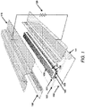
- FIG. 1 illustrates an exemplary configuration of such a conventional DFB ICL.
- a typical DFB ICL in accordance with the prior art includes a laser ridge 101 formed on a chip comprising a GaSb buffer/substrate layer 102 having a bottom cladding layer 103 (typically an InAs/AlSb short-period superlattice) disposed on a top surface thereof.
- a bottom cladding layer 103 typically an InAs/AlSb short-period superlattice
- Laser ridge 101 comprises bottom and top separate confinement layers (SCLs) 104 and 106 (typically lightly n-doped GaSb), with one or more active stages 105 situated between the SCL layers 104/106 and top cladding layer 107 (also typically an InAs/AlSb short-period superlattice) deposited on an upper surface of the top SCL 106.
- SCLs bottom and top separate confinement layers
- active stages 105 situated between the SCL layers 104/106 and top cladding layer 107 (also typically an InAs/AlSb short-period superlattice) deposited on an upper surface of the top SCL 106.
- a grating layer (typically InAs or InAsSb) may be deposited on top of the top SCL to provide a uniform, relatively high-index material into which the grating may be etched. The top portion of this layer is usually n-doped more heavily for electrical contacting.
- a layer of Ge or some other material may alternatively be deposited on top of the structure to receive the grating, in which case the heavily n-doped top InAs or InAsSb contacting layer may be very thin.
- various chirped transition superlattices placed between the various regions that aid the electrical transport from one region to the next.
- An insulating dielectric film 108 (e.g., a thin SiN film) is deposited on the upper surface of the chip including the sidewalls of laser ridge 101 and is removed from the top surface of the ridge, e.g., by lift-off lithography or any other suitable means known to the art.
- a DFB grating 109 is etched into the exposed top grating layer, the thin top cladding layer 107, the other deposited material such as Ge, or some combination of those to produce distributed feedback that is usually sufficient to select lasing in a single spectral mode.
- a metal or combination of metals 110 suitable for contacting n-type InAs or InAsSb (such as Ti/Pt/Au) is then deposited on the entire top surface of the chip to provide contacting for electrical injection, and to provide electrical connection to a metal pad, typically placed to the side of the ridge, large enough for wire bonding.
- the metal 110 lies on top of the deposited dielectric layer 108 to prevent shorting of the top and bottom of the device.
- Power is provided to the laser by means of the top metal contact 110 on top of the ridge 110 and a bottom metal contact layer 111 that is typically deposited on the bottom of the GaSb substrate.
- the top and bottom contacts are connected to opposite terminals of a voltage source 120.
- the upper surface of the ridge 101 into which the DFB grating 109 is patterned is not covered by dielectric film 108, except for a narrow portion near the sidewalls that remains covered by the dielectric 108 to prevent shorting of the sidewalls, electrical contact is made to the entirety of the DFB-patterned laser ridge.
- Some semiconductor laser material systems allow the overgrowth of an electricallyconducting semiconductor with lower refractive index than the modal index to complete the top optical cladding layer and also provide a pathway for injecting electrical current into the semiconductor laser.
- no suitable overgrowth capability is currently available for ICLs grown on GaSb or InAs substrates. Therefore, for ICLs, the top of the grating itself must be metallized to provide the top electrical contact.
- the coupling coefficient decreases exponentially with the top cladding thickness, and so for an ICL emitting at ⁇ ⁇ 3.5 ⁇ m, the top cladding thickness must be reduced to at most ⁇ 500 nm if optical coupling to the grating is to be sufficient to suppress non-resonant longitudinal modes and assure the emission with a narrow linewidth.
- the lasing mode penetrates into the metal contact, introducing additional optical loss that also varies exponentially with the cladding thickness. While the magnitude of the extra loss depends on the contact metallization scheme, as will be discussed further below, a typical value for ICLs with conventional Ti/Pt/Au contacts is 2-3 cm -1 . Since this is comparable to the internal losses originating from all other sources combined, the mode overlap with the lossy metal inevitably degrades the slope and wallplug efficiency. If the top cladding layer is made thinner or the grating is etched deeper to enhance optical coupling to the grating, the loss increases correspondingly.
- the present invention thus provides important improvements to the structure of DFB ICL lasers that will result in reduced internal loss, greater coupling to a DFB grating etched into the top of the waveguide or a deposited material, and lower thermal resistance in ICLs, QCLs, and other classes of semiconductor lasers with substantial current spreading and a given magnitude of internal loss.
- the improved structure provided in accordance with the present invention may also improve the efficiency and maximum output power of either DFB lasers or ridges without gratings that are designed for high power and brightness.
- the present invention provides an approach for reducing the extra loss by reducing the fill factor of the top contact layer, i.e., reducing the percentage of the ridge's top surface in which electrical contact to the metal is made.
- the present invention accomplishes this by providing a plurality of spaced-apart contact openings etched into at least some portion of a dielectric layer situated on top of the laser ridge, which in preferred embodiments is the same dielectric layer that protects the ridge sidewalls and prevents shorting on other portions of the chip.
- the etch into this dielectric layer provide contact between the metal and the exposed grating, InAs or InAsSb top contact layer, or top cladding layer lying below the dielectric, since all other areas of the top surface of the laser ridge are insulated and optically isolated from the metal contact layer by the dielectric.
- a plurality of n contact openings can be formed in the dielectric layer, where the contact openings and spacing between the openings are configured so that a ratio of the total area of the openings to the total area of the laser ridge is less than 100%.
- the structure of an ICL in accordance with the present invention therefore stands in contrast to the structures used in all previous ICLs reported to date, in which all or nearly all of the top of the ridge is exposed to the metal contact layer, i.e., they have top contact layers with fill factors of approximately 100%.
- the contact openings in an ICL in accordance with the present invention can take the form of roughly rectangular "contact stripes" with full coverage perpendicular to the ridge axis and having a predetermined width w and spacing P along the ridge axis, where w and P are configured to provide a predetermined top contact fill factor w / P of less than 100%.
- the openings can have an arbitrary shape.
- the contact openings are regularly spaced and/or symmetrically placed relative to the sides of the ridge, such regular and/or symmetrical placement is not necessary, and in some embodiments, the openings can be placed randomly on the surface of the laser ridge.
- any shape and/or spacing of the contact openings can be used so long as the contact openings are not so far apart that they can't provide uniform current spreading into the laser ridge and so long as the ratio of the total area of the openings to the total area of the laser ridge provides a fill factor of less than 100%.
- the fraction of the internal loss associated with mode overlap with the contact metal is reduced linearly with the reduction in the fill factor of the top contact. For example, if the fill factor is reduced from 100 to 20%, i.e., reduced by a factor of 5, the extra loss is also reduced by about a factor of 5, e.g., to a value ⁇ 1 cm -1 . Such a level of loss may have minimal effect on the device performance because it is smaller than other losses in the laser cavity, whereas a higher value of ⁇ 2-3 cm -1 would usually impose a significant reduction of the device efficiency and maximum output power. Even lower fill factors in the 5-10% range may provide adequate electrical conduction, resulting in further reduction of the additional loss associated with thinning the top cladding layer.
- each contact stripe or other contact opening feature that may be readily patterned with optical lithography with high reliability and high reproducibility is on the order of w ⁇ 10 ⁇ m. Therefore, a typical contact pattern may employ 10 ⁇ m wide stripes on a 50 ⁇ m period, which corresponds to a fill factor of 20%. Narrower stripes and lower fill factors are more easily realized with electron beam lithography, as will be discussed below.
- a further consideration affecting the optimal fill factor is that heat dissipation is generally optimized by maximizing the area over which the semiconductor top surface is in direct physical contact with the top metal layer (that is, high fill factor), without an intervening dielectric layer that imposes additional thermal resistance. Therefore, reducing the fill factor to minimize the optical loss may at some point degrade rather than improve the laser performance because heating of the active stages in the laser core comes to have a greater effect than minimizing the loss. Although this effect has not been investigated systematically to date, the preliminary experimental results discussed below suggest that in some embodiments an intermediate fill factor in the range 14-33% may be optimal.
- the contact openings all have the same width w and same spacing P so that the contact stripes are periodic.
- the placement of the contact openings need not be periodic, so long as none of the gaps between contact openings are larger than the current spreading length and so long as the total spacing between openings provides a low fill factor of less than 100%.
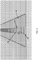
- the contact openings are placed perpendicular to the ridge axis and occupy the center of the ridge, while in other embodiments, the contact openings may be placed near one or both edge of the ridge, parallel to the ridge axis, such that the contact stripes do not occupy the center of the ridge, as shown in FIG. 3 .
- the width w of the contact stripes also can be non-uniform, so long as the average width is configured so that w/P ⁇ 100%.
- each of the n contact stripes with index i formed in the dielectric layer can have a corresponding width w i and be separated from the ( i +1)th neighboring stripe by a corresponding spacing P i such that the ratio of the average of all widths w i to the average of all the distances P i is less than 100%, i.e., w 1 / P l ⁇ 100%.
- the duty cycle of an ICL's top contact layer is directly related to its fill factor if the contact pattern is periodic, i.e., an ICL laser ridge having a periodic top contact pattern with a duty cycle of 20% will also have a fill factor of 20%.
- the terms "low duty cycle contact pattern,” “low duty cycle top contact,” and “low fill factor” contact pattern can be used somewhat interchangeably to describe a contact pattern comprising a series of periodic openings.
- the contact stripes are periodic, their width w and period P can be tuned to produce an ICL having a predetermined duty cycle that optimizes the laser performance at a specified wavelength and temperature range.
- a relatively-large period of P ⁇ 10 ⁇ m is preferable (or the spacing between the contact openings should be at least that large if the pattern is not periodic).
- ICLs are especially advantageous in this regard, since the injected currents are known to spread over large distances on the order of 100 ⁇ m. See, e.g., Forouhar, supra. This is because the top cladding and active regions are both comprised of short-period superlattices that have far lower electrical resistance in the plane than along the growth direction. With such a large distance for current spreading, contact pattern periods of up to 50-200 ⁇ m may be practical, whereas impractically small periods would be needed for most non-cascade semiconductor lasers with very limited current spreading.
- FIGS. 2-4 illustrate aspects of various exemplary embodiments of an ICL having a low-fill factor top contact in accordance with the present invention. It will be noted here that in FIGS. 2-4 and in the description below, where a structural element appears in more than one FIGURE (and appearing in FIG. 1 described above), those elements are denoted by the same reference numeral, with only the first digit being changed to reflect the FIGURE in which they are shown.
- laser ridge 101 shown in FIG. 1 described above corresponds to laser ridge 201 shown in FIG. 2
- laser ridge 301 shown in FIG. 3 and laser ridge 401 shown in FIG. 4 .
- FIG. 2 aspects of a first exemplary embodiment of an interband cascade laser (ICL) having a low-fill-factor top contact in accordance with the present invention is illustrated in the schematic shown in FIG. 2 .
- ICL interband cascade laser
- an exemplary ICL having a low-fill-factor top contact in accordance with the present invention includes a laser ridge 201 formed with the same layers that were discussed above in connection with the conventional DFB ICL structure of FIG 1 . These include a GaSb substrate and buffer layer 202, an InAs/AlSb superlattice bottom cladding layer 203, a bottom GaSb SCL 204, one or more active stages 205, a top GaSb SCL 206, and an InAs/AlSb superlattice top cladding layer 207.
- the DFB ICL in accordance with the embodiment shown in FIG.
- grating layer 209 that extends along some fraction of the length of laser ridge 201, where the grating layer may be a heavily n-doped InAs or InAsSb etching layer, a top cladding layer (e.g., an InAs/AlSb superlattice top cladding layer), or some other suitable material layer such as a Ge layer.
- the top and bottom metal contact layers 210 and 211 provide current flow from voltage source 220 to the laser.
- the top metal contact covers the entire top surface of the laser ridge (apart from narrow stripes adjacent to each sidewall to prevent metal from reaching the sidewalls to create a shorting path) and therefore has a top contact fill factor of about 100%
- the insulating dielectric film 208 such as SiN covers at least some of the top of laser ridge 201 as well as the sidewalls and flat areas adjacent to the laser ridge 201, extending laterally to cover bottom cladding layer 203.
- a plurality of spaced-apart contact openings or "contact stripes” 212 are etched into the dielectric film 208 at the top of the laser ridge to expose the DFB grating layer 209 in the etched areas.
- the contact openings have a predetermined width w and a predetermined periodic spacing P, where P is measured as the distance between corresponding edges of the openings, for example, the distance between the right-hand edges of the openings as shown in FIG. 2 , wherein w and P are configured to provide a predetermined top contact fill factor w/P of less than 100%.
- electrical contact between the metal top contact layer 210 and the laser ridge 201 is only made in the areas patterned for the contact openings, since all other areas of the top surface of the laser ridge are insulated from the metal contact layer by the dielectric 208.
- the spacing P of the contact stripes can be configured to be much larger than the grating period so as to prevent resonant effects due to modulation of the loss and refractive index in the top contact which produce an unintended wavelength selectivity.
- the distribution of the contact stripes may be randomized rather than employing a fixed period P in order to avoid any unintended resonances, although this is not expected to be an issue in most circumstances.
- the structure may optionally be electro-plated with a thick gold layer to improve the heat dissipation and then can be mounted either epitaxial-side-up or epitaxial-side down on a heat sink.
- the contact stripes are formed so that they do not cover the center of the ridge as they do in the embodiment shown in FIG. 2 , but are placed near one or both sides of the ridge and run parallel to the axis of the laser ridge.
- a laser ridge 301 comprising the same layers described above with respect to the conventional configuration of FIG. 1 and the exemplary embodiment of the invention in FIG. 2 can be formed on a substrate and covered with a thin dielectric film 308 as described above with respect to FIG. 2 .
- a series of narrow contact stripes 312 can be formed in the dielectric film 308 to provide a low-fill-factor top contact between the DFB grating layer 309 and the top metal contact.
- the contact stripes 312 occupy regions near one or both sides of the ridge, running parallel to the edges of the ridge along the ridge axis.
- Using e-beam lithography to pattern the stripes in the dielectric should reliably provide contacts as narrow as ⁇ 1-2 ⁇ m, residing ⁇ 1 ⁇ m from each edge of the ridge. See Kim 2007, supra.
- contact stripes 312 form two parallel rows, each line close to the edge of the ridge, while in other embodiments, the contact stripes may occupy only one side of the ridge. In embodiments having two parallel rows of contact stripes, the stripes may be directly opposite one from another so as to be in phase, while in other embodiments, such as that shown in FIG. 3 , the stripes may be out of phase with one another, which has the advantage of minimizing the current spreading distance required for a pattern with a given fill factor.
- the low-duty-cycle contact stripes 312 may also be positioned at random rather than periodic intervals in order to further minimize the potential for distributed feedback at an undesired wavelength.
- the contact stripes impose more loss at the edges of the ridge than in the center, and as a result suppress higher-order lateral modes in a manner similar to the effect of corrugated sidewalls.
- a laser having a low-fill-factor top contact in accordance with the present invention may employ a "pole" deposited in the center of the ridge on top of the grating, where the pole is formed with width roughly half that of the ridge, from Si or another suitable material having a relatively high refractive index.
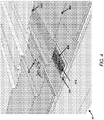
- FIG. 4 illustrates aspects of an exemplary configuration of this embodiment of the present invention.
- a laser ridge 401 is formed on a substrate.
- the layer structure of laser ridge 401 is the same as that described above with respect to FIGS. 1 and 2 and therefore will not be described in detail here.
- the laser structure also includes DFB grating layer 409 on top of the laser ridge 401, where the DFB grating layer may be an n-doped InAs or InAsSb etching layer, an InAs/AlSb superlattice top cladding layer, or some other suitable material layer such as a Ge layer.
- the contact openings 412 are periodic, with the stripes having a width w and a spacing P configured to provide a low-fill-factor top contact layer in the manner described above with respect to FIG. 2 .
- a thin pole layer 413 of Si or some other material having a high refractive index relative to the contact metal or the dielectric is deposited in the middle portion of the ridge on top of DFB grating layer 409 before the dielectric layer 408 is deposited.
- Depositing this additional material with high refractive index near the center of the ridge effectively raises the refractive index in the central portion of the ridge and enhances selection of the desired fundamental lateral mode which has its highest intensity at the center of the ridge.
- NNL Naval Research Laboratory
- the presence of this Si pole layer 413 in the ICL structure in this embodiment further lowers the loss by providing additional separation between the lasing mode and the top metal contact, since in the center of the ridge the metal now resides on top of both the insulating layer 408 and the Si pole layer 413 as well as the etching layer or other deposited material such as Ge.
- the contact stripes are placed near the edges of the ridge, parallel to the ridge axis, and do not cover the central portion of the ridge, as shown in FIG. 3 . In other embodiments, the contact stripes can be placed perpendicular to the ridge axis to provide full coverage of the central portion of the ridge, as shown in FIG. 2 .
- the contact stripes 412 shown in FIG. 4 are uniform, periodic, and parallel to the axis of the laser ridge, one skilled in the art will recognize that the other configurations of the contact stripes described herein are also possible within the scope of this embodiment, i.e., the stripes can be non-uniform, nonperiodic, and/or perpendicular to the axis of the laser ridge, so long as the contact openings are not so far apart that they can't provide uniform current spreading into the laser ridge and so long as the ratio of the total area of the openings to the total area of the laser ridge provides a fill factor of less than 100%.
- a SiN dielectric insulating layer was deposited on the top and sides of the ridge before metallization, after which optical lithography was used to pattern contact stripes in the insulating film with a periodic low-duty-cycle pattern as illustrated in FIG 2 .
- the results were compared to those for ridges having the conventional design in which the metal contact covered the entire top surface of the ridge (as in FIG 1 , only without the DFB grating), which corresponds to a contact duty cycle of 100%.
- the plots in FIG. 5 show the resulting cw light-current characteristics measured for the structures having the 10%, 20%, 50%, and 100% duty cycles. As can be seen from the plots in FIG. 5 , the slope efficiency for the device with 20% duty cycle is improved by >70% relative to the unpatterned control sample having a 100% duty cycle, while the threshold current is reduced by nearly a factor of 2.
- FIGS. 6A and 6B plot analogous pulsed results for the dependences of threshold current density J th and slope efficiency on periodic contact duty cycle for two thin-top-cladding ICL devices with each duty cycle, where FIG. 6A shows the pulsed threshold current density at room temperature vs. contact duty cycle for thin-top-cladding ICLs (19- ⁇ m-wide, 2-mm-long ridges) and FIG. 6B shows the pulsed slope efficiency at room temperature vs. contact duty cycle.
- the lasing threshold current density J th decreases and the laser efficiency ( FIG. 6B ) increases as the duty cycle is reduced.
- the lasing threshold continues to decrease and the efficiency continues to increase down to the lowest duty cycle of 10%.
- the low-fill-factor top contact structure of the present invention was applied to DFB ICLs operating at a wavelength around 3.3 ⁇ m.
- the ICL structure was grown on a GaSb substrate with a layering design similar to that for the wafer employed in the first reduction to practice discussed above, except that the top InAs layer was 250 nm thick to provide a grating layer into which the DFB grating could be etched. Only the top 20 nm of this structure was heavily doped (to 5 ⁇ 10 18 cm -3 ), whereas in a more preferred embodiment of the invention, the entire grating layer would have been heavily doped.
- the InAs was not lattice-matched to the GaSb substrate, that layer relaxed and exhibited a cross-hatched morphology. Nevertheless, most of the DFBs with grating pitches in the range 558-568 nm lased in a single spectral mode for at least some ranges of temperatures and currents.
- This lot of devices did not employ the low-loss Ag or Ti-Ag contacts of some embodiments of the invention, but instead used conventional Ti/Pt/Au layers for the top contact metal.
- FIG. 7 shows the cw light-current characteristics measured for one series of DFB ICL ridges having varying contact duty cycles (14-100%), where the ridges were about 4.5 ⁇ m wide and 2 mm long and were mounted epitaxial-side-up with uncoated facets and gold electroplating for heat dissipation.
- These devices all lased in a single spectral mode at some range of temperatures and currents, although some only at temperatures above 25 °C. Note from the figure that the observed slopes are highest for the devices with 20% and 33% duty cycles, and that both the threshold current and the slope efficiency are much worse for the device with 100% duty cycle.
- the tendency to lase in a single spectral mode did not show any apparent dependence on contact duty cycle.
- the highest cw power emitted in a single spectral mode was 6.8 mW for the DFB with 33% duty cycle.
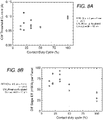
- FIGS. 8A and 8B plot the corresponding threshold currents and differential slope efficiencies vs. duty cycle for all of the DFB ICLs that were tested, where FIG. 8A shows the threshold current for continuous-wave lasing at room temperature vs. contact duty cycle for DFB ICLs (at least two DFB devices with each duty cycle being measured), and FIG. 8B shows the cw differential slope efficiency at room temperature vs. contact duty cycle for the same DFB ICLs as in FIG. 8A .
- a primary advantage of the low-duty-cycle top contact of the invention is that semiconductor lasers constructed from materials subject to substantial current spreading may use a thin top cladding layer and yet maintain low internal loss induced by overlap of the optical mode with the contact metallization.
- the invention will be especially advantageous when applied to high-power interband cascade lasers, and to single-mode DFB ICLs emitting high powers with high efficiency.
- the combination of a heavily-doped InAs 0.91 Sb 0.09 top grating/capping layer with the low-duty-cycle top contact metallization will maximize the maximum output power and efficiency of DFB ICLs while maintaining high processing yield with a fully strain balanced structure.
- the present invention encompasses several variations on the preferred embodiments presented above. Although the details may vary somewhat, the invention's advantages apply equally to any ICL core design, emission wavelength, type-II or type-I active quantum wells, etc.
- the invention may also be advantageous when applied to quantum cascade lasers (QCLs), since those devices can also exhibit substantial current spreading. See A. Lyakh, P. Zory, D. Wasserman, G. Shu, C. Gmachl, M. D'Souza, D. Botez, and D. Bour, “Narrow Stripe-Width, Low-Ridge High Power Quantum Cascade Lasers," Appl. Phys. Lett. 90, 141107 (2007 ).
- QCLs grown on InP or GaAs substrates may employ a regrowth step following the grating etch to provide low-loss DFB devices, that additional step adds to the production expense and can negatively influence the processing yield.
- diode laser types or specific device geometries may exist that also exhibit sufficient current spreading (more than about 20 ⁇ m) for the invention to be effective, in most cases the invention will not be applicable to conventional diode lasers because in such devices the current spreading is insufficient to maintain uniform current injection if a reasonable patterning period is employed.
- one type of device for which the invention can be used advantageously to reduce the threshold current and increase the output efficiency is a single-mode ICL with a DFB grating on top of the ridge, since a thin top cladding layer is mandatory in such a structure to assure adequate coupling of the optical mode to the grating.
- This approach may employ either Ti/Pt/Au contacts or (Ti)/Ag contacts for lower loss, although the limitations discussed above concerning relaxation of the grating layer when non-lattice-matched InAs is employed, or the diffusion of Ag into the epi-layer during the bottom contact anneal when lattice-matched InAsSb is employed, also apply to this embodiment. With very low fill factors being possible, however, the optical loss associated with employing Ti/Pt/Au contacts may be relatively insignificant.
- the final layer of the epitaxial growth by molecular beam epitaxy is an n + -InAs capping layer that provides low electrical resistance after the Ti/Pt/Au or Ag contact is deposited.
- MBE molecular beam epitaxy
- InAs is not lattice-matched to GaSb, unlike the rest of the epitaxial structure, the defects associated with strain relaxation are usually not severe because the typical thickness of the InAs capping layer is only about 20 nm.
- the capping layer Two possibilities for the capping layer are the InAs 0.91 Sb 0.09 alloy, which has properties similar to InAs (with slightly smaller bandgap) but is lattice-matched to GaSb, or the same short-period InAs/AlSb superlattice that is employed for the optical cladding layers (combined with a thin, more heavily-doped superlattice or InAs capping layer).
- the InAsSb option is preferable from the contacting standpoint, although NRL experiments indicate that a superlattice contact may also be acceptable.
- a second significant limitation of using moderately-doped ( ⁇ 10 17 cm -3 ) InAs as the relatively-thick grating layer material is that interband absorption will degrade the output power and efficiency at any lasing wavelength below about 3.5 ⁇ m, and will most likely preclude lasing at any wavelength shorter than about 3.2 ⁇ m. With its even smaller energy gap, moderately-doped InAs 0.91 Sb 0.09 begins to absorb wavelengths as long as about 4.6 ⁇ m, and will strongly absorb at ⁇ ⁇ 4.1 ⁇ m.
- Undoped InAs and InAsSb absorb quite strongly any wavelength shorter than their energy gaps of 3.5 and 4.6 um, respectively. These wavelength limits become somewhat longer, due to the Burstein-Moss shift of the energy gap imposed by band filling within the conduction band, when the layers are doped to 5 ⁇ 10 17 cm -3 to insure good electrical transport.
- the maximum photon energy for lasing must be 2 k B T (where k B is the Boltzmann constant and T is temperature) smaller than the difference between the electron and hole quasi-Fermi energies (since some fraction of the electron states below the Fermi level remain unoccupied), the minimum photon energies for which lasing may be expected to occur decrease to about 3.2 and 4.1 ⁇ m, respectively.
- a Ti/Pt/Au contact can be employed in conjunction with a lattice-matched InAs 0.91 Sb 0.09 (or InAs/AlSb superlattice) grating layer, while still reducing the internal loss because only a fraction of the mode penetrating to the top of the epitaxial layer actually encounters any metal.
- the InAs 0.91 Sb 0.09 capping layer can be heavily n-doped to ⁇ 2 ⁇ 10 18 cm- 3 , with ⁇ 2.5 ⁇ 10 18 cm -3 being preferred, with the doping being throughout the entire layer rather than just in the top capping layer used to make electrical contact. This will have the effect of inducing a substantial Burstein-Moss shift of the effective bandgap to a much shorter wavelength. With this modification, interband absorption losses will remain negligible in DFB ICLs emitting at wavelengths below 3 ⁇ m.
- the additional free carrier absorption loss associated with the heavy doping will be no greater than about 0.1 cm -1 , which is insignificant compared to other internal losses in the waveguide.
- the entire grating layer is doped to much more than 2.5 ⁇ 10 18 cm -3 , the resulting plasma-driven reduction of the refractive index will reduce the coupling strength of the DFB grating.
- the low-fill-factor top contact layer of the present invention reduces the loss associated with a Ti/Pt/Au contact deposited on top of a DFB grating etched into the grating layer of a conventional ICL structure having a thin top cladding layer, the use of those metals still induces additional loss that lowers the device efficiency and maximum output power. Even using the low-fill-factor contacts of the invention, it is still preferable to employ low-loss Ag or Ti/Ag (with the Ti only ⁇ 10 nm thick) for the top contact.
- Another embodiment of the invention therefore reorders the usual processing steps to form the Cr/Pt/Au bottom contact (to the GaSb or InAs substrate) with its high-temperature anneal before the top contact is formed, and then deposit the top contact at a later stage.
- This has the advantage of eliminating the need for a high-temperature anneal after the top Ag metallization has been deposited, since annealing when the Ag is present causes the unacceptable extensive Ag diffusion into the grating layer that was discussed above.
- a primary disadvantage of this approach is that in order to assure a high facet quality when the die is cleaved into laser cavities, the wafer must first be thinned to ⁇ 200-250 ⁇ m before the bottom contact is deposited. NRL experiments found that handling of the thinner die throughout all the subsequent processing steps substantially increases the occurrence of unintended breakage, thereby reducing the device yield. It may be possible to mitigate this shortcoming by developing revised processing protocols. In another embodiment, the die thinning step may be eliminated to preserve high handling yield, although the cleave quality and yield may then degrade.
- the bottom contact is deposited after the Ag or Ti/Ag top contact as in the conventional processing, but the annealing step is omitted.
- An NRL reduction to practice of this approach found that failure to anneal the Cr/Pt/Au bottom contact introduced at least 1.1 V of additional voltage barrier to the bias required to operate the laser. The additional voltage will increase the device's threshold drive power and decrease the wallplug efficiency.
- the short-period InAs/AlSb superlattice used as the top cladding material in most ICL designs has very low thermal conductivity, it may be advantageous to employ a thinner top cladding than in conventional designs in conjunction with use of the invention to mitigate the additional internal losses that occur when the lasing mode has increased overlap with the top contact metallization. Since the thermal path from the device's active core to the heat sink is shortened, the temperature increase caused by any given injection conditions will be lower.
- the employment of Ti/Pt/Au top contact metal may induce relatively low optical loss because the fill factor is significantly less than 100%.
- (Ti)/Ag top contact metal may be employed to reduce the loss further. Since the Ge top grating obviates any need to etch into the semiconductor, the top of the epitaxial structure may be either n + -InAsSb or a thin, unrelaxed n + -InAs top contact layer without any degradation of the grating quality during the anneal of the bottom contact.
- One potential advantage of using e-beam lithography is that it becomes practical to pattern top contacts with fill factors ⁇ 10%, but which are spaced closely enough that the current spreading provides uniform current injection.
- Narrow ridges with low top contact duty cycle for low internal loss, straight sidewalls for low scattering loss, and relatively short cavities for low active area should be optimal for minimizing the threshold drive power, a critical metric for many chemical sensing systems based on mid-IR laser spectroscopy.
- the reduction of active device area is advantageous only up to a point. NRL experiments found that the minimum optimal ridge width is ultimately limited by excessive sidewall scattering that occurs for ridges narrower than ⁇ 5 ⁇ m, while the minimum cavity length is limited by an increase in the current threshold for cavities shorter than ⁇ 1 mm.
- the primary objective is to maximize the output power attainable in a single spectral mode
- Corrugated sidewalls suppress higher-order lateral lasing modes, since those are selectively scattered due to their higher intensity near the ridge boundaries. See, e.g., C. S. Kim, M. Kim, W. W. Bewley, J. R. Lindle, C. L. Canedy, J. Abell, I. Vurgaftman, and J. R. Meyer, "Corrugated-sidewall interband cascade lasers with single-mode midwave-infrared emission at room temperature," Appl. Phys. Lett. 95, 231103 (2009 ) ("Kim 2009").
- the corrugations also reduce the slope efficiency slightly (typically ⁇ 10%) due to additional scattering of the fundamental mode at the sidewalls, the larger active area of a wider ridge provides a net gain in power.
- ⁇ ⁇ 3.5 ⁇ m a single lateral mode can be maintained to widths on the order of 10-12 ⁇ m when the sidewalls are corrugated, but only 5-7 ⁇ m when the sidewalls are straight.
- NRL has studied corrugation periods from 2-16 ⁇ m, and corrugation amplitudes from 2-3.5 ⁇ m.
- a larger corrugation period is found to provide better beam quality with slightly higher lasing threshold and slightly lower slope efficiency. Since a larger period has the further advantage of being much less difficult to process reliably and reproducibly, ridges with sidewalls having a corrugation period of ⁇ 10 ⁇ m and an amplitude of ⁇ 2 ⁇ m are preferred in some embodiments.
Landscapes
- Physics & Mathematics (AREA)
- Condensed Matter Physics & Semiconductors (AREA)
- General Physics & Mathematics (AREA)
- Electromagnetism (AREA)
- Optics & Photonics (AREA)
- Acoustics & Sound (AREA)
- Semiconductor Lasers (AREA)
- Geometry (AREA)
Claims (15)
- Laser à cascade interbande, ICL, à rétroaction répartie, DFB, ou laser à cascade quantique, QCL, comportant un contact de sommet à faible facteur de remplissage, comprenant :une nervure de laser (201) qui est formée sur un substrat, la nervure de laser comprenant :une couche de gainage de fond en super-réseau (203) ;une région de gain active (205) qui est disposée au-dessus de la couche de gainage de fond (203) ;une couche de réseau DFB (209) qui comporte un réseau DFB qui est formé dans une couche semiconductrice qui est disposée au-dessus de la région de gain active (205) ;une couche de gainage de sommet en super-réseau (207) qui présente une épaisseur prédéterminée et qui est disposée entre la couche de réseau DFB (209) et la région de gain active (205) ; etun film isolant diélectrique (208) qui est disposé sur une surface supérieure de la couche de réseau DFB (209) et qui recouvre la surface supérieure de la nervure de laser (201) ;dans lequel le film isolant diélectrique (208) comporte une pluralité prédéterminée d'ouvertures de contact répétées et espacées les unes des autres (212) qui sont formées en son sein et qui courent suivant une longueur longitudinale de la nervure de laser (201), chacune des ouvertures de contact étant étendue latéralement au travers de la surface supérieure de la nervure de laser perpendiculairement à un axe longitudinal de la nervure de laser (201) et étant séparée d'une ouverture de contact voisine (212) par un espacement qui présente une largeur d'au moins 10 µm ;la nervure de laser (201) incluant en outre un contact en métal de sommet (210) qui est disposé sur une surface supérieure du film isolant diélectrique (208), le contact en métal de sommet étant connecté à une source de tension (220) pour assurer un contact électrique par rapport à la nervure de laser seulement dans les zones qui sont exposées par les ouvertures de contact (212) ; dans lequel des zones du sommet de la nervure de laser (201) à l'exception des ouvertures de contact (212) sont séparées de la couche de contact en métal (210) par le film isolant diélectrique (208) ; etdans lequel une dimension et un espacement des ouvertures de contact (212) sont configurés pour assurer un facteur de remplissage prédéterminé inférieur à 100 % dans le contact en métal de sommet (210) qui assure une perte interne prédéterminée associée à un chevauchement entre le mode d'émission laser et le contact en métal de sommet.
- Laser DFB comportant un contact de sommet à faible facteur de remplissage selon la revendication 1, dans lequel au moins une caractéristique parmi une dimension et une forme des ouvertures de contact (212) est aléatoire.
- Laser DFB comportant un contact de sommet à faible facteur de remplissage selon la revendication 1, dans lequel chacune des ouvertures de contact (212) présente une largeur correspondante wi et est séparée d'une (i + 1)-ième ouverture de contact voisine (212) par un espacement correspondant Pi, dans lequel toutes les largeurs wi et tous les espacements Pi sont configurés de telle sorte que le rapport de la moyenne de toutes les largeurs wi sur la moyenne de toutes les distances/tous les espacements Pi soit inférieur à 100 %.
- Laser DFB comportant un contact de sommet à faible facteur de remplissage selon la revendication 1, dans lequel les ouvertures de contact (212) sont situées de telle sorte que les ouvertures de contact soient étendues au travers d'un axe qui court longitudinalement au travers d'un centre de la nervure de laser (201).
- Laser en cascade interbande DFB comportant un contact de sommet à faible facteur de remplissage selon la revendication 1, dans lequel la couche de réseau DFB (209) est une couche en Ge, en InAs ou en InAsSb ou une couche de super-réseau en InAs/AISb.
- Laser DFB comportant un contact de sommet à faible facteur de remplissage selon la revendication 1, comprenant en outre une couche de pôle (413) qui présente un indice de réfraction élevé par rapport au film isolant diélectrique (408) et qui est située à proximité du centre de la nervure de laser (401) entre la couche de réseau DFB (409) et le film isolant diélectrique (408).
- Laser à cascade interbande, ICL, à rétroaction répartie, DFB, ou laser à cascade quantique, QCL, comportant un contact de sommet à faible facteur de remplissage, comprenant :une nervure de laser (301) qui est formée sur un substrat, la nervure de laser comprenant :une couche de gainage de fond en super-réseau ;une région de gain active qui est disposée au-dessus de la couche de gainage de fond ;une couche de réseau DFB (309) qui comporte un réseau DFB qui est formé dans une couche semiconductrice qui est disposée au-dessus de la région de gain active ;une couche de gainage de sommet en super-réseau qui est disposée entre la couche de réseau DFB (309) et la région de gain active ; etun film isolant diélectrique (308) qui est disposé sur une surface supérieure de la couche de réseau DFB (309) et qui recouvre la surface supérieure de la nervure de laser (301) ;dans lequel le film isolant diélectrique (308) comporte une pluralité prédéterminée d'ouvertures de contact répétées et espacées les unes des autres (312) qui sont formées en son sein et qui courent suivant une longueur longitudinale de la nervure de laser (301), les ouvertures de contact étant agencées dans deux rangées parallèles qui ne recouvrent pas le centre de la nervure de laser, chaque rangée étant située à proximité d'un bord externe de la nervure de laser, parallèlement à un axe longitudinal de la nervure de laser (301), chacune des ouvertures de contact (312) étant séparée d'une ouverture de contact voisine par un espacement qui présente une largeur d'au moins 10 µm suivant l'axe longitudinal ;la nervure de laser (301) incluant en outre un contact en métal de sommet qui est disposé sur une surface supérieure du film isolant diélectrique (308), le contact en métal de sommet étant connecté à une source de tension pour assurer un contact électrique par rapport à la nervure de laser seulement dans les zones qui sont exposées par les ouvertures de contact (312) ; dans lequel des zones du sommet de la nervure de laser (301) à l'exception des ouvertures de contact (312) sont séparées de la couche de contact en métal par le film isolant diélectrique (308) ; etdans lequel une dimension et un espacement des ouvertures de contact (312) sont configurés pour assurer un facteur de remplissage prédéterminé inférieur à 100 % dans le contact en métal de sommet suivant un axe de la nervure de laser (301) qui assure une perte interne prédéterminée associée à un chevauchement entre le mode d'émission laser et le contact en métal de sommet.
- Laser DFB comportant un contact de sommet à faible facteur de remplissage selon la revendication 7, dans lequel au moins une caractéristique parmi une dimension et une forme des ouvertures de contact (312) dans l'une des rangées d'ouvertures de contact ou dans les deux rangées d'ouvertures de contact est aléatoire.
- Laser DFB comportant un contact de sommet à faible facteur de remplissage selon la revendication 7, dans lequel chacune des ouvertures de contact (312) présente une largeur correspondante wi et est séparée d'une (i + 1)-ième ouverture de contact voisine par un espacement correspondant Pi, dans lequel toutes les largeurs wi et tous les espacements Pi sont configurés de telle sorte que le rapport de la moyenne de toutes les largeurs wi sur la moyenne de toutes les distances/tous les espacements Pi soit inférieur à 100 %.
- Laser DFB comportant un contact de sommet à faible facteur de remplissage selon la revendication 7, dans lequel les ouvertures de contact comprennent deux rangées parallèles dont chacune est située à proximité d'un bord externe de la nervure de laser (301) de telle sorte que les ouvertures de contact ne recouvrent pas le centre de la nervure de laser, et dans lequel les ouvertures de contact dans les deux rangées parallèles sont configurées de manière à ce qu'elles soient alignées mutuellement en phase.
- Laser DFB comportant un contact de sommet à faible facteur de remplissage selon la revendication 7, dans lequel les ouvertures de contact comprennent deux rangées parallèles dont chacune est située à proximité d'un bord externe de la nervure de laser (301) de telle sorte que les ouvertures de contact ne recouvrent pas le centre de la nervure de laser, et dans lequel les ouvertures de contact (312) dans les deux rangées parallèles sont configurées de manière à ce qu'elles soient alignées mutuellement en déphasage.
- Laser en cascade interbande DFB comportant un contact de sommet à faible facteur de remplissage selon la revendication 7, dans lequel la couche de réseau DFB (309) est une couche en Ge, en InAs ou en InAsSb ou une couche de super-réseau en InAs/AISb.
- Laser DFB comportant un contact de sommet à faible facteur de remplissage selon la revendication 7, comprenant en outre une couche de pôle (413) qui présente un indice de réfraction élevé par rapport au film isolant diélectrique (408) et qui est située à proximité du centre de la nervure de laser (401) entre la couche de réseau DFB (409) et le film isolant diélectrique (408).
- Laser DFB comportant un contact de sommet à faible facteur de remplissage selon la revendication 1, dans lequel une distribution des ouvertures de contact (212) est aléatoire.
- Laser DFB comportant un contact de sommet à faible facteur de remplissage selon la revendication 7, dans lequel une distribution des ouvertures de contact (312) dans l'une des rangées d'ouvertures de contact ou dans les deux rangées d'ouvertures de contact est aléatoire.
Applications Claiming Priority (4)
| Application Number | Priority Date | Filing Date | Title |
|---|---|---|---|
| US201562171269P | 2015-06-05 | 2015-06-05 | |
| US201562209554P | 2015-08-25 | 2015-08-25 | |
| US201562251154P | 2015-11-05 | 2015-11-05 | |
| PCT/US2016/035652 WO2017039767A1 (fr) | 2015-06-05 | 2016-06-03 | Lasers à cascade interbandes avec contact supérieur à faible facteur de remplissage pour réduction de perte |
Publications (3)
| Publication Number | Publication Date |
|---|---|
| EP3304660A1 EP3304660A1 (fr) | 2018-04-11 |
| EP3304660A4 EP3304660A4 (fr) | 2019-02-13 |
| EP3304660B1 true EP3304660B1 (fr) | 2022-10-26 |
Family
ID=57452374
Family Applications (1)
| Application Number | Title | Priority Date | Filing Date |
|---|---|---|---|
| EP16842456.2A Active EP3304660B1 (fr) | 2015-06-05 | 2016-06-03 | Lasers à cascade interbandes avec contact supérieur à faible facteur de remplissage pour réduction de perte |
Country Status (4)
| Country | Link |
|---|---|
| US (1) | US9923338B2 (fr) |
| EP (1) | EP3304660B1 (fr) |
| JP (1) | JP2018518053A (fr) |
| WO (1) | WO2017039767A1 (fr) |
Families Citing this family (10)
| Publication number | Priority date | Publication date | Assignee | Title |
|---|---|---|---|---|
| US10297699B2 (en) | 2016-05-27 | 2019-05-21 | The United States Of America, As Represented By The Secretary Of The Navy | In-plane resonant-cavity infrared photodetectors with fully-depleted absorbers |
| JP2019519120A (ja) | 2016-06-24 | 2019-07-04 | ザ ガバメント オブ ザ ユナイテッド ステイツ オブ アメリカ,アズ リプレゼンテッド バイ ザ セクレタリー オブ ザ ネイビー | 成長したトップクラッド層を全く有しないか、又は薄いトップクラッド層を有する弱屈折率導波型インターバンドカスケードレーザ |
| US20180323580A1 (en) * | 2017-05-08 | 2018-11-08 | Thorlabs Quantum Electronics, Inc. | Distributed feedback interband cascade lasers with corrugated sidewall |
| CN107611776B (zh) * | 2017-10-13 | 2020-06-09 | 中国科学院长春光学精密机械与物理研究所 | 一种增益耦合分布反馈半导体激光器及其制作方法 |
| US10340661B2 (en) | 2017-11-01 | 2019-07-02 | International Business Machines Corporation | Electro-optical device with lateral current injection regions |
| EP3821505A4 (fr) | 2018-07-13 | 2022-07-06 | The Government of the United States of America as represented by the Secretary of the Navy | Capteurs et lasers semi-conducteurs très stables pour des circuits intégrés photoniques sur iii-v et sur silicium |
| CN111641103B (zh) * | 2020-06-09 | 2022-07-01 | 厦门市三安光电科技有限公司 | 一种激光二极管及其制造方法 |
| US12586987B2 (en) | 2022-01-04 | 2026-03-24 | The Government Of The United States Of America, As Represented By The Secretary Of The Navy | Weak index guiding of interband cascade lasers |
| CN118137294B (zh) * | 2024-05-07 | 2024-07-19 | 中国科学院半导体研究所 | 带间级联激光器阵列芯片及其制备方法 |
| WO2026008234A1 (fr) | 2024-07-02 | 2026-01-08 | Alpes Lasers S.A. | Laser à cascade interbande à rétroaction distribuée |
Family Cites Families (24)
| Publication number | Priority date | Publication date | Assignee | Title |
|---|---|---|---|---|
| US4400813A (en) * | 1981-07-20 | 1983-08-23 | Bell Telephone Laboratories, Incorporated | Crenelated-ridge waveguide laser |
| JPS62295480A (ja) * | 1986-06-16 | 1987-12-22 | Mitsubishi Electric Corp | 半導体レ−ザ装置 |
| TW289175B (fr) * | 1995-04-07 | 1996-10-21 | Mitsubishi Electric Corp | |
| US5588015A (en) | 1995-08-22 | 1996-12-24 | University Of Houston | Light emitting devices based on interband transitions in type-II quantum well heterostructures |
| US5799026A (en) | 1996-11-01 | 1998-08-25 | The United States Of America As Represented By The Secretary Of The Navy | Interband quantum well cascade laser, with a blocking quantum well for improved quantum efficiency |
| JP2000012963A (ja) | 1998-06-23 | 2000-01-14 | Nec Corp | 光半導体装置の製造方法 |
| US6324199B1 (en) * | 1998-11-18 | 2001-11-27 | Lucent Technologies Inc. | Intersubband light source with separate electron injector and reflector/extractor |
| JP3739071B2 (ja) * | 1999-01-25 | 2006-01-25 | パイオニア株式会社 | 分布帰還リッジ型半導体レーザ及びその製造方法 |
| US6501783B1 (en) * | 2000-02-24 | 2002-12-31 | Lucent Technologies Inc. | Distributed feedback surface plasmon laser |
| US6463088B1 (en) * | 2000-07-07 | 2002-10-08 | Lucent Technologies Inc. | Mesa geometry semiconductor light emitter having chalcogenide dielectric coating |
| US7269195B2 (en) * | 2002-03-04 | 2007-09-11 | Quintessence Photonics Corporation | Laser diode with an amplification section that has a varying index of refraction |
| JP2005166998A (ja) | 2003-12-03 | 2005-06-23 | Mitsubishi Electric Corp | リッジ型分布帰還半導体レーザ |
| DE602004024451D1 (de) * | 2003-12-22 | 2010-01-14 | Panasonic Corp | Halbleiterlaser-bauelement und laserprojektor |
| GB2427752A (en) * | 2005-06-28 | 2007-01-03 | Bookham Technology Plc | High power semiconductor laser diode |
| JP4928988B2 (ja) * | 2007-03-07 | 2012-05-09 | 日本オプネクスト株式会社 | 半導体光装置およびその製造方法 |
| US8387378B2 (en) | 2008-07-29 | 2013-03-05 | Caterpillar Inc. | Hydraulic system having automated ride control activation |
| US8125706B2 (en) | 2008-10-20 | 2012-02-28 | The United States Of America As Represented By The Secretary Of The Navy | High-temperature interband cascade lasers |
| US20120106583A1 (en) * | 2010-11-02 | 2012-05-03 | Onechip Photonics Inc. | Vertically-coupled surface-etched grating dfb laser |
| US8290011B2 (en) | 2010-11-22 | 2012-10-16 | The United States Of America, As Represented By The Secretary Of The Navy | Interband cascade lasers |
| EP2702648B1 (fr) | 2011-04-20 | 2018-05-09 | The Government of the United States of America as represented by the Secretary of the Navy | Lasers à cascade interbandes à densités de porteurs calculées |
| DE102011103952B4 (de) * | 2011-06-10 | 2022-05-05 | OSRAM Opto Semiconductors Gesellschaft mit beschränkter Haftung | Kantenemittierender Halbleiterlaser |
| DE102012111512B4 (de) * | 2012-11-28 | 2021-11-04 | OSRAM Opto Semiconductors Gesellschaft mit beschränkter Haftung | Halbleiterstreifenlaser |
| US10371898B2 (en) * | 2013-09-05 | 2019-08-06 | Southern Methodist University | Enhanced coupling strength grating having a cover layer |
| US9590389B2 (en) * | 2014-10-31 | 2017-03-07 | Nichia Corporation | Semiconductor laser element |
-
2016
- 2016-06-03 JP JP2017561418A patent/JP2018518053A/ja active Pending
- 2016-06-03 WO PCT/US2016/035652 patent/WO2017039767A1/fr not_active Ceased
- 2016-06-03 US US15/172,338 patent/US9923338B2/en active Active
- 2016-06-03 EP EP16842456.2A patent/EP3304660B1/fr active Active
Also Published As
| Publication number | Publication date |
|---|---|
| JP2018518053A (ja) | 2018-07-05 |
| WO2017039767A1 (fr) | 2017-03-09 |
| US20160359298A1 (en) | 2016-12-08 |
| EP3304660A4 (fr) | 2019-02-13 |
| US9923338B2 (en) | 2018-03-20 |
| EP3304660A1 (fr) | 2018-04-11 |
Similar Documents
| Publication | Publication Date | Title |
|---|---|---|
| EP3304660B1 (fr) | Lasers à cascade interbandes avec contact supérieur à faible facteur de remplissage pour réduction de perte | |
| JP5717726B2 (ja) | 大出力パワー用の横結合を持つdfbレーザダイオード | |
| US6326646B1 (en) | Mounting technology for intersubband light emitters | |
| EP2957004B1 (fr) | Laser à rétroaction distribuée couplé transversalement à croissance en une seule étape | |
| US9960571B2 (en) | Weakly index-guided interband cascade lasers with no grown top cladding layer or a thin top cladding layer | |
| US20050063440A1 (en) | Epitaxial mode-confined vertical cavity surface emitting laser (VCSEL) and method of manufacturing same | |
| US11757251B2 (en) | Quantum cascade laser system with angled active region | |
| US20070223549A1 (en) | High-Power Optoelectronic Device with Improved Beam Quality Incorporating A Lateral Mode Filtering Section | |
| US6907056B2 (en) | Semiconductor light sources with doping gradients in optical confinement layers for improved device efficiency | |
| US7031365B2 (en) | Locally-outcoupled cavity resonator having unidirectional emission | |
| WO2003081736A1 (fr) | Laser a semi-conducteur thz comprenant un guide d'onde de confinement a modes plasmoniques regules | |
| US20050201437A1 (en) | Semiconductor laser | |
| Lauer et al. | InP‐based long‐wavelength vertical‐cavity surface‐emitting lasers with buried tunnel junction | |
| US8428093B2 (en) | High-power quantum cascade lasers with active-photonic-crystal structure for single, in-phase mode operation | |
| Deubert et al. | High-power quantum dot lasers with improved temperature stability of emission wavelength for uncooled pump sources | |
| US8416824B2 (en) | Surface emitting laser with current constriction layer and multiple active regions | |
| US7561607B2 (en) | Laser source with broadband spectrum emission | |
| Tredicucci et al. | Advances in THz quantum cascade lasers: fulfilling the application potential | |
| Lee et al. | Asymmetric broad waveguide diode lasers (/spl lambda/= 980 nm) of large equivalent transverse spot size and low temperature sensitivity | |
| Swint et al. | Curved waveguides for spatial mode filters in semiconductor lasers | |
| US12431688B1 (en) | Distributed Bragg reflector quantum cascade lasers | |
| WO2024105723A1 (fr) | Structure à puits quantiques multiples, laser à semi-conducteur et procédé de fabrication d'une structure à puits quantiques multiples | |
| Pospiech et al. | Laser diodes | |
| US20160164249A1 (en) | Semiconductor laser diode and laser array implementing the same | |
| Liu et al. | Introduction of High Power Semiconductor Lasers |
Legal Events
| Date | Code | Title | Description |
|---|---|---|---|
| STAA | Information on the status of an ep patent application or granted ep patent |
Free format text: STATUS: THE INTERNATIONAL PUBLICATION HAS BEEN MADE |
|
| PUAI | Public reference made under article 153(3) epc to a published international application that has entered the european phase |
Free format text: ORIGINAL CODE: 0009012 |
|
| STAA | Information on the status of an ep patent application or granted ep patent |
Free format text: STATUS: REQUEST FOR EXAMINATION WAS MADE |
|
| 17P | Request for examination filed |
Effective date: 20171117 |
|
| AK | Designated contracting states |
Kind code of ref document: A1 Designated state(s): AL AT BE BG CH CY CZ DE DK EE ES FI FR GB GR HR HU IE IS IT LI LT LU LV MC MK MT NL NO PL PT RO RS SE SI SK SM TR |
|
| AX | Request for extension of the european patent |
Extension state: BA ME |
|
| DAV | Request for validation of the european patent (deleted) | ||
| DAX | Request for extension of the european patent (deleted) | ||
| A4 | Supplementary search report drawn up and despatched |
Effective date: 20190116 |
|
| RIC1 | Information provided on ipc code assigned before grant |
Ipc: H01S 5/12 20060101ALN20190110BHEP Ipc: H01S 5/34 20060101AFI20190110BHEP Ipc: H01S 5/042 20060101ALI20190110BHEP Ipc: H01S 5/22 20060101ALN20190110BHEP Ipc: H01S 5/024 20060101ALI20190110BHEP Ipc: H01S 5/32 20060101ALN20190110BHEP |
|
| STAA | Information on the status of an ep patent application or granted ep patent |
Free format text: STATUS: EXAMINATION IS IN PROGRESS |
|
| 17Q | First examination report despatched |
Effective date: 20200512 |
|
| REG | Reference to a national code |
Ref country code: DE Ref legal event code: R079 Ref document number: 602016075947 Country of ref document: DE Free format text: PREVIOUS MAIN CLASS: H01S0005062500 Ipc: H01S0005340000 |
|
| RIC1 | Information provided on ipc code assigned before grant |
Ipc: H01S 5/32 20060101ALN20220401BHEP Ipc: H01S 5/22 20060101ALN20220401BHEP Ipc: H01S 5/12 20060101ALN20220401BHEP Ipc: H01S 5/042 20060101ALI20220401BHEP Ipc: H01S 5/024 20060101ALI20220401BHEP Ipc: H01S 5/34 20060101AFI20220401BHEP |
|
| RIC1 | Information provided on ipc code assigned before grant |
Ipc: H01S 5/32 20060101ALN20220406BHEP Ipc: H01S 5/22 20060101ALN20220406BHEP Ipc: H01S 5/12 20060101ALN20220406BHEP Ipc: H01S 5/042 20060101ALI20220406BHEP Ipc: H01S 5/024 20060101ALI20220406BHEP Ipc: H01S 5/34 20060101AFI20220406BHEP |
|
| GRAP | Despatch of communication of intention to grant a patent |
Free format text: ORIGINAL CODE: EPIDOSNIGR1 |
|
| STAA | Information on the status of an ep patent application or granted ep patent |
Free format text: STATUS: GRANT OF PATENT IS INTENDED |
|
| RIC1 | Information provided on ipc code assigned before grant |
Ipc: H01S 5/32 20060101ALN20220428BHEP Ipc: H01S 5/22 20060101ALN20220428BHEP Ipc: H01S 5/12 20060101ALN20220428BHEP Ipc: H01S 5/042 20060101ALI20220428BHEP Ipc: H01S 5/024 20060101ALI20220428BHEP Ipc: H01S 5/34 20060101AFI20220428BHEP |
|
| RIC1 | Information provided on ipc code assigned before grant |
Ipc: H01S 5/32 20060101ALN20220504BHEP Ipc: H01S 5/22 20060101ALN20220504BHEP Ipc: H01S 5/12 20060101ALN20220504BHEP Ipc: H01S 5/042 20060101ALI20220504BHEP Ipc: H01S 5/024 20060101ALI20220504BHEP Ipc: H01S 5/34 20060101AFI20220504BHEP |
|
| INTG | Intention to grant announced |
Effective date: 20220523 |
|
| RAP3 | Party data changed (applicant data changed or rights of an application transferred) |
Owner name: THE GOVERNMENT OF THE UNITED STATES OF AMERICA AS REPRESENTED BY THE SECRETARY OF THE NAVY |
|
| GRAS | Grant fee paid |
Free format text: ORIGINAL CODE: EPIDOSNIGR3 |
|
| GRAA | (expected) grant |
Free format text: ORIGINAL CODE: 0009210 |
|
| STAA | Information on the status of an ep patent application or granted ep patent |
Free format text: STATUS: THE PATENT HAS BEEN GRANTED |
|
| AK | Designated contracting states |
Kind code of ref document: B1 Designated state(s): AL AT BE BG CH CY CZ DE DK EE ES FI FR GB GR HR HU IE IS IT LI LT LU LV MC MK MT NL NO PL PT RO RS SE SI SK SM TR |
|
| REG | Reference to a national code |
Ref country code: GB Ref legal event code: FG4D |
|
| REG | Reference to a national code |
Ref country code: CH Ref legal event code: EP |
|
| REG | Reference to a national code |
Ref country code: DE Ref legal event code: R096 Ref document number: 602016075947 Country of ref document: DE |
|
| REG | Reference to a national code |
Ref country code: AT Ref legal event code: REF Ref document number: 1527754 Country of ref document: AT Kind code of ref document: T Effective date: 20221115 |
|
| REG | Reference to a national code |
Ref country code: IE Ref legal event code: FG4D |
|
| REG | Reference to a national code |
Ref country code: LT Ref legal event code: MG9D |
|
| REG | Reference to a national code |
Ref country code: NL Ref legal event code: MP Effective date: 20221026 |
|
| PG25 | Lapsed in a contracting state [announced via postgrant information from national office to epo] |
Ref country code: NL Free format text: LAPSE BECAUSE OF FAILURE TO SUBMIT A TRANSLATION OF THE DESCRIPTION OR TO PAY THE FEE WITHIN THE PRESCRIBED TIME-LIMIT Effective date: 20221026 |
|
| PG25 | Lapsed in a contracting state [announced via postgrant information from national office to epo] |
Ref country code: SE Free format text: LAPSE BECAUSE OF FAILURE TO SUBMIT A TRANSLATION OF THE DESCRIPTION OR TO PAY THE FEE WITHIN THE PRESCRIBED TIME-LIMIT Effective date: 20221026 Ref country code: PT Free format text: LAPSE BECAUSE OF FAILURE TO SUBMIT A TRANSLATION OF THE DESCRIPTION OR TO PAY THE FEE WITHIN THE PRESCRIBED TIME-LIMIT Effective date: 20230227 Ref country code: NO Free format text: LAPSE BECAUSE OF FAILURE TO SUBMIT A TRANSLATION OF THE DESCRIPTION OR TO PAY THE FEE WITHIN THE PRESCRIBED TIME-LIMIT Effective date: 20230126 Ref country code: LT Free format text: LAPSE BECAUSE OF FAILURE TO SUBMIT A TRANSLATION OF THE DESCRIPTION OR TO PAY THE FEE WITHIN THE PRESCRIBED TIME-LIMIT Effective date: 20221026 Ref country code: FI Free format text: LAPSE BECAUSE OF FAILURE TO SUBMIT A TRANSLATION OF THE DESCRIPTION OR TO PAY THE FEE WITHIN THE PRESCRIBED TIME-LIMIT Effective date: 20221026 Ref country code: ES Free format text: LAPSE BECAUSE OF FAILURE TO SUBMIT A TRANSLATION OF THE DESCRIPTION OR TO PAY THE FEE WITHIN THE PRESCRIBED TIME-LIMIT Effective date: 20221026 |
|
| PG25 | Lapsed in a contracting state [announced via postgrant information from national office to epo] |
Ref country code: RS Free format text: LAPSE BECAUSE OF FAILURE TO SUBMIT A TRANSLATION OF THE DESCRIPTION OR TO PAY THE FEE WITHIN THE PRESCRIBED TIME-LIMIT Effective date: 20221026 Ref country code: PL Free format text: LAPSE BECAUSE OF FAILURE TO SUBMIT A TRANSLATION OF THE DESCRIPTION OR TO PAY THE FEE WITHIN THE PRESCRIBED TIME-LIMIT Effective date: 20221026 Ref country code: LV Free format text: LAPSE BECAUSE OF FAILURE TO SUBMIT A TRANSLATION OF THE DESCRIPTION OR TO PAY THE FEE WITHIN THE PRESCRIBED TIME-LIMIT Effective date: 20221026 Ref country code: IS Free format text: LAPSE BECAUSE OF FAILURE TO SUBMIT A TRANSLATION OF THE DESCRIPTION OR TO PAY THE FEE WITHIN THE PRESCRIBED TIME-LIMIT Effective date: 20230226 Ref country code: HR Free format text: LAPSE BECAUSE OF FAILURE TO SUBMIT A TRANSLATION OF THE DESCRIPTION OR TO PAY THE FEE WITHIN THE PRESCRIBED TIME-LIMIT Effective date: 20221026 Ref country code: GR Free format text: LAPSE BECAUSE OF FAILURE TO SUBMIT A TRANSLATION OF THE DESCRIPTION OR TO PAY THE FEE WITHIN THE PRESCRIBED TIME-LIMIT Effective date: 20230127 |
|
| REG | Reference to a national code |
Ref country code: DE Ref legal event code: R097 Ref document number: 602016075947 Country of ref document: DE |
|
| PG25 | Lapsed in a contracting state [announced via postgrant information from national office to epo] |
Ref country code: SM Free format text: LAPSE BECAUSE OF FAILURE TO SUBMIT A TRANSLATION OF THE DESCRIPTION OR TO PAY THE FEE WITHIN THE PRESCRIBED TIME-LIMIT Effective date: 20221026 Ref country code: RO Free format text: LAPSE BECAUSE OF FAILURE TO SUBMIT A TRANSLATION OF THE DESCRIPTION OR TO PAY THE FEE WITHIN THE PRESCRIBED TIME-LIMIT Effective date: 20221026 Ref country code: EE Free format text: LAPSE BECAUSE OF FAILURE TO SUBMIT A TRANSLATION OF THE DESCRIPTION OR TO PAY THE FEE WITHIN THE PRESCRIBED TIME-LIMIT Effective date: 20221026 Ref country code: DK Free format text: LAPSE BECAUSE OF FAILURE TO SUBMIT A TRANSLATION OF THE DESCRIPTION OR TO PAY THE FEE WITHIN THE PRESCRIBED TIME-LIMIT Effective date: 20221026 Ref country code: CZ Free format text: LAPSE BECAUSE OF FAILURE TO SUBMIT A TRANSLATION OF THE DESCRIPTION OR TO PAY THE FEE WITHIN THE PRESCRIBED TIME-LIMIT Effective date: 20221026 |
|
| PG25 | Lapsed in a contracting state [announced via postgrant information from national office to epo] |
Ref country code: SK Free format text: LAPSE BECAUSE OF FAILURE TO SUBMIT A TRANSLATION OF THE DESCRIPTION OR TO PAY THE FEE WITHIN THE PRESCRIBED TIME-LIMIT Effective date: 20221026 Ref country code: AL Free format text: LAPSE BECAUSE OF FAILURE TO SUBMIT A TRANSLATION OF THE DESCRIPTION OR TO PAY THE FEE WITHIN THE PRESCRIBED TIME-LIMIT Effective date: 20221026 |
|
| PLBE | No opposition filed within time limit |
Free format text: ORIGINAL CODE: 0009261 |
|
| STAA | Information on the status of an ep patent application or granted ep patent |
Free format text: STATUS: NO OPPOSITION FILED WITHIN TIME LIMIT |
|
| 26N | No opposition filed |
Effective date: 20230727 |
|
| PG25 | Lapsed in a contracting state [announced via postgrant information from national office to epo] |
Ref country code: SI Free format text: LAPSE BECAUSE OF FAILURE TO SUBMIT A TRANSLATION OF THE DESCRIPTION OR TO PAY THE FEE WITHIN THE PRESCRIBED TIME-LIMIT Effective date: 20221026 |
|
| REG | Reference to a national code |
Ref country code: AT Ref legal event code: UEP Ref document number: 1527754 Country of ref document: AT Kind code of ref document: T Effective date: 20221026 |
|
| PG25 | Lapsed in a contracting state [announced via postgrant information from national office to epo] |
Ref country code: MC Free format text: LAPSE BECAUSE OF FAILURE TO SUBMIT A TRANSLATION OF THE DESCRIPTION OR TO PAY THE FEE WITHIN THE PRESCRIBED TIME-LIMIT Effective date: 20221026 |
|
| PG25 | Lapsed in a contracting state [announced via postgrant information from national office to epo] |
Ref country code: MC Free format text: LAPSE BECAUSE OF FAILURE TO SUBMIT A TRANSLATION OF THE DESCRIPTION OR TO PAY THE FEE WITHIN THE PRESCRIBED TIME-LIMIT Effective date: 20221026 |
|
| REG | Reference to a national code |
Ref country code: BE Ref legal event code: MM Effective date: 20230630 |
|
| PG25 | Lapsed in a contracting state [announced via postgrant information from national office to epo] |
Ref country code: LU Free format text: LAPSE BECAUSE OF NON-PAYMENT OF DUE FEES Effective date: 20230603 |
|
| REG | Reference to a national code |
Ref country code: IE Ref legal event code: MM4A |
|
| PG25 | Lapsed in a contracting state [announced via postgrant information from national office to epo] |
Ref country code: LU Free format text: LAPSE BECAUSE OF NON-PAYMENT OF DUE FEES Effective date: 20230603 |
|
| PG25 | Lapsed in a contracting state [announced via postgrant information from national office to epo] |
Ref country code: IE Free format text: LAPSE BECAUSE OF NON-PAYMENT OF DUE FEES Effective date: 20230603 |
|
| PG25 | Lapsed in a contracting state [announced via postgrant information from national office to epo] |
Ref country code: IE Free format text: LAPSE BECAUSE OF NON-PAYMENT OF DUE FEES Effective date: 20230603 |
|
| PG25 | Lapsed in a contracting state [announced via postgrant information from national office to epo] |
Ref country code: IT Free format text: LAPSE BECAUSE OF FAILURE TO SUBMIT A TRANSLATION OF THE DESCRIPTION OR TO PAY THE FEE WITHIN THE PRESCRIBED TIME-LIMIT Effective date: 20221026 Ref country code: BE Free format text: LAPSE BECAUSE OF NON-PAYMENT OF DUE FEES Effective date: 20230630 |
|
| PG25 | Lapsed in a contracting state [announced via postgrant information from national office to epo] |
Ref country code: BG Free format text: LAPSE BECAUSE OF FAILURE TO SUBMIT A TRANSLATION OF THE DESCRIPTION OR TO PAY THE FEE WITHIN THE PRESCRIBED TIME-LIMIT Effective date: 20221026 |
|
| PG25 | Lapsed in a contracting state [announced via postgrant information from national office to epo] |
Ref country code: BG Free format text: LAPSE BECAUSE OF FAILURE TO SUBMIT A TRANSLATION OF THE DESCRIPTION OR TO PAY THE FEE WITHIN THE PRESCRIBED TIME-LIMIT Effective date: 20221026 |
|
| PG25 | Lapsed in a contracting state [announced via postgrant information from national office to epo] |
Ref country code: CY Free format text: LAPSE BECAUSE OF FAILURE TO SUBMIT A TRANSLATION OF THE DESCRIPTION OR TO PAY THE FEE WITHIN THE PRESCRIBED TIME-LIMIT; INVALID AB INITIO Effective date: 20160603 |
|
| PG25 | Lapsed in a contracting state [announced via postgrant information from national office to epo] |
Ref country code: HU Free format text: LAPSE BECAUSE OF FAILURE TO SUBMIT A TRANSLATION OF THE DESCRIPTION OR TO PAY THE FEE WITHIN THE PRESCRIBED TIME-LIMIT; INVALID AB INITIO Effective date: 20160603 |
|
| PGFP | Annual fee paid to national office [announced via postgrant information from national office to epo] |
Ref country code: DE Payment date: 20250929 Year of fee payment: 10 |
|
| PGFP | Annual fee paid to national office [announced via postgrant information from national office to epo] |
Ref country code: GB Payment date: 20250929 Year of fee payment: 10 |
|
| PGFP | Annual fee paid to national office [announced via postgrant information from national office to epo] |
Ref country code: FR Payment date: 20250925 Year of fee payment: 10 Ref country code: AT Payment date: 20250929 Year of fee payment: 10 |
|
| PGFP | Annual fee paid to national office [announced via postgrant information from national office to epo] |
Ref country code: CH Payment date: 20250929 Year of fee payment: 10 |
|
| PG25 | Lapsed in a contracting state [announced via postgrant information from national office to epo] |
Ref country code: TR Free format text: LAPSE BECAUSE OF FAILURE TO SUBMIT A TRANSLATION OF THE DESCRIPTION OR TO PAY THE FEE WITHIN THE PRESCRIBED TIME-LIMIT Effective date: 20221026 |