EP3304716B1 - Elektronischer schalter - Google Patents
Elektronischer schalter Download PDFInfo
- Publication number
- EP3304716B1 EP3304716B1 EP16804598.7A EP16804598A EP3304716B1 EP 3304716 B1 EP3304716 B1 EP 3304716B1 EP 16804598 A EP16804598 A EP 16804598A EP 3304716 B1 EP3304716 B1 EP 3304716B1
- Authority
- EP
- European Patent Office
- Prior art keywords
- switch
- impedance
- contact
- circuit
- state
- Prior art date
- Legal status (The legal status is an assumption and is not a legal conclusion. Google has not performed a legal analysis and makes no representation as to the accuracy of the status listed.)
- Active
Links
Images


Classifications
-
- G—PHYSICS
- G01—MEASURING; TESTING
- G01R—MEASURING ELECTRIC VARIABLES; MEASURING MAGNETIC VARIABLES
- G01R31/00—Arrangements for testing electric properties; Arrangements for locating electric faults; Arrangements for electrical testing characterised by what is being tested not provided for elsewhere
- G01R31/327—Testing of circuit interrupters, switches or circuit-breakers
-
- H—ELECTRICITY
- H01—ELECTRIC ELEMENTS
- H01H—ELECTRIC SWITCHES; RELAYS; SELECTORS; EMERGENCY PROTECTIVE DEVICES
- H01H9/00—Details of switching devices, not covered by groups H01H1/00 - H01H7/00
- H01H9/54—Circuit arrangements not adapted to a particular application of the switching device and for which no provision exists elsewhere
- H01H9/541—Contacts shunted by semiconductor devices
- H01H9/542—Contacts shunted by static switch means
-
- G—PHYSICS
- G01—MEASURING; TESTING
- G01R—MEASURING ELECTRIC VARIABLES; MEASURING MAGNETIC VARIABLES
- G01R27/00—Arrangements for measuring resistance, reactance, impedance, or electric characteristics derived therefrom
- G01R27/02—Measuring real or complex resistance, reactance, impedance, or other two-pole characteristics derived therefrom, e.g. time constant
- G01R27/20—Measuring earth resistance; Measuring contact resistance, e.g. of earth connections, e.g. plates
- G01R27/205—Measuring contact resistance of connections, e.g. of earth connections
-
- G—PHYSICS
- G01—MEASURING; TESTING
- G01R—MEASURING ELECTRIC VARIABLES; MEASURING MAGNETIC VARIABLES
- G01R31/00—Arrangements for testing electric properties; Arrangements for locating electric faults; Arrangements for electrical testing characterised by what is being tested not provided for elsewhere
- G01R31/327—Testing of circuit interrupters, switches or circuit-breakers
- G01R31/3277—Testing of circuit interrupters, switches or circuit-breakers of low voltage devices, e.g. domestic or industrial devices, such as motor protections, relays, rotation switches
- G01R31/3278—Testing of circuit interrupters, switches or circuit-breakers of low voltage devices, e.g. domestic or industrial devices, such as motor protections, relays, rotation switches of relays, solenoids or reed switches
-
- H—ELECTRICITY
- H01—ELECTRIC ELEMENTS
- H01H—ELECTRIC SWITCHES; RELAYS; SELECTORS; EMERGENCY PROTECTIVE DEVICES
- H01H9/00—Details of switching devices, not covered by groups H01H1/00 - H01H7/00
- H01H9/16—Indicators for switching condition, e.g. "on" or "off"
- H01H9/167—Circuits for remote indication
-
- H—ELECTRICITY
- H03—ELECTRONIC CIRCUITRY
- H03K—PULSE TECHNIQUE
- H03K17/00—Electronic switching or gating, i.e. not by contact-making and –breaking
- H03K17/30—Modifications for providing a predetermined threshold before switching
- H03K17/302—Modifications for providing a predetermined threshold before switching in field-effect transistor switches
-
- H—ELECTRICITY
- H01—ELECTRIC ELEMENTS
- H01H—ELECTRIC SWITCHES; RELAYS; SELECTORS; EMERGENCY PROTECTIVE DEVICES
- H01H1/00—Contacts
- H01H1/0015—Means for testing or for inspecting contacts, e.g. wear indicator
-
- H—ELECTRICITY
- H01—ELECTRIC ELEMENTS
- H01H—ELECTRIC SWITCHES; RELAYS; SELECTORS; EMERGENCY PROTECTIVE DEVICES
- H01H9/00—Details of switching devices, not covered by groups H01H1/00 - H01H7/00
- H01H9/54—Circuit arrangements not adapted to a particular application of the switching device and for which no provision exists elsewhere
- H01H9/541—Contacts shunted by semiconductor devices
- H01H9/542—Contacts shunted by static switch means
- H01H2009/546—Contacts shunted by static switch means the static switching means being triggered by the voltage over the mechanical switch contacts
-
- H—ELECTRICITY
- H01—ELECTRIC ELEMENTS
- H01H—ELECTRIC SWITCHES; RELAYS; SELECTORS; EMERGENCY PROTECTIVE DEVICES
- H01H35/00—Switches operated by change of a physical condition
- H01H35/24—Switches operated by change of fluid pressure, by fluid pressure waves, or by change of fluid flow
-
- H—ELECTRICITY
- H02—GENERATION; CONVERSION OR DISTRIBUTION OF ELECTRIC POWER
- H02M—APPARATUS FOR CONVERSION BETWEEN AC AND AC, BETWEEN AC AND DC, OR BETWEEN DC AND DC, AND FOR USE WITH MAINS OR SIMILAR POWER SUPPLY SYSTEMS; CONVERSION OF DC OR AC INPUT POWER INTO SURGE OUTPUT POWER; CONTROL OR REGULATION THEREOF
- H02M1/00—Details of apparatus for conversion
- H02M1/0045—Converters combining the concepts of switch-mode regulation and linear regulation, e.g. linear pre-regulator to switching converter, linear and switching converter in parallel, same converter or same transistor operating either in linear or switching mode
-
- H—ELECTRICITY
- H03—ELECTRONIC CIRCUITRY
- H03K—PULSE TECHNIQUE
- H03K17/00—Electronic switching or gating, i.e. not by contact-making and –breaking
- H03K17/51—Electronic switching or gating, i.e. not by contact-making and –breaking characterised by the components used
- H03K17/56—Electronic switching or gating, i.e. not by contact-making and –breaking characterised by the components used by the use, as active elements, of semiconductor devices
- H03K17/60—Electronic switching or gating, i.e. not by contact-making and –breaking characterised by the components used by the use, as active elements, of semiconductor devices the devices being bipolar transistors
Definitions
- the present disclosure relates to electronic switches, and more particularly to electronic switches coupled to mechanical switches.
- a mechanical switch provides a metal closure that closes or opens an electrical contact. Relays and mechanical Micro-switches use a contact closure, which typically engages a gold over nickel interface plated copper contact.
- US 5,488,323 discloses electronic circuitry for interfacing with a plurality of two-position switches to determine if each switch is open, closed or faulty to some extent.
- NL 9201111 discloses a method for discriminating between the high and low impedance state of a switching element.
- US 2006/0212745 discloses a test circuit having an auxiliary low power test signal generator, filters, and a detector to test a power switch.
- the gain device may be biased to sense the state of the contact impedance of the switch indicated as an On condition with the switch is open.
- the gain device reduces the apparent contact resistance of the switch to an external circuit by a gain factor of the gain device.
- the gain device may include a transistor device with a current gain such that the contact impedance of the switch appears lower than the sensed actual contact impedance of the switch.
- the device may include a resistor in series with the collector of the transistor device, where the On or Off state of the transistor device, in relation to the sensed contact impedance of the switch, may be indicated to an external circuit as a closed or open switch, respectively.
- the gain device may include a transistor device with high gain, high Off impedance, and low On resistance.
- the sensor circuit may sense a voltage, such that a sensed voltage higher than a threshold represents a first state, and a sensed voltage lower than the threshold represents a second state.
- the switch-off circuit may represent the detected state into an impedance change high or low, that causes an output detection circuit (19) to be loaded or unloaded with respect to higher current draw or lower, respectively.
- the switch-off circuit may represent the detected first state and second state of the switch into an impedance change of high and low, respectively, whereby the output detection circuit may be loaded or unloaded based on the said impedance change of high or low, corresponding to higher or lower current draw via the electrical switch, respectively.
- Additional exemplary device embodiments may include a filter device that reduces the effects of contact bounce in electrical signals from the mechanical switch.
- An exemplary switching device embodiment may include a detection circuit that may sense the open or closed state of a mechanical switch; and a switch-off circuit that may represent the sensed open or closed state of the mechanical switch as a constant or low impedance indication, independent of the mechanical switch contact impedance.
- the detection circuit may sense the state of contact impedance of the switch; and the switch-off circuit may represent a sensed high impedance contact of the switch as a low or constant impedance.
- the sensor circuit may include a gain device to sense the state of the contact impedance of the switch, such that the gain device is biased to sense the state of the contact impedance of the switch indicated as an On condition with the switch is open.
- the switch-off circuit may include a gain device that reduces the apparent contact resistance of the switch to an external circuit by a gain factor of the gain device.
- the gain device may include a transistor device with a current gain such that the contact impedance of the switch appears lower than the sensed actual contact impedance of the switch.
- An exemplary switch circuit embodiment may include a detection circuit that may sense contact impedance of a mechanical switch for open or closed states of the mechanical switch; and a switch-off module that may compensate for variations in sensed contact impedance of the mechanical switch, whereby the switching circuit.
- the switching circuit may compensate for variations in sensed contact impedance of the mechanical switch due to conditions including one or more: wear-out, contact damage, contact contamination and manufacturing variations in contact impedance.
- a mechanical electrical switch (or mechanical switch) provides a metal contact closure that closes or opens an electrical contact.
- Mechanical switches such as relays and mechanical micro-switches use a contact closure, which typically engages a gold over nickel interface plated copper contact.
- a pressure switch is a switch that closes an electrical metal contact when a set pressure has been reached on its input.
- the pressure switch may be designed to make contact either on pressure rise or on pressure fall.
- a conventional mechanical switch is susceptible to failure from contact wear, galling and fretting, contact welding, and/or contact contamination.
- conventional mechanical switches and micro-switches such as used in pressure switches, have several distinct and catastrophic (to the application) failure mechanisms.
- a symptom of such a failure is for a closed mechanical switch to appear as a high impedance open.
- the intent of the mechanical switch as used in a pressure switch sensor is to provide an indication of the presence or absence of a given level of pressure.
- a failed closed mechanical switch may appear as a high impedance open, which may not provide an intended indication when paired with a pressure switch.
- a high impedance closed contact does not provide the intended indication of the measured pressure.
- Contact wear may occur when the electrical contact, typically gold, wears after repeated open-closed cycles.
- the metal contact wears exposing the metal underneath.
- This base metal is typically nickel or copper both of which oxidize when exposed to air, and form high impedance barriers.
- Galling and fretting or the rubbing wear of the gold may occur due to thermal expansion/contraction, vibration or acoustic action. This has the same effect as the contact wear.
- Contact welding may occur with a current flow during a closed switch condition, on opening the connection, the current continues to flow until interrupted. The interruption will cause an arc or spark leading to metal welding. This also occurs during contact bounce on closure. The arc causes metal to heat and weld. The weld operation causes metal to be pulled and broken apart, forming rough surface interconnects. This leads to either contact wear or high current density at point contacts. The result is high impedance.
- Contact contamination may occur through accretion, condensation, adsorption or mechanical deposition.
- Various non-conduction compounds e.g., solder flux, outgassed contaminants, molded plastic flash, dust, etc.
- solder flux e.g., solder flux, outgassed contaminants, molded plastic flash, dust, etc.
- These materials can cause a high impedance condition.
- Embodiments of an electronic switch are disclosed herein, wherein in one embodiment the electronic switch is capable of being coupled to a mechanical switch to address the aforementioned shortcomings.
- the electronic switch comprises a switch device that closes or opens an external electrical circuit in response to closing or opening of a mechanical switch, allowing current to flow through the external electrical circuit when the switch device is closed, and prevents or reduces current flow through the external electrical circuit when the switch device is open.
- the disclosed electronic switch “repeats", or buffers, a mechanical switch contact and keeps a constant impedance for most of the life of the mechanical switch.
- the disclosed electronic switch can therefore be used in high-vibration environments and extends the life expectancy of a mechanical switch by two to twenty times, or more.
- Embodiments of the electronic switch disclosed herein may be optimized for current flow, open impedance (High), closed impedance (Low), contact bounce (short or few bounces) and number of contact closure-opening cycles.
- the electronic switch disclosed herein also allows for activation through an outside control signal of mechanical switch.
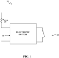
- FIG. 1 shows a block diagram of an electronic switch 11 as a switch device disclosed herein, connected in an overall electrical circuit 10 that includes a mechanical switch 12 such as a pressure switch to be sensed via the electronic switch 11.
- a mechanical switch 12 such as a pressure switch to be sensed via the electronic switch 11.
- the electronic switch 11 disclosed herein comprises an electronic switch circuit including active electronics with a current gain to sense the contact state (i.e., open or closed) of the mechanical switch 12 that is electrically coupled to the electronic switch 11.
- a high impedance mechanical contact of the mechanical switch 12 is made to appear to an external circuit 19 (external to the electronic switch 11 and the mechanical switch 12) by the electronic switch 11 as a low or constant impedance, essentially independent of contact wear in the mechanical switch.
- the result is to increase the useful life of the mechanical switch to at least a significant factor of its normal life of the mechanical switch, such as two to twenty times.
- the external circuit 19 is represented by a resistor R SENSE .
- the electronic switch 11 operates as a two-wire circuit, appearing as a purely mechanical switch would. No outside power or power connection is required. In the simplest implementation, the electronic switch 11 appears a single pole single throw switch.
- FIG. 2 shows a functional block diagram of a portion of the circuit 10 of FIG. 1 . showing the components of an embodiment of the electronic switch 11 disclosed herein, as coupled to the mechanical switch 12 to be sensed.
- the electronic switch 11 includes an electronic switch off module 13, a filter contact bounce module 14 reduces the effects of, or eliminates, contact bounce from the mechanical switch 12 and a sense open/close module 15 that senses if the mechanical switch 12 is open or closed.
- the sense module (device) 15 comprises a detection circuit allowing detection of an open or closed condition (state) of the mechanical switch 12 by causing an electronic circuit (such as a transistor, comparator, or operational amplifier), to sense a voltage that passes a threshold value. Higher than the threshold value is a first detected state of the mechanical switch, and lower than the threshold value is a second detected state of the mechanical switch.
- the switch-off module (device) 13 allows converting the detected state into an impedance change of high or low, that causes the external circuit 19 (i.e., output detection circuit) to be loaded or unloaded with respect to higher or lower current draw via the mechanical switch 12.
- One embodiment disclosed herein comprises a switching circuit 11 which includes: (1) a detection (sensor) device that senses the open or closed state of the mechanical switch, and (2) a switch-off device that in response to the sensed state of the switch, outputs a constant or low impedance indication independent of the mechanical switch contact impedance.
- One embodiment disclosed herein comprises a switching circuit including: (1) a detection device 15 that senses the open or closed state of the mechanical switch 12, and (2) a compensating circuit 13 that compensates for mechanical switch wear-out, contact damage, contact contamination and manufacturing variations in contact impedance of the mechanical switch 12.
- One embodiment of the circuit 11 comprises a sensor circuit 15 that senses the state of contact impedance of a mechanical switch 12, as an on condition when the mechanical switch is open, and an off condition when the mechanical switch is closed.
- the circuit 11 further comprises a switch-off circuit 13 that converts a sensed high impedance contact of the mechanical switch to an external circuit as a low or constant impedance.
- One embodiment of the circuit 11 comprises a sensor circuit 15 that detects an open or closed condition of a mechanical switch 12 by sensing a voltage across the mechanical electrical switch 12 passing a threshold value, wherein higher than the threshold indicates one state of the mechanical switch 12 and lower than the threshold value indicates a second state of the mechanical switch 12.
- the circuit 11 further includes a switch-off circuit 13 that represents the detected first state and second state of the mechanical switch as an impedance change of high and low, respectively.
- the output detection circuit e.g., R SENSE voltage measure
- the output detection circuit is loaded or unloaded based on the said impedance change of high or low, corresponding to higher or lower current draw via the electrical switch 12, respectively.
- FIG. 3 shows a schematic diagram of an implementation of the circuit 10 of FIG. 1 that includes an embodiment of the electronic switch 11 disclosed herein, as coupled to the mechanical switch 12.
- the implementation is one possible circuit of many that can be implemented to perform the function of the electronic switch 11.
- the electronic switch 11 comprises an electronic component with a current gain to sense the contact state (i.e., open or closed) of the mechanical switch 12 .
- a high impedance mechanical contact of the mechanical switch 12 can be made to appear to an external circuit (external to the electronic switch device and the mechanical switch, which in FIG. 3 may be as seen at the R SENSE 19 external to the switch device 11) as a low or constant impedance, essentially independent of contact wear in the mechanical switch 12.
- the switch-off module 13 of the electronic switch 11 comprises an electronic circuit comprising a transistor with high gain (e.g., greater than about 100), high Off impedance (e.g., about 10 times greater than an On condition of the transistor), and low On resistance (e.g., typically about 10 to 500 Ohms).
- the electronic switch-off module 13 comprises a current gain device 21 (e.g., bipolar transistor Q 1 type BC847CTP) and resistor 16 (e.g., a resistor R 1 ), wherein the resistor R 1 is connected in series with collector c of the transistor 21.
- a current gain device 21 e.g., bipolar transistor Q 1 type BC847CTP
- resistor 16 e.g., a resistor R 1
- the device 21 may comprise a high-reliability, no wear out electronic switch.
- the electronic device can also comprise a comparator, operational amplifier, etc.
- the device 21 puts a constant, low impedance between external circuit 19 and a power return (i.e., between SW and CC positions).
- the filter contact bounce module 14 may be optional in the electronic switch device 11.
- the filter contact bounce module 14 may include a capacitor 22 (e.g., capacitor C 2 ) and a resistor 20 (e.g., resistor R 5 ), connected in series as shown.
- the contact bounce module 14 reduces the effects of, or eliminates, contact bounce from the mechanical switch 12 as there may be some bouncing in the contacts of mechanical switch due to vibration.
- the contact bounce module 14 filters out the signals via the mechanical switch 12 that are due to bounce.
- the sense open/close module 15 includes said device 21 for sensing said contact impedance condition/state of the mechanical switch 12, as described.
- the device 21 may comprise an electronic switch of some kind, such as a transistor, general amplifier, electronic sensor, etc. This module 15 senses if the mechanical switch 12 is open or closed.
- the base terminal of the transistor device 21 is biased, via a voltage supplied, to sense the state of the mechanical switch 12 contact impedance to appear as an On condition with the mechanical switch 12 open, and Off condition with the mechanical switch 12 closed.
- a transistor device conducts current across the collector c to emitter e path, only when a voltage is applied to the base b (i.e., transistor device is On). When no base voltage is present, the transistor device functions as a switch that is Off. When base voltage is present, the transistor device functions as a switch that is On. In another example, a transistor device conducts current across the collector c to emitter e path, only when a voltage above a threshold is applied to the base b (i.e., transistor device is On). When the base voltage is less than the threshold, the transistor device functions as a switch that is Off. When the base voltage is above the threshold, the transistor device functions as a switch that is On.
- the On or Off state of the transistor device 21 is controlled with logical inverse to the closed or open position of the mechanical switch 12.
- the sensed state can be made to appear to an external circuit (e.g., R SENSE 19) as a closed or open mechanical switch 12, respectively.
- an Off state of transistor device 21 corresponds to the closed state of the mechanical switch 12
- an On state of the transistor device 21 corresponds to the open state of the mechanical switch 12, essentially independent of the contact wear, galling, fretting, contact welding, and/or contact contamination, in the mechanical switch 12.
- the electronic switch 11 may be mechanically coupled in the normally open or the normally closed state to reverse the sense logic.
- the switch 12 connection may be from the NO connection, replacing R 3 . This reverses the operational logic of the electronic switch 11 to On with switch 12 closure, and Off with switch 12 open.
- the voltage at base of the transistor 21 is about 0 Volts which turns the transistor 21 Off, and there is open circuit voltage across the transistor 21.
- the voltage drop across the resistor 18 is a high voltage determined by the resistor divider formed by resistor 18 and R SENSE , typically about 8 Volts or higher. Voltage from SW to CC is typically about 8 Volts or higher.
- the sensed voltage between SW to CC is low (e.g., typically 4 Volts) or lower when the mechanical switch 12 is open (transistor 21 is On), and high (e.g., greater than about 8 Volts) when the mechanical switch 12 is closed (transistor 21 is Off).
- the electronic switch 11 senses the voltage across the mechanical switch 12 and produces a corresponding voltage at resistor 19 which is controlled by the mechanical switch 12 being open (On) and closed (Off). This allows tailoring the electronic switch 11 for a mechanical switch 12 that has a high impedance (high contact resistance) and normally indicates a false open state for the mechanical switch 12. Coupling the electronic switch 11 between the mechanical switch 12 and the external circuit 19, eliminates effects of the false open state of mechanical switch 12 on the external circuit 19 by a gain factor of the transistor 21.
- the value of resistor 19 (R SENSE ) is about 100K Ohms and the value of the voltage V is about 28 Volts.
- the value of the resistor 18 (R 3 ) is about 140K Ohm.
- the value of the resistor 16 (R 1 ) is about 470 Ohm at 1 ⁇ 2 watt.
- the value of the resistor 20 (R 5 ) is about 1 ohm.
- the value of the resistor 17 (R 2 ) is about 1M Ohm.
- the value of capacitor 22 (C 2 ) is about at 0.022 microfarad.
- the diode 23 (D 1 ) provides a reverse polarity protection by clamping any negative voltage spike to approximately -0.7 volt.
- the resistor R 1 is connected in series with the collector c of the transistor 21.
- the resistor R 5 is connected in series between the base b of the transistor 21 and a terminal (NO) of the mechanical switch 12.
- the capacitor C 2 , the resistor R 1 , and diode D 1 are connected in parallel between the base b of the transistor 21 and ground.
- the resistor R 3 is connected between: (1) a first terminal of the resistor R 1 (and resistor R SENSE ), and a (2) first terminal of the R 5 (and to the switch 12).
- the function of the current gain at the transistor device 21 of the electronic switch 11 is to reduce the apparent contact resistance of the mechanical switch 12 by that gain factor.
- the contact impedance of the mechanical switch 12 can be made to be, e.g., about 100 times lower than the actual impedance of the mechanical switch 12.
- the voltage and current switched by the mechanical switch 12 is isolated from the external circuit 19 through the electronic switch 11 using a high resistance element 18 (e.g., resistor R 3 ) as a current limiter. This reduces the effects of welding in the mechanical switch 12. Resistor 18 limits the current that goes to the mechanical switch 12 through the electronic switch 11, which diminishes or decreases the welding contact that can occur.
- a high resistance element 18 e.g., resistor R 3
- the circuit 10 disclosed herein incorporates the action in a pressure switch which uses only a two-wire configuration.
- the electronic switch 11 can be implemented on a physical circuit board with electronic components added to the mechanical switch structure. The topology of the electronic switch 11 inverts the mechanical switch action in the basic form, as described.
- the components of the electronic switch 11 can include additional features such as contact bounce elimination by filtering in the optional module 14, as described.
- the electronic switch 11 functions as a repeater that isolates the mechanical switch 12 from a full current load and voltage extremes of the external circuit which can damage the mechanical switch 12. This reduces the effects of welding.
- the disclosed electronic separates the impedance of the mechanical switch 12 (e.g., micro-switch) through transistor 21 from the sensed impedance 16. This reduces the effects of increased impedance from galling, contact wear, fretting and welding on the mechanical micro-switch 12.
- the micro-switch 12 voltage and current load are reduced using the electronic switch 11, essentially eliminating welding effects and prolonging actual life of the micro-switch 12.
- the disclosed electronic switch 11 operates with no additional power, and the useable life of the micro-switch 12 is extended. False failures due to high impedance or contact bounce are reduced.
- the micro-switch 12 impedance characteristics can be predicted for the entire life of operation of the micro-switch 12.
- the applications of electronic switch 11 are for any mechanical switch application where wear, galling, fretting, weld damage or increasing contact impedance are issues.
- a focus for the example application described herein is in micro-switch 12 impedance sensing for pressure switches.
- a secondary application is applicability to temperature switches based on actuation of a micro-switch.
- FIG. 4 shows a schematic diagram of an alternate circuit implementation of the block diagram in FIG. 1 , that includes another embodiment of the electronic switch device 11 disclosed herein as a switch circuit 111, as coupled to the mechanical switch 12 to be sensed.
- This switch circuit 111 is similar in function to the circuit 11 in FIG. 3 using a transistor unit.
- the component 27 (U 2 ) comprises a comparator that senses a threshold voltage (similar to the transistor 21 in FIG. 3 ).
- the capacitor 30 and the resistor 31 form a contact bounce filter as in the transistor circuit in FIG. 3 .
- the diode 32 provides a reference threshold voltage
- the resistor 25 provides sense current to the mechanical switch 12.
- the resistor 28 provides voltage drive for the voltage reference diode 32.
- the resistor 31, capacitor 30 are connected in parallel with the switch 12 and the input Pin 2 of the comparator 27.
- the resistor 25 is connected in series between the collector of the switching transistor 26 and the external circuit 24.
- the resistor 28 is connected in series between the external circuit 24 and second input Pin 3 of the comparator 27.
- the resistor 29 is connected in series between the switch 12 and the external circuit 24.
- the resistor 25 (R 11 ) is about 330 Ohms
- the resistor 28 (R 14 ) is about 100K Ohm.
- a device 11 embodiment may include a sensor circuit 15 that senses the state of contact impedance of a mechanical electrical switch 12; and a switch-off circuit 13 that represents a sensed high impedance contact of the switch as a low or constant impedance.
- the switch-off circuit 13 may output a sensed high impedance contact of the switch as a low or constant impedance to an external circuit.
- the sensor circuit 15 may sense the state of contact impedance of the switch 12 when the switch is open or closed.
- the sensor circuit 15 may include a gain device 21 to sense the state of the contact impedance of the switch.
- the gain device 21 may be biased to sense the state of the contact impedance of the switch indicated as an On condition with the switch is open.
- the switch-off circuit 13 may include a gain device 21 that reduces the apparent contact resistance of the switch to an external circuit by a gain factor of the gain device.
- the gain device 21 may include a transistor device with a current gain such that the contact impedance of the switch appears lower than the sensed actual contact impedance of the switch.
- the device may further include a resistor in series with the collector of the transistor device 21, where the On or Off state of the transistor device 21, in relation to the sensed contact impedance of the switch, may be indicated to an external circuit 19 as a closed or open switch, respectively.
- the gain device 21 may include a transistor device with high gain, high Off impedance, and low On resistance.
- the sensor circuit 15 may sense a voltage, such that a sensed voltage higher than a threshold represents a first state, and a sensed voltage lower than the threshold represents a second state.
- the switch-off circuit 13 may represent the detected state into an impedance change high or low, that causes an output detection circuit 19 to be loaded or unloaded with respect to higher current draw or lower, respectively.
- the sensor circuit 15 may detect an open or closed condition of the switch 12 by sensing a voltage across the switch passing a threshold value, where higher than the threshold value indicates a first state of the switch and lower than the threshold value indicates a second state of the switch 12; and the switch-off circuit 13 may represent the detected first state and second state of the switch 12 into an impedance change of high and low, respectively, whereby the output detection circuit 19 may be loaded or unloaded based on the said impedance change of high or low, corresponding to higher or lower current draw via the electrical switch 12, respectively.
- the device may further include a filter device 14 that reduces the effects of contact bounce in electrical signals from the mechanical switch.
- a switching device 11 embodiment may include: a detection circuit 15 that may sense the open or closed state of a mechanical switch 12; and a switch-off circuit 13 that may represent the sensed open or closed state of the mechanical switch as a constant or low impedance indication, independent of the mechanical switch contact impedance.
- the detection circuit 15 may sense the state of contact impedance of the switch 12; and the switch-off circuit 13 may represent a sensed high impedance contact of the switch as a low or constant impedance.
- the sensor circuit 15 may include a gain device 21 to sense the state of the contact impedance of the switch, such that the gain device 21 is biased to sense the state of the contact impedance of the switch indicated as an On condition with the switch is open.
- the switch-off circuit 13 may include a gain device 21 that reduces the apparent contact resistance of the switch to an external circuit by a gain factor of the gain device.
- the gain device 21 may include a transistor device with a current gain such that the contact impedance of the switch appears lower than the sensed actual contact impedance of the switch.
- a switching circuit 11 embodiment may include: a detection circuit 15 that may sense contact impedance of a mechanical switch 12 for open or closed states of the mechanical switch; and a switch-off module 13 that may compensate for variations in sensed contact impedance of the mechanical switch 12, whereby the switching circuit 11.
- the switching circuit may compensate for variations in sensed contact impedance of the mechanical switch 12 due to conditions including one or more: wear-out, contact damage, contact contamination and manufacturing variations in contact impedance.
Landscapes
- Physics & Mathematics (AREA)
- General Physics & Mathematics (AREA)
- Keying Circuit Devices (AREA)
Claims (15)
- Vorrichtung (11), umfassend:einen Sensorkreis (15), der eine Verstärkungsvorrichtung (21) umfasst, die den Zustand der Kontaktimpedanz eines mechanischen elektrischen Schalters (12) erfasst; undeinen Abschaltkreis (13), der den erfassten Zustand in einen Impedanzwert konvertiert und einen erfassten hochohmigen Kontakt des Schalters (12) als niedrige oder konstante Impedanz ausgibt.
- Vorrichtung nach Anspruch 1, wobei:
der Abschaltkreis (13) einen erfassten hochohmigen Kontakt des Schalters als niedrige oder konstante Impedanz an einen externen Schaltkreis ausgibt. - Vorrichtung nach Anspruch 2, wobei:
wobei der Sensorkreis (15) den Zustand der Kontaktimpedanz des Schalters (12) erfasst, wenn der Schalter geöffnet oder geschlossen ist. - Vorrichtung nach Anspruch 1, wobei:
wobei die Verstärkungsvorrichtung (21) so vorgespannt ist, dass sie den Zustand der Kontaktimpedanz des Schalters erfasst, der als Ein-Zustand angezeigt wird, wenn der Schalter offen ist. - Vorrichtung nach Anspruch 3, wobei:
die Verstärkungsvorrichtung (21) den scheinbaren Kontaktwiderstand des Schalters gegenüber dem externen Schaltkreis um einen Verstärkungsfaktor der Verstärkungsvorrichtung reduziert. - Vorrichtung nach Anspruch 5, wobei:
die Verstärkungsvorrichtung (21) eine Transistorvorrichtung mit einer Stromverstärkung umfasst, sodass die Kontaktimpedanz des Schalters niedriger erscheint als die erfasste tatsächliche Kontaktimpedanz des Schalters. - Vorrichtung nach Anspruch 5, weiter umfassend:einen Widerstand in Reihe mit dem Kollektor der Transistorvorrichtung (21), wobei der Ein- oder Aus-Zustand der Transistorvorrichtung (21) in Bezug auf die erfasste Kontaktimpedanz des Schalters einem externen Schaltkreis (19) als ein geschlossener bzw. offener Schalter angezeigt wird; vorzugsweisewobei die Verstärkungsvorrichtung (21) eine Transistorvorrichtung mit hoher Verstärkung, hoher Aus-Impedanz und niedrigem Ein-Widerstand umfasst.
- Vorrichtung nach Anspruch 3, wobei:
wobei der Sensorkreis (15) eine Spannung erfasst, sodass eine erfasste Spannung, die höher als ein Schwellenwert ist, einen ersten Zustand darstellt, und eine erfasste Spannung, die niedriger als der Schwellenwert ist, einen zweiten Zustand darstellt. - Vorrichtung nach Anspruch 8, wobei der Abschaltkreis (13) den erfassten Zustand in eine Impedanzänderung hoch oder niedrig umsetzt, die bewirkt, dass ein Ausgangserfassungskreis (19) im Hinblick auf eine höhere bzw. niedrigere Stromaufnahme belastet oder entlastet wird.
- Vorrichtung nach Anspruch 1, wobei:wobei der Sensorkreis (15) einen offenen oder geschlossenen Zustand des Schalters (12) erfasst, indem er eine Spannung über dem Schalter erfasst, die einen Schwellenwert überschreitet, wobei ein höherer Wert als der Schwellenwert einen ersten Zustand des Schalters anzeigt und ein niedrigerer Wert als der Schwellenwert einen zweiten Zustand des Schalters (12) anzeigt; undder Abschaltkreis (13) den erfassten ersten Zustand und den zweiten Zustand des Schalters (12) in eine Impedanzänderung von hoch bzw. niedrig umsetzt,wobei der Ausgangserfassungskreis (19) auf der Grundlage der genannten Impedanzänderung von hoch oder niedrig belastet oder entlastet wird, was einer höheren bzw. niedrigeren Stromaufnahme über den elektrischen Schalter (12) entspricht.
- Vorrichtung nach Anspruch 1, weiter umfassend eine Filtervorrichtung (14), die die Auswirkungen des Kontaktprellens in elektrischen Signalen des mechanischen Schalters reduziert.
- Vorrichtung nach Anspruch 1, wobeider Sensorkreis (15) die Kontaktimpedanz des Schalters (12) für offene oder geschlossene Zustände des Schalters abtastet; undder Abschaltkreis (13) den abgetasteten offenen oder geschlossenen Zustand des Schalters als die niedrige oder konstante Impedanz darstellt, unabhängig von der Schalterkontaktimpedanz.
- Vorrichtung nach Anspruch 1, wobei die Vorrichtung Schwankungen der erfassten Kontaktimpedanz des Schalters (12) aufgrund von Bedingungen kompensiert, die eine oder mehrere der Folgenden einschließen: Abnutzung, Kontaktbeschädigung, Kontaktverschmutzung und Herstellungsschwankungen der Kontaktimpedanz.
- Vorrichtung nach Anspruch 1, wobei die Vorrichtung (11) als Zweidrahtschaltung arbeitet.
- Vorrichtung nach Anspruch 1, bei der die Verstärkungsvorrichtung (21) logisch umgekehrt zur geschlossenen oder offenen Stellung des mechanischen elektrischen Schalters (12) gesteuert wird, wobei der erfasste Zustand dem externen Schaltkreis als ein geschlossener oder offener mechanischer elektrischer Schalter (12) erscheint.
Applications Claiming Priority (2)
| Application Number | Priority Date | Filing Date | Title |
|---|---|---|---|
| US201562171178P | 2015-06-04 | 2015-06-04 | |
| PCT/US2016/035899 WO2016197052A1 (en) | 2015-06-04 | 2016-06-03 | Electronic switch |
Publications (3)
| Publication Number | Publication Date |
|---|---|
| EP3304716A1 EP3304716A1 (de) | 2018-04-11 |
| EP3304716A4 EP3304716A4 (de) | 2019-01-02 |
| EP3304716B1 true EP3304716B1 (de) | 2023-03-15 |
Family
ID=57442082
Family Applications (1)
| Application Number | Title | Priority Date | Filing Date |
|---|---|---|---|
| EP16804598.7A Active EP3304716B1 (de) | 2015-06-04 | 2016-06-03 | Elektronischer schalter |
Country Status (3)
| Country | Link |
|---|---|
| US (1) | US10677846B2 (de) |
| EP (1) | EP3304716B1 (de) |
| WO (1) | WO2016197052A1 (de) |
Families Citing this family (11)
| Publication number | Priority date | Publication date | Assignee | Title |
|---|---|---|---|---|
| JP6706236B2 (ja) * | 2016-11-07 | 2020-06-03 | 豪展醫療科技股▲ふん▼有限公司 | モードを自動的に切り替える温度測定装置及びそのモードを自動的に切り替える方法 |
| US11852131B2 (en) * | 2017-09-25 | 2023-12-26 | Carrier Corporation | Pressure safety shutoff |
| CN111426928B (zh) * | 2018-12-24 | 2021-08-20 | 东南大学 | 一种氮化镓器件动态电阻测试电路 |
| TWI685165B (zh) * | 2019-04-08 | 2020-02-11 | 大陸商東莞寶德電子有限公司 | 微動開關的訊號偵測電路與方法 |
| US11675011B2 (en) * | 2019-08-15 | 2023-06-13 | Analog Devices International Unlimited Company | Switch condition monitoring |
| JP7347006B2 (ja) * | 2019-08-28 | 2023-09-20 | 株式会社Gsユアサ | 保護装置、蓄電装置及びリレーの接点抵抗の低減方法 |
| CN110763989B (zh) * | 2019-10-29 | 2022-02-08 | 杭州中车车辆有限公司 | 一种预测城市轨道交通车辆继电器工作寿命的方法 |
| US11264193B2 (en) * | 2020-04-27 | 2022-03-01 | Hydra-Electric Company | Two wire pressure indicating switch with all electronic architecture with millivolt operating supply |
| US12586738B2 (en) * | 2021-04-01 | 2026-03-24 | Hydra-Electric Company | Electronic snubber for elimination of switch contact impedance increase and arc contaminant deposition |
| WO2024049911A2 (en) * | 2022-08-30 | 2024-03-07 | Hydra-Electric Company | Electronic snubber for elimination of switch contact impedance increase and arc contaminant deposition |
| CN117665400B (zh) * | 2023-12-05 | 2024-05-24 | 安徽农业大学 | 一种基于温度检测的开关触点接触电阻在线检测系统及方法 |
Family Cites Families (6)
| Publication number | Priority date | Publication date | Assignee | Title |
|---|---|---|---|---|
| NL9201111A (nl) * | 1992-06-24 | 1994-01-17 | Waters Beheer B V | Inrichting voor het discrimineren van de hoge en lage impedantietoestand van een schakelorgaan. |
| US5488323A (en) * | 1994-12-14 | 1996-01-30 | United Technologies Corporation | True hysteresis window comparator for use in monitoring changes in switch resistance |
| DE10043482A1 (de) | 2000-09-04 | 2002-03-14 | Infineon Technologies Ag | Current-Mode-Schaltregler |
| US7208955B2 (en) | 2005-03-15 | 2007-04-24 | Network Appliance, Inc. | Power relay or switch contact tester |
| US9148055B2 (en) | 2013-03-15 | 2015-09-29 | Cooper Technologies Company | Power system with electronic impedance switch controls and methods for supplying power to a load |
| US10042002B2 (en) * | 2014-12-12 | 2018-08-07 | Infineon Technologies Austria Ag | System and method for contact measurement circuit |
-
2016
- 2016-06-03 WO PCT/US2016/035899 patent/WO2016197052A1/en not_active Ceased
- 2016-06-03 EP EP16804598.7A patent/EP3304716B1/de active Active
- 2016-06-03 US US15/579,147 patent/US10677846B2/en active Active
Also Published As
| Publication number | Publication date |
|---|---|
| US20180172766A1 (en) | 2018-06-21 |
| US10677846B2 (en) | 2020-06-09 |
| WO2016197052A1 (en) | 2016-12-08 |
| EP3304716A1 (de) | 2018-04-11 |
| EP3304716A4 (de) | 2019-01-02 |
Similar Documents
| Publication | Publication Date | Title |
|---|---|---|
| US10677846B2 (en) | Electronic switch | |
| CN105699778B (zh) | 用于接触测量电路的系统和方法 | |
| US20090310269A1 (en) | Arrangement and method for deactivating electrical elements when malfunctioning | |
| CN110389294B (zh) | 用于实时故障检测的系统和方法 | |
| US8074961B2 (en) | Magnetic valve with manual override | |
| US20170338646A1 (en) | Device with power switch | |
| US10386403B2 (en) | Failure tolerant capacitor device | |
| US5488323A (en) | True hysteresis window comparator for use in monitoring changes in switch resistance | |
| US12306251B2 (en) | Contact-monitoring device | |
| US7781918B2 (en) | Electrical switching circuit | |
| CN110266299B (zh) | 磁性开关芯片 | |
| JP4063494B2 (ja) | 交流電源スイッチを監視する回路 | |
| CN106716156B (zh) | 电路装置和用于运行电路装置的方法 | |
| US7019532B2 (en) | Device and method for error diagnosis at digital outputs of a control module | |
| CN114256004B (zh) | 开关组件和用于测量开关组件中的触点桥的位置的方法 | |
| US10194504B2 (en) | Lighting system | |
| JP4605870B2 (ja) | タッチセンサ | |
| CN118100083B (zh) | 温升保护电路及功率开关芯片 | |
| JP6229842B2 (ja) | 過電圧保護回路 | |
| CN104781130B (zh) | 用于揭示光信号中的错误的电路装置 | |
| JP2003107123A (ja) | ダイオードの故障検出回路 | |
| US7535245B2 (en) | Integrated circuit with integrated circuit section to aid in testing | |
| CN116805564A (zh) | 具有mems继电器的开关设备 | |
| JP2006194794A (ja) | 端末機器配線の短絡検出装置 | |
| CN117476403A (zh) | 一种微机械的可电操纵的开关 |
Legal Events
| Date | Code | Title | Description |
|---|---|---|---|
| STAA | Information on the status of an ep patent application or granted ep patent |
Free format text: STATUS: THE INTERNATIONAL PUBLICATION HAS BEEN MADE |
|
| PUAI | Public reference made under article 153(3) epc to a published international application that has entered the european phase |
Free format text: ORIGINAL CODE: 0009012 |
|
| STAA | Information on the status of an ep patent application or granted ep patent |
Free format text: STATUS: REQUEST FOR EXAMINATION WAS MADE |
|
| 17P | Request for examination filed |
Effective date: 20171204 |
|
| AK | Designated contracting states |
Kind code of ref document: A1 Designated state(s): AL AT BE BG CH CY CZ DE DK EE ES FI FR GB GR HR HU IE IS IT LI LT LU LV MC MK MT NL NO PL PT RO RS SE SI SK SM TR |
|
| AX | Request for extension of the european patent |
Extension state: BA ME |
|
| DAV | Request for validation of the european patent (deleted) | ||
| DAX | Request for extension of the european patent (deleted) | ||
| A4 | Supplementary search report drawn up and despatched |
Effective date: 20181205 |
|
| RIC1 | Information provided on ipc code assigned before grant |
Ipc: H01H 9/16 20060101ALI20181127BHEP Ipc: H01H 1/00 20060101ALN20181127BHEP Ipc: H01H 35/24 20060101ALN20181127BHEP Ipc: H02M 3/156 20060101AFI20181127BHEP |
|
| STAA | Information on the status of an ep patent application or granted ep patent |
Free format text: STATUS: EXAMINATION IS IN PROGRESS |
|
| 17Q | First examination report despatched |
Effective date: 20211008 |
|
| REG | Reference to a national code |
Ref country code: DE Ref legal event code: R079 Ref document number: 602016078333 Country of ref document: DE Free format text: PREVIOUS MAIN CLASS: H02M0003156000 Ipc: H01H0009540000 |
|
| GRAP | Despatch of communication of intention to grant a patent |
Free format text: ORIGINAL CODE: EPIDOSNIGR1 |
|
| STAA | Information on the status of an ep patent application or granted ep patent |
Free format text: STATUS: GRANT OF PATENT IS INTENDED |
|
| RIC1 | Information provided on ipc code assigned before grant |
Ipc: H01H 35/24 20060101ALI20220902BHEP Ipc: H01H 1/00 20060101ALI20220902BHEP Ipc: H01H 9/16 20060101ALI20220902BHEP Ipc: G01R 31/327 20060101ALI20220902BHEP Ipc: G01R 27/20 20060101ALI20220902BHEP Ipc: H03K 17/60 20060101ALI20220902BHEP Ipc: H01H 9/54 20060101AFI20220902BHEP |
|
| INTG | Intention to grant announced |
Effective date: 20220920 |
|
| GRAS | Grant fee paid |
Free format text: ORIGINAL CODE: EPIDOSNIGR3 |
|
| GRAA | (expected) grant |
Free format text: ORIGINAL CODE: 0009210 |
|
| STAA | Information on the status of an ep patent application or granted ep patent |
Free format text: STATUS: THE PATENT HAS BEEN GRANTED |
|
| AK | Designated contracting states |
Kind code of ref document: B1 Designated state(s): AL AT BE BG CH CY CZ DE DK EE ES FI FR GB GR HR HU IE IS IT LI LT LU LV MC MK MT NL NO PL PT RO RS SE SI SK SM TR |
|
| REG | Reference to a national code |
Ref country code: CH Ref legal event code: EP Ref country code: GB Ref legal event code: FG4D |
|
| REG | Reference to a national code |
Ref country code: DE Ref legal event code: R096 Ref document number: 602016078333 Country of ref document: DE |
|
| REG | Reference to a national code |
Ref country code: IE Ref legal event code: FG4D |
|
| REG | Reference to a national code |
Ref country code: AT Ref legal event code: REF Ref document number: 1554474 Country of ref document: AT Kind code of ref document: T Effective date: 20230415 |
|
| REG | Reference to a national code |
Ref country code: LT Ref legal event code: MG9D |
|
| REG | Reference to a national code |
Ref country code: NL Ref legal event code: MP Effective date: 20230315 |
|
| PG25 | Lapsed in a contracting state [announced via postgrant information from national office to epo] |
Ref country code: RS Free format text: LAPSE BECAUSE OF FAILURE TO SUBMIT A TRANSLATION OF THE DESCRIPTION OR TO PAY THE FEE WITHIN THE PRESCRIBED TIME-LIMIT Effective date: 20230315 Ref country code: NO Free format text: LAPSE BECAUSE OF FAILURE TO SUBMIT A TRANSLATION OF THE DESCRIPTION OR TO PAY THE FEE WITHIN THE PRESCRIBED TIME-LIMIT Effective date: 20230615 Ref country code: LV Free format text: LAPSE BECAUSE OF FAILURE TO SUBMIT A TRANSLATION OF THE DESCRIPTION OR TO PAY THE FEE WITHIN THE PRESCRIBED TIME-LIMIT Effective date: 20230315 Ref country code: LT Free format text: LAPSE BECAUSE OF FAILURE TO SUBMIT A TRANSLATION OF THE DESCRIPTION OR TO PAY THE FEE WITHIN THE PRESCRIBED TIME-LIMIT Effective date: 20230315 Ref country code: HR Free format text: LAPSE BECAUSE OF FAILURE TO SUBMIT A TRANSLATION OF THE DESCRIPTION OR TO PAY THE FEE WITHIN THE PRESCRIBED TIME-LIMIT Effective date: 20230315 |
|
| REG | Reference to a national code |
Ref country code: AT Ref legal event code: MK05 Ref document number: 1554474 Country of ref document: AT Kind code of ref document: T Effective date: 20230315 |
|
| PG25 | Lapsed in a contracting state [announced via postgrant information from national office to epo] |
Ref country code: SE Free format text: LAPSE BECAUSE OF FAILURE TO SUBMIT A TRANSLATION OF THE DESCRIPTION OR TO PAY THE FEE WITHIN THE PRESCRIBED TIME-LIMIT Effective date: 20230315 Ref country code: NL Free format text: LAPSE BECAUSE OF FAILURE TO SUBMIT A TRANSLATION OF THE DESCRIPTION OR TO PAY THE FEE WITHIN THE PRESCRIBED TIME-LIMIT Effective date: 20230315 Ref country code: GR Free format text: LAPSE BECAUSE OF FAILURE TO SUBMIT A TRANSLATION OF THE DESCRIPTION OR TO PAY THE FEE WITHIN THE PRESCRIBED TIME-LIMIT Effective date: 20230616 Ref country code: FI Free format text: LAPSE BECAUSE OF FAILURE TO SUBMIT A TRANSLATION OF THE DESCRIPTION OR TO PAY THE FEE WITHIN THE PRESCRIBED TIME-LIMIT Effective date: 20230315 |
|
| PG25 | Lapsed in a contracting state [announced via postgrant information from national office to epo] |
Ref country code: SM Free format text: LAPSE BECAUSE OF FAILURE TO SUBMIT A TRANSLATION OF THE DESCRIPTION OR TO PAY THE FEE WITHIN THE PRESCRIBED TIME-LIMIT Effective date: 20230315 Ref country code: RO Free format text: LAPSE BECAUSE OF FAILURE TO SUBMIT A TRANSLATION OF THE DESCRIPTION OR TO PAY THE FEE WITHIN THE PRESCRIBED TIME-LIMIT Effective date: 20230315 Ref country code: PT Free format text: LAPSE BECAUSE OF FAILURE TO SUBMIT A TRANSLATION OF THE DESCRIPTION OR TO PAY THE FEE WITHIN THE PRESCRIBED TIME-LIMIT Effective date: 20230717 Ref country code: ES Free format text: LAPSE BECAUSE OF FAILURE TO SUBMIT A TRANSLATION OF THE DESCRIPTION OR TO PAY THE FEE WITHIN THE PRESCRIBED TIME-LIMIT Effective date: 20230315 Ref country code: EE Free format text: LAPSE BECAUSE OF FAILURE TO SUBMIT A TRANSLATION OF THE DESCRIPTION OR TO PAY THE FEE WITHIN THE PRESCRIBED TIME-LIMIT Effective date: 20230315 Ref country code: CZ Free format text: LAPSE BECAUSE OF FAILURE TO SUBMIT A TRANSLATION OF THE DESCRIPTION OR TO PAY THE FEE WITHIN THE PRESCRIBED TIME-LIMIT Effective date: 20230315 Ref country code: AT Free format text: LAPSE BECAUSE OF FAILURE TO SUBMIT A TRANSLATION OF THE DESCRIPTION OR TO PAY THE FEE WITHIN THE PRESCRIBED TIME-LIMIT Effective date: 20230315 |
|
| PG25 | Lapsed in a contracting state [announced via postgrant information from national office to epo] |
Ref country code: SK Free format text: LAPSE BECAUSE OF FAILURE TO SUBMIT A TRANSLATION OF THE DESCRIPTION OR TO PAY THE FEE WITHIN THE PRESCRIBED TIME-LIMIT Effective date: 20230315 Ref country code: PL Free format text: LAPSE BECAUSE OF FAILURE TO SUBMIT A TRANSLATION OF THE DESCRIPTION OR TO PAY THE FEE WITHIN THE PRESCRIBED TIME-LIMIT Effective date: 20230315 Ref country code: IS Free format text: LAPSE BECAUSE OF FAILURE TO SUBMIT A TRANSLATION OF THE DESCRIPTION OR TO PAY THE FEE WITHIN THE PRESCRIBED TIME-LIMIT Effective date: 20230715 |
|
| REG | Reference to a national code |
Ref country code: DE Ref legal event code: R097 Ref document number: 602016078333 Country of ref document: DE |
|
| PG25 | Lapsed in a contracting state [announced via postgrant information from national office to epo] |
Ref country code: MC Free format text: LAPSE BECAUSE OF FAILURE TO SUBMIT A TRANSLATION OF THE DESCRIPTION OR TO PAY THE FEE WITHIN THE PRESCRIBED TIME-LIMIT Effective date: 20230315 |
|
| PLBE | No opposition filed within time limit |
Free format text: ORIGINAL CODE: 0009261 |
|
| STAA | Information on the status of an ep patent application or granted ep patent |
Free format text: STATUS: NO OPPOSITION FILED WITHIN TIME LIMIT |
|
| PG25 | Lapsed in a contracting state [announced via postgrant information from national office to epo] |
Ref country code: SI Free format text: LAPSE BECAUSE OF FAILURE TO SUBMIT A TRANSLATION OF THE DESCRIPTION OR TO PAY THE FEE WITHIN THE PRESCRIBED TIME-LIMIT Effective date: 20230315 Ref country code: MC Free format text: LAPSE BECAUSE OF FAILURE TO SUBMIT A TRANSLATION OF THE DESCRIPTION OR TO PAY THE FEE WITHIN THE PRESCRIBED TIME-LIMIT Effective date: 20230315 Ref country code: DK Free format text: LAPSE BECAUSE OF FAILURE TO SUBMIT A TRANSLATION OF THE DESCRIPTION OR TO PAY THE FEE WITHIN THE PRESCRIBED TIME-LIMIT Effective date: 20230315 |
|
| REG | Reference to a national code |
Ref country code: CH Ref legal event code: PL |
|
| 26N | No opposition filed |
Effective date: 20231218 |
|
| REG | Reference to a national code |
Ref country code: BE Ref legal event code: MM Effective date: 20230630 |
|
| PG25 | Lapsed in a contracting state [announced via postgrant information from national office to epo] |
Ref country code: LU Free format text: LAPSE BECAUSE OF NON-PAYMENT OF DUE FEES Effective date: 20230603 |
|
| REG | Reference to a national code |
Ref country code: IE Ref legal event code: MM4A |
|
| PG25 | Lapsed in a contracting state [announced via postgrant information from national office to epo] |
Ref country code: LU Free format text: LAPSE BECAUSE OF NON-PAYMENT OF DUE FEES Effective date: 20230603 |
|
| PG25 | Lapsed in a contracting state [announced via postgrant information from national office to epo] |
Ref country code: IE Free format text: LAPSE BECAUSE OF NON-PAYMENT OF DUE FEES Effective date: 20230603 |
|
| PG25 | Lapsed in a contracting state [announced via postgrant information from national office to epo] |
Ref country code: IE Free format text: LAPSE BECAUSE OF NON-PAYMENT OF DUE FEES Effective date: 20230603 Ref country code: CH Free format text: LAPSE BECAUSE OF NON-PAYMENT OF DUE FEES Effective date: 20230630 |
|
| PG25 | Lapsed in a contracting state [announced via postgrant information from national office to epo] |
Ref country code: BE Free format text: LAPSE BECAUSE OF NON-PAYMENT OF DUE FEES Effective date: 20230630 |
|
| PG25 | Lapsed in a contracting state [announced via postgrant information from national office to epo] |
Ref country code: BG Free format text: LAPSE BECAUSE OF FAILURE TO SUBMIT A TRANSLATION OF THE DESCRIPTION OR TO PAY THE FEE WITHIN THE PRESCRIBED TIME-LIMIT Effective date: 20230315 |
|
| PG25 | Lapsed in a contracting state [announced via postgrant information from national office to epo] |
Ref country code: BG Free format text: LAPSE BECAUSE OF FAILURE TO SUBMIT A TRANSLATION OF THE DESCRIPTION OR TO PAY THE FEE WITHIN THE PRESCRIBED TIME-LIMIT Effective date: 20230315 |
|
| PGFP | Annual fee paid to national office [announced via postgrant information from national office to epo] |
Ref country code: DE Payment date: 20250618 Year of fee payment: 10 |
|
| PGFP | Annual fee paid to national office [announced via postgrant information from national office to epo] |
Ref country code: GB Payment date: 20250617 Year of fee payment: 10 |
|
| PGFP | Annual fee paid to national office [announced via postgrant information from national office to epo] |
Ref country code: FR Payment date: 20250617 Year of fee payment: 10 |
|
| PG25 | Lapsed in a contracting state [announced via postgrant information from national office to epo] |
Ref country code: CY Free format text: LAPSE BECAUSE OF FAILURE TO SUBMIT A TRANSLATION OF THE DESCRIPTION OR TO PAY THE FEE WITHIN THE PRESCRIBED TIME-LIMIT; INVALID AB INITIO Effective date: 20160603 |
|
| PG25 | Lapsed in a contracting state [announced via postgrant information from national office to epo] |
Ref country code: HU Free format text: LAPSE BECAUSE OF FAILURE TO SUBMIT A TRANSLATION OF THE DESCRIPTION OR TO PAY THE FEE WITHIN THE PRESCRIBED TIME-LIMIT; INVALID AB INITIO Effective date: 20160603 |
|
| PGFP | Annual fee paid to national office [announced via postgrant information from national office to epo] |
Ref country code: IT Payment date: 20250618 Year of fee payment: 10 |
|
| PG25 | Lapsed in a contracting state [announced via postgrant information from national office to epo] |
Ref country code: TR Free format text: LAPSE BECAUSE OF FAILURE TO SUBMIT A TRANSLATION OF THE DESCRIPTION OR TO PAY THE FEE WITHIN THE PRESCRIBED TIME-LIMIT Effective date: 20230315 |