EP3306679A1 - Lichtempfangendes element und optische integrierte schaltung - Google Patents
Lichtempfangendes element und optische integrierte schaltung Download PDFInfo
- Publication number
- EP3306679A1 EP3306679A1 EP16800050.3A EP16800050A EP3306679A1 EP 3306679 A1 EP3306679 A1 EP 3306679A1 EP 16800050 A EP16800050 A EP 16800050A EP 3306679 A1 EP3306679 A1 EP 3306679A1
- Authority
- EP
- European Patent Office
- Prior art keywords
- light
- receiving element
- light absorption
- absorption layer
- layer
- Prior art date
- Legal status (The legal status is an assumption and is not a legal conclusion. Google has not performed a legal analysis and makes no representation as to the accuracy of the status listed.)
- Granted
Links
Images


Classifications
-
- H—ELECTRICITY
- H10—SEMICONDUCTOR DEVICES; ELECTRIC SOLID-STATE DEVICES NOT OTHERWISE PROVIDED FOR
- H10F—INORGANIC SEMICONDUCTOR DEVICES SENSITIVE TO INFRARED RADIATION, LIGHT, ELECTROMAGNETIC RADIATION OF SHORTER WAVELENGTH OR CORPUSCULAR RADIATION
- H10F30/00—Individual radiation-sensitive semiconductor devices in which radiation controls the flow of current through the devices, e.g. photodetectors
- H10F30/20—Individual radiation-sensitive semiconductor devices in which radiation controls the flow of current through the devices, e.g. photodetectors the devices having potential barriers, e.g. phototransistors
- H10F30/21—Individual radiation-sensitive semiconductor devices in which radiation controls the flow of current through the devices, e.g. photodetectors the devices having potential barriers, e.g. phototransistors the devices being sensitive to infrared, visible or ultraviolet radiation
- H10F30/22—Individual radiation-sensitive semiconductor devices in which radiation controls the flow of current through the devices, e.g. photodetectors the devices having potential barriers, e.g. phototransistors the devices being sensitive to infrared, visible or ultraviolet radiation the devices having only one potential barrier, e.g. photodiodes
- H10F30/225—Individual radiation-sensitive semiconductor devices in which radiation controls the flow of current through the devices, e.g. photodetectors the devices having potential barriers, e.g. phototransistors the devices being sensitive to infrared, visible or ultraviolet radiation the devices having only one potential barrier, e.g. photodiodes the potential barrier working in avalanche mode, e.g. avalanche photodiodes
- H10F30/2255—Individual radiation-sensitive semiconductor devices in which radiation controls the flow of current through the devices, e.g. photodetectors the devices having potential barriers, e.g. phototransistors the devices being sensitive to infrared, visible or ultraviolet radiation the devices having only one potential barrier, e.g. photodiodes the potential barrier working in avalanche mode, e.g. avalanche photodiodes in which the active layers form heterostructures, e.g. SAM structures
-
- G—PHYSICS
- G02—OPTICS
- G02B—OPTICAL ELEMENTS, SYSTEMS OR APPARATUS
- G02B6/00—Light guides; Structural details of arrangements comprising light guides and other optical elements, e.g. couplings
- G02B6/10—Light guides; Structural details of arrangements comprising light guides and other optical elements, e.g. couplings of the optical waveguide type
- G02B6/12—Light guides; Structural details of arrangements comprising light guides and other optical elements, e.g. couplings of the optical waveguide type of the integrated circuit kind
-
- H—ELECTRICITY
- H10—SEMICONDUCTOR DEVICES; ELECTRIC SOLID-STATE DEVICES NOT OTHERWISE PROVIDED FOR
- H10F—INORGANIC SEMICONDUCTOR DEVICES SENSITIVE TO INFRARED RADIATION, LIGHT, ELECTROMAGNETIC RADIATION OF SHORTER WAVELENGTH OR CORPUSCULAR RADIATION
- H10F30/00—Individual radiation-sensitive semiconductor devices in which radiation controls the flow of current through the devices, e.g. photodetectors
- H10F30/20—Individual radiation-sensitive semiconductor devices in which radiation controls the flow of current through the devices, e.g. photodetectors the devices having potential barriers, e.g. phototransistors
- H10F30/21—Individual radiation-sensitive semiconductor devices in which radiation controls the flow of current through the devices, e.g. photodetectors the devices having potential barriers, e.g. phototransistors the devices being sensitive to infrared, visible or ultraviolet radiation
- H10F30/22—Individual radiation-sensitive semiconductor devices in which radiation controls the flow of current through the devices, e.g. photodetectors the devices having potential barriers, e.g. phototransistors the devices being sensitive to infrared, visible or ultraviolet radiation the devices having only one potential barrier, e.g. photodiodes
- H10F30/225—Individual radiation-sensitive semiconductor devices in which radiation controls the flow of current through the devices, e.g. photodetectors the devices having potential barriers, e.g. phototransistors the devices being sensitive to infrared, visible or ultraviolet radiation the devices having only one potential barrier, e.g. photodiodes the potential barrier working in avalanche mode, e.g. avalanche photodiodes
-
- H—ELECTRICITY
- H10—SEMICONDUCTOR DEVICES; ELECTRIC SOLID-STATE DEVICES NOT OTHERWISE PROVIDED FOR
- H10F—INORGANIC SEMICONDUCTOR DEVICES SENSITIVE TO INFRARED RADIATION, LIGHT, ELECTROMAGNETIC RADIATION OF SHORTER WAVELENGTH OR CORPUSCULAR RADIATION
- H10F77/00—Constructional details of devices covered by this subclass
- H10F77/10—Semiconductor bodies
- H10F77/14—Shape of semiconductor bodies; Shapes, relative sizes or dispositions of semiconductor regions within semiconductor bodies
-
- H—ELECTRICITY
- H10—SEMICONDUCTOR DEVICES; ELECTRIC SOLID-STATE DEVICES NOT OTHERWISE PROVIDED FOR
- H10F—INORGANIC SEMICONDUCTOR DEVICES SENSITIVE TO INFRARED RADIATION, LIGHT, ELECTROMAGNETIC RADIATION OF SHORTER WAVELENGTH OR CORPUSCULAR RADIATION
- H10F77/00—Constructional details of devices covered by this subclass
- H10F77/40—Optical elements or arrangements
- H10F77/413—Optical elements or arrangements directly associated or integrated with the devices, e.g. back reflectors
-
- H—ELECTRICITY
- H10—SEMICONDUCTOR DEVICES; ELECTRIC SOLID-STATE DEVICES NOT OTHERWISE PROVIDED FOR
- H10F—INORGANIC SEMICONDUCTOR DEVICES SENSITIVE TO INFRARED RADIATION, LIGHT, ELECTROMAGNETIC RADIATION OF SHORTER WAVELENGTH OR CORPUSCULAR RADIATION
- H10F10/00—Individual photovoltaic cells, e.g. solar cells
- H10F10/10—Individual photovoltaic cells, e.g. solar cells having potential barriers
- H10F10/16—Photovoltaic cells having only PN heterojunction potential barriers
-
- H—ELECTRICITY
- H10—SEMICONDUCTOR DEVICES; ELECTRIC SOLID-STATE DEVICES NOT OTHERWISE PROVIDED FOR
- H10F—INORGANIC SEMICONDUCTOR DEVICES SENSITIVE TO INFRARED RADIATION, LIGHT, ELECTROMAGNETIC RADIATION OF SHORTER WAVELENGTH OR CORPUSCULAR RADIATION
- H10F77/00—Constructional details of devices covered by this subclass
- H10F77/10—Semiconductor bodies
- H10F77/12—Active materials
- H10F77/124—Active materials comprising only Group III-V materials, e.g. GaAs
Definitions
- the present invention relates to a light-receiving element that converts an optical signal to an electrical signal, and an optical integrated circuit including the light-receiving element, and relates to, for example, a light-receiving element that makes full use of a function as an avalanche photodiode.
- a general optical receiver in optical communication is generally formed by a light-receiving element and a transimpedance amplifier (to be also referred to as a "TIA" hereinafter) that amplifies a photocurrent generated by the light-receiving element.
- TIA transimpedance amplifier
- Examples of the light-receiving element used in the optical receiver are a photodiode (to be also referred to as a "PD” hereinafter) and an avalanche photodiode (to be also referred to as an “APD” hereinafter).
- PD photodiode
- APD avalanche photodiode
- the PD has a function of converting incident light to a current.
- the upper limit of the photoelectric conversion efficiency of the PD is 100% as quantum efficiency.
- a uni-traveling carrier photodiode (UTC-PD) and the like are known in addition to a general element made of a III-V compound semiconductor such as InGaAs (see, for example, non-patent literature 1).
- the APD is a light-receiving element having a function of making photoelectrons generated in the element hit a lattice by accelerating them under a high electric field and thus ionizing the photoelectrons, thereby amplifying the carriers.
- the APD can output a plurality of carriers in correspondence with one photon, and thus obtain a sensitivity higher than 100% as the quantum conversion efficiency. For this reason, the APD is widely used for a high-sensitivity optical receiver (see, for example, non-patent literature 2).
- a waveguide type APD by silicon photonics is known.
- the waveguide type APD has the feature that an optical waveguide and a light-receiving unit can be integrated and it is unnecessary to use a spatial optical system at the time of implementation.
- non-patent literature 4 discloses an APD whose degree of integration of devices is improved by accelerating light absorption by forming a waveguide in an Si substrate and injecting a fault into the waveguide, and composing, by only Si, a material for applying an electric field in the waveguide and multiplying it.
- Non-patent literature 5 discloses a waveguide type APD in which a contact layer is provided in each waveguide having functions as a Ge light absorption layer and an Si multiplication layer and evanescent coupling is used for optical coupling between the Ge light absorption layer and the waveguide.
- the vertical incident type APD matches a CMOS process but the layer arrangement is complicated. It is thus necessary to add an enormous number of man-hours, thereby complicating the manufacturing process.
- the waveguide type APD has lower sensitivity due to the problem of optical coupling efficiency or the optical absorption coefficient of the light absorption layer, and the high gain performance and band performance cannot be simultaneously implemented because of the nonuniformity of the electric field being applied to the Si multiplication layer, thereby limiting the increase in operating speed.
- the present invention has been made in consideration of the above problems, and an object of the present invention is to easily implement a light-receiving element that serves as an APD by a monolithic manufacturing process.
- a light-receiving element that comprises a semiconductor layer including a p-type semiconductor region, an n-type semiconductor region, and a multiplication region, and a p-type light absorption layer formed on the multiplication region, wherein the p-type semiconductor region and the n-type semiconductor region are formed to sandwich the multiplication region in a planar direction of the semiconductor layer.
- Fig. 1 is a sectional view schematically showing a light-receiving element according to the first embodiment.
- a light-receiving element 10 shown in Fig. 1 has a structure in which a light absorption layer 104 is stacked on a multiplication region 103 formed between a p-type semiconductor region 101 and an n-type semiconductor region 102 in a semiconductor layer 100.
- the light-receiving element 10 includes the semiconductor layer 100, the light absorption layer 104, electrode layers 106, and insulating layers 105.
- the semiconductor layer 100 includes the p-type semiconductor region 101, the n-type semiconductor region 102, and the multiplication region 103.
- a silicon (Si) substrate or an SOI (Silicon On Insulator) substrate can be exemplified as the semiconductor layer 100.
- the p-type semiconductor region 101 and the n-type semiconductor region 102 are formed to sandwich the multiplication region 103 in the planar direction (for example, an X direction in Fig. 1 ) of the semiconductor layer 100.
- the multiplication region 103 is a region for amplifying carriers by accelerating, by the high electric field, photoelectrons moving from the light absorption layer 104. More specifically, the multiplication region 103 is a region of the semiconductor layer 100, where no impurity for forming the p-type semiconductor region 101 or the n-type semiconductor region 102 is injected. For example, when the semiconductor layer 100 is formed from the Si or SOI substrate, the multiplication region 103 is a region made of Si.
- the length in the X direction of the multiplication region 103 (the distance in the X direction between the p-type semiconductor region 101 and the n-type semiconductor region 102) is appropriately settable within a range of, for example, 20 nm to 200 nm.
- the electrode layers 106 constitute electrodes for applying voltages to the p-type semiconductor region 101 and the n-type semiconductor region 102, respectively, and are formed on the p-type semiconductor region 101 and the n-type semiconductor region 102 in the semiconductor layer 100, respectively.
- the electrode layers 106 are made of a metal material containing, for example, tungsten (W) or copper (Cu) as a main component.
- the insulating layers 105 are used to insulate the light absorption layer 104 and the electrode layers 106.
- the insulating layers 105 are made of, for example, silicon oxide (for example, SiO 2 ).
- the light absorption layer 104 is formed by selectively growing Ge on the multiplication region 103 in the semiconductor layer 100 using, as a selective growth mask, the silicon oxide layer in which the opening has been formed.
- the silicon oxide layer in which the opening has been formed For example, it is possible to selectively grow Ge on the multiplication region 103 in the semiconductor layer 100 by depositing Ge under a substrate temperature condition of 600°C by a CVD (Chemical Vapor Deposition) method using GeH 4 as a source gas.
- CVD Chemical Vapor Deposition
- Ge x Si 1-x may be grown between the Si layer and the Ge light absorption layer. In this selective growth, no Ge is deposited on the selective growth mask.
- the electrode layers 106 are formed.
- the silicon oxide layer (insulating film) deposited on the p-type semiconductor region 101 and the n-type semiconductor region 102 in the semiconductor layer 100 is selectively removed by, for example, a well-known photolithography technique and dry etching technique.
- the electrode layers 106 made of a metal material containing, for example, tungsten (W) or copper (Cu) are formed on the p-type semiconductor region 101 and the n-type semiconductor region 102 by, for example, a well-known lift-off method. More specifically, after a resist pattern used to selectively remove the silicon oxide layer is left and the metal material containing W or Cu is deposited on the semiconductor layer 100 and resist pattern, the resist pattern is removed.
- the silicon oxide layer (insulating film) between each electrode layer 106 and the light absorption layer 104 serves as the insulating layer 105.
- the light-receiving element 10 according to the first embodiment can be manufactured.
- the multiplication region 103 exhibits a multiplication function.
- the film thickness of the light absorption layer 104 is set to a size that allows the electrons and holes generated in the light absorption layer 104 to be diffused and moved to the multiplication region 103. More specifically, the film thickness of the light absorption layer 104 is set to about several hundred nm. This can move the electrons and holes generated in the light absorption layer 104 to the multiplication region 103. That is, in the light-receiving element 10 according to this embodiment, the electron-hole pairs in the light absorption layer 104 exhibit the same behavior as that of the uni-traveling carrier photodiode (UTC-PD), and the carrier transport time of the light absorption layer 104 is dominated by the electrons.
- UTC-PD uni-traveling carrier photodiode
- the light-receiving element 10 has no structure in which the light absorption layer 104 is sandwiched between electrodes (the p-type semiconductor region 101 and the n-type semiconductor region 102), unlike the conventional APD. Therefore, no electric field control layer is required, and the manufacturing process is simpler than that for the conventional vertical incident type APD or the like.
- the light-receiving element 10 has a structure in which a direction (X direction in Fig. 1 ) in which a pin junction is formed from the p-type semiconductor region 101, the multiplication region 103, and the n-type semiconductor region 102 in the semiconductor layer 100 is different from the stacking direction (Y direction in Fig. 1 ) of the light absorption layer 104 on the multiplication region 103. Therefore, an electric field when a voltage is applied between the p-type semiconductor region 101 and the n-type semiconductor region 102 almost acts on only the multiplication region 103. This can uniformly apply the electric field to the multiplication region 103.
- Fig. 5 is a sectional view schematically showing a light-receiving element according to the third embodiment.
- a semiconductor layer that has a conduction band edge located on the higher energy side with respect to the semiconductor layer forming the light absorption layer 114 and is doped into p-type conductivity is formed as the barrier layer 107 on the surface of the light absorption layer 114.
- the light absorption layer 114 is made of Si x Ge 1-x .
- the barrier layer 107 is made of, for example, Si.
- B can be exemplified.
- the band gap of the light absorption layer 114 decreases continuously or stepwise toward the interface with the semiconductor layer forming the multiplication region 103, carrier transport in the light absorption layer 114 is limited by the diffusion rate and drift velocity of electrons. At this time, all the electrons generated by light injection into the light absorption layer 114 ideally move to the multiplication region 103. However, the electrons may be diffused in a direction opposite to the multiplication region 103 (a direction opposite to the direction Y in Fig. 5 ).
- the offset of the conduction band edge between the light absorption layer 114 and the barrier layer 107 is desirably equal to or larger than 30 meV. Assuming that the light-receiving element 12 operates at room temperature, it is possible to suppress, by thermal energy, the electrons from crossing the offset of the conduction band edge between the light absorption layer 114 and the barrier layer 107, thereby contributing to further improvement of the sensitivity.
- a light-receiving element 13 shown in Fig. 7 is different from the light-receiving element 12 according to the third embodiment in that the impurity concentration of a p-type light absorption layer decreases toward a multiplication region 103 and the semiconductor layer (substrate) of the light-receiving element is made of a III-V compound semiconductor but the remaining arrangement is the same as that of the light-receiving element 12.
- the same constituent elements as those of the light-receiving element 12 according to the third embodiment are denoted by the same reference numerals and a detailed description thereof will be omitted.
- Electrode layers 106 are made of a metal material containing, for example, titanium (Ti) or gold (Au) as a main component.
- a barrier layer 107 is made of, for example, InAlAs.
- Fig. 8 is a band diagram showing a change in band gap energy in the stacking direction of the respective layers of the light-receiving element according to the fourth embodiment.
- the p-type semiconductor region 101, the n-type semiconductor region 102, and the multiplication region 103 for the light-receiving element 12 are formed in the semiconductor layer 100, and then the core 140 constituting the optical waveguide is formed on the semiconductor layer 100.
- the core 140 is formed by depositing an SiN layer on the semiconductor layer 100, and then patterning the SiN layer.
- the light absorption layer 114 is formed by selectively growing, for example, Si x Ge 1-x on the multiplication region 103 in the semiconductor layer 100 using, as a selective growth mask, the silicon oxide layer in which the opening has been formed.
- Si x Ge 1-x is selectively grown on the multiplication region 103 in the semiconductor layer 100 by a well-known CVD method or the like.
- the optical integrated circuit 20 can be manufactured.
- the optical integrated circuit 20 it is possible to implement high-quality optical coupling between the optical waveguide and the light absorption layer of the light-receiving element without departing from a normal CMOS process.
- the light absorption layer of the APD and an optical waveguide are optically coupled by evanescent coupling. Therefore, the optical coupling efficiency is insufficient and the light-receiving sensitivity of the APD is low.
- the optical integrated circuit 20 it is possible to optically couple the optical waveguide and the light absorption layer by a butt joint since the optical waveguide is formed as part of a step of forming the light-receiving element as an APD (for example, a step of forming insulating layers). This can improve the optical coupling efficiency between the optical waveguide and the light absorption layer of the light-receiving element in the optical integrated circuit 20, and improve the light-receiving sensitivity of the light-receiving element as an APD.
- APD for example, a step of forming insulating layers
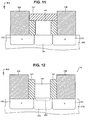
- Fig. 12 is a sectional view schematically showing a light-receiving element according to the sixth embodiment.
- a light-receiving element 14 shown in Fig. 12 is different from the light-receiving element 10 according to the first embodiment in that a light absorption layer is made of a p-type III-V compound semiconductor but the remaining arrangement is the same as that of the light-receiving element 10.
- the same constituent elements as those of the light-receiving element 10 according to the first embodiment are denoted by the same reference numerals and a detailed description thereof will be omitted.
- a semiconductor layer 100 is an Si or SOI substrate, and a multiplication region 103 is a region of the surface Si layer of the Si or SOI substrate, where no impurity is doped.
- a p-type semiconductor region 101 is formed by, for example, ion implantation of B as an impurity into the surface Si layer of the semiconductor layer 100 formed by the Si or SOI substrate.
- An n-type semiconductor region 102 is formed by, for example, ion implantation of As as an impurity into the surface Si layer of the semiconductor layer 100 formed by the Si or SOI substrate.
- Wafer bonding is performed at the initial stage of the manufacturing process of the light-receiving element. For example, after forming the p-type semiconductor region 101 and the n-type semiconductor region 102 in the Si or SOI substrate as the semiconductor layer 100, InGaAs having undergone crystal growth is bonded to the semiconductor layer 100. After bonding, similarly to the light-receiving element 10 according to the first embodiment, respective layers forming the light-receiving element are formed by a well-known photolithography technique, dry etching, and the like which are used in the normal CMOS process. This does not impair the ease of the manufacturing process even in the light-receiving element according to the sixth embodiment.
- a case has been exemplified in which the barrier layer 107 is formed on the surface of the light absorption layer 114 formed so that the band gap decreases toward the multiplication region 103 in the light-receiving element 12 according to the third embodiment.
- a barrier layer can be formed on the surface of the light absorption layer in the same manner.
- Si/SiGe, InP/InAlGaAs, and Si/InGaAs have been exemplified as combinations of materials of the multiplication region and light absorption layer as an APD.
- the present invention is not limited to them and other materials may be combined.
- Each of the first to fifth embodiments has exemplified a method of forming a light absorption layer by selectively growing it on the multiplication region 103.
- the present invention is not limited to this as long as it is possible to form a light absorption layer on the multiplication region 103.
- a light absorption layer may be formed on the multiplication region 103 by wafer bonding, chip bonding, or the like.
Landscapes
- Physics & Mathematics (AREA)
- Engineering & Computer Science (AREA)
- Microelectronics & Electronic Packaging (AREA)
- General Physics & Mathematics (AREA)
- Optics & Photonics (AREA)
- Light Receiving Elements (AREA)
Applications Claiming Priority (2)
| Application Number | Priority Date | Filing Date | Title |
|---|---|---|---|
| JP2015108575 | 2015-05-28 | ||
| PCT/JP2016/065428 WO2016190346A1 (ja) | 2015-05-28 | 2016-05-25 | 受光素子および光集積回路 |
Publications (3)
| Publication Number | Publication Date |
|---|---|
| EP3306679A1 true EP3306679A1 (de) | 2018-04-11 |
| EP3306679A4 EP3306679A4 (de) | 2018-12-19 |
| EP3306679B1 EP3306679B1 (de) | 2019-11-20 |
Family
ID=57393456
Family Applications (1)
| Application Number | Title | Priority Date | Filing Date |
|---|---|---|---|
| EP16800050.3A Active EP3306679B1 (de) | 2015-05-28 | 2016-05-25 | Lichtempfangendes element und optische integrierte schaltung |
Country Status (6)
| Country | Link |
|---|---|
| US (1) | US10199525B2 (de) |
| EP (1) | EP3306679B1 (de) |
| JP (1) | JP6480577B2 (de) |
| CN (1) | CN107615495B (de) |
| CA (1) | CA2985057C (de) |
| WO (1) | WO2016190346A1 (de) |
Families Citing this family (14)
| Publication number | Priority date | Publication date | Assignee | Title |
|---|---|---|---|---|
| JP2018148209A (ja) * | 2017-03-03 | 2018-09-20 | 住友電工デバイス・イノベーション株式会社 | 光導波路型受光素子 |
| JP6705762B2 (ja) * | 2017-03-14 | 2020-06-03 | 日本電信電話株式会社 | アバランシェフォトダイオード |
| CN109119509B (zh) * | 2017-06-23 | 2023-10-27 | 松下知识产权经营株式会社 | 光检测元件 |
| JP7059771B2 (ja) * | 2018-04-19 | 2022-04-26 | 日本電信電話株式会社 | 受光素子 |
| JP7010173B2 (ja) * | 2018-08-28 | 2022-01-26 | 日本電信電話株式会社 | 半導体受光器 |
| KR102601212B1 (ko) * | 2018-10-10 | 2023-11-10 | 삼성전자주식회사 | 광전 소자를 포함하는 집적 회로 소자 |
| US10854768B2 (en) * | 2018-12-20 | 2020-12-01 | Hewlett Packard Enterprise Development Lp | Optoelectronic component with current deflected to high-gain paths comprising an avalanche photodiode having an absorbing region on a p-doped lateral boundary, an n-doped lateral boundary and an amplifying region |
| US11309450B2 (en) | 2018-12-20 | 2022-04-19 | Analog Devices, Inc. | Hybrid semiconductor photodetector assembly |
| US11302835B2 (en) | 2019-01-08 | 2022-04-12 | Analog Devices, Inc. | Semiconductor photodetector assembly |
| JP7443672B2 (ja) | 2019-04-05 | 2024-03-06 | 富士通オプティカルコンポーネンツ株式会社 | 光半導体素子及び光伝送装置 |
| US11199672B1 (en) * | 2020-06-15 | 2021-12-14 | Globalfoundries U.S. Inc. | Multiple waveguide coupling to one or more photodetectors |
| JP7435786B2 (ja) * | 2020-07-22 | 2024-02-21 | 日本電信電話株式会社 | 受光器 |
| US12507490B2 (en) | 2021-12-29 | 2025-12-23 | Taiwan Semiconductor Manufacturing Company, Ltd. | Semiconductor device including germanium region disposed in semiconductor substrate |
| US20240347561A1 (en) * | 2022-11-10 | 2024-10-17 | The Board Of Trustees Of The University Of Arkansas | Visible to longwave infrared photodetector on silicon |
Family Cites Families (22)
| Publication number | Priority date | Publication date | Assignee | Title |
|---|---|---|---|---|
| JPS5880879A (ja) * | 1981-11-09 | 1983-05-16 | Canon Inc | 半導体素子 |
| JPS6071920A (ja) * | 1983-09-29 | 1985-04-23 | Junichi Nishizawa | 光検出器 |
| JPS6490570A (en) * | 1987-09-30 | 1989-04-07 | Shimadzu Corp | Photodiode |
| JPH03244164A (ja) * | 1990-02-22 | 1991-10-30 | Nec Corp | 半導体受光素子 |
| JP2001168372A (ja) * | 1999-12-09 | 2001-06-22 | Nippon Telegr & Teleph Corp <Ntt> | 半導体光検出器 |
| ATE401666T1 (de) | 2002-09-19 | 2008-08-15 | Quantum Semiconductor Llc | Licht-detektierende vorrichtung |
| TWI228320B (en) * | 2003-09-09 | 2005-02-21 | Ind Tech Res Inst | An avalanche photo-detector(APD) with high saturation power, high gain-bandwidth product |
| US7397101B1 (en) * | 2004-07-08 | 2008-07-08 | Luxtera, Inc. | Germanium silicon heterostructure photodetectors |
| CN100573925C (zh) * | 2005-05-18 | 2009-12-23 | 三菱电机株式会社 | 雪崩光电二极管 |
| WO2007027615A1 (en) * | 2005-09-01 | 2007-03-08 | Applied Materials, Inc. | Ridge technique for fabricating an optical detector and an optical waveguide |
| JP2010135360A (ja) * | 2008-12-02 | 2010-06-17 | Mitsubishi Electric Corp | アバランシェフォトダイオード |
| JP2010232454A (ja) * | 2009-03-27 | 2010-10-14 | Fujifilm Corp | 基板とその位置決め方法、光電変換素子とその製造方法及び製造装置、及び太陽電池 |
| JP5631668B2 (ja) * | 2010-09-02 | 2014-11-26 | Nttエレクトロニクス株式会社 | アバランシ・フォトダイオード |
| WO2012068451A2 (en) * | 2010-11-19 | 2012-05-24 | Arizona Board of Regents, a body corporate of the state of Arizona, acting for and on behalf of | Dilute sn-doped ge alloys |
| US8461624B2 (en) * | 2010-11-22 | 2013-06-11 | Intel Corporation | Monolithic three terminal photodetector |
| US8975618B2 (en) * | 2011-03-30 | 2015-03-10 | Sharp Kabushiki Kaisha | Energy conversion device with selective contacts |
| US8368159B2 (en) * | 2011-07-08 | 2013-02-05 | Excelitas Canada, Inc. | Photon counting UV-APD |
| US9780248B2 (en) * | 2012-05-05 | 2017-10-03 | Sifotonics Technologies Co., Ltd. | High performance GeSi avalanche photodiode operating beyond Ge bandgap limits |
| JP2013236012A (ja) * | 2012-05-10 | 2013-11-21 | Mitsubishi Electric Corp | アバランシェフォトダイオード及びその製造方法 |
| WO2013180690A1 (en) * | 2012-05-29 | 2013-12-05 | Hewlett-Packard Development Company, L.P. | Devices including independently controllable absorption region and multiplication region electric fields |
| JP6036197B2 (ja) * | 2012-11-13 | 2016-11-30 | 三菱電機株式会社 | アバランシェフォトダイオードの製造方法 |
| JP6879617B2 (ja) * | 2017-03-01 | 2021-06-02 | 住友電工デバイス・イノベーション株式会社 | 受光素子の製造方法 |
-
2016
- 2016-05-25 CN CN201680031131.3A patent/CN107615495B/zh active Active
- 2016-05-25 JP JP2017520735A patent/JP6480577B2/ja active Active
- 2016-05-25 WO PCT/JP2016/065428 patent/WO2016190346A1/ja not_active Ceased
- 2016-05-25 CA CA2985057A patent/CA2985057C/en active Active
- 2016-05-25 US US15/576,669 patent/US10199525B2/en active Active
- 2016-05-25 EP EP16800050.3A patent/EP3306679B1/de active Active
Also Published As
| Publication number | Publication date |
|---|---|
| CN107615495B (zh) | 2019-05-03 |
| US10199525B2 (en) | 2019-02-05 |
| EP3306679A4 (de) | 2018-12-19 |
| WO2016190346A1 (ja) | 2016-12-01 |
| JP6480577B2 (ja) | 2019-03-13 |
| CA2985057A1 (en) | 2016-12-01 |
| US20180138350A1 (en) | 2018-05-17 |
| JPWO2016190346A1 (ja) | 2017-11-16 |
| EP3306679B1 (de) | 2019-11-20 |
| CA2985057C (en) | 2019-10-22 |
| CN107615495A (zh) | 2018-01-19 |
Similar Documents
| Publication | Publication Date | Title |
|---|---|---|
| EP3306679B1 (de) | Lichtempfangendes element und optische integrierte schaltung | |
| CA2969509C (en) | Avalanche photodiode | |
| Decoster et al. | Optoelectronic sensors | |
| JP6793786B1 (ja) | 半導体受光素子、光電融合モジュール及びアバランシェフォトダイオードの製造方法 | |
| US20050051861A1 (en) | Avalanche photo-detector with high saturation power and high gain-bandwidth product | |
| EP3447806B1 (de) | Integriertes lichtempfangselement für lichtwellenleiter und verfahren zur herstellung davon | |
| CN104882509B (zh) | 一种波导对接耦合型吸收倍增分离雪崩二极管 | |
| WO2011083657A1 (ja) | アバランシェフォトダイオード及びそれを用いた受信機 | |
| US20190019903A1 (en) | SILICON WAVEGUIDE INTEGRATED WITH SILICON-GERMANIUM (Si-Ge) AVALANCHE PHOTODIODE DETECTOR | |
| CN115443546B (zh) | 一种雪崩光电二极管 | |
| US9406832B2 (en) | Waveguide-coupled MSM-type photodiode | |
| TWI686961B (zh) | 突崩式光二極體及其製造方法 | |
| Jang et al. | Metamorphic graded bandgap InGaAs-InGaAlAs-InAlAs double heterojunction PiIN photodiodes | |
| JP2001237454A (ja) | 半導体受光素子 | |
| Jang et al. | Metamorphic double heterojunction InGaAs/InGaAlAs/InAlAs photodiodes on GaAs substrates for 40 Gbit/s long wavelength optical fiber communication | |
| Achouche | InGaAs Communication Photodiodes: From low to high power level designs |
Legal Events
| Date | Code | Title | Description |
|---|---|---|---|
| STAA | Information on the status of an ep patent application or granted ep patent |
Free format text: STATUS: THE INTERNATIONAL PUBLICATION HAS BEEN MADE |
|
| PUAI | Public reference made under article 153(3) epc to a published international application that has entered the european phase |
Free format text: ORIGINAL CODE: 0009012 |
|
| STAA | Information on the status of an ep patent application or granted ep patent |
Free format text: STATUS: REQUEST FOR EXAMINATION WAS MADE |
|
| 17P | Request for examination filed |
Effective date: 20171124 |
|
| AK | Designated contracting states |
Kind code of ref document: A1 Designated state(s): AL AT BE BG CH CY CZ DE DK EE ES FI FR GB GR HR HU IE IS IT LI LT LU LV MC MK MT NL NO PL PT RO RS SE SI SK SM TR |
|
| AX | Request for extension of the european patent |
Extension state: BA ME |
|
| DAV | Request for validation of the european patent (deleted) | ||
| DAX | Request for extension of the european patent (deleted) | ||
| A4 | Supplementary search report drawn up and despatched |
Effective date: 20181120 |
|
| RIC1 | Information provided on ipc code assigned before grant |
Ipc: H01L 31/107 20060101AFI20181114BHEP Ipc: G02B 6/12 20060101ALI20181114BHEP |
|
| GRAP | Despatch of communication of intention to grant a patent |
Free format text: ORIGINAL CODE: EPIDOSNIGR1 |
|
| STAA | Information on the status of an ep patent application or granted ep patent |
Free format text: STATUS: GRANT OF PATENT IS INTENDED |
|
| INTG | Intention to grant announced |
Effective date: 20190606 |
|
| GRAA | (expected) grant |
Free format text: ORIGINAL CODE: 0009210 |
|
| STAA | Information on the status of an ep patent application or granted ep patent |
Free format text: STATUS: THE PATENT HAS BEEN GRANTED |
|
| GRAS | Grant fee paid |
Free format text: ORIGINAL CODE: EPIDOSNIGR3 |
|
| AK | Designated contracting states |
Kind code of ref document: B1 Designated state(s): AL AT BE BG CH CY CZ DE DK EE ES FI FR GB GR HR HU IE IS IT LI LT LU LV MC MK MT NL NO PL PT RO RS SE SI SK SM TR |
|
| REG | Reference to a national code |
Ref country code: GB Ref legal event code: FG4D |
|
| REG | Reference to a national code |
Ref country code: CH Ref legal event code: EP |
|
| REG | Reference to a national code |
Ref country code: IE Ref legal event code: FG4D |
|
| REG | Reference to a national code |
Ref country code: DE Ref legal event code: R096 Ref document number: 602016024793 Country of ref document: DE |
|
| REG | Reference to a national code |
Ref country code: AT Ref legal event code: REF Ref document number: 1205177 Country of ref document: AT Kind code of ref document: T Effective date: 20191215 |
|
| REG | Reference to a national code |
Ref country code: NL Ref legal event code: MP Effective date: 20191120 |
|
| REG | Reference to a national code |
Ref country code: LT Ref legal event code: MG4D |
|
| PG25 | Lapsed in a contracting state [announced via postgrant information from national office to epo] |
Ref country code: SE Free format text: LAPSE BECAUSE OF FAILURE TO SUBMIT A TRANSLATION OF THE DESCRIPTION OR TO PAY THE FEE WITHIN THE PRESCRIBED TIME-LIMIT Effective date: 20191120 Ref country code: LV Free format text: LAPSE BECAUSE OF FAILURE TO SUBMIT A TRANSLATION OF THE DESCRIPTION OR TO PAY THE FEE WITHIN THE PRESCRIBED TIME-LIMIT Effective date: 20191120 Ref country code: FI Free format text: LAPSE BECAUSE OF FAILURE TO SUBMIT A TRANSLATION OF THE DESCRIPTION OR TO PAY THE FEE WITHIN THE PRESCRIBED TIME-LIMIT Effective date: 20191120 Ref country code: BG Free format text: LAPSE BECAUSE OF FAILURE TO SUBMIT A TRANSLATION OF THE DESCRIPTION OR TO PAY THE FEE WITHIN THE PRESCRIBED TIME-LIMIT Effective date: 20200220 Ref country code: GR Free format text: LAPSE BECAUSE OF FAILURE TO SUBMIT A TRANSLATION OF THE DESCRIPTION OR TO PAY THE FEE WITHIN THE PRESCRIBED TIME-LIMIT Effective date: 20200221 Ref country code: NO Free format text: LAPSE BECAUSE OF FAILURE TO SUBMIT A TRANSLATION OF THE DESCRIPTION OR TO PAY THE FEE WITHIN THE PRESCRIBED TIME-LIMIT Effective date: 20200220 Ref country code: NL Free format text: LAPSE BECAUSE OF FAILURE TO SUBMIT A TRANSLATION OF THE DESCRIPTION OR TO PAY THE FEE WITHIN THE PRESCRIBED TIME-LIMIT Effective date: 20191120 Ref country code: LT Free format text: LAPSE BECAUSE OF FAILURE TO SUBMIT A TRANSLATION OF THE DESCRIPTION OR TO PAY THE FEE WITHIN THE PRESCRIBED TIME-LIMIT Effective date: 20191120 |
|
| PG25 | Lapsed in a contracting state [announced via postgrant information from national office to epo] |
Ref country code: HR Free format text: LAPSE BECAUSE OF FAILURE TO SUBMIT A TRANSLATION OF THE DESCRIPTION OR TO PAY THE FEE WITHIN THE PRESCRIBED TIME-LIMIT Effective date: 20191120 Ref country code: IS Free format text: LAPSE BECAUSE OF FAILURE TO SUBMIT A TRANSLATION OF THE DESCRIPTION OR TO PAY THE FEE WITHIN THE PRESCRIBED TIME-LIMIT Effective date: 20200320 Ref country code: RS Free format text: LAPSE BECAUSE OF FAILURE TO SUBMIT A TRANSLATION OF THE DESCRIPTION OR TO PAY THE FEE WITHIN THE PRESCRIBED TIME-LIMIT Effective date: 20191120 |
|
| PG25 | Lapsed in a contracting state [announced via postgrant information from national office to epo] |
Ref country code: AL Free format text: LAPSE BECAUSE OF FAILURE TO SUBMIT A TRANSLATION OF THE DESCRIPTION OR TO PAY THE FEE WITHIN THE PRESCRIBED TIME-LIMIT Effective date: 20191120 |
|
| PG25 | Lapsed in a contracting state [announced via postgrant information from national office to epo] |
Ref country code: PT Free format text: LAPSE BECAUSE OF FAILURE TO SUBMIT A TRANSLATION OF THE DESCRIPTION OR TO PAY THE FEE WITHIN THE PRESCRIBED TIME-LIMIT Effective date: 20200412 Ref country code: CZ Free format text: LAPSE BECAUSE OF FAILURE TO SUBMIT A TRANSLATION OF THE DESCRIPTION OR TO PAY THE FEE WITHIN THE PRESCRIBED TIME-LIMIT Effective date: 20191120 Ref country code: EE Free format text: LAPSE BECAUSE OF FAILURE TO SUBMIT A TRANSLATION OF THE DESCRIPTION OR TO PAY THE FEE WITHIN THE PRESCRIBED TIME-LIMIT Effective date: 20191120 Ref country code: RO Free format text: LAPSE BECAUSE OF FAILURE TO SUBMIT A TRANSLATION OF THE DESCRIPTION OR TO PAY THE FEE WITHIN THE PRESCRIBED TIME-LIMIT Effective date: 20191120 Ref country code: ES Free format text: LAPSE BECAUSE OF FAILURE TO SUBMIT A TRANSLATION OF THE DESCRIPTION OR TO PAY THE FEE WITHIN THE PRESCRIBED TIME-LIMIT Effective date: 20191120 Ref country code: DK Free format text: LAPSE BECAUSE OF FAILURE TO SUBMIT A TRANSLATION OF THE DESCRIPTION OR TO PAY THE FEE WITHIN THE PRESCRIBED TIME-LIMIT Effective date: 20191120 |
|
| REG | Reference to a national code |
Ref country code: AT Ref legal event code: MK05 Ref document number: 1205177 Country of ref document: AT Kind code of ref document: T Effective date: 20191120 |
|
| REG | Reference to a national code |
Ref country code: DE Ref legal event code: R097 Ref document number: 602016024793 Country of ref document: DE |
|
| PG25 | Lapsed in a contracting state [announced via postgrant information from national office to epo] |
Ref country code: SM Free format text: LAPSE BECAUSE OF FAILURE TO SUBMIT A TRANSLATION OF THE DESCRIPTION OR TO PAY THE FEE WITHIN THE PRESCRIBED TIME-LIMIT Effective date: 20191120 Ref country code: SK Free format text: LAPSE BECAUSE OF FAILURE TO SUBMIT A TRANSLATION OF THE DESCRIPTION OR TO PAY THE FEE WITHIN THE PRESCRIBED TIME-LIMIT Effective date: 20191120 |
|
| PLBE | No opposition filed within time limit |
Free format text: ORIGINAL CODE: 0009261 |
|
| STAA | Information on the status of an ep patent application or granted ep patent |
Free format text: STATUS: NO OPPOSITION FILED WITHIN TIME LIMIT |
|
| 26N | No opposition filed |
Effective date: 20200821 |
|
| PG25 | Lapsed in a contracting state [announced via postgrant information from national office to epo] |
Ref country code: SI Free format text: LAPSE BECAUSE OF FAILURE TO SUBMIT A TRANSLATION OF THE DESCRIPTION OR TO PAY THE FEE WITHIN THE PRESCRIBED TIME-LIMIT Effective date: 20191120 Ref country code: AT Free format text: LAPSE BECAUSE OF FAILURE TO SUBMIT A TRANSLATION OF THE DESCRIPTION OR TO PAY THE FEE WITHIN THE PRESCRIBED TIME-LIMIT Effective date: 20191120 Ref country code: PL Free format text: LAPSE BECAUSE OF FAILURE TO SUBMIT A TRANSLATION OF THE DESCRIPTION OR TO PAY THE FEE WITHIN THE PRESCRIBED TIME-LIMIT Effective date: 20191120 |
|
| PG25 | Lapsed in a contracting state [announced via postgrant information from national office to epo] |
Ref country code: IT Free format text: LAPSE BECAUSE OF FAILURE TO SUBMIT A TRANSLATION OF THE DESCRIPTION OR TO PAY THE FEE WITHIN THE PRESCRIBED TIME-LIMIT Effective date: 20191120 Ref country code: LI Free format text: LAPSE BECAUSE OF NON-PAYMENT OF DUE FEES Effective date: 20200531 Ref country code: CH Free format text: LAPSE BECAUSE OF NON-PAYMENT OF DUE FEES Effective date: 20200531 Ref country code: MC Free format text: LAPSE BECAUSE OF FAILURE TO SUBMIT A TRANSLATION OF THE DESCRIPTION OR TO PAY THE FEE WITHIN THE PRESCRIBED TIME-LIMIT Effective date: 20191120 |
|
| REG | Reference to a national code |
Ref country code: BE Ref legal event code: MM Effective date: 20200531 |
|
| GBPC | Gb: european patent ceased through non-payment of renewal fee |
Effective date: 20200525 |
|
| PG25 | Lapsed in a contracting state [announced via postgrant information from national office to epo] |
Ref country code: LU Free format text: LAPSE BECAUSE OF NON-PAYMENT OF DUE FEES Effective date: 20200525 |
|
| PG25 | Lapsed in a contracting state [announced via postgrant information from national office to epo] |
Ref country code: GB Free format text: LAPSE BECAUSE OF NON-PAYMENT OF DUE FEES Effective date: 20200525 Ref country code: IE Free format text: LAPSE BECAUSE OF NON-PAYMENT OF DUE FEES Effective date: 20200525 |
|
| PG25 | Lapsed in a contracting state [announced via postgrant information from national office to epo] |
Ref country code: BE Free format text: LAPSE BECAUSE OF NON-PAYMENT OF DUE FEES Effective date: 20200531 |
|
| PG25 | Lapsed in a contracting state [announced via postgrant information from national office to epo] |
Ref country code: TR Free format text: LAPSE BECAUSE OF FAILURE TO SUBMIT A TRANSLATION OF THE DESCRIPTION OR TO PAY THE FEE WITHIN THE PRESCRIBED TIME-LIMIT Effective date: 20191120 Ref country code: MT Free format text: LAPSE BECAUSE OF FAILURE TO SUBMIT A TRANSLATION OF THE DESCRIPTION OR TO PAY THE FEE WITHIN THE PRESCRIBED TIME-LIMIT Effective date: 20191120 Ref country code: CY Free format text: LAPSE BECAUSE OF FAILURE TO SUBMIT A TRANSLATION OF THE DESCRIPTION OR TO PAY THE FEE WITHIN THE PRESCRIBED TIME-LIMIT Effective date: 20191120 |
|
| PG25 | Lapsed in a contracting state [announced via postgrant information from national office to epo] |
Ref country code: MK Free format text: LAPSE BECAUSE OF FAILURE TO SUBMIT A TRANSLATION OF THE DESCRIPTION OR TO PAY THE FEE WITHIN THE PRESCRIBED TIME-LIMIT Effective date: 20191120 |
|
| REG | Reference to a national code |
Ref country code: DE Ref legal event code: R079 Ref document number: 602016024793 Country of ref document: DE Free format text: PREVIOUS MAIN CLASS: H01L0031107000 Ipc: H10F0030225000 |
|
| PGFP | Annual fee paid to national office [announced via postgrant information from national office to epo] |
Ref country code: DE Payment date: 20250521 Year of fee payment: 10 |
|
| PGFP | Annual fee paid to national office [announced via postgrant information from national office to epo] |
Ref country code: FR Payment date: 20250528 Year of fee payment: 10 |
|
| REG | Reference to a national code |
Ref country code: DE Ref legal event code: R081 Ref document number: 602016024793 Country of ref document: DE Owner name: NTT, INC., JP Free format text: FORMER OWNER: NIPPON TELEGRAPH AND TELEPHONE CORPORATION, TOKYO, JP Ref country code: DE Ref legal event code: R082 Ref document number: 602016024793 Country of ref document: DE Representative=s name: DENNEMEYER & ASSOCIATES RECHTSANWALTSGESELLSCH, DE |