EP3307035B1 - Procédé de fabrication d'un tableau de connexions - Google Patents
Procédé de fabrication d'un tableau de connexions Download PDFInfo
- Publication number
- EP3307035B1 EP3307035B1 EP15800707.0A EP15800707A EP3307035B1 EP 3307035 B1 EP3307035 B1 EP 3307035B1 EP 15800707 A EP15800707 A EP 15800707A EP 3307035 B1 EP3307035 B1 EP 3307035B1
- Authority
- EP
- European Patent Office
- Prior art keywords
- insulating substrate
- hole
- seed layer
- layer
- metal layer
- Prior art date
- Legal status (The legal status is an assumption and is not a legal conclusion. Google has not performed a legal analysis and makes no representation as to the accuracy of the status listed.)
- Active
Links
Images


Classifications
-
- H—ELECTRICITY
- H05—ELECTRIC TECHNIQUES NOT OTHERWISE PROVIDED FOR
- H05K—PRINTED CIRCUITS; CASINGS OR CONSTRUCTIONAL DETAILS OF ELECTRIC APPARATUS; MANUFACTURE OF ASSEMBLAGES OF ELECTRICAL COMPONENTS
- H05K3/00—Apparatus or processes for manufacturing printed circuits
- H05K3/40—Forming printed elements for providing electric connections to or between printed circuits
- H05K3/42—Plated through-holes or plated via connections
-
- H—ELECTRICITY
- H05—ELECTRIC TECHNIQUES NOT OTHERWISE PROVIDED FOR
- H05K—PRINTED CIRCUITS; CASINGS OR CONSTRUCTIONAL DETAILS OF ELECTRIC APPARATUS; MANUFACTURE OF ASSEMBLAGES OF ELECTRICAL COMPONENTS
- H05K3/00—Apparatus or processes for manufacturing printed circuits
- H05K3/40—Forming printed elements for providing electric connections to or between printed circuits
- H05K3/42—Plated through-holes or plated via connections
- H05K3/423—Plated through-holes or plated via connections characterised by electroplating method
-
- C—CHEMISTRY; METALLURGY
- C25—ELECTROLYTIC OR ELECTROPHORETIC PROCESSES; APPARATUS THEREFOR
- C25D—PROCESSES FOR THE ELECTROLYTIC OR ELECTROPHORETIC PRODUCTION OF COATINGS; ELECTROFORMING; APPARATUS THEREFOR
- C25D5/00—Electroplating characterised by the process; Pretreatment or after-treatment of workpieces
- C25D5/02—Electroplating of selected surface areas
- C25D5/022—Electroplating of selected surface areas using masking means
-
- C—CHEMISTRY; METALLURGY
- C25—ELECTROLYTIC OR ELECTROPHORETIC PROCESSES; APPARATUS THEREFOR
- C25D—PROCESSES FOR THE ELECTROLYTIC OR ELECTROPHORETIC PRODUCTION OF COATINGS; ELECTROFORMING; APPARATUS THEREFOR
- C25D5/00—Electroplating characterised by the process; Pretreatment or after-treatment of workpieces
- C25D5/48—After-treatment of electroplated surfaces
-
- C—CHEMISTRY; METALLURGY
- C25—ELECTROLYTIC OR ELECTROPHORETIC PROCESSES; APPARATUS THEREFOR
- C25D—PROCESSES FOR THE ELECTROLYTIC OR ELECTROPHORETIC PRODUCTION OF COATINGS; ELECTROFORMING; APPARATUS THEREFOR
- C25D5/00—Electroplating characterised by the process; Pretreatment or after-treatment of workpieces
- C25D5/54—Electroplating of non-metallic surfaces
-
- C—CHEMISTRY; METALLURGY
- C25—ELECTROLYTIC OR ELECTROPHORETIC PROCESSES; APPARATUS THEREFOR
- C25D—PROCESSES FOR THE ELECTROLYTIC OR ELECTROPHORETIC PRODUCTION OF COATINGS; ELECTROFORMING; APPARATUS THEREFOR
- C25D5/00—Electroplating characterised by the process; Pretreatment or after-treatment of workpieces
- C25D5/54—Electroplating of non-metallic surfaces
- C25D5/56—Electroplating of non-metallic surfaces of plastics
-
- C—CHEMISTRY; METALLURGY
- C25—ELECTROLYTIC OR ELECTROPHORETIC PROCESSES; APPARATUS THEREFOR
- C25D—PROCESSES FOR THE ELECTROLYTIC OR ELECTROPHORETIC PRODUCTION OF COATINGS; ELECTROFORMING; APPARATUS THEREFOR
- C25D7/00—Electroplating characterised by the article coated
- C25D7/12—Semiconductors
- C25D7/123—Semiconductors first coated with a seed layer or a conductive layer
-
- H—ELECTRICITY
- H05—ELECTRIC TECHNIQUES NOT OTHERWISE PROVIDED FOR
- H05K—PRINTED CIRCUITS; CASINGS OR CONSTRUCTIONAL DETAILS OF ELECTRIC APPARATUS; MANUFACTURE OF ASSEMBLAGES OF ELECTRICAL COMPONENTS
- H05K1/00—Printed circuits
- H05K1/02—Details
- H05K1/11—Printed elements for providing electric connections to or between printed circuits
- H05K1/111—Pads for surface mounting, e.g. lay-out
- H05K1/112—Pads for surface mounting, e.g. lay-out directly combined with via connections
- H05K1/113—Via provided in pad; Pad over filled via
-
- H—ELECTRICITY
- H05—ELECTRIC TECHNIQUES NOT OTHERWISE PROVIDED FOR
- H05K—PRINTED CIRCUITS; CASINGS OR CONSTRUCTIONAL DETAILS OF ELECTRIC APPARATUS; MANUFACTURE OF ASSEMBLAGES OF ELECTRICAL COMPONENTS
- H05K3/00—Apparatus or processes for manufacturing printed circuits
- H05K3/40—Forming printed elements for providing electric connections to or between printed circuits
- H05K3/42—Plated through-holes or plated via connections
- H05K3/425—Plated through-holes or plated via connections characterised by the sequence of steps for plating the through-holes or via connections in relation to the conductive pattern
- H05K3/426—Plated through-holes or plated via connections characterised by the sequence of steps for plating the through-holes or via connections in relation to the conductive pattern initial plating of through-holes in substrates without metal
-
- C—CHEMISTRY; METALLURGY
- C25—ELECTROLYTIC OR ELECTROPHORETIC PROCESSES; APPARATUS THEREFOR
- C25D—PROCESSES FOR THE ELECTROLYTIC OR ELECTROPHORETIC PRODUCTION OF COATINGS; ELECTROFORMING; APPARATUS THEREFOR
- C25D3/00—Electroplating: Baths therefor
- C25D3/02—Electroplating: Baths therefor from solutions
- C25D3/38—Electroplating: Baths therefor from solutions of copper
-
- H—ELECTRICITY
- H05—ELECTRIC TECHNIQUES NOT OTHERWISE PROVIDED FOR
- H05K—PRINTED CIRCUITS; CASINGS OR CONSTRUCTIONAL DETAILS OF ELECTRIC APPARATUS; MANUFACTURE OF ASSEMBLAGES OF ELECTRICAL COMPONENTS
- H05K2201/00—Indexing scheme relating to printed circuits covered by H05K1/00
- H05K2201/09—Shape and layout
- H05K2201/09209—Shape and layout details of conductors
- H05K2201/095—Conductive through-holes or vias
- H05K2201/09563—Metal filled via
-
- H—ELECTRICITY
- H05—ELECTRIC TECHNIQUES NOT OTHERWISE PROVIDED FOR
- H05K—PRINTED CIRCUITS; CASINGS OR CONSTRUCTIONAL DETAILS OF ELECTRIC APPARATUS; MANUFACTURE OF ASSEMBLAGES OF ELECTRICAL COMPONENTS
- H05K2203/00—Indexing scheme relating to apparatus or processes for manufacturing printed circuits covered by H05K3/00
- H05K2203/13—Moulding and encapsulation; Deposition techniques; Protective layers
- H05K2203/1377—Protective layers
- H05K2203/1383—Temporary protective insulating layer
-
- H—ELECTRICITY
- H05—ELECTRIC TECHNIQUES NOT OTHERWISE PROVIDED FOR
- H05K—PRINTED CIRCUITS; CASINGS OR CONSTRUCTIONAL DETAILS OF ELECTRIC APPARATUS; MANUFACTURE OF ASSEMBLAGES OF ELECTRICAL COMPONENTS
- H05K2203/00—Indexing scheme relating to apparatus or processes for manufacturing printed circuits covered by H05K3/00
- H05K2203/14—Related to the order of processing steps
- H05K2203/1476—Same or similar kind of process performed in phases, e.g. coarse patterning followed by fine patterning
Definitions
- the present invention relates to a process for producing a wiring board. More specifically, the present invention relates to a process for producing a wiring board which can be suitably used, for example, as a wiring board used for mounting a semiconductor chip and the like.
- a process for producing a wiring board which includes using an insulating substrate having a through hole, forming a seed layer on one surface of the insulating substrate, covering the surface of the insulating substrate opposite to the surface on which the seed layer is formed with a masking film, arranging the insulating substrate and a positive electrode so that the surface of the insulating substrate on which the seed layer is formed is faced to the positive electrode, carrying out electroplating to close the through hole existing on the surface on which the seed layer is formed with a metal layer, thereafter removing the masking film from the insulating substrate, arranging the insulating substrate and a positive electrode so that the surface of the insulating substrate from which the masking film has been removed is faced to a positive electrode, carrying out electroplating to form a metal layer in the through hole (see, for example, Patent Literature 3).
- a wiring board having high reliability can be produced because a void is hardly generated in a metal layer filled in the through hole.
- US 2015/083 469 A1 discloses a wiring board including a substrate body provided with a through hole penetrating the substrate body form one surface to another surface; and a through wiring formed in the through hole and including a first metal layer formed on a part of an inner side surface of the through hole at the one surface side, a first wiring layer that covers the first metal layer to fill a part of the through hole at the one surface side, a second metal layer continuously formed on the rest part of the inner side surface of the through hole at the other surface side and on an end portion of the first wiring layer at the other surface side, and a second wiring layer that covers the second metal layer to fill a part of the through hole at the other surface side.
- US 2013/313 122 A1 discloses a method for fabricating a conductive structure of a substrate including the steps of: providing an insulating substrate having opposite first and second surfaces and forming an insulating adhesive film on the second surface of the insulating substrate; forming at least a through hole penetrating the insulating substrate and the insulating adhesive film and forming a conductive foil on the insulating adhesive film so as to cover the through hole; and forming a shielding material on the conductive foil and the second surface of the insulating substrate and performing an electrochemical deposition process through the conductive foil so as to fill the through hole with a conductive material along a direction towards the first surface of the insulating substrate, thereby preventing the formation of voids in the through hole and hence reducing the overall resistance and preventing a blister effect from occurring.
- JP 5-558614 B1 discloses a method for manufacturing a wiring substrate using an insulating substrate having a though hole, comprising: forming a seed layer on one surface of the insulating substrate; coating a surface opposite to the surface on which the seed layer is formed with a masking film; disposing the insulating substrate and an anode so that the surface on which the seed layer of the insulating substrate is formed faces the anode and electroplating the insulating substrate; blocking a through hole on the surface on which the seed layer is formed by a metal layer and removing the masking film; and disposing the insulating film and the anode so that the surface from which the masking film was removed faces the anode and electroplating the insulating substrate to form the metal layer in through hole.
- An object of the present invention is to provide a process for producing a wiring board, which hardly generates a void in a metal layer filled in a through hole, and which enables to efficiently produce a wiring board without a process for closing a through hole existing on the surface on which a seed layer is formed with a metal layer.
- an object of the preset invention to provide a process for producing a wiring board, which hardly generates a void in a metal layer formed in a through hole, which enables to shorten a period of time necessary for plating, and enables to reduce the amount of a formed metal layer by reducing the thickness of a metal layer which is formed by electroplating on the surface of a seed layer, and which also enables to make an electrode smooth.
- the first process described thereafter is a process for producing a wiring board using an insulating substrate (1) having a through hole (2), which includes forming a seed layer (3) on one surface of the insulating substrate (1), covering the whole surface of the insulating substrate (1) on which the seed layer (3) is formed with a masking film (4), arranging the insulating substrate (1) and a positive electrode (5) so that the surface of the insulating substrate (1) which is opposite to the surface of the insulating substrate (1) on which the seed layer (3) is formed is faced to the positive electrode (5), carrying out electroplating to form a metal layer (8) in the through hole (2), and thereafter removing the masking film (4) from the insulating substrate (1).
- the aspect of the present invention is a process for producing a wiring board using an insulating substrate (1) having a through hole (2), which includes forming a seed layer (3) on one surface of the insulating substrate (1); forming a resist layer (9) on an area of the seed layer (3) where an electrode on the through hole (2) is not formed, and covering the whole surface of the insulating substrate (1) opposite to the surface of the insulating substrate (1) on which the seed layer (3) is formed with a first masking film (4); forming a first metal layer (8) in the through hole (2) by carrying out electroplating on the surface of the insulating substrate (1) on which the seed layer (3) is formed, forming a first metal layer (8) in the through hole (2) so that the diameter of an opening of the through hole (2) in which the first metal layer (8) is formed is 10 to 50% of the diameter of the opening of the through hole (2) before formation of the first metal layer (8); covering the whole surface of the insulating substrate (1) on which the seed layer (3), the resist layer (9) and the
- a void is hardly generated in a metal layer filled in a through hole, that the period of time necessary for plating can be shortened, and the amount of the formed metal can be reduced by thinning the metal layer formed on the surface of a seed layer by electroplating, and that a wiring board having a smooth electrode can be produced.
- the process for producing a wiring board of the first process is a process for producing a wiring board using an insulating substrate having a through hole, which includes forming a seed layer on one surface of the insulating substrate, covering the whole surface of the insulating substrate on which the seed layer is formed with a masking film, arranging the insulating substrate and a positive electrode so that the surface of the insulating substrate opposite to the surface of the insulating substrate on which the seed layer is formed is faced to the positive electrode, carrying out electroplating to form a metal layer in the through hole, and thereafter removing the masking film from the insulating substrate.
- a void is hardly generated in a metal layer filled in a through hole, and a wiring board can be efficiently produced without a process for closing a through hole existing on the surface of the insulating substrate on which a seed layer is formed with a metal layer.
- the process for producing a wiring board according to the invention is a process for producing a wiring board using an insulating substrate having a through hole, which includes forming a seed layer on one surface of the insulating substrate; forming a resist layer on an area of the seed layer where an electrode on the through hole is not formed, and covering the whole surface of the insulating substrate opposite to the surface of the insulating substrate on which the seed layer is formed with a first masking film; forming a first metal layer in the through hole by carrying out electroplating on the surface of the insulating substrate on which the seed layer is formed, forming a first metal layer in the through hole so that the diameter of an opening of the through hole in which the first metal layer is formed is 10 to 50% of the diameter of the opening of the through hole before formation of the first metal layer; covering the whole surface of the insulating substrate on which the seed layer, the resist layer and the first metal layer are formed with a second masking film, and removing the first masking film which covers the whole surface of the insulating substrate
- a void is hardly generated in a metal layer filled in a through hole; the period of time necessary for plating can be shortened; and the amount of the formed metal can be reduced by thinning the metal layer formed on the surface of a seed layer by electroplating; and a wiring board having a smooth electrode can be produced.
- the insulating substrate which is used in the first process and the invention has high insulating property, and that the insulating substrate is excellent in mechanical strength.
- Preferred insulating substrate includes, for example, a silicon substrate, a glass substrate, a resin substrate made of a resin such as an epoxy resin, a fluorine resin, a phenol resin, a polyester, a polyimide or a cycloolefin polymer, a substrate made of a fiber reinforced resin such as a glass fiber reinforced epoxy resin or an aramid fiber reinforced epoxy resin, and the like.
- the present invention is not limited only to those exemplified ones.
- the silicon substrate and the glass substrate are preferred because the silicon substrate and the glass substrate are excellent in handling and insulating property.
- the thickness of the insulating substrate cannot be absolutely determined, because the thickness differs depending on the use of the wiring board and the like. Therefore, it is preferred that the thickness of the insulating substrate is appropriately determined in accordance with the use of the wiring board and the like.
- the thickness of the insulating substrate is usually 30 to 800 ⁇ m or so. Also, the size of the insulating substrate cannot be absolutely determined, because the size of the insulating substrate differs depending on the use of the wiring board and the like, as well as the thickness of the insulating substrate. Therefore, it is preferred that the size of the insulating substrate is appropriately determined in accordance with the use of the wiring board and the like.
- a through hole is formed in the insulating substrate.
- the through hole can be formed in the insulating substrate, for example, by a dry etching method using plasma, a laser processing method using a laser such as an Excimer laser or a UV-YAG laser, and the like.
- the hole diameter of the through hole formed in the insulating substrate cannot be absolutely determined, because the hole diameter differs depending on the use of the wiring board and the like. Therefore, it is preferred that the hole diameter is appropriately determined in accordance with the use of the wiring board, and the like.
- the hole diameter of the through hole is preferably 1 to 200 ⁇ m, more preferably 5 to 200 ⁇ m, and furthermore preferably 10 to 100 ⁇ m from the viewpoint of inhibition of generation of a void in a metal layer formed in a through hole.
- swarf After a through hole is formed in the insulating substrate, in order to avoid that swarf, which is generated in forming a through hole by piercing the insulating substrate, remains in the through hole, it is preferred that the swarf is removed from the through hole as occasion demands.
- Fig. 1 is a schematic drawing which shows one embodiment of a process for producing a wiring board according to the first process.
- an insulating substrate 1 having a through hole 2 is used.
- a seed layer 3 is formed on one surface of the insulating substrate 1.
- the seed layer 3 is formed in order to improve adhesion of the insulating substrate 1 and a metal layer (not shown in the figure) which is described below.
- a metal is usually used as the seed layer 3.
- the metal used in the seed layer 3 is the same kind of a metal which is used in the metal layer from the viewpoint of improvement in adhesion of the glass substrate or the resin substrate, which is used as the insulating substrate 1 and the metal layer which is formed on the seed layer 3.
- the seed layer 3 is, for example, a seed layer in which a titanium layer and a copper layer are sequentially laminated from the silicon substrate side, a seed layer in which a titanium layer and a chromium layer are sequentially laminated from the silicon substrate side, a seed layer made of cobalt-tungsten-phosphorus (Co-W-P), a seed layer made of nickel-tungsten-phosphorus (Ni-W-P), or a seed layer made of palladium-cobalt-phosphorus (Pd-Co-P).
- Co-W-P cobalt-tungsten-phosphorus
- Ni-W-P nickel-tungsten-phosphorus
- Pd-Co-P palladium-cobalt-phosphorus
- the seed layer 3 can be formed, for example, by a sputtering method, a chemical vapor deposition (CVD) method, a physical vapor deposition (PVD) method, or a plating process.
- CVD chemical vapor deposition
- PVD physical vapor deposition
- the thickness of the seed layer 3 formed on one surface of the insulating substrate 1 is not particularly limited, and it is preferred that the thickness is 100 to 500 nm or so from the viewpoint of improvement in adhesion of the insulating substrate 1 and the metal layer.
- a protrusion 3a of the seed layer 3 is usually formed on the inner surface of the through hole 2 of the insulating substrate 1. Since the protrusion 3a of the seed layer 3 formed on the inner surface of the through hole 2 of the insulating substrate 1 becomes a growth point when a metal layer (not shown in the figure) is formed in the through hole 2 as described below, and enables to grow up the metal layer, a metal layer in which no void is generated can be formed.
- the length L of the protrusion 3a is preferably 10 nm or more, more preferably 20 nm or more, furthermore preferably 30 nm or more, from the viewpoint of efficient growth of the metal layer, and preferably 50 ⁇ m or less, more preferably 40 ⁇ m or less, furthermore preferably 30 ⁇ m or less, from the viewpoint of the formation of a metal layer in which no void is generated.
- the thickness D of the protrusion 3a is 3 nm or more, more preferably 5 nm or more, furthermore preferably 10 nm or more, from the viewpoint of efficient growth of the metal layer, and preferably 500 ⁇ m or less, more preferably 400 ⁇ m or less, furthermore preferably 300 ⁇ m or less, from the viewpoint of formation of a metal layer in which no void is generated.
- a masking member for preventing the formation of the seed layer 3, such as a pin (not shown in the figure) can be inserted to the through hole 2.
- the whole surface of the insulating substrate 1 on which the seed layer 3 is formed is covered with the masking film 4. Since a process for covering the surface of the insulating substrate 1 on which the seed layer 3 is formed with the masking film 4 is employed in the first process, there is not necessitated a process for closing the through hole 2 of the insulating substrate 1 by electroplating prior to filling the through hole 2 of the insulating substrate 1 with a metal layer, which has been conventionally employed, and moreover, there is not necessitated a process for closing the through hole 2 of the insulating substrate 1 by electroplating.
- the first process has an advantage in that the number of processes necessary for producing a wiring board can be significantly reduced.
- the masking film 4 includes, for example, a resin film made of a resin such as a polyester such as polyethylene terephthalate or polybutylene terephthalate; a polyolefin such as polyethylene or polypropylene; a polyamide such as nylon 11, nylon 12, nylon 6 or nylon 66; an acrylic resin such as polymethyl methacrylate; polyvinyl chloride; or polyvinylidene chloride; a film made of an elastomer such as polyurethane elastomer; a rubber sheet made of a natural rubber or a synthetic rubber such as styrene-butadiene rubber; or a metal foil such as an aluminum foil; and the first process is not limited only to those exemplified ones.
- the thickness of the masking film is not particularly limited, and it is preferred that the thickness is usually 10 to 200 ⁇ m or so.
- a process for covering the whole surface of the insulating substrate 1 on which the seed layer 3 is formed with the masking film 4 includes, for example, a process which includes using a masking film made of a thermoplastic resin as the masking film 4, placing the masking film on the whole surface of the insulating substrate 1 on which the seed layer 3 is formed, and heating the masking film for temporarily adhering the masking film to the insulating substrate 1, or a process which includes using a masking film having an adhesive layer as the masking film 4, superimposing the surface of the masking film on which the adhesive layer is formed on the surface of the insulating substrate 1 on which the seed layer 3 is formed, to temporarily adhere the masking film to the insulating substrate 1, and the first process is not limited only to those exemplified ones.
- the insulating substrate 1 and a positive electrode 5 are arranged so that the surface of the insulating substrate 1 opposite to the surface of the insulating substrate 1 on which the seed layer 3 is formed is faced to the positive electrode 5, and carrying out electroplating, to form a metal layer 8 in the through hole 2. Since the above-mentioned process is employed in the first process, there is not necessitated a process for closing the through hole 2 of the insulating substrate 1 by electroplating prior to filling the through hole 2 of the insulating substrate 1 with a metal layer, which has conventionally employed, and moreover there is not necessitated a process for closing the through hole 2 of the insulating substrate 1 by electroplating.
- the growth speed of the metal layer 8 grown up in each of through holes 2 can be controlled so as to be approximately constant, and the height of the metal layer (not shown in the figure) protruded from the through hole 2 on the surface of the insulating substrate 1 on which the seed layer 3 is formed can be controlled by the masking film 4. Therefore, there is an advantage in the process that the height of the metal layer protruded from the through hole 2 on the surface of the insulating substrate 1 on which the seed layer 3 is formed can be controlled so as to be approximately constant.
- the metal layer 8 is formed in the through hole 2 as shown in Fig. 1(e) and Fig. 1(f) .
- the metal layer 8 grows up from the seed layer 3, preferably the protrusion 3a of the seed layer 3 as a nucleus. Therefore, a metal layer 8 in which no void is generated can be formed in the through hole 2.
- an electrolysis vessel 6 can be used as shown in Fig. 1(d) .
- the insulating substrate 1 and the positive electrode 5 are arranged in an electrolysis vessel 6 so that the surface of the insulating substrate 1 opposite to the surface of the insulating substrate 1 on which the seed layer 3 covered with the masking film 4 is formed is faced to the positive electrode 5.
- the electrolysis vessel 6 is charged with a plating solution 7 so that the insulating substrate 1 and the positive electrode 5 are dipped in the plating solution 7, and then electroplating can be carried out.
- the seed layer 3 which is exposed on the surface of the through hole 2 which is opposite to the surface of the insulating substrate 1 on which the seed layer 3 is formed acts as a negative electrode.
- electrolytic plating can be carried out after the electrolysis vessel 6 is charged with the plating solution 7, and the insulating substrate 1 and the positive electrode 5 are dipped in the plating solution 7 so that the surface of the insulating substrate 1 which is opposite to the surface of the insulating substrate 1 on which the seed layer 3 is formed is faced to the positive electrode 5.
- the insulating substrate 1 and the positive electrode 5 are arranged perpendicularly (vertically).
- the insulating substrate 1 and the positive electrode 5 can be arranged horizontally.
- the distance between the insulating substrate 1 and the positive electrode 5 is not particularly limited. It is preferred that the distance is 5 to 50 mm or so from the viewpoint of efficient formation of the metal layer 8 starting from the seed layer 3 exposed on the surface of the through hole 2 which is opposite to the surface of the insulating substrate 1 on which the seed layer 3 is formed.
- the plating solution 7 can be appropriately selected in accordance with the kind of a metal which is used in a metal layer (not shown in the figure) formed in the through hole 2 of the insulating substrate 1.
- the metal which is used in the metal layer includes, for example, gold, silver, copper, platinum, aluminum, tin, rhodium, nickel, chromium, cobalt, palladium, tungsten, or an alloy made of these metals, and the first process is not limited only to those exemplified ones.
- a metal which is used in the positive electrode 5 there can be used a metal corresponding to the kind of the metal which is used in the metal layer formed in the through hole 2 of the insulating substrate 1.
- the metal which is used in the positive electrode 5 is the same as the metal which is used in the metal layer.
- the metal includes, for example, gold, silver, copper, platinum, aluminum, tin, rhodium, nickel, chromium, cobalt, palladium, tungsten, or an alloy made of these metals, and the first process is not limited only to those exemplified ones.
- the kind of the plating solution 7 can be selectively used in accordance with the kind of a metal which is used in the metal layer formed in the through hole 2 of the insulating substrate 1.
- a metal which is used in the metal layer formed in the through hole 2 of the insulating substrate 1 is copper
- the current density is not particularly limited.
- the current density is preferably 0.5 to 30 A/dm 2 , more preferably 0.5 to 5 A/dm 2 from the viewpoint of efficient formation of a close packed metal layer 8 in the through hole 2 of the insulating substrate 1.
- the liquid temperature of the plating solution 7 is not particularly limited. The liquid temperature is preferably 5 to 80°C, more preferably room temperature.
- the masking film 4 is removed from the insulating substrate 1, to give the insulating substrate 1 having the metal layer 8 which is formed and filled in the through hole 2, and the seed layer 3 on its surface, as shown in Fig. 1(g) .
- the seed layer 3 existing in the through hole 2 of the insulating substrate 1 acts as a nucleus, and the metal layer 8 successively grows up in the through hole 2 from the seed layer 3, the metal layer 8 in which no void is generated can be formed in the through hole 2. Therefore, reliability of an obtained wiring board can be remarkably enhanced.
- an electrode (not shown in the figure) can be formed on the surface 8a of the metal layer 8 as it is without a post process for smoothing the surface 8a of the metal layer 8.
- a resist layer 9 having a pattern for forming an electrode can be placed on the surface 8a of the metal layer 8 of the insulating substrate 1.
- a dry film resist is usually used as the resist layer 9 from the viewpoint of improvement in workability.
- the dry film resist includes a negative type dry film resist and a positive type dry film resist. In the first process, any of those dry film resists can be used.
- the negative type dry film resist includes, for example, a photo-curable dry film resist, or a thermosetting dry film resist, and the first process is not limited only to those exemplified ones. It is preferred that the dry film resist is previously patterned in accordance with the pattern of the insulating substrate 1.
- the thickness of the resist layer 9 is appropriately determined in accordance with the height of an electrode 10 as shown in Fig. 1(i) .
- the thickness of the resist layer 9 is usually 10 to 200 ⁇ m or so.
- the electrode 10 can be formed, for example, by electroplating.
- the electroplating can be carried out by arranging the insulating substrate 1 and a positive electrode (not shown in the figure) in an electrolysis vessel (not shown in the figure) so that the surface of the insulating substrate 1 on which the seed layer 3 is formed is faced to the positive electrode, charging the electrolysis vessel with a plating solution so that the insulating substrate 1 and the positive electrode are dipped in the plating solution, and thereafter carrying out electrolytic plating.
- the metal layer 8 filled in the through hole 2 of the insulating substrate 1 acts as a negative electrode.
- electrolytic plating also can be carried out by charging a plating vessel with a plating solution, dipping the insulating substrate 1 and the positive electrode in the plating solution so that the surface of the insulating substrate 1 on which the seed layer 3 is formed is faced to the positive electrode, and thereafter carrying out electrolytic plating.
- the distance between the insulating substrate 1 and the positive electrode is not particularly limited. It is preferred that that the distance is 5 to 50 mm or so from the viewpoint of efficient formation of the metal layer 8 starting from the metal layer 8 exposed on the surface of the insulating substrate 1 on which the seed layer 3 is formed.
- the plating solution can be appropriately selected in accordance with the kind of a metal which is used in the electrode 10.
- the metal used in the electrode 10 includes, for example, gold, silver, copper, platinum, aluminum, tin, rhodium, nickel, chromium, cobalt, palladium, tungsten, or an alloy made of these metals, and the first process is not limited only to those exemplified ones.
- a metal which is used in the positive electrode there can be used a metal corresponding to the kind of the metal which is used in the electrode 10.
- the metal which is used in the positive electrode is the same as the metal which is used in the electrode 10.
- the metal includes, for example, gold, silver, copper, platinum, aluminum, tin, rhodium, nickel, chromium, cobalt, palladium, tungsten, or an alloy made of these metals, and the first process is not limited only to those exemplified ones.
- the kind of the plating solution can be selectively used in accordance with the kind of a metal which is used in the electrode 10.
- a metal which is used in the electrode 10 is copper
- the current density is not particularly limited.
- the current density is preferably 0.5 to 30 A/dm 2 , more preferably 0.5 to 5 A/dm 2 from the viewpoint of efficient formation of a dense electrode 10.
- the liquid temperature of the plating solution 7 is not particularly limited.
- the liquid temperature is usually preferably 5 to 80°C, more preferably room temperature.
- the electrode 10 is thus formed on the surface 8a of the metal layer 8 of the insulating substrate 1.
- the thickness of the electrode 10 cannot be absolutely determined because the thickness differs depending on the use of the wiring board and the like, and the thickness is usually 3 to 80 ⁇ m or so.
- the seed layer 3 and the resist layer 9 formed on the seed layer 3 as shown in Fig. 1(i) are removed from the insulating substrate 1, to give a wiring board as shown in Fig. 1(j) .
- the resist layer 9 can be easily removed from the insulating substrate 1, for example, by exfoliating.
- the seed layer 3 can be easily removed from the insulating substrate 1, for example, by chemical reaction with a wet etching technique in which an etchant (etching solution) is used.
- the wiring board can be efficiently produced without a process for closing the through hole on the surface of the insulating substrate 1 on which the seed layer is formed with a metal layer.
- the wiring board obtained by the process for producing a wiring board of the first invention is excellent in reliability since a void is hardly generated in the metal layer filled in the through hole. Therefore, it is expected that the wiring board is used, for example, as a wiring board for mounting a semiconductor chip.
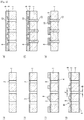
- FIG. 2 is a schematic drawing which shows one embodiment of a process for producing a wiring board according to the invention.
- an insulating substrate 1 having a through hole 2 is used.
- a seed layer 3 is formed on one surface of the insulating substrate 1.
- the seed layer 3 is formed in order to improve the adhesion of the insulating substrate 1 and a metal which is used in electroplating.
- a metal is usually used.
- the metal which is used in the seed layer 3 is the same kind as the metal which is used in electroplating from the viewpoint of improvement in adhesion of the glass substrate or the resin substrate which is used as the insulating substrate 1 and the metal layer (not shown in the figure) which is formed on the seed layer 3.
- the seed layer 3 is, for example, a seed layer in which a titanium layer and a copper layer are sequentially laminated from the silicon substrate side, a seed layer in which a titanium layer and a chromium layer are sequentially laminated from the silicon substrate side, a seed layer made of cobalt-tungsten-phosphorus (Co-W-P), a seed layer made of nickel-tungsten-phosphorus (Ni-W-P), or a seed layer made of palladium-cobalt-phosphorus (Pd-Co-P).
- Co-W-P cobalt-tungsten-phosphorus
- Ni-W-P nickel-tungsten-phosphorus
- Pd-Co-P palladium-cobalt-phosphorus
- the seed layer 3 can be formed, for example, by a sputtering method, a chemical vapor deposition (CVD) method, a physical vapor deposition (PVD) method, or a plating process.
- CVD chemical vapor deposition
- PVD physical vapor deposition
- the thickness of the seed layer 3 which is formed on one surface of the insulating substrate 1 is not particularly limited, and it is preferred that the thickness is 100 to 500 nm or so from the viewpoint of improvement in adhesion of the insulating substrate 1 and the metal which is used in electroplating.
- a part of the seed layer 3 is sometimes formed on the inner surface of the through hole 2 of the insulating substrate 1.
- a part of the seed layer 3 can be formed on the inner surface of the through hole 2 of the insulating substrate 1, or the seed layer 3 can be formed only on the surface of the insulating substrate 1, so long as an object of the invention is not hindered.
- a masking member such as a pin (not shown in the figure) for preventing the formation of a seed layer 3 on the inner surface can be inserted to the through hole 2.
- a resist layer 9 is formed on an area of the seed layer (3) which is formed in the above where an electrode on the through hole is not formed (not shown in the figure), and the whole surface of the insulating substrate 1 which is opposite to the surface of the insulating substrate 1 on which the seed layer 3 is formed is covered with a first masking film 4.
- the order of a process for forming the resist layer 9 on an area of the seed layer 3 where an electrode on the through hole is not formed and a process for covering the whole surface of the insulating substrate 1 which is opposite to the surface of the insulating substrate 1 on which the seed layer 3 is formed with the first masking film 4 is not particularly limited, and any of these operations can be carried out earlier.
- the area of the seed layer 3 where an electrode on the through hole is not formed means an area where the electrode 10 is not formed on the seed layer 3 as shown in Fig. 2(g) .
- the electrode 10 is usually formed on the through hole 2.
- a dry film resist is usually used as the resist layer 9 from the viewpoint of improvement in workability.
- the dry film resist includes a negative type dry film resist and a positive type dry film resist. In the invention, any of those dry film resists can be used.
- the negative type dry film resist includes, for example, a photo-curable dry film resist, or a thermosetting dry film resist, and the invention is not limited only to those exemplified ones. It is preferred that the dry film resist is previously patterned in accordance with the pattern of the insulating substrate 1.
- the thickness of the resist layer 9 is appropriately determined in accordance with the height of the electrode 10 as shown in Fig. 2(g) .
- the thickness of the resist layer 9 is usually 10 to 200 ⁇ m or so.
- the whole surface of the insulating substrate 1 which is opposite to the surface of the insulating substrate 1 on which the seed layer 3 is formed is covered with a first masking film 4.
- the first masking film 4 includes, for example, a resin film made of a resin such as a polyester such as polyethylene terephthalate or polybutylene terephthalate; a polyolefin such as polyethylene or polypropylene; a polyamide such as nylon 11, nylon 12, nylon 6 or nylon 66; an acrylic resin such as polymethyl methacrylate; polyvinyl chloride; or polyvinylidene chloride; a film made of an elastomer such as polyurethane elastomer; a rubber sheet made of a natural rubber or a synthetic rubber such as styrene-butadiene rubber; or a metal foil such as an aluminum foil; and the invention is not limited only to those exemplified ones.
- the thickness of the first masking film is not particularly limited, and it is preferred that the thickness is
- a process for covering the whole surface of the insulating substrate 1 opposite to the surface of the insulating substrate 1 on which the seed layer 3 is formed with the first masking film 4 includes, for example, a process which includes using a first masking film made of a thermoplastic resin as the masking film 4, placing the first masking film on the whole surface of the insulating substrate 1 which is opposite to the surface of the insulating substrate 1 on which the seed layer 3 is formed, and heating the first masking film for temporarily adhering the first masking film to the insulating substrate 1, or a process which includes using a first masking film having an adhesive layer as the first masking film 4, superimposing the surface of the first masking film on which the adhesive layer is formed on the surface of the insulating substrate 1 which is opposite to the surface of the insulating substrate 1 on which the seed layer 3 is formed, to temporarily adhere the masking film to the insulating substrate 1, and the invention is not limited only to those exemplified ones.
- a first metal layer 8 is formed in the through hole 2 by carrying out electroplating on the surface of the insulating substrate 1 on which the seed layer 3 is formed, the first metal layer 8 is formed in the through hole 2 so that the diameter of the opening of the through hole 2 in which the first metal layer 8 is formed is 10 to 50% of the diameter of the opening of the through hole 2 before the formation of the first metal layer 8, as shown in Fig. 2(d) .
- the first metal layer 8 is formed on the seed layer 3.
- the first metal layer 8 is formed on the entire surface of the seed layer 3. Therefore, as shown in Fig. 2(d) , a through hole 11 having a diameter d which becomes gradually smaller is formed.
- the diameter d of the opening of the through hole 11 is controlled so as to be 10 to 50% of the diameter D of the opening of the through hole 2 before the formation of the first metal layer 8 (initial stage).
- the diameter d of the opening of the through hole 11 in which the first metal layer 8 is formed is controlled so that the value determined by the equation: (diameter d/diameter D) ⁇ 100 becomes 10 to 50%.
- a process for controlling the diameter d of the opening of the through hole 11 to 10 to 50% of the diameter D of the opening of the through hole 2 before the formation of the first metal layer 8 is employed. Since the above-mentioned process is employed in the invention, there are exhibited excellent effects such that a void is hardly generated in the second metal layer 13 which is formed in the through hole 2.
- the process for carrying out electroplating on the seed layer 3 includes, for example, a process which includes arranging the insulating substrate 1 and a positive electrode (not shown in the figure) so that the surface of the insulating substrate 1 on which the seed layer 3 is formed is faced to the positive electrode, and carrying out electroplating on the seed layer 3.
- a first metal layer 8 precipitates from the seed layer 3 as a starting point, and the diameter d of the opening of the through hole 2 gradually becomes smaller.
- the first metal layer 8 is formed until the diameter d of the opening of the through hole 11 becomes 10 to 50% of the diameter D of the opening of the through hole 2 before the formation of the first metal layer 8.
- an electrolysis vessel (not shown in the figure) can be used.
- the insulating substrate 1 and a positive electrode (not shown in the figure) are arranged in the electrolysis vessel so that the surface of the insulating substrate 1 on which the seed layer 3 is formed is faced to the positive electrode, and the electrolysis vessel is charged with a plating solution so that the insulating substrate 1 and the positive electrode are dipped in the plating solution. Thereafter, electroplating can be carried out. At that time, the surface of the insulating substrate 1 on which the seed layer 3 is formed acts as a negative electrode.
- the electroplating also can be carried out after the electrolysis vessel is charged with a plating solution, and then the insulating substrate 1 and the positive electrode are dipped in the plating solution.
- the distance between the insulating substrate 1 and the positive electrode is not particularly limited, and it is preferred that the distance is 5 to 50 mm or so from the viewpoint that electroplating is carried out efficiently on the surface of the insulating substrate 1 on which the seed layer 3 is formed.
- the plating solution can be appropriately selectively used in accordance with the kind of a first metal layer 8 which is formed in the through hole 2 of the insulating substrate 1.
- the metal which is used in the first metal layer 8 includes, for example, gold, silver, copper, platinum, aluminum, tin, rhodium, nickel, chromium, cobalt, palladium, tungsten, or an alloy made of these metals, and the invention is not limited only to those exemplified ones.
- a metal which is used in the positive electrode there can be used a metal corresponding to the kind of the metal which is used in the first metal layer 8 formed in the through hole 2 of the insulating substrate 1.
- the metal which is used in the positive electrode is the same as the metal which is formed in the through hole 2 of the insulating substrate 1.
- the above-mentioned metal includes, for example, gold, silver, copper, platinum, aluminum, tin, rhodium, nickel, chromium, cobalt, palladium, tungsten, or an alloy made of these metals, and the invention is not limited only to those exemplified ones.
- the kind of the plating solution can be selectively used in accordance with the kind of a metal which is used in the first metal layer 8 formed in the through hole 2 of the insulating substrate 1.
- a metal which is used in the first metal layer 8 formed in the through hole 2 of the insulating substrate 1 is copper
- the current density is not particularly limited.
- the current density is preferably 0.5 to 10 A/dm 2 , more preferably 0.5 to 5 A/dm 2 from the viewpoint of efficient formation of a close packed first metal layer 8 in the through hole 2 of the insulating substrate 1.
- the liquid temperature of the plating solution is not particularly limited. The liquid temperature is usually preferably 5 to 80°C, more preferably 10 to 60°C, furthermore preferably room temperature.
- the whole surface of the insulating substrate 1 on which the seed layer 3, the resist layer 9 and the first metal layer 8 are formed is covered with a second masking film 12, and the first masking film 4 which covers the whole surface of the insulating substrate 1 opposite to the surface of the insulating substrate 1 on which the seed layer 3 is formed is removed from the insulating substrate 1.
- the order of carrying out a process for covering the whole surface of the insulating substrate 1 on which the seed layer 3, the first resist layer 9 and the first metal layer 8 are formed with the second masking film 12 and a process for removing the first masking film 4 which covers the whole surface of the insulating substrate 1 opposite to the surface of the insulating substrate 1 on which the seed layer 3 is formed is not particularly limited, and any of these operations can be carried out earlier.
- the masking film 12 includes, for example, a resin film made of a resin such as a polyester such as polyethylene terephthalate or polybutylene terephthalate; a polyolefin such as polyethylene or polypropylene; a polyamide such as nylon 11, nylon 12, nylon 6 or nylon 66; an acrylic resin such as polymethyl methacrylate; polyvinyl chloride; or polyvinylidene chloride; a film made of an elastomer such as polyurethane elastomer; a rubber sheet made of a natural rubber or a synthetic rubber such as styrene-butadiene rubber; or a metal foil such as an aluminum foil, and the invention is not limited only to those exemplified ones.
- the thickness of the masking film is not particularly limited, and it is preferred that the thickness is usually 10 to 200 ⁇ m or so.
- the process for covering the whole surface of the insulating substrate 1 on which the seed layer 3, the resist layer 9 and the first metal layer 8 of the insulating substrate 1, are formed with the second masking film 12 includes, for example, a process which includes using a masking film made of a thermoplastic resin as the second masking film 12, placing the second masking film on the surface of the insulating substrate 1 on which the seed layer 3, the resist layer 9 and the first metal layer 8 are formed, and heating the masking film for temporarily adhering the second masking film to the insulating substrate 1, or a process which includes using a masking film having an adhesive layer as the second masking film 12, superimposing the surface of the masking film on which the adhesive layer is formed on the surface of the insulating substrate 1 on which the seed layer 3 is formed, to temporarily adhere the masking film 4 to the insulating substrate 1, and the invention is not limited only to those exemplified ones.
- the seed layer 3 can be contacted with the second masking film 12 by thinning the resist layer 9 so as not to form the space between the first metal layer 8 and the second masking film 12.
- electroplating is carried out from the surface of the insulating substrate 1 opposite to the surface of the insulating substrate 1 on which the seed layer 3 is formed, to form a secondmetal layer 13 in the through hole 2.
- a process for carrying out electroplating on the surface of the insulating substrate 1 opposite to the surface of the insulating substrate on which the seed layer 3 is formed includes, for example, a process for arranging the insulating substrate 1 and a positive electrode (not shown in the figure) so that the surface of the insulating substrate 1 opposite to the surface of the insulating substrate 1 on which the seed layer 3 is formed is faced to the positive electrode, and carrying out electroplating on the surface of the insulating substrate 1 opposite to the surface on which the seed layer 3 is formed.
- an electrolysis vessel (not shown in the figure) can be used in the same manner as mentioned above.
- the insulating substrate 1 and a positive electrode (not shown in the figure) are arranged in an electrolysis vessel so that the surface of the insulating substrate 1 opposite to the surface of the insulating substrate 1 on which the seed layer 3 is formed is faced to the positive electrode, and the electrolysis vessel is charged with a plating solution so that the insulating substrate 1 and the positive electrode are dipped in the plating solution. Thereafter, electroplating can be carried out.
- the seed layer 3 of the insulating substrate 1 acts as a negative electrode.
- the electroplating also can be carried out after the electrolysis vessel is charged with a plating solution, and then the insulating substrate 1 and the positive electrode are dipped in the plating solution.
- the distance between the surface of the insulating substrate 1 opposite to the surface of the insulating substrate 1 on which the seed layer 3 is formed and the positive electrode is not particularly limited, and the distance is preferably 5 to 50 mm or so from the viewpoint that electroplating can be efficiently carried out from the surface of the insulating substrate 1 opposite to the surface of the insulating substrate 1 on which the seed layer 3 is formed.
- the plating solution can be appropriately selectively used in accordance with the kind of a metal which is used in the second metal layer 13 formed in the through hole 2 of the insulating substrate 1.
- the metal which is used in the second metal layer 13 includes, for example, gold, silver, copper, platinum, aluminum, tin, rhodium, nickel, chromium, cobalt, palladium, tungsten, or an alloy made of these metals, and the invention is not limited only to those exemplified ones.
- a metal which is used in the positive electrode there can be used a metal corresponding to the kind of the metal which is used in the second metal layer 13 formed in the through hole 2 of the insulating substrate 1.
- the metal which is used in the positive electrode is the same as the metal which is formed in the through hole 2 of the insulating substrate 1.
- the above-mentioned metal includes, for example, gold, silver, copper, platinum, aluminum, tin, rhodium, nickel, chromium, cobalt, palladium, tungsten, or an alloy made of these metals, and the invention is not limited only to those exemplified ones.
- the kind of the plating solution can be selectively used in accordance with the kind of a metal which is used in the second metal layer 13 formed in the through hole 2 of the insulating substrate 1 in the same manner as mentioned above.
- a metal which is used in the second metal layer 13 formed in the through hole 2 of the insulating substrate 1 is copper
- the current density is not particularly limited.
- the current density is preferably 0.5 to 10 A/dm 2 , more preferably 0.5 to 5 A/dm 2 from the viewpoint of efficient formation of a close packed second metal layer 13 in the through hole 2 of the insulating substrate 1.
- the liquid temperature of the plating solution is not particularly limited. The liquid temperature is preferably 5 to 80°C, more preferably 10 to 60°C, furthermore preferably room temperature.
- the electroplating is thus carried out from the surface of the insulating substrate 1 opposite to the surface of the insulating substrate 1 on which the seed layer 3 is formed to form a second metal layer 13 in the through hole 2, and thereby an electrode 10 can be formed.
- the second masking film 12, the resist layer 9 and the seed layer 3 are removed from the insulating substrate 1, to give a wiring board as shown in Fig. 2(g) .
- the seed layer remaining on the insulating substrate 1 can be easily removed from the insulating substrate 1, for example, by chemical reaction with a wet etching technique in which an etchant (etching solution) is used.
- etching solution etching solution
- the wiring board can be produced by the process as described above. According to the process for producing a wiring board of the invention, since a void is hardly generated, reliability of a wiring board is significantly improved. Moreover, since the thickness of a metal formed by electroplating on the surface of the seed layer can be reduced, the period of time necessary for plating can be shortened, the amount of a metal which is used in an electrode can be reduced, and a wiring board having an electrode of which surface is smooth can be produced.
- a wiring board of the invention there is no necessity to provide a wiring board with an electrode after the production of a wiring board, which has been conventionally necessitated. Since a metal layer is formed in the through hole of an insulating substrate under the condition such that a masking film is placed on the seed layer, an electrode having a smooth surface can be formed. Therefore, a wiring board having an electrode of which surface is smooth can be efficiently produced.
- a metal layer grows up from each through hole existing on both surfaces of the insulating substrate to the central portion of the insulating substrate in thickness. Therefore, in accordance with the formation of a metal layer in the through hole, the concentration of a metal contained in a plating solution is gradually lowered, and a current density of the plating solution is gradually lowered. Thereby, not only production efficiency of a wiring board is lowered, but also a void is easily generated in the central portion of the through hole.
- a process for producing a wiring board of the invention when a first metal layer is formed in the through hole by carrying out electroplating on the surface of the insulating substrate on which the seed layer is formed, there is employed a process for forming a first metal layer in the through hole so that the diameter of the opening of the through hole in which the first metal layer is formed is 10 to 50% of the diameter of the opening of the through hole before the formation of the first metal layer, and carrying out electroplating from the surface of the insulating substrate opposite to the surface of the insulating substrate on which the seed layer is formed, to form a second metal layer in the through hole.
- a void is hardly generated in a second metal layer which is formed in a through hole; the thickness of a metal formed on the surface of the seed layer by electroplating can be reduced; the period of time necessary for plating can be shortened; the amount of a metal which is used in a first metal layer can be reduced; and a wiring board having an electrode of which surface is smooth can be produced.
- the wiring board is excellent in reliability. Therefore, the wiring board is expected to be used, for example, as a wiring board for mounting a semiconductor chip, and the like.
- a silicon substrate having a diameter of 150 mm and a thickness of 300 ⁇ m, provided with 50 through holes having a hole diameter of 50 ⁇ m on a straight line aligned at a regular interval of 500 ⁇ m.
- a titanium layer having a thickness of 50 nm was formed as a seed layer on one surface of the silicon substrate, and then a copper layer having a thickness of 300 nm was formed on the surface by using a load-lock type sputtering apparatus commercially available from ULVAC, Inc. under the model number of CS-200.
- a protrusion 3a was formed on the seed layer.
- the protrusion 3a had a length L of about 20 ⁇ m and a thickness D of about 150 nm.
- the silicon substrate having a seed layer obtained in Production example 1 was used as a substrate.
- a masking film (a resin film made of polyethylene having a thickness of 30 ⁇ m) was attached to the surface of the silicon substrate on which the seed layer was formed, to cover the surface of the silicon substrate on which the seed layer was formed with the masking film.
- an electrolysis vessel 6 having a form as shown in Fig. 1(d) was used.
- the silicon substrate and a positive electrode made of copper were dipped in a copper sulfate plating solution (concentration of sulfuric acid: 150 g/L, concentration of copper sulfate: 150 g/L, concentration of chlorine: 0.2 mL/L) at 25°C so that the surface of the silicon substrate opposite to the surface of the masking film-covered silicon substrate on which the seed layer was formed was faced to the positive electrode at an interval of about 25 mm, and copper electroplating was carried out at a current density of 2 A/dm 2 , to form a metal layer in the through hole.
- a copper sulfate plating solution concentration of sulfuric acid: 150 g/L, concentration of copper sulfate: 150 g/L, concentration of chlorine: 0.2 mL/L
- a copper layer was thus formed as a metal layer in the through hole of the silicon substrate, and then the masking film was removed from the silicon substrate, to give a silicon substrate having a seed layer on its surface.
- a dry film resist having a thickness of 50 ⁇ m was attached to the seed layer so as to form an electrode on the surface of the metal layer (copper layer) of the silicon substrate.
- the silicon substrate and a positive electrode made of copper were dipped in a copper sulfate plating solution (concentration of sulfuric acid: 150 g/L, concentration of copper sulfate: 150 g/L, concentration of chlorine: 0.2 mL/L) at 25°C so that the surface of the silicon substrate on which the seed layer was formed was faced to the positive electrode at an interval of about 25 mm, and electroplating was carried out at a current density of 2 A/dm 2 , to form an electrode (thickness: 25 ⁇ m) on the surface of the metal layer of the silicon substrate.
- a copper sulfate plating solution concentration of sulfuric acid: 150 g/L, concentration of copper sulfate: 150 g/L, concentration of chlorine: 0.2 mL/L
- the dry film resist attached to the silicon substrate was peeled off from the silicon substrate, and the seed layer was removed from the silicon substrate by wet-etching, to give a wiring board.
- the wiring board obtained in the above was cut, and its cross section was observed by means of a scanning electron microscope. As a result, no void was observed in the metal layer (copper layer) filled in the through hole of the wiring board.
- an insulating substrate there was used a silicon substrate having a diameter of 150 mm and a thickness of 350 ⁇ m, provided with 50 through holes having a hole diameter of 60 ⁇ m on a straight line aligned at a regular interval of 120 ⁇ m.
- a metal layer (copper layer) having a thickness of about 1 ⁇ m was formed on the entire surface of the silicon substrate by electroless plating.
- a masking film (a resin film made of polyethylene having a thickness of 30 ⁇ m) was attached to one surface of the silicon substrate, to cover the surface on which the seed layer was formed with the masking film.
- an electrolysis vessel 6 having a form as shown in Fig. 1(d) was used.
- the silicon substrate and a positive electrode made of copper were dipped in a copper sulfate plating solution (concentration of sulfuric acid: 150 g/L, concentration of copper sulfate: 150 g/L, concentration of chlorine: 0.2 mL/L) in the electrolysis vessel at 25°C so that the surface of the masking film-covered silicon substrate on which the masking film was not formed (other surface of the silicon substrate) was faced to the positive electrode at an interval of about 25 mm, and copper electroplating was carried out at a current density of 2 A/dm 2 , to form a metal layer (copper layer) on the other surface of the silicon substrate.
- This metal layer was also formed on the inner wall surface in the vicinity of the opening of the through hole of the silicon substrate, and its protrusion was formed toward the interior of the through hole.
- the copper electroplating was further continued to close the opening of the through hole of the silicon substrate.
- the opening of the through hole on the other surface of the silicon substrate was exposed by peeling off the masking film from the silicon substrate, and a dry film resist was attached to one surface of the silicon substrate on which the through hole was closed.
- the seed layer formed in the through hole and on the other surface of the silicon substrate was removed from the silicon substrate by etching, and then the seed layer-removed silicon substrate and a positive electrode were dipped in a copper sulfate plating solution (concentration of sulfuric acid: 150 g/L, concentration of copper sulfate: 150 g/L, concentration of chlorine: 0.2 mL/L) at 25°C, and copper electroplating was carried out at a current density of 2 A/dm 2 , to fill the through hole of the silicon substrate with a metal layer (copper layer).
- a copper sulfate plating solution concentration of sulfuric acid: 150 g/L, concentration of copper sulfate: 150 g/L, concentration of chlorine: 0.2 mL/L
- the other surface of the silicon substrate was polished so that the exposed surface of the metal layer filled in the through hole of the silicon substrate became flat, and then a copper layer having a thickness of 300 nm or so was formed on the other surface of the silicon substrate by using a load lock system sputtering apparatus commercially available from ULVAC, Inc. under the model number of CS-200.
- the silicon substrate having the formed copper layer and a positive electrode were dipped in a copper sulfate plating solution (concentration of sulfuric acid: 150 g/L, concentration of copper sulfate: 150 g/L, concentration of chlorine: 0.2 mL/L) at 25°C, and copper electroplating was carried out at a current density of 2 A/dm 2 , to form a metal layer (copper layer) having a thickness of about 3 ⁇ m on the surface of the copper layer of the silicon substrate, and thereby a wiring board was obtained.
- a copper sulfate plating solution concentration of sulfuric acid: 150 g/L, concentration of copper sulfate: 150 g/L, concentration of chlorine: 0.2 mL/L
- the wiring board obtained in the above was cut, and its cross section was observed by means of a scanning electron microscope. As a result, a void was observed in the metal layer (copper layer) filled in the through hole of the wiring board.
- Example I-1 From the comparison of Example I-1 with Comparative Example I-1, according to Example I-1, it can be seen that a wiring board in which no void is generated can be efficiently produced without the repeat of a complicated metal plating plural times, which is employed in Comparative example I-1.
- a wiring board of the first process not only a void is hardly generated in the metal layer filled in the through hole, but also a wiring board can be efficiently produced without a process for closing the through hole existing on the seed layer-formed surface with a metal layer.
- an insulating substrate there was used a silicon substrate having a diameter of 150 mm and a thickness of 300 ⁇ m, provided with 50 through holes having a hole diameter of 50 ⁇ m on a straight line aligned at a regular interval of 500 ⁇ m.
- a titanium layer having a thickness of 50 nm was formed as a seed layer on one surface of the silicon substrate, and then a copper layer having a thickness of 300 nm was formed on the surface by using a load-lock type sputtering apparatus commercially available from ULVAC, Inc. under the model number of CS-200, to form a seed layer.
- a negative type dry film resist was placed on the formed seed layer, and photolithography patterning was carried out, to form a resist patterning layer having a predetermined pattern on an area of the seed layer where an electrode is not formed.
- the surface opposite to the surface on which the seed layer was formed was covered with a masking film (a resin film made of polyethylene having a thickness of 30 ⁇ m).
- the silicon substrate and a positive electrode made of copper were dipped in a copper sulfate plating solution (concentration of sulfuric acid: 150 g/L, concentration of copper sulfate: 150 g/L, concentration of chlorine: 0.2 mL/L) at 25°C so that the surface of the silicon substrate on which the seed layer was formed was faced to the positive electrode, and copper electroplating was carried out at a current density of 2 A/dm 2 , to form a metal layer in the through hole so that the diameter of the opening of the through hole in which the metal layer was formed was 20% of the diameter of the opening of the through hole before the formation of the metal layer.
- a copper sulfate plating solution concentration of sulfuric acid: 150 g/L, concentration of copper sulfate: 150 g/L, concentration of chlorine: 0.2 mL/L
- the surface on which the seed layer was formed was covered with a masking film (a resin film made of polyethylene having a thickness of 30 ⁇ m), and the masking film which covered the surface opposite to the surface on which the seed layer was formed was removed from the silicon substrate.
- a masking film a resin film made of polyethylene having a thickness of 30 ⁇ m
- the silicon substrate and a positive electrode made of copper were dipped in a copper sulfate plating solution (concentration of sulfuric acid: 150 g/L, concentration of copper sulfate: 150 g/L, concentration of chlorine: 0.2 mL/L) at 25°C so that the surface opposite to the surface on which the seed layer was formed was faced to the positive electrode, and copper electroplating was carried out at a current density of 2 A/dm 2 , to form a copper layer in the through hole.
- a copper sulfate plating solution concentration of sulfuric acid: 150 g/L, concentration of copper sulfate: 150 g/L, concentration of chlorine: 0.2 mL/L
- the masking film and the resist layer were removed from the silicon substrate, and a chemical reaction was carried out by a wet etching process in which an etchant was used, to give a wiring board.
- Fig. 3 is a photograph showing an image of the wiring board, which was photographed by means of a micro-focus X-ray inspection apparatus, it can be seen that no void is generated in the copper layer formed in the through hole of the wiring board obtained in the above.
- a wiring board was obtained in the same manner as in Example II-1 except that the metal layer was formed in the through hole so that the diameter of the opening of the through hole in which metal layer was formed was 20% of the diameter of the opening of the through hole before the formation of the metal layer in Example II-1.
- the inside of the wiring board obtained in the above was examined by means of a micro-focus X-ray inspection apparatus commercially available from TOSHIBA IT & CONTROL SYSTEMS CORPORATION under the product number of TOSMICRON-SH6160IN. As a result, it was confirmed that no void was generated in the copper layer formed in the through hole of the wiring board obtained in the above, as well as Example II-1.
- a wiring board was obtained in the same manner as in Example II-1 except that the metal layer was formed in the through hole so that the diameter of the opening of the through hole in which metal layer was formed was 45% of the diameter of the opening of the through hole before the formation of the metal layer in Example II-1.
- the inside of the wiring board obtained in the above was examined by means of a micro-focus X-ray inspection apparatus commercially available from TOSHIBA IT & CONTROL SYSTEMS CORPORATION under the product number of TOSMICRON-SH6160IN. As a result, it was confirmed that no void was generated in the copper layer formed in the through hole of the wiring board obtained in the above, as well as Example II-1.
- a wiring board was obtained in the same manner as in Example II-1 except that the through hole was closed by forming a metal layer in the through hole so that the diameter of the opening of the through hole in which metal layer was formed was 100% of the diameter of the opening of the through hole before the formation of the metal layer in Example II-1.
- the inside of the wiring board obtained in the above was examined by means of a micro-focus X-ray inspection apparatus commercially available from TOSHIBA IT & CONTROL SYSTEMS CORPORATION under the product number of TOSMICRON-SH6160IN. As a result, it was confirmed that a void was generated in the copper layer formed in the through hole of the wiring board obtained in the above.
- a wiring board was obtained in the same manner as in Example II-1 except that it was omitted to carry out copper electroplating so that the surface of the silicon substrate on which the seed layer was formed was faced to the positive electrode made of copper in Example II-1.
- the inside of the wiring board obtained in the above was examined by means of a micro-focus X-ray inspection apparatus commercially available from TOSHIBA IT & CONTROL SYSTEMS CORPORATION under the product number of TOSMICRON-SH6160IN. As a result, it was confirmed that a void was generated in the copper layer formed in the through hole of the wiring board obtained in the above.
- an insulating substrate there was used a silicon substrate having a diameter of 150 mm and a thickness of 350 ⁇ m, provided with 50 through holes having a hole diameter of 60 ⁇ m on a straight line aligned at a regular interval of 120 ⁇ m.
- a titanium layer having a thickness of 50 nm was formed as a seed layer on one surface of the silicon substrate, and then a copper layer having a thickness of 300 nm was formed on the surface by using a load-lock type sputtering apparatus commercially available from ULVAC, Inc. under the model number of CS-200.
- the silicon substrate having a copper layer obtained in the above and a positive electrode made of copper were dipped in a copper sulfate plating solution (concentration of sulfuric acid: 150 g/L, concentration of copper sulfate: 150 g/L, concentration of chlorine: 0.2 mL/L) at 25°C so that the silicon substrate having the copper layer obtained in the above was faced to the positive electrode, and copper electroplating was carried out at a current density of 2 A/dm 2 , to form a copper layer in the through hole, and thereby a wiring board was obtained.
- a copper sulfate plating solution concentration of sulfuric acid: 150 g/L, concentration of copper sulfate: 150 g/L, concentration of chlorine: 0.2 mL/L
- the wiring board obtained in the above was cut, and the cross section was observed in the same manner as in Example II-1 by means of a scanning electron microscope. As a result, it was confirmed that many voids were generated in the copper layer formed in the through hole of the wiring board obtained in the above.
- the process for producing a wiring board of the present invention since a wiring board in which no void is generated in the metal layer which is filled in the through hole can be efficiently produced, the process for producing a wiring board of the present invention is a useful process, for example, in production of a wiring board which is used for mounting a semiconductor chip.
Landscapes
- Engineering & Computer Science (AREA)
- Chemical & Material Sciences (AREA)
- Chemical Kinetics & Catalysis (AREA)
- Electrochemistry (AREA)
- Materials Engineering (AREA)
- Metallurgy (AREA)
- Organic Chemistry (AREA)
- Microelectronics & Electronic Packaging (AREA)
- Manufacturing & Machinery (AREA)
- Printing Elements For Providing Electric Connections Between Printed Circuits (AREA)
- Internal Circuitry In Semiconductor Integrated Circuit Devices (AREA)
Claims (2)
- Procédé de fabrication d'un tableau de connexions utilisant un substrat isolant (1) ayant un trou traversant (2) comprenant :de former une couche de germe (3) sur une surface du substrat isolant (1),
de former une couche de réserve (9) sur une zone de la couche de germe (3) où une électrode sur le trou traversant (2) n'est pas formée, et de couvrir toute la surface du substrat isolant (1) opposée à la surface du substrat isolant (1) sur laquelle la couche de germe (3) est formée, avec un premier film masque (4),de former une première couche métallique (8) dans le trou traversant (2) en effectuant un électro-plaquage sur la surface du substrat isolant (1) sur laquelle la couche de germe (3) est formée, formant la première couche métallique (8) dans le trou traversant (2) de façon à ce que le diamètre d'une ouverture du trou traversant (2) dans laquelle la première couche métallique (8) est formée fasse 10 à 50 % le diamètre de l'ouverture du trou traversant (2) avant la formation de la première couche métallique (8),de couvrir toute la surface du substrat isolant (1) sur laquelle la couche de germe (3), la couche de réserve (9) et la première couche métallique (8) sont formées avec un second film masque (12), et de retirer le premier film masque (4) qui couvre toute la surface du substrat isolant (1) opposée à la surface du substrat isolant (1) sur laquelle la couche de germe (3) est formée,d'effectuer l'électro-plaquage à partir de la surface du substrat isolant (1) opposée à la surface du substrat isolant (1) sur laquelle la couche de germe (3) est formée, pour former une seconde couche métallique (13) dans un espace entre le film masque et la couche de germe et dans le trou traversant (2), et l'électrode (10) est formée ainsi, etde retirer le second film masque (12), la couche de réserve (9) et la couche de germe (3) du substrat isolant (1). - Procédé selon la revendication 1, dans lequel durant l'étape de formation de la couche de germe (3), une partie de la couche de germe (3) est formée sur une surface intérieure du trou traversant (2) du substrat isolant (1).
Applications Claiming Priority (3)
| Application Number | Priority Date | Filing Date | Title |
|---|---|---|---|
| JP2015110988 | 2015-05-31 | ||
| JP2015110989 | 2015-05-31 | ||
| PCT/JP2015/070125 WO2016194241A1 (fr) | 2015-05-31 | 2015-07-14 | Procédé de fabrication d'un tableau de connexions |
Publications (3)
| Publication Number | Publication Date |
|---|---|
| EP3307035A1 EP3307035A1 (fr) | 2018-04-11 |
| EP3307035A4 EP3307035A4 (fr) | 2019-02-20 |
| EP3307035B1 true EP3307035B1 (fr) | 2020-02-26 |
Family
ID=57440830
Family Applications (1)
| Application Number | Title | Priority Date | Filing Date |
|---|---|---|---|
| EP15800707.0A Active EP3307035B1 (fr) | 2015-05-31 | 2015-07-14 | Procédé de fabrication d'un tableau de connexions |
Country Status (7)
| Country | Link |
|---|---|
| US (1) | US9756736B2 (fr) |
| EP (1) | EP3307035B1 (fr) |
| JP (2) | JP6307167B2 (fr) |
| KR (2) | KR101849158B1 (fr) |
| CN (2) | CN108738249B (fr) |
| TW (2) | TWI722290B (fr) |
| WO (1) | WO2016194241A1 (fr) |
Families Citing this family (7)
| Publication number | Priority date | Publication date | Assignee | Title |
|---|---|---|---|---|
| US10932371B2 (en) | 2014-11-05 | 2021-02-23 | Corning Incorporated | Bottom-up electrolytic via plating method |
| KR20170034984A (ko) * | 2015-09-21 | 2017-03-30 | 삼성전자주식회사 | 더미 웨이퍼, 박막 형성 방법 및 반도체 소자의 제조 방법 |
| US11246534B2 (en) * | 2017-01-23 | 2022-02-15 | Biosense Webster (Israel) Ltd. | Basket catheter made from flexible circuit board with mechanical strengthening |
| US10917966B2 (en) | 2018-01-29 | 2021-02-09 | Corning Incorporated | Articles including metallized vias |
| TWI768761B (zh) * | 2021-03-11 | 2022-06-21 | 萬億股份有限公司 | 在印刷電路板上優化填孔及製作細線路的方法 |
| US12096576B2 (en) | 2021-12-23 | 2024-09-17 | Lg Display Co., Ltd. | Flexible display device |
| KR20240031738A (ko) * | 2022-09-01 | 2024-03-08 | 주식회사 익스톨 | 관통 비아 금속 배선 형성방법 |
Family Cites Families (17)
| Publication number | Priority date | Publication date | Assignee | Title |
|---|---|---|---|---|
| JP2003023251A (ja) | 2001-07-10 | 2003-01-24 | Ibiden Co Ltd | 多層プリント配線板 |
| JP2003309214A (ja) | 2002-04-17 | 2003-10-31 | Shinko Electric Ind Co Ltd | 配線基板の製造方法 |
| JP2004096007A (ja) * | 2002-09-03 | 2004-03-25 | Furukawa Electric Co Ltd:The | 多層基板の製造方法 |
| US6852627B2 (en) * | 2003-03-05 | 2005-02-08 | Micron Technology, Inc. | Conductive through wafer vias |
| WO2005027606A1 (fr) * | 2003-09-09 | 2005-03-24 | Hoya Corporation | Procede de fabrication d'une plaque de verre imprimee des deux cotes |
| US20080067073A1 (en) | 2004-07-06 | 2008-03-20 | Kenichi Kagawa | Interposer And Manufacturing Method For The Same |
| JP4564343B2 (ja) * | 2004-11-24 | 2010-10-20 | 大日本印刷株式会社 | 導電材充填スルーホール基板の製造方法 |
| JP2007095743A (ja) * | 2005-09-27 | 2007-04-12 | Matsushita Electric Works Ltd | 貫通孔配線及びその製造方法 |
| TWI396492B (zh) * | 2007-09-25 | 2013-05-11 | Ngk Spark Plug Co | 配線基板之製造方法 |
| JP5142862B2 (ja) * | 2008-07-10 | 2013-02-13 | 新光電気工業株式会社 | 配線基板の製造方法 |
| US9018094B2 (en) | 2011-03-07 | 2015-04-28 | Invensas Corporation | Substrates with through vias with conductive features for connection to integrated circuit elements, and methods for forming through vias in substrates |
| US20130062210A1 (en) * | 2011-09-13 | 2013-03-14 | Hoya Corporation | Manufacturing method of substrate and manufacturing method of wiring substrate |
| TWI419627B (zh) * | 2011-10-12 | 2013-12-11 | Subtron Technology Co Ltd | 線路板結構及其製作方法 |
| JP2013089910A (ja) * | 2011-10-21 | 2013-05-13 | Fujikura Ltd | フレキシブルプリント基板及びその製造方法 |
| TWI458414B (zh) * | 2012-05-24 | 2014-10-21 | Viking Tech Corp | A substrate conduction process method |
| JP5558614B1 (ja) * | 2013-08-26 | 2014-07-23 | 清川メッキ工業株式会社 | 配線用基板の製造方法 |
| JP6286169B2 (ja) * | 2013-09-26 | 2018-02-28 | 新光電気工業株式会社 | 配線基板及びその製造方法 |
-
2015
- 2015-07-14 CN CN201810781747.3A patent/CN108738249B/zh active Active
- 2015-07-14 KR KR1020157031317A patent/KR101849158B1/ko active Active
- 2015-07-14 EP EP15800707.0A patent/EP3307035B1/fr active Active
- 2015-07-14 CN CN201580000675.9A patent/CN106416439B/zh active Active
- 2015-07-14 WO PCT/JP2015/070125 patent/WO2016194241A1/fr not_active Ceased
- 2015-07-14 KR KR1020187009290A patent/KR102072425B1/ko active Active
- 2015-07-14 JP JP2016549527A patent/JP6307167B2/ja active Active
- 2015-09-10 TW TW107119761A patent/TWI722290B/zh active
- 2015-09-10 TW TW104129894A patent/TWI630856B/zh active
- 2015-12-03 US US14/957,861 patent/US9756736B2/en active Active
-
2018
- 2018-03-09 JP JP2018042832A patent/JP6622835B2/ja active Active
Non-Patent Citations (1)
| Title |
|---|
| None * |
Also Published As
| Publication number | Publication date |
|---|---|
| TWI630856B (zh) | 2018-07-21 |
| EP3307035A1 (fr) | 2018-04-11 |
| JP6622835B2 (ja) | 2019-12-18 |
| US9756736B2 (en) | 2017-09-05 |
| TW201642718A (zh) | 2016-12-01 |
| TWI722290B (zh) | 2021-03-21 |
| CN106416439A (zh) | 2017-02-15 |
| KR20170132913A (ko) | 2017-12-05 |
| CN106416439B (zh) | 2018-07-24 |
| CN108738249B (zh) | 2022-04-26 |
| KR20180036805A (ko) | 2018-04-09 |
| JP2018088560A (ja) | 2018-06-07 |
| JP6307167B2 (ja) | 2018-04-04 |
| TW201834517A (zh) | 2018-09-16 |
| KR102072425B1 (ko) | 2020-02-03 |
| US20160353584A1 (en) | 2016-12-01 |
| JPWO2016194241A1 (ja) | 2017-12-28 |
| CN108738249A (zh) | 2018-11-02 |
| WO2016194241A1 (fr) | 2016-12-08 |
| EP3307035A4 (fr) | 2019-02-20 |
| KR101849158B1 (ko) | 2018-04-16 |
Similar Documents
| Publication | Publication Date | Title |
|---|---|---|
| US9756736B2 (en) | Process for producing a wiring board | |
| US9955583B2 (en) | Surface-treated copper foil, copper foil with carrier, substrate, resin substrate, printed wiring board, copper clad laminate and method for producing printed wiring board | |
| EP1531656A2 (fr) | Feuille de cuivre ultra-mince avec support et panneau à circuit imprimé utilisant une feuille de cuivre ultra-mince avec support | |
| US20090020433A1 (en) | Electrochemical Fabrication Methods for Producing Multilayer Structures Including the use of Diamond Machining in the Planarization of Deposits of Material | |
| JP2003519442A (ja) | 電気接続素子を製造するための方法、設備および装置、電気接続素子ならびに半完成品 | |
| US20090057156A1 (en) | Production method for wiring and vias | |
| EP4719024A2 (fr) | Trous d'interconnexion traversant un substrat supraconducteur | |
| WO2005095677A1 (fr) | Feuille de cuivre et procédé de fabrication de celle-ci | |
| WO2021032775A1 (fr) | Fabrication de séquences pour cartes de circuit imprimé d'interconnexion haute densité et carte de circuit imprimé d'interconnexion haute densité | |
| US9714474B2 (en) | Seed layer deposition in microscale features | |
| JP2009260216A (ja) | 配線基板の製造方法 | |
| KR101611108B1 (ko) | 관통 기판 비아들을 형성하는 방법들 | |
| KR20130036017A (ko) | 반도체소자 탑재용 기판 및 그 제조 방법 | |
| TW201720261A (zh) | 印刷配線板之製造方法 | |
| JP5558614B1 (ja) | 配線用基板の製造方法 | |
| JP2618093B2 (ja) | 電子ボードの多層ネットワークの金属層を相互接続する方法 | |
| EP4018791A1 (fr) | Procédé de préparation d'une carte de circuit imprimé d'interconnexion haute densité comprenant des microtrous d'interconnexion remplis de cuivre | |
| JP6438208B2 (ja) | キャリア付銅箔、それを用いた銅張積層板、プリント配線板、電子機器及びプリント配線板の製造方法 | |
| JP2015173160A (ja) | ビアフィリングめっき方法 | |
| KR20260034786A (ko) | 유리 기판 내 tgv 도금의 제조 방법 | |
| JPH06216200A (ja) | 2 層 t a b テ ー プ の 製 造 方 法 |
Legal Events
| Date | Code | Title | Description |
|---|---|---|---|
| STAA | Information on the status of an ep patent application or granted ep patent |
Free format text: STATUS: THE INTERNATIONAL PUBLICATION HAS BEEN MADE |
|
| PUAI | Public reference made under article 153(3) epc to a published international application that has entered the european phase |
Free format text: ORIGINAL CODE: 0009012 |
|
| STAA | Information on the status of an ep patent application or granted ep patent |
Free format text: STATUS: REQUEST FOR EXAMINATION WAS MADE |
|
| 17P | Request for examination filed |
Effective date: 20151204 |
|
| AK | Designated contracting states |
Kind code of ref document: A1 Designated state(s): AL AT BE BG CH CY CZ DE DK EE ES FI FR GB GR HR HU IE IS IT LI LT LU LV MC MK MT NL NO PL PT RO RS SE SI SK SM TR |
|
| AX | Request for extension of the european patent |
Extension state: BA ME |
|
| DAV | Request for validation of the european patent (deleted) | ||
| DAX | Request for extension of the european patent (deleted) | ||
| RIC1 | Information provided on ipc code assigned before grant |
Ipc: H05K 3/40 20060101AFI20180918BHEP |
|
| R17P | Request for examination filed (corrected) |
Effective date: 20151204 |
|
| RIC1 | Information provided on ipc code assigned before grant |
Ipc: H05K 1/11 20060101ALI20181219BHEP Ipc: H05K 3/42 20060101ALI20181219BHEP Ipc: H05K 3/40 20060101AFI20181219BHEP |
|
| RIC1 | Information provided on ipc code assigned before grant |
Ipc: H05K 3/42 20060101ALI20190103BHEP Ipc: H05K 1/11 20060101ALI20190103BHEP Ipc: H05K 3/40 20060101AFI20190103BHEP |
|
| A4 | Supplementary search report drawn up and despatched |
Effective date: 20190118 |
|
| RIC1 | Information provided on ipc code assigned before grant |
Ipc: H05K 3/40 20060101AFI20190114BHEP Ipc: H05K 3/42 20060101ALI20190114BHEP Ipc: H05K 1/11 20060101ALI20190114BHEP |
|
| GRAP | Despatch of communication of intention to grant a patent |
Free format text: ORIGINAL CODE: EPIDOSNIGR1 |
|
| STAA | Information on the status of an ep patent application or granted ep patent |
Free format text: STATUS: GRANT OF PATENT IS INTENDED |
|
| INTG | Intention to grant announced |
Effective date: 20191105 |
|
| GRAS | Grant fee paid |
Free format text: ORIGINAL CODE: EPIDOSNIGR3 |
|
| GRAA | (expected) grant |
Free format text: ORIGINAL CODE: 0009210 |
|
| STAA | Information on the status of an ep patent application or granted ep patent |
Free format text: STATUS: THE PATENT HAS BEEN GRANTED |
|
| AK | Designated contracting states |
Kind code of ref document: B1 Designated state(s): AL AT BE BG CH CY CZ DE DK EE ES FI FR GB GR HR HU IE IS IT LI LT LU LV MC MK MT NL NO PL PT RO RS SE SI SK SM TR |
|
| REG | Reference to a national code |
Ref country code: GB Ref legal event code: FG4D |
|
| REG | Reference to a national code |
Ref country code: CH Ref legal event code: EP |
|
| REG | Reference to a national code |
Ref country code: AT Ref legal event code: REF Ref document number: 1239315 Country of ref document: AT Kind code of ref document: T Effective date: 20200315 |
|
| REG | Reference to a national code |
Ref country code: IE Ref legal event code: FG4D |
|
| REG | Reference to a national code |
Ref country code: DE Ref legal event code: R096 Ref document number: 602015047808 Country of ref document: DE |
|
| PG25 | Lapsed in a contracting state [announced via postgrant information from national office to epo] |
Ref country code: RS Free format text: LAPSE BECAUSE OF FAILURE TO SUBMIT A TRANSLATION OF THE DESCRIPTION OR TO PAY THE FEE WITHIN THE PRESCRIBED TIME-LIMIT Effective date: 20200226 Ref country code: NO Free format text: LAPSE BECAUSE OF FAILURE TO SUBMIT A TRANSLATION OF THE DESCRIPTION OR TO PAY THE FEE WITHIN THE PRESCRIBED TIME-LIMIT Effective date: 20200526 Ref country code: FI Free format text: LAPSE BECAUSE OF FAILURE TO SUBMIT A TRANSLATION OF THE DESCRIPTION OR TO PAY THE FEE WITHIN THE PRESCRIBED TIME-LIMIT Effective date: 20200226 |
|
| REG | Reference to a national code |
Ref country code: NL Ref legal event code: MP Effective date: 20200226 |
|
| REG | Reference to a national code |
Ref country code: LT Ref legal event code: MG4D |
|
| PG25 | Lapsed in a contracting state [announced via postgrant information from national office to epo] |
Ref country code: LV Free format text: LAPSE BECAUSE OF FAILURE TO SUBMIT A TRANSLATION OF THE DESCRIPTION OR TO PAY THE FEE WITHIN THE PRESCRIBED TIME-LIMIT Effective date: 20200226 Ref country code: SE Free format text: LAPSE BECAUSE OF FAILURE TO SUBMIT A TRANSLATION OF THE DESCRIPTION OR TO PAY THE FEE WITHIN THE PRESCRIBED TIME-LIMIT Effective date: 20200226 Ref country code: BG Free format text: LAPSE BECAUSE OF FAILURE TO SUBMIT A TRANSLATION OF THE DESCRIPTION OR TO PAY THE FEE WITHIN THE PRESCRIBED TIME-LIMIT Effective date: 20200526 Ref country code: GR Free format text: LAPSE BECAUSE OF FAILURE TO SUBMIT A TRANSLATION OF THE DESCRIPTION OR TO PAY THE FEE WITHIN THE PRESCRIBED TIME-LIMIT Effective date: 20200527 Ref country code: IS Free format text: LAPSE BECAUSE OF FAILURE TO SUBMIT A TRANSLATION OF THE DESCRIPTION OR TO PAY THE FEE WITHIN THE PRESCRIBED TIME-LIMIT Effective date: 20200626 Ref country code: HR Free format text: LAPSE BECAUSE OF FAILURE TO SUBMIT A TRANSLATION OF THE DESCRIPTION OR TO PAY THE FEE WITHIN THE PRESCRIBED TIME-LIMIT Effective date: 20200226 |
|
| PG25 | Lapsed in a contracting state [announced via postgrant information from national office to epo] |
Ref country code: NL Free format text: LAPSE BECAUSE OF FAILURE TO SUBMIT A TRANSLATION OF THE DESCRIPTION OR TO PAY THE FEE WITHIN THE PRESCRIBED TIME-LIMIT Effective date: 20200226 |
|
| PG25 | Lapsed in a contracting state [announced via postgrant information from national office to epo] |
Ref country code: EE Free format text: LAPSE BECAUSE OF FAILURE TO SUBMIT A TRANSLATION OF THE DESCRIPTION OR TO PAY THE FEE WITHIN THE PRESCRIBED TIME-LIMIT Effective date: 20200226 Ref country code: LT Free format text: LAPSE BECAUSE OF FAILURE TO SUBMIT A TRANSLATION OF THE DESCRIPTION OR TO PAY THE FEE WITHIN THE PRESCRIBED TIME-LIMIT Effective date: 20200226 Ref country code: DK Free format text: LAPSE BECAUSE OF FAILURE TO SUBMIT A TRANSLATION OF THE DESCRIPTION OR TO PAY THE FEE WITHIN THE PRESCRIBED TIME-LIMIT Effective date: 20200226 Ref country code: SM Free format text: LAPSE BECAUSE OF FAILURE TO SUBMIT A TRANSLATION OF THE DESCRIPTION OR TO PAY THE FEE WITHIN THE PRESCRIBED TIME-LIMIT Effective date: 20200226 Ref country code: SK Free format text: LAPSE BECAUSE OF FAILURE TO SUBMIT A TRANSLATION OF THE DESCRIPTION OR TO PAY THE FEE WITHIN THE PRESCRIBED TIME-LIMIT Effective date: 20200226 Ref country code: PT Free format text: LAPSE BECAUSE OF FAILURE TO SUBMIT A TRANSLATION OF THE DESCRIPTION OR TO PAY THE FEE WITHIN THE PRESCRIBED TIME-LIMIT Effective date: 20200719 Ref country code: ES Free format text: LAPSE BECAUSE OF FAILURE TO SUBMIT A TRANSLATION OF THE DESCRIPTION OR TO PAY THE FEE WITHIN THE PRESCRIBED TIME-LIMIT Effective date: 20200226 Ref country code: CZ Free format text: LAPSE BECAUSE OF FAILURE TO SUBMIT A TRANSLATION OF THE DESCRIPTION OR TO PAY THE FEE WITHIN THE PRESCRIBED TIME-LIMIT Effective date: 20200226 Ref country code: RO Free format text: LAPSE BECAUSE OF FAILURE TO SUBMIT A TRANSLATION OF THE DESCRIPTION OR TO PAY THE FEE WITHIN THE PRESCRIBED TIME-LIMIT Effective date: 20200226 |
|
| REG | Reference to a national code |
Ref country code: AT Ref legal event code: MK05 Ref document number: 1239315 Country of ref document: AT Kind code of ref document: T Effective date: 20200226 |
|
| REG | Reference to a national code |
Ref country code: DE Ref legal event code: R097 Ref document number: 602015047808 Country of ref document: DE |
|
| PLBE | No opposition filed within time limit |
Free format text: ORIGINAL CODE: 0009261 |
|
| STAA | Information on the status of an ep patent application or granted ep patent |
Free format text: STATUS: NO OPPOSITION FILED WITHIN TIME LIMIT |
|
| PG25 | Lapsed in a contracting state [announced via postgrant information from national office to epo] |
Ref country code: IT Free format text: LAPSE BECAUSE OF FAILURE TO SUBMIT A TRANSLATION OF THE DESCRIPTION OR TO PAY THE FEE WITHIN THE PRESCRIBED TIME-LIMIT Effective date: 20200226 Ref country code: AT Free format text: LAPSE BECAUSE OF FAILURE TO SUBMIT A TRANSLATION OF THE DESCRIPTION OR TO PAY THE FEE WITHIN THE PRESCRIBED TIME-LIMIT Effective date: 20200226 |
|
| 26N | No opposition filed |
Effective date: 20201127 |
|
| PG25 | Lapsed in a contracting state [announced via postgrant information from national office to epo] |
Ref country code: SI Free format text: LAPSE BECAUSE OF FAILURE TO SUBMIT A TRANSLATION OF THE DESCRIPTION OR TO PAY THE FEE WITHIN THE PRESCRIBED TIME-LIMIT Effective date: 20200226 Ref country code: MC Free format text: LAPSE BECAUSE OF FAILURE TO SUBMIT A TRANSLATION OF THE DESCRIPTION OR TO PAY THE FEE WITHIN THE PRESCRIBED TIME-LIMIT Effective date: 20200226 Ref country code: PL Free format text: LAPSE BECAUSE OF FAILURE TO SUBMIT A TRANSLATION OF THE DESCRIPTION OR TO PAY THE FEE WITHIN THE PRESCRIBED TIME-LIMIT Effective date: 20200226 |
|
| REG | Reference to a national code |
Ref country code: CH Ref legal event code: PL |
|
| GBPC | Gb: european patent ceased through non-payment of renewal fee |
Effective date: 20200714 |
|
| REG | Reference to a national code |
Ref country code: BE Ref legal event code: MM Effective date: 20200731 |
|
| PG25 | Lapsed in a contracting state [announced via postgrant information from national office to epo] |
Ref country code: LI Free format text: LAPSE BECAUSE OF NON-PAYMENT OF DUE FEES Effective date: 20200731 Ref country code: LU Free format text: LAPSE BECAUSE OF NON-PAYMENT OF DUE FEES Effective date: 20200714 Ref country code: FR Free format text: LAPSE BECAUSE OF NON-PAYMENT OF DUE FEES Effective date: 20200731 Ref country code: CH Free format text: LAPSE BECAUSE OF NON-PAYMENT OF DUE FEES Effective date: 20200731 Ref country code: GB Free format text: LAPSE BECAUSE OF NON-PAYMENT OF DUE FEES Effective date: 20200714 |
|
| PG25 | Lapsed in a contracting state [announced via postgrant information from national office to epo] |
Ref country code: BE Free format text: LAPSE BECAUSE OF NON-PAYMENT OF DUE FEES Effective date: 20200731 |
|
| PG25 | Lapsed in a contracting state [announced via postgrant information from national office to epo] |
Ref country code: IE Free format text: LAPSE BECAUSE OF NON-PAYMENT OF DUE FEES Effective date: 20200714 |
|
| PG25 | Lapsed in a contracting state [announced via postgrant information from national office to epo] |
Ref country code: TR Free format text: LAPSE BECAUSE OF FAILURE TO SUBMIT A TRANSLATION OF THE DESCRIPTION OR TO PAY THE FEE WITHIN THE PRESCRIBED TIME-LIMIT Effective date: 20200226 Ref country code: MT Free format text: LAPSE BECAUSE OF FAILURE TO SUBMIT A TRANSLATION OF THE DESCRIPTION OR TO PAY THE FEE WITHIN THE PRESCRIBED TIME-LIMIT Effective date: 20200226 Ref country code: CY Free format text: LAPSE BECAUSE OF FAILURE TO SUBMIT A TRANSLATION OF THE DESCRIPTION OR TO PAY THE FEE WITHIN THE PRESCRIBED TIME-LIMIT Effective date: 20200226 |
|
| PG25 | Lapsed in a contracting state [announced via postgrant information from national office to epo] |
Ref country code: MK Free format text: LAPSE BECAUSE OF FAILURE TO SUBMIT A TRANSLATION OF THE DESCRIPTION OR TO PAY THE FEE WITHIN THE PRESCRIBED TIME-LIMIT Effective date: 20200226 Ref country code: AL Free format text: LAPSE BECAUSE OF FAILURE TO SUBMIT A TRANSLATION OF THE DESCRIPTION OR TO PAY THE FEE WITHIN THE PRESCRIBED TIME-LIMIT Effective date: 20200226 |
|
| PGFP | Annual fee paid to national office [announced via postgrant information from national office to epo] |
Ref country code: DE Payment date: 20250722 Year of fee payment: 11 |