EP3308399B1 - Bildsensor mit hohem dynamikbereich und dreiteiligem speicherknoten - Google Patents
Bildsensor mit hohem dynamikbereich und dreiteiligem speicherknoten Download PDFInfo
- Publication number
- EP3308399B1 EP3308399B1 EP16731044.0A EP16731044A EP3308399B1 EP 3308399 B1 EP3308399 B1 EP 3308399B1 EP 16731044 A EP16731044 A EP 16731044A EP 3308399 B1 EP3308399 B1 EP 3308399B1
- Authority
- EP
- European Patent Office
- Prior art keywords
- potential
- floating diffusion
- gate
- photodiode
- charges
- Prior art date
- Legal status (The legal status is an assumption and is not a legal conclusion. Google has not performed a legal analysis and makes no representation as to the accuracy of the status listed.)
- Active
Links
Images




Classifications
-
- H—ELECTRICITY
- H10—SEMICONDUCTOR DEVICES; ELECTRIC SOLID-STATE DEVICES NOT OTHERWISE PROVIDED FOR
- H10F—INORGANIC SEMICONDUCTOR DEVICES SENSITIVE TO INFRARED RADIATION, LIGHT, ELECTROMAGNETIC RADIATION OF SHORTER WAVELENGTH OR CORPUSCULAR RADIATION
- H10F39/00—Integrated devices, or assemblies of multiple devices, comprising at least one element covered by group H10F30/00, e.g. radiation detectors comprising photodiode arrays
- H10F39/80—Constructional details of image sensors
- H10F39/803—Pixels having integrated switching, control, storage or amplification elements
-
- H—ELECTRICITY
- H04—ELECTRIC COMMUNICATION TECHNIQUE
- H04N—PICTORIAL COMMUNICATION, e.g. TELEVISION
- H04N25/00—Circuitry of solid-state image sensors [SSIS]; Control thereof
- H04N25/70—SSIS architectures; Circuits associated therewith
- H04N25/76—Addressed sensors, e.g. MOS or CMOS sensors
- H04N25/77—Pixel circuitry, e.g. memories, A/D converters, pixel amplifiers, shared circuits or shared components
-
- H—ELECTRICITY
- H10—SEMICONDUCTOR DEVICES; ELECTRIC SOLID-STATE DEVICES NOT OTHERWISE PROVIDED FOR
- H10F—INORGANIC SEMICONDUCTOR DEVICES SENSITIVE TO INFRARED RADIATION, LIGHT, ELECTROMAGNETIC RADIATION OF SHORTER WAVELENGTH OR CORPUSCULAR RADIATION
- H10F39/00—Integrated devices, or assemblies of multiple devices, comprising at least one element covered by group H10F30/00, e.g. radiation detectors comprising photodiode arrays
- H10F39/10—Integrated devices
- H10F39/12—Image sensors
- H10F39/18—Complementary metal-oxide-semiconductor [CMOS] image sensors; Photodiode array image sensors
Definitions
- the invention relates to electronic image sensors with an active pixel matrix.
- These sensors use an array of pixels in rows and columns, with a photosensitive element and several transistors in each pixel.
- transistor is used to facilitate understanding in terms of an electrical diagram such as the diagram of the figure 1 .
- these transistors are not necessarily all constituted in a conventional manner, independently of the other elements of the pixel, with a source region, a drain region, a channel region separating the source from the drain and a insulated grid above the canal.
- some transistors are in reality essentially constituted by an insulated gate to which a control potential can be applied.
- the transfer transistor T1 is constituted by a simple transfer gate G1 isolated from the substrate, surmounting a P-type channel region which is located between the photodiode PH and an N + type diffusion constituting the storage node of charges; the source of transistor T1 is the photodiode; the drain of the transistor is the charge storage node.
- the figure 2 shows in section the physical constitution of the pixel, formed in a semiconductor substrate 10, for example of the P + type.
- the substrate comprises at its upper part an active semiconductor layer 12 of the P- type in which the electrons move.
- the PH photodiode consists of an N-type region 14 diffused in the P- type active layer.
- Layer 14 is preferably covered by a shallow P + type surface region 16, more doped than the active layer and brought to the potential of the substrate and of the active layer, which will be considered hereinafter as a zero potential reference. .
- the photodiode Due to this surface region P + with zero reference potential, the photodiode is a self-polarized photodiode (pinned photodiode in English), in the sense that its intrinsic internal potential (internal potential or no-load potential, in the absence of photogenerated charges) is fixed only by the technology and more precisely by the concentrations in impurities of the N and P type zones and the thicknesses of these zones.
- the charge storage node ND consists of a floating diffusion 18 of the N + type in the active layer. A contact is taken at its upper part for a connection to the gate of the read transistor T2, symbolically represented on the diagram. figure 2 .
- the transfer transistor T1 is formed by an insulated transfer gate G1 arranged above a portion of the active layer 12, between the photodiode region 14 and the floating diffusion 8 constituting the storage node.
- the storage node reset transistor T3 is formed by an insulated gate G3 located above the active layer 12, between the diffusion 18 and another diffusion 20 of the N + type which constitutes a drain brought to a reinitialization potential Vref.
- the optional photodiode reset transistor T5 consists of an insulated gate G5 located above the active layer between the photodiode PH (diffused regions 14, 16) and an N + type diffusion 22 which constitutes a drain brought to a potential.
- reference Vdd which may be the supply potential of the sensor and which may or may not be the same as the reset potential Vref.
- Transistor T2 is formed by a source region, a drain region, and between the two an insulated gate; the source region is an N + type diffusion which also serves as a drain region for the selection transistor T4; the drain region of transistor T2 is an N + type diffusion which is brought to a supply potential which may also be the potential Vdd; the grid is connected by a conductor to the storage node ND.
- the transistor T4 comprises, in addition to its N + type drain, a source region which is an N + diffusion connected to the column conductor COL, and a gate which is connected to the row conductor SEL.
- the photodiode is surrounded by an isolation barrier, except where it is adjacent to the channel of transistor T1 and where it is adjacent to the channel of transistor T5.
- This barrier also surrounds the entire pixel to isolate it from the other pixels; it can be formed by a deep region of the P + type, or by a buried layer of insulating material (silicon oxide in particular); it is symbolically represented by a region with a dotted surface to the right and to the left of the pixel.
- This isolation barrier can, if it is in contact with the surface layer 16 of the P + type and with the active layer, serve to put the layer 16 at zero reference potential.
- the pixel which has just been described operates by accumulating in region N of the photodiode charges created in the active layer by the illumination of the pixel during an integration time; during this time, the transistor T1, blocked, prevents the charges of the photodiode from leaving the photodiode towards the storage node ND.
- the gate G1 of the transistor T1 is activated by a signal TRA to authorize the transfer of the charges from the photodiode to the storage node ND.
- the transferred charges are read during the selection of the pixel by the selection transistor T4.
- the read transistor T2 transfers the potential of the storage node to the column conductor, a potential whose value results from the quantity of charges present in the storage node.
- a reading circuit at the bottom of the column measures this potential.
- CVF Charge to Voltage conversion Factor
- This factor is determined by the value of the capacity existing between the charge storage node and the mass (capacity shown on the figure 1 in dotted lines) and by the gain g T2 of the follower transistor T2.
- Ground is the potential reference of the P- type active layer which constitutes the anode of the photodiode.
- CVF g T 2 ⁇ 1 / VS ND
- This conversion factor limits the dynamic range of the sensor for the following reason: for very low illumination, a sufficient voltage must be obtained so that the downstream measurement chain can measure this voltage with sufficiently low noise, otherwise measurement n 'wouldn't make sense. For example, for an illumination producing only a few tens of electrons in the photodiode, these few tens of electrons must produce at least a few thousand microvolts. In practice, it is sought to obtain a conversion factor close to 100 microvolts per electron, which requires a very low capacitance, of the order of 0.002 picofarad.
- the measured illumination cannot be too high, because the measurement chain, for a sensor supplied with a voltage of approximately 3 volts, cannot accept a voltage to be measured greater than approximately 1.5 volts. With a capacitance of 0.002 picofarad producing a conversion factor of about 100 microvolts per electron, one cannot measure an illumination producing more than 15,000 electrons.
- Requirement EP 1868377 proposes a pixel structure with two additional storage capacities to recover the charges which overflow from the photodiode during the integration phase.
- the object of the invention is to propose an original solution for increasing the dynamic range for measuring illumination towards strong illumination, without deteriorating the dynamic towards low illumination.
- an auxiliary capacitor forming part of the pixel is connected by an electrical connection to the second floating diffusion; this auxiliary capacitor preferably has a capacitance value per unit area greater than the capacitance per unit area of each of the floating diffusions.
- this auxiliary capacitor will be used to store charges in the event of strong illumination and it is desirable that it be able to collect a high quantity of charges without excessively increasing the surface of the pixel.
- the auxiliary capacity is preferably located above the storage node (first and / or second floating diffusion); it can be constituted by electrodes, either superimposed on two levels of conductive layer, or interdigitated in the same level of conductive layer.
- the second floating diffusion and the auxiliary capacitor possibly connected to this second diffusion serve to collect charges beyond the quantity of charges that the first floating diffusion can collect, the latter quantity being essentially the product of the capacitance of the first floating diffusion. by the difference between the reset potential of the first floating diffusion and the intermediate potential of the structure forming a potential barrier between the two floating diffusions.
- the operation of the pixel will be explained in detail below, but it can be said in summary that an operation of reinitializing the first floating diffusion empties of their charges the two floating diffusions and the auxiliary capacitor which may be present.
- the internal potential of the first floating diffusion is established at a value dictated by the voltage applied to this first floating diffusion.
- the internal potential of the second floating diffusion is established at the internal potential of the structure forming a potential barrier.
- the transfer of charges to the storage node is carried out exclusively to the first floating diffusion if the quantity of charges is low. Only the capacity of the first floating diffusion then intervenes in the charge-to-voltage conversion factor. This factor is high.
- the conversion factor then results from the sum of the capacities, that is to say the sum of the capacitances of the two floating diffusions, of the capacitance of the structure forming a potential barrier and of any auxiliary capacitance present. The conversion factor therefore becomes much lower.
- the charge transfer grid is composed of a succession of at least two transfer gates between the photodiode and the storage node, the first transfer grid being adjacent to the photodiode and the last transfer grid. transfer being adjacent to the first floating diffusion, and the sensor comprises means for applying separately to the different transfer gates control potentials, to first allow a transfer of charges from the photodiode to the first floating diffusion by activation of the two gates transfer, then raise a potential barrier first under the first transfer gate and finally raise a potential barrier under the last transfer gate.
- This arrangement makes it possible, as will be seen later, to store in the three parts of the storage node a quantity of charges which can raise the potential of the storage node above the intrinsic internal potential of the photodiode, which would not be not possible with a single transfer grid.
- the transfer gate is composed of a succession of three transfer gates between the photodiode and the storage node, the first transfer gate being adjacent to the photodiode and the third transfer gate being adjacent to the first floating diffusion, and the second transfer gate being located between the first and the third transfer gate;
- the sensor comprises means for separately applying control potentials to the various transfer gates, in order to first authorize by the first transfer grid a transfer of charges from the photodiode to a zone located under the second transfer grid, then to establish a potential barrier under the first transfer gate, then successively authorize the transfer of charges from the zone located under the second gate to the first floating diffusion, and finally raise a potential barrier under the second and then the third transfer gates.
- true correlated double sampling it is meant that one makes a reading of a potential level of the storage node after reinitialization of the storage node but before transfer of charges in the reinitialized node, and one then makes the difference of these two readings .
- the internal potential fixing structure is preferably a self-polarized diode (pinned diode), of structure similar to the photodiode but with an intrinsic internal potential level (in the absence of charges) higher than that of the photodiode.
- this structure can be a simple isolated grid above the active layer, between the two floating diffusions. The intermediate potential level of the barrier is then adjusted by acting on the potential applied to this insulated gate.
- the figure 3 represents in section the pixel according to the invention which differs from the pixel of the figure 2 by the fact that the temporary charge storage node ND now has three parts instead of a single floating N + diffusion in the active layer.
- this is the reset gate G3 above a portion of an active layer of type P, and of the drain 20 of type N + with its contact connected to a reference potential Vref serving for reinitialization.
- the cutting plane used for the figure 3 is a plane which crosses the three parts of the storage node and which does not cross the reset gate G3 and its drain 20.
- the read T2 and row selection transistors T4 are only represented symbolically.
- the PHa potential fixing structure is constituted as a self-polarized diode, that is to say it comprises a PN diode whose anode is the active layer 12, the cathode is an N-type region 186 diffused in the P-type active layer 12, further with a P + type surface region covering the N-type diffusion 186 and brought to a reference potential which is preferably but not necessarily the zero reference potential of the active layer.
- the diffusion N 186 has been shown as also extending below the floating diffusions 182 and 184 although this is not compulsory; it is easier to diffuse the N region in the three parts of the storage node than in the PHa structure only and the N region 186 does not disturb the two floating diffusions 182 and 184 of the N + type.
- the structure PHa of self-polarized diode similar to the structure of the photodiode PH, however differs from it in that the intrinsic internal potential of this structure in the absence of charges has a value Vpin2 greater than the value of the intrinsic internal potential Vpin1 of the photodiode. This is important, as will be seen, to allow all the charges from the photodiode to flow into the storage node.
- the intrinsic internal potential is determined by the technological structure, that is to say mainly the doping values and the thicknesses of the N and P + diffused zones. It also depends on the geometry, more precisely on the dimensions of the structure because of the edge effects when these dimensions are very small. It is therefore known to adjust the potential Vpin2 to a value greater than Vpin1.
- Vpin2 is less than the reset potential VH of the first floating diffusion, the latter being fixed by the value Vref applied to this floating diffusion at the time of the reinitialization of the floating node of the pixel.
- Vpin2 is therefore a potential intermediate between the intrinsic internal potential Vpin1 of the photodiode and the potential VH taken by the first floating diffusion during reinitialization.
- the second floating diffusion 184 constitutes a capacity making it possible to store charges in addition to those which can be stored in the first floating diffusion.
- the charges which can be stored in addition obviously depend on the value of the capacity of this second floating diffusion.
- the auxiliary capacity is represented symbolically on the figure 3 with dots ; it can be carried out in practice from conductive and insulating layers located above the storage node, either from two levels of superimposed reinforcements or from interdigitated reinforcements formed in a single level of conductive layer (aluminum or other).
- the sequencing is given here in a so-called “global shutter” or global shutter mode, in which all the pixels integrate charges generated by the light for the same duration, with the same starting point of this duration.
- the pixel can also operate in a so-called “rolling shutter” mode, or moving shutter, in which the pixels integrate charges for the same duration but with a progressive shift, from line to line, from the starting point of this duration. In both cases, the pixels are read after the end of the integration period is done in a rolling manner, line by line.
- the sequencing is periodic, with a fixed or adjustable frame period.
- the activation of the signal GR reinitializes the photodiode by emptying it of its charges towards the drain 22 by turning on the transistor T5.
- the falling edge of the reinitialization signal GR defines the start of the integration of the charges in the photodiode under the effect of light.
- the end of the integration time is then defined by the falling edge of the transfer signal TRA; the signal TRA is the signal which turns on the transistor T1 and which allows the transfer of charges from the photodiode to the storage node ND.
- the storage node ND Before the application of the transfer signal TRA, the storage node ND has been reset by a first reset signal Rstg applied to the gate G3. It is thus emptied of the charges resulting from the previous integration period.
- the signal GR, the signal Rstg, and the signal TRA are global signals, applied simultaneously to the entire matrix of pixels, in this “global shutter” mode.
- the reading of the pixels of the matrix begins after the end of the signal TRA, that is to say when all the storage nodes have received the charges from the respective photodiodes.
- the integration of charges in the photodiodes may very well begin again; in fact, the integration begins at the end of the signal GR, and this end is independent of the read operation and it can take place before, during, or after the read operation.
- the integration time is adjusted by positioning the falling edge of GR more or less early before the TRA signal.
- the readout circuits at the bottom of the column include sampling circuits and circuits for analog-to-digital conversion of the samples. There is preferably a sampling circuit and a conversion circuit associated with each column and these circuits all work in parallel.
- Reading is done line by line, in a scrolling (or “rolling") manner, by applying to a single line at a time a signal SEL which turns on the transistors T4 of all the pixels of the same line.
- the signal SEL, rolling transfers to the column conductor associated with a pixel the level of potential present on the source of the follower transistor T2, which itself copies the level of potential present on the first floating diffusion 182 to which its gate is connected.
- the analog-to-digital conversion of the samples thus read on the column conductor is carried out either in two stages (conversion of the useful signal level then conversion of the reset level and subtraction of the digital results) or in a single stage (conversion to digital of an analog difference of the two samples).
- the global reset signal Rstg applied to the gate G3 of the transistor T3 is synchronized with a change in the reference voltage which is applied to the drain 20 of this transistor ( Figure 2 ) during reinitialization: in a first phase called “hard reset”, the voltage applied to the drain is first of all lower than its nominal value Vref, and lower than the voltage applied to the gate, then, in a second phase called “soft reset”, it takes its nominal value Vref.
- hard reset the voltage applied to the drain is first of all lower than its nominal value Vref, and lower than the voltage applied to the gate, then, in a second phase called “soft reset”, it takes its nominal value Vref.
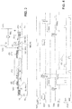
- the figure 5 represents a diagram of the potentials in the different regions of the pixel, for the different stages of a periodic cycle of integration, and considering two cases which are respectively a case of low illumination, therefore of low accumulation of charges in the photodiode, and a case of stronger illumination.
- the potential diagram is placed below the corresponding areas of the pixel, redrawn schematically on the figure 5 .
- the potential diagrams are defined with the increasing potentials downwards to allow a representation of the flows and storage of electric charges according to a hydraulic analogy, taking into account the fact that the charges are negative (electrons).
- phase 5A which is a “hard reset” phase of the storage node, we first apply to the first floating diffusion, from the drain 20 of the transistor T3, a first reset potential Vref1 lower than the potential Vpin2 of the PHa structure.
- This potential Vref1 will generally be greater than the internal potential Vpin1 of the photodiode, without this constituting a severe constraint, since in this “hard reset” phase 5A, the storage node is isolated from the photodiode (by the transistor T1).
- the control potential of the gate of transistor T3, equal for example to Vdd is greater than this reset potential Vref1. Any charges present in the storage node empty into drain 20; the potential of the structure PHa and the potential of the two floating diffusions take a value defined by the “hard reset” voltage (Vref1) applied at this moment to the drain of the reset transistor T3.
- phase 5B the second reset phase is carried out, in “soft reset” mode, with a potential Vref greater than Vref1 and for example equal to Vdd, on the drain of transistor T3.
- Vref a potential well in the first floating diffusion, the well whose bottom is at a high potential VH defined as a function of this reset voltage Vref.
- Vref is chosen so that the potential VH is greater than the intrinsic internal potential Vpin2 of the PHa structure which itself is greater than the intrinsic internal potential Vpin1 of the photodiode.
- the potential well does not extend to the second floating diffusion which does not touch the first and which does not receive the voltage Vref. It also does not extend under the self-biased diode PHa. But the internal potential of the second floating diffusion 184 aligns with the intrinsic internal potential of the diode PHa, that is to say Vpin2. The internal potential Vpin2 in the absence of charges from the second floating diffusion and from the self-polarized diode PHa then remains fixed throughout the duration of the read phase which follows this reset phase.
- phase 5C the potential barrier previously closed by the transfer gate G1 is lowered, to allow the transfer of charges from the photodiode to the storage node.
- the electrical charges accumulated in the photodiode flow into the potential well of the first floating diffusion.
- Curves 5D and 5D ′ show the potential diagrams after this discharge and after the end of the conduction of the transfer transistor T1, therefore after rising of the potential barrier which borders the photodiode.
- this is an assumption where the integrated charges are in small quantity, so that they do not overflow from the potential well created under the first diffusion.
- the charge-voltage conversion factor CVF is high; it only results from the (low) capacity of the first floating diffusion.
- the charges generated by the light were more numerous and they spontaneously overflow towards the two other parts of the storage node: PHa structure and second floating diffusion.
- the charges are then distributed among the different capacitors which are located in parallel: capacitance of the first floating diffusion, capacitance of the second floating diffusion, capacitance of the structure PHa, and auxiliary capacitance Cx.
- Any increase ⁇ Q in discharged charges results in a decrease in potential ⁇ Q / C where C is the sum of these four capacities.
- the conversion factor can be much lower, especially thanks to the auxiliary capacitor Cx which can be a capacitor to high density, that is to say high capacity per unit area if compared to the capacity per unit area of the first floating diffusion. It is therefore possible to measure both low illuminances with a high conversion factor and strong illuminances with a low conversion factor, and this automatically, that is to say without specific action to voluntarily modify the factor. conversion.
- the pixel comprises a transistor T5 for the global reinitialization of the photodiode.
- This transistor is however optional and it is possible to reset the photodiode through the transistor T1 and the transistor T3 made simultaneously conductive.
- a specific signal TRA ' (not shown) makes transistor T1 conductive while transistor T3 is turned on.
- the end of the signal TRA 'de fines the start of an integration period.
- the end of the TRA signal defines the end of the integration time.
- This sequencing in rolling shutter mode has the advantage of allowing a measurement by correlated double sampling which reduces the reading noise of the kTC type, but it has the drawback of making it more difficult to adjust the integration time and the drawback. to have a non-synchronous exposure of the different lines since it is necessary to provide an initial exposure offset from line to line.
- the fixing structure of the internal potential PHa may not consist of a self-polarized diode (N diffusion in the active layer P, surmounted by a surface diffusion P + at zero or fixed potential) but rather constituted of a simple gate isolated, placed above the active layer and brought to a chosen potential.
- the potential applied to this gate is chosen to fix the internal potential of the semiconductor between the two floating diffusions 182 and 184 at an intermediate value between the intrinsic internal potential Vpin1 of the photodiode and the potential VH of the bottom of the potential well of the first diffusion floating point 182.
- This intermediate value can be designated by Vpin2, by analogy with the value of the intrinsic internal potential of the self-polarized diode, since it plays the same role.
- the internal potential Vpin2 in the absence of charges from the second floating diffusion and from the region under this gate then remains fixed throughout the duration of the read phase which follows the reset phase.
- the quantity of charges which can be stored in low illumination mode is proportional to the difference VH-Vpin2 and to the value of the capacitance of the first floating diffusion.
- the quantity of additional charges that can be stored in high illumination mode is proportional to the difference Vpin2-Vpin1 but also proportional to the sum of the capacities of the storage node (three parts) and of the auxiliary capacity Cx.
- the second floating diffusion can have a very small surface area in the case where there is an auxiliary capacitor Cx, because its own capacitance then intervenes very little with respect to the value of the auxiliary capacitor Cx.
- the surface of the second floating diffusion can be limited to the surface necessary to make an electrical contact to the auxiliary capacitor.
- thermionic This risk concerns the case where a low illumination is measured in a pixel: the potential under the first floating diffusion after discharge of charges of the photodiode is greater than Vpin 2; but the potential in the adjacent structure PHa is Vpin2; electrons generated by the natural thermal activity of silicon in the PHa structure or in the second floating diffusion during the matrix read operation can be attracted to the potential well which is not filled up to Vpin2; these electrons, extracted from the second floating diffusion, tend to increase the potential of the latter, creating a potential pocket under the second floating diffusion.
- this pocket is filled, restoring the potential under the three parts of the storage node to the same value, this value being however less than Vpin2 because the reset potential in hard reset is lower. to Vpin2.
- the soft reset phase is carried out, with a higher potential Vref, which brings the potential back under the structure PHa and under the second floating diffusion to the value Vpin2 and which brings back the potential under the first floating diffusion to the value VH.
- the transfer gate G1 is composed of at least two successive gates between the photodiode and the first floating diffusion, with means for separately controlling the activation of these two gates.
- the aim is to further increase the charge storage capacity in the presence of strong illumination, while avoiding limiting to Vpin2-Vpin1 the maximum potential difference generated by the charges resulting from strong illumination.
- the figure 6 represents a pixel structure with a double transfer gate which makes it possible to go beyond this quantity.
- the double transfer gate comprises two adjacent gates which are the first gate G1a, adjacent to the photodiode, and the second gate G1b adjacent to the first floating diffusion 182.
- the other elements of the pixel are the same as those of the figure 3 .
- the floating diffusion 182, of the N + type extends under the whole of the second gate G1b (but not under the gate G1a or in all cases not under the gate portion G1a adjacent to the photodiode), so that charges coming from the photodiode and sufficiently numerous to overflow out of the potential well created under the floating diffusion 182, can now accumulate under the gate G1b .
- the absence of N + doping under the first transfer gate G1a maintains a potential step increasing the height of the potential barrier under gate G1a with respect to the barrier under gate G1b when the two gates receive the same potential.
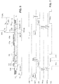
- the figure 7 represents the associated operating timing diagram, in which there is shown the signal TRAa controlling the conduction under the gate G1a and the signal TRAb controlling the conduction under the gate G1b.
- the conduction by the rising fronts of TRAa and TRAb is simultaneous, to allow the discharge of charges from the photodiode to the first floating diffusion 182.
- the interruption of conduction under the gate G1b by the falling front of TRAb is delayed compared to the interruption of conduction under the grid G1a by the falling edge of TRAa. There is therefore a moment when the potential under the gate G1b is high while it has returned to a low value under the gate G1a.
- This timing diagram is shown in the case of operation in “global shutter” mode in which the signals TRAa and TRAb are global for the entire matrix.
- the exposure time is adjusted globally by the signal GR controlling the gate G5.
- the other signals are the same as those explained with reference to the figure 4 : global reset signal Rstg then rolling reset signal Rstr; rolling line selection signals; read by an SHS sampling signal and an SHR sampling signal.
- the figure 8 represents the corresponding potential diagram, drawn in a case where there is a strong illumination, the case of the weak illumination being identical to that of the figure 5 without the falling edge shifted by the control of the gate G1b plays a significant role. More precisely, the figure 8A represents the accumulation of charges in the photodiode during the integration period and after the hard reset phase of the storage node according to the same principle as at the figure 5A . The figure 8B represents the distribution of potentials at the end of the soft reset phase (end of the global signal Rstg), according to the same principle as at the figure 5B .
- the figure 8C represents the transfer phase during which the two signals TRAa and TRAb are simultaneously brought to the high potential which allows the lowering of the potential barrier between the photodiode and the storage node.
- the charges of the photodiode are distributed in the three parts of the storage node, but also under the grid G1b. Beyond the charges which fill the potential well in the first floating diffusion, it is still possible to store a quantity of charges equal to the voltage difference Vpin2-Vpin1 multiplied by the sum of the capacities of the three parts of the storage node and of the capacity under the grid G1b. Beyond that, the charges would partly remain in the photodiode and would not be transferred to the storage node. We therefore now exceed the storage limit that appeared in the diagram of the figure 5D ' thanks to the G1b grid.
- the figure 8D represents the phase of closing of the gate G1a by the falling edge of the signal TRAa, while the gate G1b remains open due to the prolongation of the duration of the signal TRAb. Charges stored in the storage node cannot return to the photodiode.
- the figure 8E represents the last phase which is the closing of the barrier under the gate G1b by the falling edge of the signal TRAb.
- the charges which were under the grid G1b are pushed back towards the storage node. And it can be seen that these charges can make the potential of the storage node rise above the value Vpin1, which was not the case at the figure 5D ' .
- the transfer grid between the photodiode and the storage node comprises three successive juxtaposed partial grids. This variant allows, as we will see, to perform an integration in global shutter mode while allowing a differential reading by true double correlation in cases of low illumination.
- the figure 10 shows the corresponding chronogram, on which are indicated the global rising edges and falling edges for the whole matrix, as well as those which are "rolling" for a single row at a time.
- the signal TRAb the rising edge of which is global but the falling edge of which is “rolling”.
- the figure 11 represents the successive potential diagrams which result from this timing diagram.
- the charges generated by the light are stored in the photodiode and the global reset of the pixel has been performed by the global signal Rstg, preferably with the two steps of hard reset and soft reset.
- the potential barriers under the three gates are high (signals TRAa, TRAb, TRAc at low level).
- the potential step can be seen under the gate G1a, establishing on the side of the photodiode a potential barrier greater than the potential barrier under the gates G1b and G1c.
- a first sampling (SHR1) of the potential of the storage node is carried out, resulting from the charges present in the storage node; in the case of figure 11C , we can see that we simply sample a reset level of the storage node before discharge of charges. In the case of figure 11C ' , it can be seen that a level corresponding to the charges which overflowed towards the first floating diffusion 182 of the storage node is sampled and not a reset level.
- a second SHS sampling of the potential of the storage node is carried out for the line considered. This sampling represents the potential of the storage node resulting from the payloads.
- the storage node is reinitialized, in “rolling” mode, for the line considered and a third sampling (SHR2) of the potential of the storage node is carried out.
- the first and third samplings give different results, it is because there has been an overflow of charges at step 11C ′, the first sampling corresponding to the charges which have overflowed. In this case, it is because the illuminance is greater and a true correlated double sampling cannot be carried out.
- the illumination measurement is then determined by making the difference between the second SHS sampling (which corresponds to the sum of the transferred charges, including those which have overflowed) and the third SHR2 (which corresponds to a reset level after reading the payloads. then reset by the rolling signal Rstr).
- a comparison is therefore made between the first and third reading of the potential level of the first floating diffusion, to establish a measurement by difference between the second reading and the first reading or a measurement by difference between the second reading and the third reading according to the result of the comparison.
- the use of three transfer grids makes it possible to do a correlated double sampling for low light levels and this is what is desired since the correlated double sampling makes it possible to reduce the particularly annoying kTC noise at low light levels. illumination.
- This correlated double sampling is compatible with the operation in “global shutter” mode which has been described and with an adjustment of the integration time at will by the signal GR.
- the second floating diffusion is not adjacent to the reinitialization grid G3 and it is the first floating diffusion which is adjacent to this grid to allow the pixel reinitialization during each cycle. integration and reading. However, it is possible to provide an additional reset gate, not shown, adjacent to the second floating diffusion and making it possible to empty the charges of this second floating diffusion to a drain, not during normal operation but only for a calibration mode, for example the first time the sensor is used or each time the sensor is supplied with power. An integration and transfer cycle is carried out in the presence of light illuminating the entire matrix.
- the storage node is then reinitialized by the second floating diffusion without emptying the charges which fill up to the level Vpin2 the first floating diffusion, one reads the reset levels of all the pixels (line by line reading of the potential level of the first floating diffusion, for each pixel) and they are stored in a correction table which will subsequently be used to correct the level Vpin2 dispersions from pixel to pixel.
Landscapes
- Engineering & Computer Science (AREA)
- Multimedia (AREA)
- Signal Processing (AREA)
- Transforming Light Signals Into Electric Signals (AREA)
- Solid State Image Pick-Up Elements (AREA)
Claims (8)
- Bildsensor, der eine Matrix von aktiven Pixeln umfasst, wobei jedes Pixel eine Photodiode (PH) mit einem festen intrinsischen internen Potential, einen Speicherknoten (ND) zum Speichern von in der Photodiode integrierten Ladungen, mindestens ein Gate (G1) für den Transfer von Ladungen zwischen der Photodiode und dem Speicherknoten zum Steuern des Transfers von Ladungen von der Photodiode zum Speicherknoten nach einer Neuinitialisierungsphase des Speicherknotens, ein Gate (G3) zum Neuinitialisieren des Potentials des Speicherknotens und eine elektrische Verbindung zwischen dem Speicherknoten und dem Gate eines Lesetransistors (T2) umfasst, um eine Messung des Potentials des Speicherknotens während einer Lesephase nach der Neuinitialisierungsphase zu ermöglichen,
dadurch gekennzeichnet, dass der Speicherknoten drei Teile aufweist, die Folgendes umfassen:- eine erste schwebende Diffusion (182) neben dem Transfergate und dem Neuinitialisierungsgate, die über die elektrische Verbindung mit dem Gate des Lesetransistors verbunden ist,- eine zweite schwebende Diffusion (184) nicht neben der ersten schwebenden Diffusion, nicht neben dem Neuinitialisierungsgate und nicht mit dem Gate des Lesetransistors verbunden,- eine Struktur (PHa) zum Fixieren des internen Potentials, die die erste schwebende Diffusion von der zweiten schwebenden Diffusion trennt, wobei diese Struktur ein internes Potentialplateau in Abwesenheit von Ladungen zwischen den beiden schwebenden Diffusionen und in der zweiten schwebenden Diffusion auf einem festen Zwischenpotentialpegel (Vpin2) während der Lesephase einrichtet, das höher als das feste intrinsische interne Potential (Vpin1) der Photodiode, aber niedriger als ein Neuinitialisierungspotentialpegel (VH) der ersten schwebenden Diffusion ist, so dass die von der Photodiode in den Speicherknoten abgeführten Ladungen in der ersten schwebenden Diffusion eingeschlossen sind, aber, wenn sie zu zahlreich sind, spontan in die Struktur zum Fixieren des internen Potentials und in die zweite schwebende Diffusion überlaufen. - Bildsensor nach Anspruch 1, dadurch gekennzeichnet, dass eine Hilfskapazität (Cx), die Teil des Pixels bildet, durch eine elektrische Verbindung mit der zweiten schwebenden Diffusion verbunden ist.
- Bildsensor nach einem der Ansprüche 1 und 2, dadurch gekennzeichnet, dass das Ladungstransfergate aus einer Folge von mindestens zwei Transfergates (G1a, G1b) zwischen der Photodiode und dem Speicherknoten zusammengesetzt ist, wobei sich das erste Transfergate neben der Photodiode und das letzte Transfergate neben der ersten schwebenden Diffusion befindet, und dadurch, dass der Sensor Mittel zum separaten Anlegen von Steuerpotentialen an die verschiedenen Transfergates aufweist, um zunächst einen Ladungstransfer von der Photodiode zur ersten schwebenden Diffusion zu ermöglichen, dann eine Potentialbarriere zunächst unter dem ersten Transfergate und schließlich eine Potentialbarriere unter dem letzten Transfergate zu erhöhen.
- Bildsensor nach einem der Ansprüche 1 und 2, dadurch gekennzeichnet, dass das Transfergate aus einer Folge von drei Transfergates (Gla, G1b, G1c) zwischen der Photodiode und dem Speicherknoten zusammengesetzt ist, wobei sich das erste Transfergate (G1a) neben der Photodiode und das dritte Transfergate (G1c) neben der ersten schwebenden Diffusion befindet und das zweite Transfergate (G1b) sich zwischen dem ersten und dritten Transfergate befindet, und dadurch, dass der Sensor Mittel zum separaten Anlegen von Steuerpotentialen an die verschiedenen Transfergates aufweist, um zunächst über das erste Transfergate einen Ladungstransfer von der Photodiode zu einer unter dem zweiten Transfergate befindlichen Zone zu ermöglichen, dann eine Potentialbarriere unter dem ersten Transfergate einzurichten, dann nacheinander den Ladungstransfer von der unter dem zweiten Gate befindlichen Zone zur ersten schwebenden Diffusion zu ermöglichen und schließlich eine Potentialbarriere unter dem zweiten und dritten Transfergate zu erhöhen.
- Bildsensor nach Anspruch 4, dadurch gekennzeichnet, dass er Mittel aufweist, um der Reihe nach eine globale Neuinitialisierung der Potentiale des Speicherknotens durch Aktivieren des Neuinitialisierungsgates und eine globale Autorisierung eines Ladungstransfers von der Photodiode zu der unter dem zweiten Transfergate befindlichen Zone durch das erste und zweite Transfergate, gefolgt von einer globalen Hemmung dieses Transfers,
dann Zeile für Zeile Folgendes durchzuführen:- ein erstes Lesen des Potentialpegels der ersten schwebenden Diffusion,- einen Ladungstransfer von der unter dem zweiten Transfergate befindlichen Zone zur ersten schwebenden Diffusion und eventuell zur zweiten schwebenden Diffusion,- ein zweites Lesen des Potentialpegels der ersten schwebenden Diffusion,- ein Neuinitialisieren des Potentials der ersten schwebenden Diffusion,- ein drittes Lesen des Neuinitialisierungspotentialpegels der ersten schwebenden Diffusion,- und einen Vergleich zwischen dem ersten und dritten Ablesewert, um eine Messung anhand der Differenz zwischen dem zweiten Ablesewert und dem ersten Ablesewert oder eine Messung anhand der Differenz zwischen dem zweiten Ablesewert und dem dritten Ablesewert gemäß dem Ergebnis des Vergleichs zu erstellen. - Bildsensor nach einem der Ansprüche 1 bis 5, dadurch gekennzeichnet, dass die Struktur (PHa), die ein Potentialplateau mit einem festen internen Potentialpegel bildet, das die erste schwebende Diffusion von der zweiten schwebenden Diffusion trennt, eine Diode mit einem festen intrinsischen internen Potential ist, deren festes intrinsisches internes Potential höher ist als das feste intrinsische interne Potential der Photodiode.
- Bildsensor nach einem der Ansprüche 1 bis 5, dadurch gekennzeichnet, dass die Struktur (PHa), die ein Potentialplateau mit einem festen internen Potentialpegel bildet, das die erste schwebende Diffusion von der zweiten schwebenden Diffusion trennt, ein Gate ist, das ein festes Potential trägt, das eine Potentialbarriere mit einem Pegel bildet, der höher ist als das feste intrinsische interne Potential der Photodiode.
- Bildsensor nach einem der vorherigen Ansprüche, dadurch gekennzeichnet, dass er ein weiteres Neuinitialisierungsgate aufweist, dieses andere Gate sich neben der zweiten schwebenden Diffusion (184) befindet und zum Ermöglichen einer globalen Neuinitialisierung der Potentiale des Speicherknotens über die zweite schwebende Diffusion, ohne die in der ersten schwebenden Diffusion enthaltenen Ladungen zu entleeren, dann eines zeilenweisen Ablesens des Potentialpegels der ersten schwebenden Diffusion ausgelegt ist, die es ermöglicht, den Neuinitialisierungspegel jedes Pixels in einer Kalibrierungsphase zu erhalten und zu speichern.
Applications Claiming Priority (2)
| Application Number | Priority Date | Filing Date | Title |
|---|---|---|---|
| FR1555372A FR3037440B1 (fr) | 2015-06-12 | 2015-06-12 | Capteur d'image a haute dynamique, a nœud de stockage en trois parties |
| PCT/EP2016/062902 WO2016198402A1 (fr) | 2015-06-12 | 2016-06-07 | Capteur d'image a haute dynamique, a nœud de stockage en trois parties |
Publications (2)
| Publication Number | Publication Date |
|---|---|
| EP3308399A1 EP3308399A1 (de) | 2018-04-18 |
| EP3308399B1 true EP3308399B1 (de) | 2021-05-26 |
Family
ID=54356440
Family Applications (1)
| Application Number | Title | Priority Date | Filing Date |
|---|---|---|---|
| EP16731044.0A Active EP3308399B1 (de) | 2015-06-12 | 2016-06-07 | Bildsensor mit hohem dynamikbereich und dreiteiligem speicherknoten |
Country Status (4)
| Country | Link |
|---|---|
| EP (1) | EP3308399B1 (de) |
| FR (1) | FR3037440B1 (de) |
| TW (1) | TWI708923B (de) |
| WO (1) | WO2016198402A1 (de) |
Families Citing this family (5)
| Publication number | Priority date | Publication date | Assignee | Title |
|---|---|---|---|---|
| JP7455525B2 (ja) * | 2018-07-17 | 2024-03-26 | ブリルニクス シンガポール プライベート リミテッド | 固体撮像装置、固体撮像装置の製造方法、および電子機器 |
| TWI730868B (zh) * | 2020-08-06 | 2021-06-11 | 力晶積成電子製造股份有限公司 | 互補式金氧半導體影像感測器 |
| FR3124311B1 (fr) | 2021-06-16 | 2023-06-30 | St Microelectronics Crolles 2 Sas | Capteur photosensible et procédé de fabrication correspondant. |
| CN217983373U (zh) * | 2021-06-16 | 2022-12-06 | 意法半导体(克洛尔2)公司 | 光敏传感器 |
| CN115206940B (zh) * | 2022-06-30 | 2024-11-29 | 上海韦尔半导体股份有限公司 | 一种用于插指形光电二极管电势分析的测试结构与测试方法 |
Family Cites Families (8)
| Publication number | Priority date | Publication date | Assignee | Title |
|---|---|---|---|---|
| CN100525401C (zh) * | 2004-04-12 | 2009-08-05 | 国立大学法人东北大学 | 固体摄像装置、光传感器及固体摄像装置的动作方法 |
| JP4317115B2 (ja) * | 2004-04-12 | 2009-08-19 | 国立大学法人東北大学 | 固体撮像装置、光センサおよび固体撮像装置の動作方法 |
| US7821560B2 (en) * | 2005-04-07 | 2010-10-26 | Tohoku Universityu | Optical sensor, solid-state imaging device, and operating method of solid-state imaging device |
| KR100691183B1 (ko) * | 2005-06-21 | 2007-03-09 | 삼성전기주식회사 | 화소 단위의 포화 방지 기능을 구비한 이미지 센서 |
| US20070040922A1 (en) * | 2005-08-22 | 2007-02-22 | Micron Technology, Inc. | HDR/AB on multi-way shared pixels |
| KR101404074B1 (ko) * | 2007-07-31 | 2014-06-05 | 삼성전기주식회사 | Cmos 영상 센서 |
| FR2961631B1 (fr) * | 2010-06-18 | 2012-07-27 | E2V Semiconductors | Capteur d'image a pixel a six transistors |
| JP5664175B2 (ja) * | 2010-11-29 | 2015-02-04 | ソニー株式会社 | 固体撮像装置とその駆動方法、及び電子機器 |
-
2015
- 2015-06-12 FR FR1555372A patent/FR3037440B1/fr not_active Expired - Fee Related
-
2016
- 2016-06-07 EP EP16731044.0A patent/EP3308399B1/de active Active
- 2016-06-07 WO PCT/EP2016/062902 patent/WO2016198402A1/fr not_active Ceased
- 2016-06-08 TW TW105118263A patent/TWI708923B/zh not_active IP Right Cessation
Also Published As
| Publication number | Publication date |
|---|---|
| WO2016198402A1 (fr) | 2016-12-15 |
| TW201727193A (zh) | 2017-08-01 |
| FR3037440A1 (fr) | 2016-12-16 |
| EP3308399A1 (de) | 2018-04-18 |
| TWI708923B (zh) | 2020-11-01 |
| FR3037440B1 (fr) | 2019-11-08 |
Similar Documents
| Publication | Publication Date | Title |
|---|---|---|
| EP3332548B1 (de) | Verfahren zur steuerung eines aktiven pixelbildsensors | |
| EP2962330B1 (de) | Bildsensor mit überlaufschutzgate | |
| EP3188238B1 (de) | Flugzeit-erfassungspixel | |
| EP3117599B1 (de) | Verfahren zur bilderfassung mit verminderung von dunkelstrom und niedrigem verbrauch | |
| EP2216817B1 (de) | Von hinten beleuchteter halbleiter-bildsensor | |
| EP3308399B1 (de) | Bildsensor mit hohem dynamikbereich und dreiteiligem speicherknoten | |
| EP2752878B1 (de) | Bilderfassungssensor | |
| EP0435773B1 (de) | Bildaufnahmeeinrichtung mit integrierten Ablenkschaltungen | |
| EP2482317B1 (de) | Multilinearer Bildsensor mit Lastenintegration | |
| FR2953642A1 (fr) | Capteur d'image multilineaire a integration de charges. | |
| EP3406074A1 (de) | Verfahren zur steuerung eines aktiven pixelbildsensors | |
| EP1627432B1 (de) | Cmos bildaufnahmevorrichtung | |
| EP0276594A1 (de) | Überlaufvorrichtung für einen Ladungsübertragungs-Bildsensor und eine solche Vorrichtung enthaltender Bildsensor | |
| EP2845231B1 (de) | Matrixbildsensor für bidirektionale ladungsübertragung mit asymmetrischen gates | |
| FR2961631A1 (fr) | Capteur d'image a pixel a six transistors | |
| FR2513015A1 (fr) | Dispositif de detection d'image en couleurs du type transfert de charge | |
| WO2009068526A1 (fr) | Capteur d'image a pixel a quatre ou cinq transistors avec reduction de bruit de reinitialisation | |
| FR3011980A1 (fr) | Capteur d'image a multiplication d'electrons et a lecture regroupee de pixels | |
| WO2014060479A1 (fr) | Capteur d'image a efficacite quantique amelioree dans les grandes longueurs d'onde | |
| FR3109841A1 (fr) | Pixel comprenant une zone de stockage de charges | |
| FR2919961A1 (fr) | Capteur d'image a pixel cmos avec reduction de bruit de reinitialisation |
Legal Events
| Date | Code | Title | Description |
|---|---|---|---|
| STAA | Information on the status of an ep patent application or granted ep patent |
Free format text: STATUS: THE INTERNATIONAL PUBLICATION HAS BEEN MADE |
|
| PUAI | Public reference made under article 153(3) epc to a published international application that has entered the european phase |
Free format text: ORIGINAL CODE: 0009012 |
|
| STAA | Information on the status of an ep patent application or granted ep patent |
Free format text: STATUS: REQUEST FOR EXAMINATION WAS MADE |
|
| 17P | Request for examination filed |
Effective date: 20171129 |
|
| AK | Designated contracting states |
Kind code of ref document: A1 Designated state(s): AL AT BE BG CH CY CZ DE DK EE ES FI FR GB GR HR HU IE IS IT LI LT LU LV MC MK MT NL NO PL PT RO RS SE SI SK SM TR |
|
| AX | Request for extension of the european patent |
Extension state: BA ME |
|
| DAV | Request for validation of the european patent (deleted) | ||
| DAX | Request for extension of the european patent (deleted) | ||
| GRAP | Despatch of communication of intention to grant a patent |
Free format text: ORIGINAL CODE: EPIDOSNIGR1 |
|
| STAA | Information on the status of an ep patent application or granted ep patent |
Free format text: STATUS: GRANT OF PATENT IS INTENDED |
|
| INTG | Intention to grant announced |
Effective date: 20210201 |
|
| RIN1 | Information on inventor provided before grant (corrected) |
Inventor name: GESSET, STEPHANE Inventor name: FEREYRE, PIERRE Inventor name: MAYER, FREDERIC |
|
| GRAS | Grant fee paid |
Free format text: ORIGINAL CODE: EPIDOSNIGR3 |
|
| GRAA | (expected) grant |
Free format text: ORIGINAL CODE: 0009210 |
|
| STAA | Information on the status of an ep patent application or granted ep patent |
Free format text: STATUS: THE PATENT HAS BEEN GRANTED |
|
| AK | Designated contracting states |
Kind code of ref document: B1 Designated state(s): AL AT BE BG CH CY CZ DE DK EE ES FI FR GB GR HR HU IE IS IT LI LT LU LV MC MK MT NL NO PL PT RO RS SE SI SK SM TR |
|
| REG | Reference to a national code |
Ref country code: GB Ref legal event code: FG4D Free format text: NOT ENGLISH |
|
| REG | Reference to a national code |
Ref country code: CH Ref legal event code: EP |
|
| REG | Reference to a national code |
Ref country code: DE Ref legal event code: R096 Ref document number: 602016058389 Country of ref document: DE |
|
| REG | Reference to a national code |
Ref country code: AT Ref legal event code: REF Ref document number: 1397101 Country of ref document: AT Kind code of ref document: T Effective date: 20210615 |
|
| REG | Reference to a national code |
Ref country code: IE Ref legal event code: FG4D Free format text: LANGUAGE OF EP DOCUMENT: FRENCH |
|
| PGFP | Annual fee paid to national office [announced via postgrant information from national office to epo] |
Ref country code: FR Payment date: 20210625 Year of fee payment: 6 Ref country code: DE Payment date: 20210629 Year of fee payment: 6 Ref country code: NL Payment date: 20210626 Year of fee payment: 6 |
|
| REG | Reference to a national code |
Ref country code: NL Ref legal event code: FP |
|
| PGFP | Annual fee paid to national office [announced via postgrant information from national office to epo] |
Ref country code: GB Payment date: 20210628 Year of fee payment: 6 |
|
| REG | Reference to a national code |
Ref country code: LT Ref legal event code: MG9D |
|
| REG | Reference to a national code |
Ref country code: AT Ref legal event code: MK05 Ref document number: 1397101 Country of ref document: AT Kind code of ref document: T Effective date: 20210526 |
|
| PG25 | Lapsed in a contracting state [announced via postgrant information from national office to epo] |
Ref country code: FI Free format text: LAPSE BECAUSE OF FAILURE TO SUBMIT A TRANSLATION OF THE DESCRIPTION OR TO PAY THE FEE WITHIN THE PRESCRIBED TIME-LIMIT Effective date: 20210526 Ref country code: LT Free format text: LAPSE BECAUSE OF FAILURE TO SUBMIT A TRANSLATION OF THE DESCRIPTION OR TO PAY THE FEE WITHIN THE PRESCRIBED TIME-LIMIT Effective date: 20210526 Ref country code: HR Free format text: LAPSE BECAUSE OF FAILURE TO SUBMIT A TRANSLATION OF THE DESCRIPTION OR TO PAY THE FEE WITHIN THE PRESCRIBED TIME-LIMIT Effective date: 20210526 Ref country code: BG Free format text: LAPSE BECAUSE OF FAILURE TO SUBMIT A TRANSLATION OF THE DESCRIPTION OR TO PAY THE FEE WITHIN THE PRESCRIBED TIME-LIMIT Effective date: 20210826 Ref country code: AT Free format text: LAPSE BECAUSE OF FAILURE TO SUBMIT A TRANSLATION OF THE DESCRIPTION OR TO PAY THE FEE WITHIN THE PRESCRIBED TIME-LIMIT Effective date: 20210526 |
|
| PG25 | Lapsed in a contracting state [announced via postgrant information from national office to epo] |
Ref country code: PT Free format text: LAPSE BECAUSE OF FAILURE TO SUBMIT A TRANSLATION OF THE DESCRIPTION OR TO PAY THE FEE WITHIN THE PRESCRIBED TIME-LIMIT Effective date: 20210927 Ref country code: PL Free format text: LAPSE BECAUSE OF FAILURE TO SUBMIT A TRANSLATION OF THE DESCRIPTION OR TO PAY THE FEE WITHIN THE PRESCRIBED TIME-LIMIT Effective date: 20210526 Ref country code: NO Free format text: LAPSE BECAUSE OF FAILURE TO SUBMIT A TRANSLATION OF THE DESCRIPTION OR TO PAY THE FEE WITHIN THE PRESCRIBED TIME-LIMIT Effective date: 20210826 Ref country code: RS Free format text: LAPSE BECAUSE OF FAILURE TO SUBMIT A TRANSLATION OF THE DESCRIPTION OR TO PAY THE FEE WITHIN THE PRESCRIBED TIME-LIMIT Effective date: 20210526 Ref country code: SE Free format text: LAPSE BECAUSE OF FAILURE TO SUBMIT A TRANSLATION OF THE DESCRIPTION OR TO PAY THE FEE WITHIN THE PRESCRIBED TIME-LIMIT Effective date: 20210526 Ref country code: LV Free format text: LAPSE BECAUSE OF FAILURE TO SUBMIT A TRANSLATION OF THE DESCRIPTION OR TO PAY THE FEE WITHIN THE PRESCRIBED TIME-LIMIT Effective date: 20210526 Ref country code: IS Free format text: LAPSE BECAUSE OF FAILURE TO SUBMIT A TRANSLATION OF THE DESCRIPTION OR TO PAY THE FEE WITHIN THE PRESCRIBED TIME-LIMIT Effective date: 20210926 Ref country code: GR Free format text: LAPSE BECAUSE OF FAILURE TO SUBMIT A TRANSLATION OF THE DESCRIPTION OR TO PAY THE FEE WITHIN THE PRESCRIBED TIME-LIMIT Effective date: 20210827 |
|
| PG25 | Lapsed in a contracting state [announced via postgrant information from national office to epo] |
Ref country code: ES Free format text: LAPSE BECAUSE OF FAILURE TO SUBMIT A TRANSLATION OF THE DESCRIPTION OR TO PAY THE FEE WITHIN THE PRESCRIBED TIME-LIMIT Effective date: 20210526 Ref country code: RO Free format text: LAPSE BECAUSE OF FAILURE TO SUBMIT A TRANSLATION OF THE DESCRIPTION OR TO PAY THE FEE WITHIN THE PRESCRIBED TIME-LIMIT Effective date: 20210526 Ref country code: CZ Free format text: LAPSE BECAUSE OF FAILURE TO SUBMIT A TRANSLATION OF THE DESCRIPTION OR TO PAY THE FEE WITHIN THE PRESCRIBED TIME-LIMIT Effective date: 20210526 Ref country code: EE Free format text: LAPSE BECAUSE OF FAILURE TO SUBMIT A TRANSLATION OF THE DESCRIPTION OR TO PAY THE FEE WITHIN THE PRESCRIBED TIME-LIMIT Effective date: 20210526 Ref country code: DK Free format text: LAPSE BECAUSE OF FAILURE TO SUBMIT A TRANSLATION OF THE DESCRIPTION OR TO PAY THE FEE WITHIN THE PRESCRIBED TIME-LIMIT Effective date: 20210526 Ref country code: SM Free format text: LAPSE BECAUSE OF FAILURE TO SUBMIT A TRANSLATION OF THE DESCRIPTION OR TO PAY THE FEE WITHIN THE PRESCRIBED TIME-LIMIT Effective date: 20210526 Ref country code: SK Free format text: LAPSE BECAUSE OF FAILURE TO SUBMIT A TRANSLATION OF THE DESCRIPTION OR TO PAY THE FEE WITHIN THE PRESCRIBED TIME-LIMIT Effective date: 20210526 |
|
| REG | Reference to a national code |
Ref country code: CH Ref legal event code: PL |
|
| REG | Reference to a national code |
Ref country code: DE Ref legal event code: R097 Ref document number: 602016058389 Country of ref document: DE |
|
| REG | Reference to a national code |
Ref country code: BE Ref legal event code: MM Effective date: 20210630 |
|
| PLBE | No opposition filed within time limit |
Free format text: ORIGINAL CODE: 0009261 |
|
| STAA | Information on the status of an ep patent application or granted ep patent |
Free format text: STATUS: NO OPPOSITION FILED WITHIN TIME LIMIT |
|
| PG25 | Lapsed in a contracting state [announced via postgrant information from national office to epo] |
Ref country code: MC Free format text: LAPSE BECAUSE OF FAILURE TO SUBMIT A TRANSLATION OF THE DESCRIPTION OR TO PAY THE FEE WITHIN THE PRESCRIBED TIME-LIMIT Effective date: 20210526 Ref country code: LU Free format text: LAPSE BECAUSE OF NON-PAYMENT OF DUE FEES Effective date: 20210607 |
|
| PG25 | Lapsed in a contracting state [announced via postgrant information from national office to epo] |
Ref country code: LI Free format text: LAPSE BECAUSE OF NON-PAYMENT OF DUE FEES Effective date: 20210630 Ref country code: IE Free format text: LAPSE BECAUSE OF NON-PAYMENT OF DUE FEES Effective date: 20210607 Ref country code: CH Free format text: LAPSE BECAUSE OF NON-PAYMENT OF DUE FEES Effective date: 20210630 |
|
| 26N | No opposition filed |
Effective date: 20220301 |
|
| PG25 | Lapsed in a contracting state [announced via postgrant information from national office to epo] |
Ref country code: IS Free format text: LAPSE BECAUSE OF FAILURE TO SUBMIT A TRANSLATION OF THE DESCRIPTION OR TO PAY THE FEE WITHIN THE PRESCRIBED TIME-LIMIT Effective date: 20210926 Ref country code: AL Free format text: LAPSE BECAUSE OF FAILURE TO SUBMIT A TRANSLATION OF THE DESCRIPTION OR TO PAY THE FEE WITHIN THE PRESCRIBED TIME-LIMIT Effective date: 20210526 |
|
| PG25 | Lapsed in a contracting state [announced via postgrant information from national office to epo] |
Ref country code: IT Free format text: LAPSE BECAUSE OF FAILURE TO SUBMIT A TRANSLATION OF THE DESCRIPTION OR TO PAY THE FEE WITHIN THE PRESCRIBED TIME-LIMIT Effective date: 20210526 Ref country code: BE Free format text: LAPSE BECAUSE OF NON-PAYMENT OF DUE FEES Effective date: 20210630 |
|
| REG | Reference to a national code |
Ref country code: DE Ref legal event code: R119 Ref document number: 602016058389 Country of ref document: DE |
|
| REG | Reference to a national code |
Ref country code: NL Ref legal event code: MM Effective date: 20220701 |
|
| GBPC | Gb: european patent ceased through non-payment of renewal fee |
Effective date: 20220607 |
|
| PG25 | Lapsed in a contracting state [announced via postgrant information from national office to epo] |
Ref country code: NL Free format text: LAPSE BECAUSE OF NON-PAYMENT OF DUE FEES Effective date: 20220701 |
|
| PG25 | Lapsed in a contracting state [announced via postgrant information from national office to epo] |
Ref country code: FR Free format text: LAPSE BECAUSE OF NON-PAYMENT OF DUE FEES Effective date: 20220630 |
|
| PG25 | Lapsed in a contracting state [announced via postgrant information from national office to epo] |
Ref country code: GB Free format text: LAPSE BECAUSE OF NON-PAYMENT OF DUE FEES Effective date: 20220607 Ref country code: DE Free format text: LAPSE BECAUSE OF NON-PAYMENT OF DUE FEES Effective date: 20230103 |
|
| PG25 | Lapsed in a contracting state [announced via postgrant information from national office to epo] |
Ref country code: CY Free format text: LAPSE BECAUSE OF FAILURE TO SUBMIT A TRANSLATION OF THE DESCRIPTION OR TO PAY THE FEE WITHIN THE PRESCRIBED TIME-LIMIT Effective date: 20210526 |
|
| PG25 | Lapsed in a contracting state [announced via postgrant information from national office to epo] |
Ref country code: HU Free format text: LAPSE BECAUSE OF FAILURE TO SUBMIT A TRANSLATION OF THE DESCRIPTION OR TO PAY THE FEE WITHIN THE PRESCRIBED TIME-LIMIT; INVALID AB INITIO Effective date: 20160607 |
|
| PG25 | Lapsed in a contracting state [announced via postgrant information from national office to epo] |
Ref country code: MK Free format text: LAPSE BECAUSE OF FAILURE TO SUBMIT A TRANSLATION OF THE DESCRIPTION OR TO PAY THE FEE WITHIN THE PRESCRIBED TIME-LIMIT Effective date: 20210526 |
|
| PG25 | Lapsed in a contracting state [announced via postgrant information from national office to epo] |
Ref country code: TR Free format text: LAPSE BECAUSE OF FAILURE TO SUBMIT A TRANSLATION OF THE DESCRIPTION OR TO PAY THE FEE WITHIN THE PRESCRIBED TIME-LIMIT Effective date: 20210526 |
|
| PG25 | Lapsed in a contracting state [announced via postgrant information from national office to epo] |
Ref country code: MT Free format text: LAPSE BECAUSE OF FAILURE TO SUBMIT A TRANSLATION OF THE DESCRIPTION OR TO PAY THE FEE WITHIN THE PRESCRIBED TIME-LIMIT Effective date: 20210526 |