EP3309647A1 - Steuerungsvorrichtung und kommunikationsvorrichtung - Google Patents
Steuerungsvorrichtung und kommunikationsvorrichtung Download PDFInfo
- Publication number
- EP3309647A1 EP3309647A1 EP17191562.2A EP17191562A EP3309647A1 EP 3309647 A1 EP3309647 A1 EP 3309647A1 EP 17191562 A EP17191562 A EP 17191562A EP 3309647 A1 EP3309647 A1 EP 3309647A1
- Authority
- EP
- European Patent Office
- Prior art keywords
- timer
- time
- communication
- synchronization
- external device
- Prior art date
- Legal status (The legal status is an assumption and is not a legal conclusion. Google has not performed a legal analysis and makes no representation as to the accuracy of the status listed.)
- Granted
Links
Images






Classifications
-
- H—ELECTRICITY
- H04—ELECTRIC COMMUNICATION TECHNIQUE
- H04L—TRANSMISSION OF DIGITAL INFORMATION, e.g. TELEGRAPHIC COMMUNICATION
- H04L69/00—Network arrangements, protocols or services independent of the application payload and not provided for in the other groups of this subclass
- H04L69/28—Timers or timing mechanisms used in protocols
-
- G—PHYSICS
- G06—COMPUTING OR CALCULATING; COUNTING
- G06F—ELECTRIC DIGITAL DATA PROCESSING
- G06F1/00—Details not covered by groups G06F3/00 - G06F13/00 and G06F21/00
- G06F1/04—Generating or distributing clock signals or signals derived directly therefrom
- G06F1/12—Synchronisation of different clock signals provided by a plurality of clock generators
-
- H—ELECTRICITY
- H04—ELECTRIC COMMUNICATION TECHNIQUE
- H04L—TRANSMISSION OF DIGITAL INFORMATION, e.g. TELEGRAPHIC COMMUNICATION
- H04L7/00—Arrangements for synchronising receiver with transmitter
- H04L7/0016—Arrangements for synchronising receiver with transmitter correction of synchronization errors
-
- G—PHYSICS
- G05—CONTROLLING; REGULATING
- G05B—CONTROL OR REGULATING SYSTEMS IN GENERAL; FUNCTIONAL ELEMENTS OF SUCH SYSTEMS; MONITORING OR TESTING ARRANGEMENTS FOR SUCH SYSTEMS OR ELEMENTS
- G05B19/00—Program-control systems
- G05B19/02—Program-control systems electric
- G05B19/418—Total factory control, i.e. centrally controlling a plurality of machines, e.g. direct or distributed numerical control [DNC], flexible manufacturing systems [FMS], integrated manufacturing systems [IMS] or computer integrated manufacturing [CIM]
- G05B19/4185—Total factory control, i.e. centrally controlling a plurality of machines, e.g. direct or distributed numerical control [DNC], flexible manufacturing systems [FMS], integrated manufacturing systems [IMS] or computer integrated manufacturing [CIM] characterised by the network communication
-
- G—PHYSICS
- G06—COMPUTING OR CALCULATING; COUNTING
- G06F—ELECTRIC DIGITAL DATA PROCESSING
- G06F1/00—Details not covered by groups G06F3/00 - G06F13/00 and G06F21/00
- G06F1/04—Generating or distributing clock signals or signals derived directly therefrom
- G06F1/14—Time supervision arrangements, e.g. real time clock
-
- H—ELECTRICITY
- H04—ELECTRIC COMMUNICATION TECHNIQUE
- H04L—TRANSMISSION OF DIGITAL INFORMATION, e.g. TELEGRAPHIC COMMUNICATION
- H04L12/00—Data switching networks
- H04L12/28—Data switching networks characterised by path configuration, e.g. LAN [Local Area Networks] or WAN [Wide Area Networks]
- H04L12/40—Bus networks
-
- H—ELECTRICITY
- H04—ELECTRIC COMMUNICATION TECHNIQUE
- H04L—TRANSMISSION OF DIGITAL INFORMATION, e.g. TELEGRAPHIC COMMUNICATION
- H04L12/00—Data switching networks
- H04L12/28—Data switching networks characterised by path configuration, e.g. LAN [Local Area Networks] or WAN [Wide Area Networks]
- H04L12/40—Bus networks
- H04L12/40169—Flexible bus arrangements
- H04L12/40176—Flexible bus arrangements involving redundancy
-
- H—ELECTRICITY
- H04—ELECTRIC COMMUNICATION TECHNIQUE
- H04L—TRANSMISSION OF DIGITAL INFORMATION, e.g. TELEGRAPHIC COMMUNICATION
- H04L12/00—Data switching networks
- H04L12/28—Data switching networks characterised by path configuration, e.g. LAN [Local Area Networks] or WAN [Wide Area Networks]
- H04L12/40—Bus networks
- H04L12/407—Bus networks with decentralised control
-
- H—ELECTRICITY
- H04—ELECTRIC COMMUNICATION TECHNIQUE
- H04L—TRANSMISSION OF DIGITAL INFORMATION, e.g. TELEGRAPHIC COMMUNICATION
- H04L7/00—Arrangements for synchronising receiver with transmitter
- H04L7/0008—Synchronisation information channels, e.g. clock distribution lines
-
- G—PHYSICS
- G05—CONTROLLING; REGULATING
- G05B—CONTROL OR REGULATING SYSTEMS IN GENERAL; FUNCTIONAL ELEMENTS OF SUCH SYSTEMS; MONITORING OR TESTING ARRANGEMENTS FOR SUCH SYSTEMS OR ELEMENTS
- G05B2219/00—Program-control systems
- G05B2219/30—Nc systems
- G05B2219/31—From computer integrated manufacturing till monitoring
- G05B2219/31213—Synchronization of servers in network
-
- H—ELECTRICITY
- H04—ELECTRIC COMMUNICATION TECHNIQUE
- H04L—TRANSMISSION OF DIGITAL INFORMATION, e.g. TELEGRAPHIC COMMUNICATION
- H04L12/00—Data switching networks
- H04L12/28—Data switching networks characterised by path configuration, e.g. LAN [Local Area Networks] or WAN [Wide Area Networks]
- H04L12/40—Bus networks
- H04L2012/40208—Bus networks characterized by the use of a particular bus standard
- H04L2012/40215—Controller Area Network CAN
-
- H—ELECTRICITY
- H04—ELECTRIC COMMUNICATION TECHNIQUE
- H04L—TRANSMISSION OF DIGITAL INFORMATION, e.g. TELEGRAPHIC COMMUNICATION
- H04L12/00—Data switching networks
- H04L12/28—Data switching networks characterised by path configuration, e.g. LAN [Local Area Networks] or WAN [Wide Area Networks]
- H04L12/40—Bus networks
- H04L2012/40208—Bus networks characterized by the use of a particular bus standard
- H04L2012/40221—Profibus
-
- H—ELECTRICITY
- H04—ELECTRIC COMMUNICATION TECHNIQUE
- H04L—TRANSMISSION OF DIGITAL INFORMATION, e.g. TELEGRAPHIC COMMUNICATION
- H04L12/00—Data switching networks
- H04L12/28—Data switching networks characterised by path configuration, e.g. LAN [Local Area Networks] or WAN [Wide Area Networks]
- H04L12/40—Bus networks
- H04L2012/4026—Bus for use in automation systems
Definitions
- the present invention relates to a control device and a communication device that constitute a control system for controlling machines or facilities.
- a control device such as a programmable logic controller (PLC) has spread as a main component for realizing various types of factory automation (FA).
- PLC programmable logic controller
- FA factory automation
- a delay based on transmission of data occurs.
- the magnitude of such a transmission delay varies depending on positions to which the functional units are connected. There is a likelihood that times at which the functional units acquire input data and output data will vary depending on the variation of the delay time.
- Patent Document 1 discloses an environment in which a synchronization time in a control system including a master device and one or more slave devices connected thereto via a network can be easily determined.
- the control system disclosed in Patent Document 1 performs time synchronization between associated devices or units and performs necessary processes at designated times.
- Patent Document 1 Japanese Unexamined Patent Application Publication No. 2014-120884
- Patent Document 1 does not disclose time synchronization between different protocols.
- An object of the present invention is to provide a new configuration for realizing time synchronization between different protocols.
- a control device constituting a control system for controlling machines or facilities.
- the control device includes first communication means configured to transmit and receive data in accordance with a first protocol.
- the first communication means includes a first timer that defines a time of data transmission and is time-synchronized with an entity to and from which data is transmitted and received.
- the control device includes second communication means configured to transmit and receive data in accordance with a second protocol different from the first protocol.
- the second communication means includes a second timer that defines a time of data transmission and is time-synchronized with an entity to and from which data is transmitted and received.
- the control device includes synchronization means configured to time-synchronize the first timer and the second timer.
- the synchronization means time-corrects the second timer with respect to the first timer.
- the synchronization means time-synchronizes each entity time-synchronized with the second communication means with the second timer which has been time-corrected.
- the synchronization means includes: means configured to set the first timer to output a synchronization signal to the second timer every predetermined cycle; means configured to notify the second timer of a first time in the first timer indicating a time at which the synchronization signal is output and which is set in the first timer; and means configured to time-correct the second timer on the basis of a difference between the first time and a second time in the second timer at which the synchronization signal output from the first timer is detected by the second timer.
- control device further includes an interface for connection to an external device including a third timer.
- the synchronization means time-corrects the first timer and the second timer with respect to the third timer of the external device.
- the external device is connected to the control device via communication means which is independent from the first communication means and the second communication means.
- the external device is connected to the control device via an entity that transmits and receives data to and from any one of the first communication means and the second communication means.
- the synchronization means includes: means configured to set the third timer to output a synchronization signal to the first timer at a designated third time; means configured to read a fourth time in the first timer which is stored when the synchronization signal output from the third timer is detected by the first timer from the first timer; and means configured to instruct the first timer to correct time on the basis of a difference between the third time and the fourth time.
- the synchronization means includes means configured to provide setting for a noise filter included in the first timer.
- the first timer compensates for a time delay generated due to the noise filter on the basis of the setting for the noise filter and then stores the fourth time.
- a communication device includes first communication means configured to transmit and receive data in accordance with a first protocol.
- the first communication means includes a first timer that defines a time of data transmission and is time-synchronized with an entity to and from which data is transmitted and received.
- the communication device includes second communication means configured to transmit and receive data in accordance with a second protocol different from the first protocol.
- the second communication means includes a second timer that defines a time of data transmission and is time-synchronized with an entity to and from which data is transmitted and received.
- the communication device includes synchronization means configured to time-synchronize the first timer and the second timer.
- control system based on a programmable logic controller (PLC) will be described as a specific example, but the technical spirit disclosed in this specification can be applied to an arbitrary control device without being limited to the name PLC.
- PLC programmable logic controller
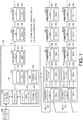
- FIG. 1 is a schematic diagram illustrating a configuration of principal parts of the control system 1 according to this embodiment.
- the control system 1 mainly controls machines or facilities.
- the control system 1 includes one or more communication means and data is transmitted and received via the communication means.
- “communication means” includes an entire framework for transmitting and receiving data between a plurality of entities (for example, devices or units) in accordance with a certain protocol.
- “communication means” may be one of a parallel communication mode and a serial communication mode or may be one of a bus and a network.
- control system 1 includes a CPU unit 100 that constitutes the PLC and one or more communication coupler units 200-1, 200-2, ... (hereinafter generically referred to as "communication coupler units 200") that are connected thereto via a field network 3.
- the CPU unit 100 or each communication coupler unit 200 may be equipped with one or more functional units.
- a set of a communication coupler unit 200 and one or more functional units may be referred to as a remote I/O device.
- the local bus 2, the field network 3, the local bus 4-1, and the local bus 4-2 employ communication modes which are suitable for transmitting and receiving field data.
- a communication mode in which a transmission time of data is guaranteed may be employed as an example of such communication modes.
- a type of fixed-cycle bus or a type of fixed-cycle network is employed by such communication modes.
- An arbitrary bus communication mode can be employed as the fixed-cycle bus.
- a network associated with known protocols such as EtherCAT (registered trademark), EtherNet/IP (registered trademark), DeviceNet (registered trademark), and CompoNet (registered trademark) may be employed as the fixed-cycle network.
- the same function as the fixed-cycle bus or the fixed-cycle network can be realized by scheduling a data transmission time in consideration of a margin corresponding to fluctuation of a transmission time.
- a configuration in which units associated with data transmission include timers which are time-synchronized with each other is supposed. That is, in each bus or each network, the units transmit or receive data at a time which is designated using timers time-synchronized with each other.
- the local bus 2, the field network 3, and the local buses 4 may employ the same protocol or may employ protocols independent from each other. Regardless of what protocol is employed, it is assumed that a timer serving as a reference for data transmission is provided.
- a real-time clock may be employed as a timer, but a free-run counter (hereinafter also referred to as "FRC") that counts up (increments) at a predetermined cycle is used in this embodiment.
- FRC free-run counter
- a current time can be calculated using a counter value output from the free-run counter as an elapsed time from a certain time point, and thus the free-run counter can function as a timer.
- the local bus 2, the field network 3, and the local buses 4 are named for the purpose of convenience of explanation, and the technical scope of the present invention is not limited by the names.
- the CPU unit 100 is an element constituting the control system 1 including the PLC and corresponds to a control device that controls processing in the control system 1.
- the CPU unit 100 and one or more functional units 150 are connected to each other via the local bus 2 which is an example of communication means. Accordingly, the CPU unit 100 also functions as a type of communication device.
- the CPU unit 100 includes a processor 102, a memory 104, a communication control circuit 110, a network interface card (hereinafter also abbreviated to "NIC") 120, a bus master circuit 130, and an external interface 140.
- NIC network interface card
- the processor 102 executes a program stored in the memory 104 or the like. For the purpose of convenience of explanation, only one processor 102 is illustrated in FIG. 1 , but a plurality of processors may be mounted. Each processor may include a plurality of cores.
- the memory 104 includes a portion (typically, a volatile memory) that provides a work area required for execution of a program in the processor 102 and a portion (typically, a nonvolatile memory) that stores the program which is executed by the processor 102.
- a dynamic random access memory (DRAM), a static random access memory (SRAM), or the like can be used as the volatile memory and a flash memory, a hard disk, or the like can be used as the nonvolatile memory.
- DRAM dynamic random access memory
- SRAM static random access memory
- the memory 104 stores a user program 106, a system program 108, and the like.
- the system program 108 includes an operating system (OS) for allowing the processor 102 to execute the user program 106 and a library.
- the user program 106 typically includes commands for performing a process of acquiring data (input data) collected by one or more functional units or a process of generating data (output data) to be transmitted to one or more functional units, and is arbitrarily prepared depending on machines or facilities that are control targets.
- the communication control circuit 110 has a function of relaying a request between the processor 102, the NIC 120, and the bus master circuit 130 and, for example, requests the NIC 120 and/or the bus master circuit 130 to transmit output data in response to a communication request from the processor 102.
- the communication control circuit 110 includes a control logic 112 and a timer 114.
- the control logic 112 is a portion that accomplishes a duty imposed on the communication control circuit 110 and is embodied by software and/or by hardware.
- the timer 114 includes a free-run counter that generates a pulse (a clock) serving as a reference for a control time in the control logic 112.
- the communication control circuit 110 has a hard-wired configuration and realize faster processing than the processor 102. That is, the communication control circuit 110 is embodied using a hardware logic.
- the communication control circuit 110 may be embodied using a field-programmable gate array (FPGA) which is an example of a programmable logic device (PLD), an application specific integrated circuit (ASIC) which is an example of an integrated circuit (IC), or the like.
- FPGA field-programmable gate array
- PLA programmable logic device
- ASIC application specific integrated circuit
- IC integrated circuit
- a system-on-chip (SOC) 101 in which the processor 102, the communication control circuit 110, and the NIC 120 are mounted on the same chip is configured.
- SOC system-on-chip
- the present invention is not limited to such a configuration, and the units may be mounted on different chips or the entire units may be mounted together on the same chip.
- Such mounting types can be appropriately selected in consideration of required performance, costs, or the like.
- the NIC 120 functions as a communication master that manages data transmission over the field network 3. That is, the NIC 120 transmits and receives data to and from a remote I/O device (the communication coupler units 200 and the functional units mounted in the communication coupler units 200) via the field network 3 which is an example of communication means.
- the NIC 120 includes a control logic 122 that manages data transmission over the field network 3. More specifically, the control logic 122 performs time management and transmission/reception time management for guaranteeing a transmission time of data which is transmitted over the field network 3. As will be described later, the control logic 122 of the NIC 120 determines a control time on the basis of a time which is managed by the timer 114 of the communication control circuit 110.
- the bus master circuit 130 functions as a communication master that manages data transmission over the local bus 2. That is, the bus master circuit 130 transmits and receives data to and from the functional units 150 which are mounted in the CPU unit 100 via the local bus 2 which is an example of communication means.
- the bus master circuit 130 includes a control logic 132 that manages data transmission over the local bus 2 and a timer 134 that determines a control time in the control logic 132.
- the control logic 132 performs time management and transmission/reception time management for guaranteeing a transmission time of data which is transmitted over the local bus 2.
- the external interface 140 relays transmission and reception of data to and from an arbitrary external device 300.
- An interface using a versatile interface standard such as PC Express or Universal Serial Bus (USB) can be employed as the external interface 140. That is, the external device 300 may be connected to the CPU unit 100 via communication means independent from the local bus 2 or the field network 3.
- an external device including a timer serving as a reference for time synchronization can be employed as the external device 300. A configuration using the timer included in the external device 300 will be described later.
- the functional units 150 provide various functions required for the control system 1 to realize control of various machines or facilities. Typically, each functional unit 150 performs collection of field information in machines or facilities that are control targets, output of a command signal to the machines or facilities that are control targets, and the like.
- Each functional unit 150 functions as a bus slave that performs data transmission under the control of the bus master circuit 130 of the CPU unit 100. More specifically, regarding data transmission over the local bus 2, each functional unit 150 includes a control logic 152 that manages data transmission over the local bus 2 and a timer 154 that determines a control time in the control logic 152.
- the control logic 152 manages a time at which data transmitted over the local bus 2 is transmitted or received in accordance with a command from the bus master circuit 130.
- the control logic 152 monitors and adjusts a time at which the timer 154 generates a pulse in time-synchronization with the timer 134 of the bus master circuit 130.
- the communication coupler unit 200 functions as a relay device that relays transmission and reception of data between one or more functional units 150 attached to the communication coupler units 200 via the local buses 4 and the CPU unit 100. More specifically, the communication coupler unit 200 includes a network interface circuit 210 and a bus master circuit 220.
- the network interface circuit 210 functions as a network slave that performs data transmission over the field network 3 under the control of the NIC 120 of the CPU unit 100. More specifically, the network interface circuit 210 includes a control logic 212 that manages data transmission over the field network 3 and a timer 214 that determines a control time in the control logic 212. The control logic 212 manages a time at which data transmitted over the field network 3 is transmitted or received in accordance with a command from the NIC 120. The control logic 212 monitors and adjusts a time at which the timer 214 generates a pulse in time-synchronization with the timer of the NIC 120.
- the bus master circuit 220 has the same function as the bus master circuit 130 of the CPU unit 100 and functions as a communication master that manages data transmission over the local buses 4. That is, the bus master circuit 220 transmits and receives data to and from the functional units 150 attached to the communication coupler units 200 via the local buses 4 which are an example of communication means.
- the bus master circuit 220 includes a control logic 222 that manages data transmission over the local buses 4 and a timer 224 that determines a control time in the control logic 222.
- the control logic 222 performs time management and transmission/reception time management for guaranteeing a transmission time of data which is transmitted over the local buses 4.
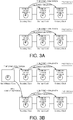
- FIGs. 2A, 2B , 3A and 3B are schematic diagrams illustrating a time synchronization function which is provided by the control system 1 according to this embodiment.
- FIG. 2A illustrates a configuration in which data communication is performed in accordance with two different protocols (protocol 1 and protocol 2). Specifically, communication master A and a plurality of communication slaves A1, A2, ... are connected to each other in a configuration example according to protocol 1, and communication master B and a plurality of communication slaves B1, B2, ... are connected to each other in a configuration example according to protocol 2.
- Each of communication master A and communication master B includes a timer functioning as a boundary clock and time-synchronizes timers of the communication slaves connected thereto via a bus/network in accordance with a synchronization procedure of each protocol.
- Each of the plurality of communication slaves A1, A2, ... and each of the plurality of communication slaves B1, B2, ... include a timer functioning as an ordinary clock.
- communication master A corresponds to communication means that transmits and receives data to and from the plurality of communication slaves A1, A2, ... in accordance with protocol 1.
- Communication master A which is the communication means includes a timer that defines a time of data transmission and that is time-synchronized with entities (that is, communication slaves A1, A2, ...) to and from which data is transmitted and received.
- communication master B corresponds to communication means that transmits and receives data to and from the plurality of communication slaves B1, B2, ... in accordance with protocol 2 which is different from protocol 1.
- Communication master B which is the communication means includes a timer that defines a time of data transmission and that is time-synchronized with entities (that is, communication slaves B1, B2, ...) to and from which data is transmitted and received.
- a timer of one of communication master A and communication master B functions as a master of the whole control system 1.
- the master of the whole system is also referred to as a "grand master clock.”
- FIGs. 2A and 2B only two communication masters are illustrated, but three or more communication masters may be present. In this case, a timer of any one communication master can be set as the grand master clock.
- the timer of communication master A is set as the grand master clock
- communication master B is time-synchronized with the grand master clock.
- the configuration according to protocol 1 and the configuration according to protocol 2 can be time-synchronized with each other. That is, the control system 1 according to this embodiment has a synchronization function of time-synchronizing the timer time-synchronized between communication master A and communication slaves A1, A2, ... and the timer time-synchronized between communication master B and communication slaves B 1, B2, ....
- the timer of communication master A functions as the grand master clock, and also functions as a boundary clock in the configuration according to protocol 1. That is, the synchronization function of the control system 1 according to this embodiment time-corrects the timer in the configuration according to protocol 2 with respect to the timer in the configuration according to protocol 1. More specifically, communication slaves A1, A2, ... are time-synchronized with the timer of communication master A, and communication slaves B1, B2, ... are time-synchronized with the timer of communication master B. At this time, since communication master B is time-synchronized with the timer of communication master A, communication slaves B1, B2, ... are time-synchronized with the timer of communication A. In this way, entities (communication slaves B1, B2, ...) time-synchronized with communication B are time-synchronized with the timer of communication master B of which the time has been corrected.
- FIG. 2A and FIG. 2B illustrate a configuration example in which a timer of a certain communication master is set as a grand master clock, but a timer of an external device may be set as the grand master clock.
- FIG. 3A illustrates a configuration in which data communication is performed in accordance with two protocols (protocol 1 and protocol 2).
- a timer of an external device other than communication master A and communication master B functions as a master of the whole control system 1 (that is, a grand master clock).
- Communication master A and communication master B are time-synchronized with the grand master clock. That is, by connecting communication master A and communication master B to the external device including an independent timer, the timer of communication master A and the timer of communication master B are time-corrected with respect to the timer of the external device.
- timer of communication timer A also functions as a boundary clock in the configuration according to protocol 1 and the timer of communication master B also functions as a boundary clock in the configuration according to protocol 2
- communication slaves A1, A2, ... are time-synchronized with the timer of communication master A
- communication slaves B1, B2, ... are time-synchronized with the timer of communication master B.
- communication master A and communication master B are time-synchronized with the grand master clock
- communication slaves A1, A2, ... and communication slaves B1, B2, ... are also time-synchronized with the grand master clock in the external device.
- communication master A has a function of adjusting the timer of communication master B with respect to its own timer (hereinafter also referred to as a "reference clock") in order to perform time synchronization with communication master B.
- the function of communication master A in FIG. 2B is referred to as a "synchronization function" in the following description.
- communication master B has a function of adjusting its own timer with respect to the timer of communication master A (a reference clock).
- the function of communication master B in FIG. 2B is referred to as a "latch function" in the following description.
- the "synchronization function” is mounted in an entity including a timer functioning as a grand master clock and the "latch function” is mounted in an entity which is time-synchronized with the grand master clock.
- the "synchronization function” and the "latch function” a mechanism illustrated in FIG. 2B is embodied.
- Both functions illustrated in FIGs. 2A, 2B , 3A and 3B do not need to be mounted and only at least one function may be mounted.
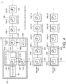
- FIG. 4 is a schematic diagram illustrating functions of the timers in configuration example 1 of the control system 1 according to this embodiment.
- the communication control circuit 110 of the CPU unit 100 includes the timer 114 which functions as a grand master clock.
- the timer 114 since the communication control circuit 110 and the NIC 120 are mounted on the same SOC 101, the timer 114 also functions as a timer 124 of the NIC 120. That is, the timer 124 of the NIC 120 is virtual and an entity thereof is the same as the timer 114 of the communication control circuit 110. Accordingly, the timer 114 of the communication control circuit 110 functions as a boundary clock of the field network 3.
- the timer 134 of the bus master circuit 130 functions as a boundary clock of the local bus 2 and is time-synchronized with the timer 114 of the communication control circuit 110 functioning as the grand master clock.
- a synchronization function 116 is mounted in the timer 114 of the communication control circuit 110 and a latch function 138 is mounted in the timer 134 of the bus master circuit 130.
- the timer 114 asserts a synchronization signal at a designated time
- the synchronization function 116 of the timer 114 notifies of the time at which the synchronization signal is asserted.
- the latch function 138 sets a difference between the time (which is held by the bus master circuit 130) and the previously notified time as a time correction value in the timer 134.
- FIG. 5 is a sequence diagram illustrating an example of a time synchronization procedure between the timer 114 of the communication control circuit 110 and the timer 134 of the bus master circuit 130 in configuration example 1 of the control system 1 according to this embodiment.
- the processor 102, the timer 114 of the communication control circuit 110, and the timer 134 of the bus master circuit 130 cooperate with each other to realize time synchronization between the timer 114 of the communication control circuit 110 and the timer 134 of the bus master circuit 130.
- each of the timer 114 and the timer 134 includes a free-run counter and a logic that calculates a local time from a counter value output from the free-run counter.
- the timer 114 of the communication control circuit 110 asserts a synchronization signal (hereinafter also abbreviated to "SYNC") every predetermined cycle designated by the processor 102.
- the timer 134 of the bus master circuit 130 calculates a difference between the reference clock and the free-run counter of the timer 134 on the basis of the synchronization signal and sequentially corrects the free-run counter. An upper limit of a correction value per time for the free-run counter is determined.
- the timer 134 of the bus master circuit 130 notifies the timer 114 of the communication control circuit 110 of time synchronization end.
- the notification of time synchronization end may be performed by interruption.
- the processor 102 sets an output cycle of a synchronization signal for the timer 114 of the communication control circuit 110 (Sequence SQ100).
- the processor 102 sets a necessary initial value for the timer 134 of the bus master circuit 130 and sets a state register indicating an asynchronous state (Sequence SQ102).
- Sequence SQ102 may be realized by setting or changing a register value held by the bus master circuit 130.
- the processor 102 sets the timer 114 of the communication control circuit 110 such that a synchronization signal is output to the timer 134 of the bus master circuit 130 every predetermined cycle designated in advance.
- the processor 102 reads the value of the free-run counter included in the timer 114 of the communication control circuit 110 (Sequence SQ104) and acquires a current counter value of the free-run counter (Sequence SQ106). Then, the processor 102 notifies the timer 134 of the bus master circuit 130 of the local time of the timer 114 (Sequence SQ108). This notification is a part of the time synchronization function and the processor 102 notifies the timer 134 of the bus master circuit 130 of the local time in the timer 114 of the communication control circuit 110 indicating a time at which the synchronization signal set is output and which is set in the timer 114 of the communication control circuit 110. The timer 114 sequentially corrects the free-run counter on the basis of a difference between a scheduled time at which the first synchronization signal is asserted and the local time at which the synchronization signal is actually detected.
- the processor 102 notifies the timer 134 of the bus master circuit 130 of the (scheduled) time at which the first synchronization signal is asserted (Sequence SQ110). That is, in Sequence SQ112 which will be described later, the timer 114 is instructed to start output of the synchronization signal, and the timer 134 is notified of the scheduled time at which the first synchronization signal will be output and which is counted from the time at which the output start is instructed.
- the processor 102 sets an output start time of the synchronization signal (SYNTIME1) and a synchronization start command for the timer 114 (Sequence SQ112).
- the timer 114 validates the output of the synchronization signal and counts up to designated SYNTIME1 in response to this setting, the timer asserts the synchronization signal to the timer 134 (Sequence SQ116). Since the timer 114 repeatedly asserts the synchronization signal at a designated output cycle (SCYCLE1) while the output of the synchronization signal is validated, SCYCLE1 is added to SYNTIME1 to calculate new SYNTIME1 (SYNTIME1 ⁇ SYNTIME1+SCYCLE1). FIG. 13 and the like will be referred to for details of new SYNTIME1.
- the timer 134 performs time correction by correcting the free-run counter on the basis of a difference from the output start time (SYNTIME1) of the synchronization signal and a difference from the local time at which the output cycle from the timer 114 is detected (Sequence SQ118). In this way, the timer 134 is subjected to time correction on the basis of the difference between the time (the local time) in the timer 134 at which the synchronization signal output from the timer 114 of the communication control circuit 110 is detected by the timer 134 of the bus master circuit 130 and the scheduled time at which the synchronization signal is asserted and which has been notified of in advance.
- Sequences SQ114 to SQ118 are repeated until the correction value in Sequence SQ118 is equal to or less than a predetermined value.
- the upper limit of the correction value for the free-run counter may be set in advance.
- the timer 134 When the correction value is equal to or less than the predetermined value and it is determined that synchronization of the timer 134 is completed, the timer 134 notifies the timer 114 of time synchronization end (Sequence SQ122).
- the notification of time synchronization end is performed by interruption from the timer 134 to the timer 114.
- the timer 114 reads the state register of the timer 134 (Sequence SQ124) and acquires the value of the state register of the timer 134 (Sequence SQ126). Then, the timer 114 notifies the processor 102 of the acquired value of the state register of the timer 134 (Sequence SQ128).
- the processor 102 When the value of the state register of the timer 134 is detected from the timer 114, the processor 102 reads the state register of the timer 134 (Sequence SQ130) and acquires the value of the state register of the timer 134 (Sequence SQ132). Then, when the value of the state register notified of in Sequence SQ128 matches the value of the state register acquired in Sequence SQ132, the processor 102 clears the state register of the timer 134 (Sequence SQ134).
- time synchronization between the timer 114 of the communication control circuit 110 and the timer 134 of the bus master circuit 130 is realized.
- time synchronization is realized again by repeatedly performing the processes of Sequences SQ114 to SQ118.
- times of various processes or control can be synchronized between the configurations according to a plurality of protocols which are provided in the same CPU unit 100.
- timer 114 of the communication control circuit 110 functions as a grand master clock
- the timer 114 of the communication control circuit 110 may be time-synchronized with another clock.
- the other clock functions as a grand master clock.
- the timer 304 of the external device 300 connected to the CPU unit 100 in the control system 1 illustrated in FIG. 1 functions as a grand master clock
- FIG. 6 is a schematic diagram illustrating functions of the timers in configuration example 2 of the control system 1 according to this embodiment.
- an external device 300 is connected to the CPU unit 100 and the external device 300 includes a timer 304 which functions as a grand master clock.
- the timer 304 of the external device 300 is a reference clock of the timer 114 of the communication control circuit 110. That is, the timer 114 of the communication control circuit 110 functions as a boundary clock of the field network 3 and is synchronized with the timer 304 of the external device 300 functioning as a grand master clock.
- the timer 134 of the bus master circuit 130 functions as a boundary clock of the local bus 2 and is synchronized with the timer 114 of the communication control circuit 110 functioning as the boundary clock.
- the time synchronization procedure between the timer 134 of the bus master circuit 130 and the timer 114 of the communication control circuit 110 is the same as described in configuration example 1 of the control system and detailed description thereof will not be repeated.
- the external device 300 has the same function as the NIC 120 of the CPU unit 100 and functions as a communication master of the field network 5.
- An arbitrary slave device 310 may be connected to the field network 5.
- the slave device 310 connected to the field network 5 time-synchronizes the timer 314 thereof with the timer 304 of the external device 300.
- FIG. 7 is a schematic diagram illustrating principal parts of the CPU unit 100 and the external device 300 illustrated in FIG. 6 .
- a latch function 118 is provided in the timer 114 of the communication control circuit 110 and a synchronization function 306 is provided in the timer 304 of the external device 300.
- the latch function 118 of the timer 114 latches the local time at which a synchronization signal (SYNC) input from the external device 300 is asserted.
- Time correction for the timer 114 is performed on the basis of a difference between the time at which the external device 300 asserts the synchronization signal and the time at which the timer 114 of the communication control circuit 110 detects the synchronization signal.
- FIG. 8 is a sequence diagram illustrating an example of a time synchronization procedure between the timer 304 of the external device 300 and the timer 114 of the communication control circuit 110 in configuration example 2 of the control system 1 according to this embodiment.
- the timer 304 of the external device 300, the processor 102, and the timer 114 of the communication control circuit 110 cooperate with each other to realize time synchronization between the timer 304 of the external device 300 and the timer 114 of the communication control circuit 110. It is assumed that each of the timer 304 and the timer 114 includes a free-run counter and a logic that calculates a local time from a counter value output from the free-run counter.
- the timer 304 of the external device 300 asserts a synchronization signal (SYNC) at a trigger time (TRGTTML) which is designated by the processor 102.
- the latch function 118 of the timer 114 latches a local time (hereinafter also referred to as a "latch time") at which the synchronization signal (SYNC) input from the external device 300 is detected.
- Time correction for the timer 114 is performed on the basis of a difference (a time difference value) between the trigger time at which the synchronization signal is asserted by the external device 300 and the latch time at which the local time is latched by the latch function 118 of the timer 114 of the communication control circuit 110.
- the processor 102 performs necessary initial setting for the timer 304 of the external device 300 (Sequence SQ200).
- the initial setting includes setting of a time (a trigger time) at which a synchronization signal is first generated. That is, as a part of the time synchronization function, the processor 102 sets the timer 304 of the external device 300 such that the synchronization signal is output to the timer 114 of the communication control circuit 110 at the designated trigger time.
- the processor 102 performs initial setting of a parameter for correcting a detection error due to a noise filter for the timer 114 of the communication control circuit 110 (Sequence SQ202). This correction of the detection error will be described in detail later.
- the correction of the detection error is necessary when a noise filter is provided in the latch function 118 of the timer 114, and the process of Sequence SQ202 may be skipped when a noise filter is not provided.
- the timer 304 of the external device 300 When the timer 304 of the external device 300 counts up to the designated trigger time, the timer 304 asserts a synchronization signal to the timer 114 (Sequence SQ206). When the synchronization signal asserted by the timer 304 of the external device 300 is detected, the timer 114 latches the local time indicating the detection time in a register.
- the processor 102 After the synchronization signal is asserted, the processor 102 generates an internal trigger thereof (Sequence SQ208), reads a value of the local time (the latch time) latched in the register of the timer 114 of the communication control circuit 110 (Sequence SQ210), and acquires the latch time (Sequence SQ212). In this way, as a part of the time synchronization function, the processor 102 reads the local time (the latch time) in the timer 114, which is stored when the synchronization signal output from the timer 304 of the external device 300 is detected by the timer 114 of the communication control circuit 110, from the timer 114.
- the processor 102 calculates a difference (a time difference value) between the trigger time and the acquired latch time and writes the time difference value to the register of the timer 114 (Sequence SQ214). Then, the timer 114 of the communication control circuit 110 performs time correction on the basis of the time difference value written to the register thereof (Sequence SQ216). In this way, as a part of the time synchronization function, the processor 102 instructs the timer 114 to perform the time correction on the basis of the difference between the time (the trigger time) at which the synchronization signal is generated and the local time (the latch time) in the timer 114 which is stored when the synchronization signal is detected by the timer 114.
- the processor 102 sets a time (a trigger time) at which a synchronization signal will be generated next for the timer 304 of the external device 300 (Sequence SQ218).
- the processes of Sequences SQ204 to SQ218 are repeated until the correction value in Sequence SQ216 is equal to or less than the predetermined value.
- the time synchronization between the timer 304 of the external device 300 and the timer 114 of the communication control circuit 110 is realized.
- the time synchronization between the timer 304 of the external device 300 and the timer 114 of the communication control circuit 110 is not achieved, the time synchronization is realized again by repeatedly performing the processes of SQ204 to SQ218.
- an arbitrary reference clock can be newly provided in one or more existing configurations according to a protocol and then the entire control system 1 can be synchronized with the reference clock.
- a method of correcting a detection error due to a noise filter when the noise filter is provided in the latch function 118 of the timer 114 of the communication control circuit 110 will be described below.
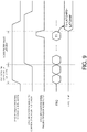
- FIG. 9 is a schematic diagram illustrating a method of correcting a detection error in a case in which a noise filter is provided in a latch function of a timer.
- the noise filter of the latch function of the timer is defined by a noise filter value (LATCHNF).
- LATCHNF noise filter value
- a time that is, a latch time which will be originally stored
- Original latch time counter value T 1 ⁇ propagation delay value LATCHPD ⁇ noise filter value LATCHNF
- Sequence SQ206 illustrated in FIG. 8 when the timer 304 of the external device 300 asserts the synchronization signal to the timer 114 of the communication control circuit 110, the timer 114 acquires the counter value T1 of the free-run counter therein at a time at which the synchronization signal passing through the noise filter varies, and stores a value obtained by subtracting a propagation delay value (LATCHPD) and a noise filter value (LATCHNF) from the acquired counter value T1 as a latch time in a register.
- LATCHPD propagation delay value
- LATCHNF noise filter value
- the processor 102 having the time synchronization function provides setting for the noise filter included in the timer 114.
- the timer 114 compensates for a time delay which is generated due to the noise filter on the basis of setting for the noise filter and then stores (latches) the latch time.
- timer 304 of the external device 300 functions as a grand master clock
- timer 114 of the communication control circuit 110 may function as a grand master clock for the timer 304 of the external device 300.
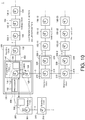
- FIG. 10 is a schematic diagram illustrating functions of timers in configuration example 3 of the control system 1 according to this embodiment.
- Configuration example 3 illustrated in FIG. 10 is the same as configuration example 2 illustrated in FIG. 6 , except that the timer 114 of the communication control circuit 110 functions as a grand master clock and the timer 304 of the external device 300 functions as a boundary clock. That is, in configuration example 3 illustrated in FIG. 10 , the timer 304 of the external device 300 outside the CPU unit 100 in addition to the timer 134 of the bus master circuit 130 in the CPU unit 100 is time-synchronized with the timer 114 of the communication control circuit 110 as a reference clock.
- the timer 314 of the slave device 310 connected to the field network 5 is time-synchronized with the timer 304 of the external device 300 as a reference clock.
- functional units connected to the CPU unit 100 via other communication means as well as the functional units 150 connected to the CPU unit 100 via a local bus or a field network can be time-synchronized.
- FIG. 11 is a schematic diagram illustrating principal parts of the CPU unit 100 and the external device 300 illustrated in FIG. 10 .
- the synchronization function 116 is provided in the timer 114 of the communication control circuit 110 and the latch function 308 is provided in the timer 304 of the external device 300.
- the synchronization function 116 of the timer 114 asserts a synchronization signal (SYNC) every predetermined cycle.
- Time correction on the timer 304 is performed on the basis of a difference between the time at which the timer 114 of the communication control circuit 110 asserts the synchronization signal and the time at which the timer 304 of the external device 300 detects the synchronization signal.
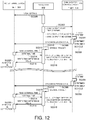
- FIG. 12 is a sequence diagram illustrating an example of a time synchronization procedure between the timer 114 of the communication control circuit 110 and the timer 304 of the external device 300 in configuration example 3 of the control system 1 according to this embodiment.
- the timer 304 of the external device 300, the processor 102, and the timer 114 of the communication control circuit 110 cooperate with each other to realize time synchronization between the timer 114 of the communication control circuit 110 and the timer 304 of the external device 300.
- each of the timer 114 and the timer 304 includes a free-run counter and a logic that calculates a local time from a counter value output from the free-run counter.
- the timer 114 of the communication control circuit 110 asserts a synchronization signal (SYNC) every predetermined cycle (that is, an output period of a synchronization signal (SCYCLE)) designated by the processor 102.
- the latch function 308 of the external device 300 latches a local time (hereinafter also referred to as an "external time") at which the synchronization signal (SYNC) input from the communication control circuit 110 is detected.
- Time correction on the timer 304 is performed on the basis of a difference (a time difference value) between the external time which is latched by the latch function 308 of the timer 304 of the external device 300 and the output start time at which the synchronization signal is asserted by the communication control circuit 110.
- the processor 102 performs necessary initial setting on the timer 304 of the external device 300 (Sequence SQ300).
- the processor 102 sets the output start time (SYNTIME) of the synchronization signal, the output cycle (SCYCLE) of the synchronization signal, and the output time (SATIME) of the synchronization signal as parameters required for the time synchronization for the timer 114 of the communication control circuit 110 (Sequence SQ302).
- FIG. 13 is a timing chart illustrating a relationship between parameters set in sequence SQ302 in FIG. 12 and an asserted synchronization signal.
- a first synchronization signal is asserted at the output start time (SYNTIME). Asserting of the synchronization signal is continuously performed for the output time (SATIME) from the output start time. Then, when a next cycle arrives, that is, when a next output cycle (SYNTIME ⁇ SYNTIME + SCYCLE) arrives, a next synchronization signal is asserted. In a period of the output cycle (SCYCLE) from which the output time (SATIME) is excluded, the synchronization function is deactivated.
- the timer 114 of the communication control circuit 110 when the timer 114 of the communication control circuit 110 counts up to the designated output start time (SYNTIME) (Sequence SQ304), the timer 114 asserts the synchronization signal to the timer 304 (Sequence SQ306).
- the timer 304 latches a local time (an external time) indicating the detected time in a register.
- the timer 114 of the communication control circuit 110 calculates the output start time of the next cycle (Sequence SQ308).
- the processor 102 After the synchronization signal is asserted, the processor 102 generates an internal trigger thereof (Sequence SQ310), reads a value of the local time (the external time) latched in the register of the timer 304 of the external device 300 (Sequence SQ312), and acquires the external time (Sequence SQ314). Then, the processor 102 calculates a difference (a time difference value) between the acquired external time and the output start time (Sequence SQ316) and writes the time difference value to the register of the timer 304 (Sequence SQ318). Then, the timer 304 of the external device 300 performs time correction on the basis of the time difference value written to the register thereof (Sequence SQ320).
- Sequences SQ304 to SQ320 are repeated until the correction value in Sequence SQ320 is equal to or less than a predetermined value.
- the time synchronization between the timer 114 of the communication control circuit 110 and the timer 304 of the external device 300 is realized.
- the time synchronization is realized again by repeatedly performing the processes of Sequences SQ304 to SQ320.
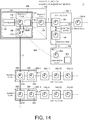
- FIG. 14 is a schematic diagram illustrating functions of timers in configuration example 4 of the control system 1 according to this embodiment.
- the external device 300 is connected subordinate to the functional unit 150-1.
- the functional unit 150-1 includes another timer 156 functioning as a boundary clock of a field network 6 for connection of the external device 300 in addition to the control logic 152 and the timer 154.
- the timer 304 of the external device 300 is a reference clock of the timer 114 of the communication control circuit 110. That is, the timer 114 of the communication control circuit 110 is synchronized with the timer 304 of the external device 300 functioning as a grand master clock.
- a latch function 118 is provided in the timer 114 of the communication control circuit 110 and a synchronization function 306 is provided in the timer 304 of the external device 300.
- the external device 300 is connected to the CPU unit 100 via entities (the functional units 150-1, 150-2, ...) which transmit and receive data to and from the bus master circuit 130. Since the timer 114 of the communication control circuit 110 of the CPU unit 100 is connected to the timer 304 of the external device 300 via the local bus 2, the functional unit 150-1, and the field network 6, time synchronization between the timer 114 of the communication control circuit 110 and the timer 134 of the bus master circuit 130 is realized by performing the time synchronization procedures illustrated in FIGs. 8 and 12 in combination. The time synchronization procedures are the same as described above in detail and thus description thereof will not be repeated here.
- FIG. 15 is a schematic diagram illustrating functions of timers in configuration example 5 of the control system 1 according to this embodiment.
- the external device 300 is connected subordinate to the functional unit 150-11.
- the functional unit 150-11 includes another timer 156 functioning as a boundary clock of a field network 7 for connection of the external device 300 in addition to the control logic 152 and the timer 154.
- the timer 304 of the external device 300 is a reference clock of the timer 114 of the communication control circuit 110. That is, the timer 114 of the communication control circuit 110 is synchronized with the timer 304 of the external device 300 functioning as a grand master clock.
- a latch function 118 is provided in the timer 114 of the communication control circuit 110 and a synchronization function 306 is provided in the timer 304 of the external device 300.
- the external device 300 is connected to the CPU unit 100 via entities (the functional units 150-11, 150-12, ...) which transmit and receive data to and from the NIC 120. Since the timer 114 of the communication control circuit 110 of the CPU unit 100 is connected to the timer 304 of the external device 300 via the field network 3, the communication coupler unit 200-1, the local bus 4-1, the functional unit 150-11, and the field network 7, time synchronization between the timer 114 of the communication control circuit 110 and the timer 134 of the bus master circuit 130 is realized by performing the time synchronization procedures illustrated in FIGs. 8 and 12 in combination. The time synchronization procedures are the same as described above in detail and thus description thereof will not be repeated here.
- configuration examples 5 and 6 of the control system 1 a configuration in which the timer 304 of the external device 300 functions as a grand master clock has been described above, but the timer 114 of the communication control circuit 110 may function as a grand master clock for the timer 304 of the external device 300 as described in configuration example 3 (see FIG. 10 and the like) of the control system 1. That is, the timer 304 of the external device 300 may use the timer 114 of the communication control circuit 110 as a reference clock.
- This configuration is the same as in configuration example 3 and thus detailed description thereof will not be repeated.
- the present invention is applied to the control system 1 for controlling machines or facilities, but the present invention can be applied to a general network configuration.
- An example of such a network configuration is a configuration in which guaranteeing of a transmission time of data or an arrival time is required such as a higher network connected to a plurality of PLCs.
- Applications of the present invention are not limited to such configurations.
- control system 1 since communication means according to different protocols can be time-synchronized with each other, it is possible to realize time synchronization of an entire control system without depending on protocols of buses or networks used to connect the CPU unit and the functional units. Accordingly, it is possible to synchronize input times and/or output times of a plurality of slave units (typically, functional units) connected to the communication means according to different protocols and to enhance control accuracy.
- slave units typically, functional units
- a clock functioning as a grand master clock can be provided in an arbitrary device or unit. Accordingly, for example, even when a new CPU unit, a new functional unit, or the like is added to an existing control system, it is possible to easily realize time synchronization between the existing system and the new system. Accordingly, even when modifications such as certain additions or alternations are applied to an existing control system, it is possible to maintain time synchronization of the system as a whole. Accordingly, even when an existing control system is extended or a plurality of control systems are newly constructed, it is possible to develop a control system with a higher degree of freedom without considering a particular idea for achieving time synchronization.
Landscapes
- Engineering & Computer Science (AREA)
- Theoretical Computer Science (AREA)
- Computer Networks & Wireless Communication (AREA)
- Signal Processing (AREA)
- General Engineering & Computer Science (AREA)
- Physics & Mathematics (AREA)
- General Physics & Mathematics (AREA)
- Quality & Reliability (AREA)
- Automation & Control Theory (AREA)
- Manufacturing & Machinery (AREA)
- Computer Security & Cryptography (AREA)
- Synchronisation In Digital Transmission Systems (AREA)
- Small-Scale Networks (AREA)
Applications Claiming Priority (1)
| Application Number | Priority Date | Filing Date | Title |
|---|---|---|---|
| JP2016202215A JP6753262B2 (ja) | 2016-10-14 | 2016-10-14 | 制御装置および通信装置 |
Publications (2)
| Publication Number | Publication Date |
|---|---|
| EP3309647A1 true EP3309647A1 (de) | 2018-04-18 |
| EP3309647B1 EP3309647B1 (de) | 2024-01-03 |
Family
ID=60001653
Family Applications (1)
| Application Number | Title | Priority Date | Filing Date |
|---|---|---|---|
| EP17191562.2A Active EP3309647B1 (de) | 2016-10-14 | 2017-09-18 | Steuerungsvorrichtung und kommunikationsvorrichtung |
Country Status (4)
| Country | Link |
|---|---|
| US (1) | US10284692B2 (de) |
| EP (1) | EP3309647B1 (de) |
| JP (1) | JP6753262B2 (de) |
| CN (1) | CN107959564A (de) |
Families Citing this family (20)
| Publication number | Priority date | Publication date | Assignee | Title |
|---|---|---|---|---|
| JP6399136B1 (ja) * | 2017-03-31 | 2018-10-03 | オムロン株式会社 | 制御装置、制御プログラム、および制御システム |
| JP7143697B2 (ja) * | 2018-09-14 | 2022-09-29 | オムロン株式会社 | 制御システムおよび制御装置 |
| CN112703705A (zh) * | 2018-09-21 | 2021-04-23 | 三菱电机株式会社 | 通信装置、通信系统、通信方法及通信程序 |
| WO2020059138A1 (ja) | 2018-09-21 | 2020-03-26 | 三菱電機株式会社 | 通信装置、通信システム、通信方法および通信プログラム |
| JP7484912B2 (ja) * | 2019-07-04 | 2024-05-16 | オムロン株式会社 | 制御システム |
| JP7251402B2 (ja) * | 2019-08-20 | 2023-04-04 | オムロン株式会社 | 制御システム、制御装置およびプログラム |
| CN113542090B (zh) * | 2020-04-14 | 2023-07-14 | 宁波弘讯科技股份有限公司 | 一种EtherCAT主从站一体网桥控制器及控制方法 |
| US11860688B1 (en) * | 2020-04-28 | 2024-01-02 | T-Mobile Innovations Llc | Network generated precision time |
| CN112564841B (zh) * | 2020-12-08 | 2025-02-18 | 深圳市软赢科技有限公司 | 通过同步时钟的方式控制不同通讯协议的设备的方法 |
| WO2022168475A1 (ja) * | 2021-02-04 | 2022-08-11 | オムロン株式会社 | 制御装置 |
| WO2022168338A1 (ja) * | 2021-02-04 | 2022-08-11 | オムロン株式会社 | 制御装置 |
| CN113534887B (zh) * | 2021-05-25 | 2024-06-14 | 交控科技股份有限公司 | 基于实时总线的板卡间时间同步方法、装置和电子设备 |
| JP7682716B2 (ja) * | 2021-06-25 | 2025-05-26 | キヤノン株式会社 | 通信装置 |
| JP7724730B2 (ja) * | 2022-02-24 | 2025-08-18 | 三菱電機株式会社 | 基準パルス補正装置及び基準パルス補正方法 |
| JP2024075064A (ja) * | 2022-11-22 | 2024-06-03 | キヤノン株式会社 | 通信装置、通信装置の制御方法、およびプログラム |
| WO2024197421A1 (en) * | 2023-03-29 | 2024-10-03 | 7980302 Canada Inc. | Safe vehicle speed limiter |
| CN120898398A (zh) * | 2023-04-11 | 2025-11-04 | 三菱电机株式会社 | 通信设备、时刻同步系统、时刻同步方法以及程序 |
| WO2025197503A1 (ja) * | 2024-03-21 | 2025-09-25 | ソニーグループ株式会社 | 通信装置、ロボットの通信方法、及び、ロボット |
| EP4660724A1 (de) * | 2024-06-04 | 2025-12-10 | Siemens Aktiengesellschaft | Verfahren zum bereitstellen einer sicheren zeitbasis für ein steuerprogramm |
| EP4682648A1 (de) * | 2024-07-18 | 2026-01-21 | Siemens Aktiengesellschaft | Verfahren zum betreiben einer zyklusorientierten steuerungs-software |
Citations (3)
| Publication number | Priority date | Publication date | Assignee | Title |
|---|---|---|---|---|
| US20130173950A1 (en) * | 2012-01-04 | 2013-07-04 | Marvell World Trade Ltd. | Method and apparatus for communicating time information between time aware devices |
| JP2014120884A (ja) | 2012-12-14 | 2014-06-30 | Omron Corp | 情報処理装置、情報処理プログラムおよび情報処理方法 |
| US20160292110A1 (en) * | 2015-03-31 | 2016-10-06 | Omron Corporation | Information processing apparatus, information processing program, and information processing method |
Family Cites Families (15)
| Publication number | Priority date | Publication date | Assignee | Title |
|---|---|---|---|---|
| JPH10124465A (ja) * | 1996-10-16 | 1998-05-15 | Fuji Xerox Co Ltd | 情報処理装置 |
| US6944247B2 (en) * | 1999-11-19 | 2005-09-13 | Texas Instruments Incorporated | Plural circuit selection using role reversing control inputs |
| CN1308940C (zh) * | 2003-09-24 | 2007-04-04 | 松下电器产业株式会社 | 伺服误差信号生成电路以及伺服误差信号生成方法 |
| DE102005061155A1 (de) * | 2005-12-21 | 2007-06-28 | Bosch Rexroth Ag | Kommunikationsstruktur |
| US8072858B2 (en) * | 2006-01-27 | 2011-12-06 | Panasonic Corporation | Optical disk apparatus, control method of optical disk apparatus, and integrated circuit |
| US8160447B2 (en) * | 2007-10-17 | 2012-04-17 | Hitachi, Ltd. | Communication system using passive optical network and passive optical network |
| TWI411277B (zh) * | 2009-12-23 | 2013-10-01 | Ind Tech Res Inst | 網路從節點與網路系統精確時間同步之方法 |
| WO2012118178A1 (ja) * | 2011-03-03 | 2012-09-07 | 日本電気株式会社 | 同期システム、同期方法、第一の同期装置、第二の同期装置及びコンピュータプログラム |
| CN102624514B (zh) * | 2012-03-01 | 2015-03-25 | 江苏中兴微通信息科技有限公司 | 一种提高无线信道测量的定时同步精度的方法 |
| JP5911601B2 (ja) * | 2012-11-28 | 2016-04-27 | 三菱電機株式会社 | 通信装置、通信システムおよび時刻同期方法 |
| JP6193009B2 (ja) * | 2013-06-21 | 2017-09-06 | 株式会社東芝 | 無線通信装置及び無線通信システム |
| JP6191480B2 (ja) * | 2014-01-30 | 2017-09-06 | 横河電機株式会社 | データ収集システム |
| JP2014096853A (ja) * | 2014-02-13 | 2014-05-22 | Mitsubishi Electric Corp | 時刻同期装置 |
| KR101542016B1 (ko) * | 2014-09-17 | 2015-08-05 | 성균관대학교산학협력단 | 차량 내 이종 네트워크 도메인들 간의 동기화 게이트웨이 장치 및 동기화 방법 |
| JP6381392B2 (ja) * | 2014-09-30 | 2018-08-29 | Kddi株式会社 | Ponシステム、olt、onuおよび伝送方法 |
-
2016
- 2016-10-14 JP JP2016202215A patent/JP6753262B2/ja active Active
-
2017
- 2017-09-18 EP EP17191562.2A patent/EP3309647B1/de active Active
- 2017-09-19 US US15/708,146 patent/US10284692B2/en active Active
- 2017-09-21 CN CN201710862684.XA patent/CN107959564A/zh active Pending
Patent Citations (3)
| Publication number | Priority date | Publication date | Assignee | Title |
|---|---|---|---|---|
| US20130173950A1 (en) * | 2012-01-04 | 2013-07-04 | Marvell World Trade Ltd. | Method and apparatus for communicating time information between time aware devices |
| JP2014120884A (ja) | 2012-12-14 | 2014-06-30 | Omron Corp | 情報処理装置、情報処理プログラムおよび情報処理方法 |
| US20160292110A1 (en) * | 2015-03-31 | 2016-10-06 | Omron Corporation | Information processing apparatus, information processing program, and information processing method |
Also Published As
| Publication number | Publication date |
|---|---|
| EP3309647B1 (de) | 2024-01-03 |
| US20180109655A1 (en) | 2018-04-19 |
| US10284692B2 (en) | 2019-05-07 |
| JP6753262B2 (ja) | 2020-09-09 |
| JP2018064219A (ja) | 2018-04-19 |
| CN107959564A (zh) | 2018-04-24 |
Similar Documents
| Publication | Publication Date | Title |
|---|---|---|
| EP3309647B1 (de) | Steuerungsvorrichtung und kommunikationsvorrichtung | |
| EP1757410B1 (de) | Verfahren und System zur koordinierten Steuerung von Robotern | |
| US9398080B2 (en) | Control device, image processing device, control method, computer-readable recording medium, and program | |
| US7383458B2 (en) | Method and device for synchronizing the cycle time of a plurality of TTCAN buses based on determined global time deviations and corresponding bus system | |
| US11307553B2 (en) | Control device and control method | |
| Hartwich et al. | CAN network with time triggered communication | |
| WO2015128981A1 (ja) | プログラマブルコントローラシステム、そのコントローラ | |
| US11310026B2 (en) | Communication system, communication device, and program | |
| KR20030084984A (ko) | 버스 시스템의 적어도 하나의 노드의 동기화를 위한 방법및 장치 및 이에 상응하는 버스 시스템 | |
| US9698933B2 (en) | Communication device and communication method | |
| WO2018070190A1 (ja) | 演算装置および制御システム | |
| US7200766B2 (en) | Method and system for the distributed synchronization of users of a communications link | |
| JP6400553B2 (ja) | ユニット間での同期制御機能を有する数値制御システム | |
| WO2023026431A1 (ja) | 通信制御装置、通信制御方法及びプログラム | |
| JP2007050812A (ja) | 負荷制御システム、通信制御ユニットおよび負荷制御方法 | |
| CN108541307B (zh) | 可编程控制器以及同步控制方法 | |
| JP6205930B2 (ja) | 受信装置及び通信システム | |
| US20250189954A1 (en) | Field bus system | |
| US11294421B2 (en) | Precision timing between systems | |
| JP2024011842A (ja) | 情報通信システム及び情報通信装置 | |
| JP2014222847A (ja) | 通信システム | |
| CN111193509A (zh) | 源同步数据采样点自动校准方法及系统 | |
| US20200204537A1 (en) | Relay apparatus, relay method, and computer readable medium | |
| JP2010020389A (ja) | 半導体装置、半導体システム、および、同期化方法 |
Legal Events
| Date | Code | Title | Description |
|---|---|---|---|
| PUAI | Public reference made under article 153(3) epc to a published international application that has entered the european phase |
Free format text: ORIGINAL CODE: 0009012 |
|
| STAA | Information on the status of an ep patent application or granted ep patent |
Free format text: STATUS: REQUEST FOR EXAMINATION WAS MADE |
|
| 17P | Request for examination filed |
Effective date: 20170918 |
|
| AK | Designated contracting states |
Kind code of ref document: A1 Designated state(s): AL AT BE BG CH CY CZ DE DK EE ES FI FR GB GR HR HU IE IS IT LI LT LU LV MC MK MT NL NO PL PT RO RS SE SI SK SM TR |
|
| AX | Request for extension of the european patent |
Extension state: BA ME |
|
| RBV | Designated contracting states (corrected) |
Designated state(s): AL AT BE BG CH CY CZ DE DK EE ES FI FR GB GR HR HU IE IS IT LI LT LU LV MC MK MT NL NO PL PT RO RS SE SI SK SM TR |
|
| STAA | Information on the status of an ep patent application or granted ep patent |
Free format text: STATUS: EXAMINATION IS IN PROGRESS |
|
| 17Q | First examination report despatched |
Effective date: 20190508 |
|
| GRAP | Despatch of communication of intention to grant a patent |
Free format text: ORIGINAL CODE: EPIDOSNIGR1 |
|
| STAA | Information on the status of an ep patent application or granted ep patent |
Free format text: STATUS: GRANT OF PATENT IS INTENDED |
|
| INTG | Intention to grant announced |
Effective date: 20230810 |
|
| GRAS | Grant fee paid |
Free format text: ORIGINAL CODE: EPIDOSNIGR3 |
|
| GRAA | (expected) grant |
Free format text: ORIGINAL CODE: 0009210 |
|
| STAA | Information on the status of an ep patent application or granted ep patent |
Free format text: STATUS: THE PATENT HAS BEEN GRANTED |
|
| AK | Designated contracting states |
Kind code of ref document: B1 Designated state(s): AL AT BE BG CH CY CZ DE DK EE ES FI FR GB GR HR HU IE IS IT LI LT LU LV MC MK MT NL NO PL PT RO RS SE SI SK SM TR |
|
| REG | Reference to a national code |
Ref country code: GB Ref legal event code: FG4D |
|
| REG | Reference to a national code |
Ref country code: CH Ref legal event code: EP |
|
| REG | Reference to a national code |
Ref country code: DE Ref legal event code: R096 Ref document number: 602017078071 Country of ref document: DE |
|
| REG | Reference to a national code |
Ref country code: IE Ref legal event code: FG4D |
|
| REG | Reference to a national code |
Ref country code: LT Ref legal event code: MG9D |
|
| PG25 | Lapsed in a contracting state [announced via postgrant information from national office to epo] |
Ref country code: ES Free format text: LAPSE BECAUSE OF FAILURE TO SUBMIT A TRANSLATION OF THE DESCRIPTION OR TO PAY THE FEE WITHIN THE PRESCRIBED TIME-LIMIT Effective date: 20240103 |
|
| PG25 | Lapsed in a contracting state [announced via postgrant information from national office to epo] |
Ref country code: ES Free format text: LAPSE BECAUSE OF FAILURE TO SUBMIT A TRANSLATION OF THE DESCRIPTION OR TO PAY THE FEE WITHIN THE PRESCRIBED TIME-LIMIT Effective date: 20240103 |
|
| REG | Reference to a national code |
Ref country code: NL Ref legal event code: MP Effective date: 20240103 |
|
| REG | Reference to a national code |
Ref country code: AT Ref legal event code: MK05 Ref document number: 1647458 Country of ref document: AT Kind code of ref document: T Effective date: 20240103 |
|
| PG25 | Lapsed in a contracting state [announced via postgrant information from national office to epo] |
Ref country code: NL Free format text: LAPSE BECAUSE OF FAILURE TO SUBMIT A TRANSLATION OF THE DESCRIPTION OR TO PAY THE FEE WITHIN THE PRESCRIBED TIME-LIMIT Effective date: 20240103 |
|
| PG25 | Lapsed in a contracting state [announced via postgrant information from national office to epo] |
Ref country code: NL Free format text: LAPSE BECAUSE OF FAILURE TO SUBMIT A TRANSLATION OF THE DESCRIPTION OR TO PAY THE FEE WITHIN THE PRESCRIBED TIME-LIMIT Effective date: 20240103 |
|
| PG25 | Lapsed in a contracting state [announced via postgrant information from national office to epo] |
Ref country code: IS Free format text: LAPSE BECAUSE OF FAILURE TO SUBMIT A TRANSLATION OF THE DESCRIPTION OR TO PAY THE FEE WITHIN THE PRESCRIBED TIME-LIMIT Effective date: 20240503 |
|
| PG25 | Lapsed in a contracting state [announced via postgrant information from national office to epo] |
Ref country code: LT Free format text: LAPSE BECAUSE OF FAILURE TO SUBMIT A TRANSLATION OF THE DESCRIPTION OR TO PAY THE FEE WITHIN THE PRESCRIBED TIME-LIMIT Effective date: 20240103 |
|
| PG25 | Lapsed in a contracting state [announced via postgrant information from national office to epo] |
Ref country code: GR Free format text: LAPSE BECAUSE OF FAILURE TO SUBMIT A TRANSLATION OF THE DESCRIPTION OR TO PAY THE FEE WITHIN THE PRESCRIBED TIME-LIMIT Effective date: 20240404 |
|
| PG25 | Lapsed in a contracting state [announced via postgrant information from national office to epo] |
Ref country code: RS Free format text: LAPSE BECAUSE OF FAILURE TO SUBMIT A TRANSLATION OF THE DESCRIPTION OR TO PAY THE FEE WITHIN THE PRESCRIBED TIME-LIMIT Effective date: 20240403 Ref country code: HR Free format text: LAPSE BECAUSE OF FAILURE TO SUBMIT A TRANSLATION OF THE DESCRIPTION OR TO PAY THE FEE WITHIN THE PRESCRIBED TIME-LIMIT Effective date: 20240103 |
|
| PG25 | Lapsed in a contracting state [announced via postgrant information from national office to epo] |
Ref country code: AT Free format text: LAPSE BECAUSE OF FAILURE TO SUBMIT A TRANSLATION OF THE DESCRIPTION OR TO PAY THE FEE WITHIN THE PRESCRIBED TIME-LIMIT Effective date: 20240103 Ref country code: CZ Free format text: LAPSE BECAUSE OF FAILURE TO SUBMIT A TRANSLATION OF THE DESCRIPTION OR TO PAY THE FEE WITHIN THE PRESCRIBED TIME-LIMIT Effective date: 20240103 |
|
| PG25 | Lapsed in a contracting state [announced via postgrant information from national office to epo] |
Ref country code: RS Free format text: LAPSE BECAUSE OF FAILURE TO SUBMIT A TRANSLATION OF THE DESCRIPTION OR TO PAY THE FEE WITHIN THE PRESCRIBED TIME-LIMIT Effective date: 20240403 Ref country code: NO Free format text: LAPSE BECAUSE OF FAILURE TO SUBMIT A TRANSLATION OF THE DESCRIPTION OR TO PAY THE FEE WITHIN THE PRESCRIBED TIME-LIMIT Effective date: 20240403 Ref country code: LT Free format text: LAPSE BECAUSE OF FAILURE TO SUBMIT A TRANSLATION OF THE DESCRIPTION OR TO PAY THE FEE WITHIN THE PRESCRIBED TIME-LIMIT Effective date: 20240103 Ref country code: IS Free format text: LAPSE BECAUSE OF FAILURE TO SUBMIT A TRANSLATION OF THE DESCRIPTION OR TO PAY THE FEE WITHIN THE PRESCRIBED TIME-LIMIT Effective date: 20240503 Ref country code: HR Free format text: LAPSE BECAUSE OF FAILURE TO SUBMIT A TRANSLATION OF THE DESCRIPTION OR TO PAY THE FEE WITHIN THE PRESCRIBED TIME-LIMIT Effective date: 20240103 Ref country code: GR Free format text: LAPSE BECAUSE OF FAILURE TO SUBMIT A TRANSLATION OF THE DESCRIPTION OR TO PAY THE FEE WITHIN THE PRESCRIBED TIME-LIMIT Effective date: 20240404 Ref country code: CZ Free format text: LAPSE BECAUSE OF FAILURE TO SUBMIT A TRANSLATION OF THE DESCRIPTION OR TO PAY THE FEE WITHIN THE PRESCRIBED TIME-LIMIT Effective date: 20240103 Ref country code: BG Free format text: LAPSE BECAUSE OF FAILURE TO SUBMIT A TRANSLATION OF THE DESCRIPTION OR TO PAY THE FEE WITHIN THE PRESCRIBED TIME-LIMIT Effective date: 20240103 Ref country code: AT Free format text: LAPSE BECAUSE OF FAILURE TO SUBMIT A TRANSLATION OF THE DESCRIPTION OR TO PAY THE FEE WITHIN THE PRESCRIBED TIME-LIMIT Effective date: 20240103 |
|
| PG25 | Lapsed in a contracting state [announced via postgrant information from national office to epo] |
Ref country code: PT Free format text: LAPSE BECAUSE OF FAILURE TO SUBMIT A TRANSLATION OF THE DESCRIPTION OR TO PAY THE FEE WITHIN THE PRESCRIBED TIME-LIMIT Effective date: 20240503 Ref country code: PL Free format text: LAPSE BECAUSE OF FAILURE TO SUBMIT A TRANSLATION OF THE DESCRIPTION OR TO PAY THE FEE WITHIN THE PRESCRIBED TIME-LIMIT Effective date: 20240103 |
|
| PG25 | Lapsed in a contracting state [announced via postgrant information from national office to epo] |
Ref country code: SE Free format text: LAPSE BECAUSE OF FAILURE TO SUBMIT A TRANSLATION OF THE DESCRIPTION OR TO PAY THE FEE WITHIN THE PRESCRIBED TIME-LIMIT Effective date: 20240103 Ref country code: PT Free format text: LAPSE BECAUSE OF FAILURE TO SUBMIT A TRANSLATION OF THE DESCRIPTION OR TO PAY THE FEE WITHIN THE PRESCRIBED TIME-LIMIT Effective date: 20240503 Ref country code: PL Free format text: LAPSE BECAUSE OF FAILURE TO SUBMIT A TRANSLATION OF THE DESCRIPTION OR TO PAY THE FEE WITHIN THE PRESCRIBED TIME-LIMIT Effective date: 20240103 Ref country code: LV Free format text: LAPSE BECAUSE OF FAILURE TO SUBMIT A TRANSLATION OF THE DESCRIPTION OR TO PAY THE FEE WITHIN THE PRESCRIBED TIME-LIMIT Effective date: 20240103 |
|
| REG | Reference to a national code |
Ref country code: DE Ref legal event code: R097 Ref document number: 602017078071 Country of ref document: DE |
|
| PG25 | Lapsed in a contracting state [announced via postgrant information from national office to epo] |
Ref country code: DK Free format text: LAPSE BECAUSE OF FAILURE TO SUBMIT A TRANSLATION OF THE DESCRIPTION OR TO PAY THE FEE WITHIN THE PRESCRIBED TIME-LIMIT Effective date: 20240103 |
|
| PG25 | Lapsed in a contracting state [announced via postgrant information from national office to epo] |
Ref country code: SM Free format text: LAPSE BECAUSE OF FAILURE TO SUBMIT A TRANSLATION OF THE DESCRIPTION OR TO PAY THE FEE WITHIN THE PRESCRIBED TIME-LIMIT Effective date: 20240103 |
|
| PG25 | Lapsed in a contracting state [announced via postgrant information from national office to epo] |
Ref country code: EE Free format text: LAPSE BECAUSE OF FAILURE TO SUBMIT A TRANSLATION OF THE DESCRIPTION OR TO PAY THE FEE WITHIN THE PRESCRIBED TIME-LIMIT Effective date: 20240103 |
|
| PG25 | Lapsed in a contracting state [announced via postgrant information from national office to epo] |
Ref country code: SK Free format text: LAPSE BECAUSE OF FAILURE TO SUBMIT A TRANSLATION OF THE DESCRIPTION OR TO PAY THE FEE WITHIN THE PRESCRIBED TIME-LIMIT Effective date: 20240103 |
|
| PG25 | Lapsed in a contracting state [announced via postgrant information from national office to epo] |
Ref country code: SM Free format text: LAPSE BECAUSE OF FAILURE TO SUBMIT A TRANSLATION OF THE DESCRIPTION OR TO PAY THE FEE WITHIN THE PRESCRIBED TIME-LIMIT Effective date: 20240103 Ref country code: SK Free format text: LAPSE BECAUSE OF FAILURE TO SUBMIT A TRANSLATION OF THE DESCRIPTION OR TO PAY THE FEE WITHIN THE PRESCRIBED TIME-LIMIT Effective date: 20240103 Ref country code: RO Free format text: LAPSE BECAUSE OF FAILURE TO SUBMIT A TRANSLATION OF THE DESCRIPTION OR TO PAY THE FEE WITHIN THE PRESCRIBED TIME-LIMIT Effective date: 20240103 Ref country code: EE Free format text: LAPSE BECAUSE OF FAILURE TO SUBMIT A TRANSLATION OF THE DESCRIPTION OR TO PAY THE FEE WITHIN THE PRESCRIBED TIME-LIMIT Effective date: 20240103 Ref country code: DK Free format text: LAPSE BECAUSE OF FAILURE TO SUBMIT A TRANSLATION OF THE DESCRIPTION OR TO PAY THE FEE WITHIN THE PRESCRIBED TIME-LIMIT Effective date: 20240103 |
|
| PLBE | No opposition filed within time limit |
Free format text: ORIGINAL CODE: 0009261 |
|
| STAA | Information on the status of an ep patent application or granted ep patent |
Free format text: STATUS: NO OPPOSITION FILED WITHIN TIME LIMIT |
|
| PG25 | Lapsed in a contracting state [announced via postgrant information from national office to epo] |
Ref country code: IT Free format text: LAPSE BECAUSE OF FAILURE TO SUBMIT A TRANSLATION OF THE DESCRIPTION OR TO PAY THE FEE WITHIN THE PRESCRIBED TIME-LIMIT Effective date: 20240103 |
|
| 26N | No opposition filed |
Effective date: 20241007 |
|
| PG25 | Lapsed in a contracting state [announced via postgrant information from national office to epo] |
Ref country code: IT Free format text: LAPSE BECAUSE OF FAILURE TO SUBMIT A TRANSLATION OF THE DESCRIPTION OR TO PAY THE FEE WITHIN THE PRESCRIBED TIME-LIMIT Effective date: 20240103 |
|
| PG25 | Lapsed in a contracting state [announced via postgrant information from national office to epo] |
Ref country code: SI Free format text: LAPSE BECAUSE OF FAILURE TO SUBMIT A TRANSLATION OF THE DESCRIPTION OR TO PAY THE FEE WITHIN THE PRESCRIBED TIME-LIMIT Effective date: 20240103 Ref country code: MC Free format text: LAPSE BECAUSE OF FAILURE TO SUBMIT A TRANSLATION OF THE DESCRIPTION OR TO PAY THE FEE WITHIN THE PRESCRIBED TIME-LIMIT Effective date: 20240103 |
|
| REG | Reference to a national code |
Ref country code: CH Ref legal event code: PL |
|
| PG25 | Lapsed in a contracting state [announced via postgrant information from national office to epo] |
Ref country code: LU Free format text: LAPSE BECAUSE OF NON-PAYMENT OF DUE FEES Effective date: 20240918 |
|
| GBPC | Gb: european patent ceased through non-payment of renewal fee |
Effective date: 20240918 |
|
| PG25 | Lapsed in a contracting state [announced via postgrant information from national office to epo] |
Ref country code: GB Free format text: LAPSE BECAUSE OF NON-PAYMENT OF DUE FEES Effective date: 20240918 |
|
| REG | Reference to a national code |
Ref country code: BE Ref legal event code: MM Effective date: 20240930 |
|
| PG25 | Lapsed in a contracting state [announced via postgrant information from national office to epo] |
Ref country code: BE Free format text: LAPSE BECAUSE OF NON-PAYMENT OF DUE FEES Effective date: 20240930 |
|
| PG25 | Lapsed in a contracting state [announced via postgrant information from national office to epo] |
Ref country code: FR Free format text: LAPSE BECAUSE OF NON-PAYMENT OF DUE FEES Effective date: 20240930 |
|
| PG25 | Lapsed in a contracting state [announced via postgrant information from national office to epo] |
Ref country code: CH Free format text: LAPSE BECAUSE OF NON-PAYMENT OF DUE FEES Effective date: 20240930 |
|
| PG25 | Lapsed in a contracting state [announced via postgrant information from national office to epo] |
Ref country code: IE Free format text: LAPSE BECAUSE OF NON-PAYMENT OF DUE FEES Effective date: 20240918 |
|
| PG25 | Lapsed in a contracting state [announced via postgrant information from national office to epo] |
Ref country code: FI Free format text: LAPSE BECAUSE OF FAILURE TO SUBMIT A TRANSLATION OF THE DESCRIPTION OR TO PAY THE FEE WITHIN THE PRESCRIBED TIME-LIMIT Effective date: 20240103 |
|
| PGFP | Annual fee paid to national office [announced via postgrant information from national office to epo] |
Ref country code: DE Payment date: 20250919 Year of fee payment: 9 |
|
| PG25 | Lapsed in a contracting state [announced via postgrant information from national office to epo] |
Ref country code: CY Free format text: LAPSE BECAUSE OF FAILURE TO SUBMIT A TRANSLATION OF THE DESCRIPTION OR TO PAY THE FEE WITHIN THE PRESCRIBED TIME-LIMIT; INVALID AB INITIO Effective date: 20170918 |
|
| PG25 | Lapsed in a contracting state [announced via postgrant information from national office to epo] |
Ref country code: HU Free format text: LAPSE BECAUSE OF FAILURE TO SUBMIT A TRANSLATION OF THE DESCRIPTION OR TO PAY THE FEE WITHIN THE PRESCRIBED TIME-LIMIT; INVALID AB INITIO Effective date: 20170918 |