EP3310140B1 - Montageanordnung mit einem kühlkörper - Google Patents
Montageanordnung mit einem kühlkörper Download PDFInfo
- Publication number
- EP3310140B1 EP3310140B1 EP16465550.8A EP16465550A EP3310140B1 EP 3310140 B1 EP3310140 B1 EP 3310140B1 EP 16465550 A EP16465550 A EP 16465550A EP 3310140 B1 EP3310140 B1 EP 3310140B1
- Authority
- EP
- European Patent Office
- Prior art keywords
- thermal
- heatsink
- circuit board
- extension
- pad
- Prior art date
- Legal status (The legal status is an assumption and is not a legal conclusion. Google has not performed a legal analysis and makes no representation as to the accuracy of the status listed.)
- Active
Links
Images
Classifications
-
- H—ELECTRICITY
- H05—ELECTRIC TECHNIQUES NOT OTHERWISE PROVIDED FOR
- H05K—PRINTED CIRCUITS; CASINGS OR CONSTRUCTIONAL DETAILS OF ELECTRIC APPARATUS; MANUFACTURE OF ASSEMBLAGES OF ELECTRICAL COMPONENTS
- H05K1/00—Printed circuits
- H05K1/02—Details
- H05K1/0201—Thermal arrangements, e.g. for cooling, heating or preventing overheating
- H05K1/0203—Cooling of mounted components
- H05K1/0204—Cooling of mounted components using means for thermal conduction connection in the thickness direction of the substrate
-
- H—ELECTRICITY
- H05—ELECTRIC TECHNIQUES NOT OTHERWISE PROVIDED FOR
- H05K—PRINTED CIRCUITS; CASINGS OR CONSTRUCTIONAL DETAILS OF ELECTRIC APPARATUS; MANUFACTURE OF ASSEMBLAGES OF ELECTRICAL COMPONENTS
- H05K7/00—Constructional details common to different types of electric apparatus
- H05K7/20—Modifications to facilitate cooling, ventilating, or heating
- H05K7/2039—Modifications to facilitate cooling, ventilating, or heating characterised by the heat transfer by conduction from the heat generating element to a dissipating body
- H05K7/205—Heat-dissipating body thermally connected to heat generating element via thermal paths through printed circuit board [PCB]
-
- H—ELECTRICITY
- H05—ELECTRIC TECHNIQUES NOT OTHERWISE PROVIDED FOR
- H05K—PRINTED CIRCUITS; CASINGS OR CONSTRUCTIONAL DETAILS OF ELECTRIC APPARATUS; MANUFACTURE OF ASSEMBLAGES OF ELECTRICAL COMPONENTS
- H05K2201/00—Indexing scheme relating to printed circuits covered by H05K1/00
- H05K2201/01—Dielectrics
- H05K2201/0183—Dielectric layers
- H05K2201/0187—Dielectric layers with regions of different dielectrics in the same layer, e.g. in a printed capacitor for locally changing the dielectric properties
-
- H—ELECTRICITY
- H05—ELECTRIC TECHNIQUES NOT OTHERWISE PROVIDED FOR
- H05K—PRINTED CIRCUITS; CASINGS OR CONSTRUCTIONAL DETAILS OF ELECTRIC APPARATUS; MANUFACTURE OF ASSEMBLAGES OF ELECTRICAL COMPONENTS
- H05K2201/00—Indexing scheme relating to printed circuits covered by H05K1/00
- H05K2201/06—Thermal details
- H05K2201/068—Thermal details wherein the coefficient of thermal expansion is important
-
- H—ELECTRICITY
- H05—ELECTRIC TECHNIQUES NOT OTHERWISE PROVIDED FOR
- H05K—PRINTED CIRCUITS; CASINGS OR CONSTRUCTIONAL DETAILS OF ELECTRIC APPARATUS; MANUFACTURE OF ASSEMBLAGES OF ELECTRICAL COMPONENTS
- H05K2201/00—Indexing scheme relating to printed circuits covered by H05K1/00
- H05K2201/09—Shape and layout
- H05K2201/09009—Substrate related
- H05K2201/09054—Raised area or protrusion of metal substrate
Definitions
- the present disclosure relates to a mounting assembly comprising an electronic component mounted on a surface of a circuit board with an electrical connection between the component and a contact pad, which circuit board is mounted on a heatsink.
- vias are fabricated. These vias also provided a thermal path to transfer heat away from the semiconductor package to a heatsink and finally to the ambient. This is particularly useful for power components and in a typical approach, a cooling pad is provided between the semiconductor package and the printed circuit board material with an array of thermal vias conducting the heat through the PCB material to a thermal interface material mounted on the heatsink material.
- the cooling of the component is determined by the thermal resistance of the thermal path between the power component and the heatsink. By far the most significant part of this thermal resistance is the part of the path from the cooling pad to the thermal interface material on the heatsink.
- US 8, 929, 077 discloses the use of a component which is sometimes referred to as a so-called "PowerPEG".
- This thermal connector includes a top segment which is in thermal engagement with a heat source such as a power component disposed on the top surface of a printed circuit board through an opening of the printed circuit board.
- a middle segment of the thermal connector extends from the top segment, a flanged portion engaging the bottom surface of the printed circuit board.
- a bottom segment of the thermal connector extends from the middle segment to a heatsink.
- US 2011/272179 A1 discloses a printed circuit board with an embossed hollow heatsink pad. Cut-out windows in the printed circuit board provide openings through the dielectric and circuit layers. A thermally conductive layer is laminated to the second surface of the dielectric layer. The thermally conductive layer includes at least one sinkpad that passes through the cut-out windows.
- DE 196 01 649 A1 discloses an arrangement for improving the heat dissipation for electrical and electronic components, whereby a circuit board, which supports the components, is bonded by means of an isolation layer with a metal plate.
- the metal plate has protrusions which extend through openings in the circuit board and in the isolation layer which are arranged in the region of at least one component.
- US 2010/072511 A1 discloses a semiconductor chip assembly that includes a semiconductor device, a heat spreader, a conductive trace and an adhesive.
- the semiconductor device is electrically connected to the conductive trace and thermally connected to the heat spreader.
- the heat spreader includes a post and a base that include a copper surface layer and an aluminum core. The post extends upwardly from the base into an opening in the adhesive, and the base extends laterally from the post.
- a mounting assembly according to claim 1 is disclosed. It comprises an electronic component, a circuit board and a heatsink.
- the mounting assembly may also be denoted as a circuit-board assembly.
- Each electrical connector is in particular configured and arranged for electrically connecting the electronic component to a respective contact pad of the circuit board.
- the electrical connector is a metal leg.
- each electrical connector is soldered to the respective contact pad.
- the electronic component is a semiconductor component.
- it comprises a semiconductor die such as an integrated circuit (IC), a light-emitting diode, a power transistor, or the like.
- the electronic component may comprise a casing, e.g. a plastic casing such as a molded plastic housing.
- the semiconductor die is preferably arranged in the casing of the electronic component.
- the at least one electrical connector projects laterally from the casing.
- the circuit board is in particular a printed circuit board. In one embodiment, it is a multilayered circuit board having, for example 3, 4 or more stacked layers of conductor tracks in and on a dielectric base body.
- the electronic component is mounted on a upper surface of a circuit board.
- the electrical connector(s) of the component is/are electrically contacted to the contact pad(s) of the circuit board.
- the contact pads are in particular arranged on the upper surface of the circuit board.
- the electrical connectors are legs projecting laterally from the casing of the electronic component, the contact pads do not overlap or at least partially overlap the casing in top view of the upper surface of the circuit board.
- the electrical connectors of the components are contact pads which are arranged at the lower surface of the component. In this case, the contact pads of the circuit board may expediently overlap with the casing partially or completely in top view of the upper surface.
- the circuit board is mounted on the heatsink, in particular with a lower surface opposite of its upper surface on which the electronic component is mounted.
- the circuit board is provided with an opening which in particular penetrates the surface board from the upper surface to the lower surface.
- the thermal pad of the component is preferably arranged on or over the upper surface of the circuit board.
- the thermal pad follows the upper surface of the circuit board in direction from the lower surface towards the upper surface of the circuit board and adjoins or is spaced apart from the upper surface.
- the opening is arranged beneath the thermal pad which is provided on the lower surface of the component.
- the thermal pad overlaps - and preferably completely overlaps - the opening in top view of the upper side of the circuit board.
- the thermal pad projects laterally beyond the opening.
- the heatsink has a heatsink extension which extends through the circuit board, in particular through the opening.
- the heatsink extension is preferably in one piece with a base body of the heat sink, which base body in particular follows the lower surface of the circuit board in direction away from the upper surface.
- the expression "in one-piece” means in the present context that the base body and the heatsink extension are not assembled from a plurality of parts, which are connected to one another during the manufacturing process of the heatsink. Rather, the base body and the extension are a single workpiece or made from a single workpiece. In particular, the base body and the extension of the heat sink are made from the same metal or alloy.
- the heatsink extension is preferably spatially separated from the circuit board.
- the mounting assembly comprises a thermal interface material which is provided to ensure an electrically insulating thermal connection between the thermal pad and the heatsink extension.
- Thermal interface materials are known, in principle, to the person skilled in the art.
- the thermal interface material is expediently be an electrically insulating material.
- the thermal interface material is preferably soft, i.e. it is elastically and/or plastically deformable, so that is in particular operable to compensate for dimensional and/or positional changes of the electronic component and/or the circuit board and/or the heat sink due to thermal expansion.
- the thermal interface material is selected from the group consisting of: a thermal grease, a thermal glue, a curing thermal grease, a non-adhesive thermal glue, a thermal pad, a thermal adhesive.
- the mounting assembly has a particularly low thermal resistance between the component and the heat sink.
- the mounting assembly may be particularly tolerant to differential thermal expansion.
- the amount of strain which is put on the circuit board material is particularly small. This may advantageously lead to a particular long component lifespan, which is an important consideration in automotive applications where a component is required to have a lifetime as long as the expected lifespan of the vehicle.
- the thermal interface material is arranged between an upper surface of the heatsink extension and the thermal pad.
- the thermal insulation material may adjoin the thermal pad and the heatsink extension; preferably it adjoins the mutually facing surfaces of the thermal pad and the heatsink extension.
- the thermal interface material is arranged between the side face(s) of the heatsink extension and the opening of the circuit board.
- the thermal interface material partially or completely fills the lateral gap between the heatsink extension and the peripheral wall of the opening.
- lateral movement of the heatsink relative to the circuit board may be dampened by the thermal interface material in the opening, thereby reducing mechanical stress on the assembly.
- the thermal interface material is arranged between an upper surface of the heat sink - in particular between an upper surface of the base body of the heatsink - and the lower surface of the circuit board.
- the thermal interface material may contribute to fixing the heatsink to the circuit board in some embodiments.
- the heatsink is provided with a layer of thermal interface material covering the base body and the heatsink extension essentially completely in top view of the upper surface of the base body. This may contribute to a particularly easy and cost-efficient manufacturing of the assembly.
- the heat sink extension has the form of a truncated cone or a truncated pyramid. This has advantage of ease of assembly and further reduces the likelihood of stress on the assembly.
- the circuit board comprises a plurality of thermal vias which extend from the thermal pad through the circuit board to the heatsink.
- the vias may be hollow cylinders of metal - in particular of copper -, which are preferably fabricated by plating a thin layer on the inside surface of a hole drilled through the laminated metal and dielectric layers of the circuit board.
- the vias may also be solid metal cylinders.
- the vias are preferably laterally offset from the opening of the circuit board.
- the component, and in particular its thermal pad, may expediently overlap the vias in top view on the upper surface of the circuit board.
- the circuit board comprises a land for the thermal pad which extends laterally around the opening which is located between the heatsink extension and the component.
- the land for the thermal pad may extend circumferentially - in particular completely circumferentially - around the opening.
- the land overlaps the vias in top view of the upper surface of the circuit board. The thermal pad is soldered to the land.
- the thermal resistance between the component and the heatsink is particularly small. At the same time, a good electrical and/or mechanical contact from the component to the circuit board is achievable, while the heatsink may remain electrically insulated from the component and/or from the circuit boards in all embodiments of the mounting assembly.
- the decreased thermal resistance means that more power can be dissipated on the same chip or alternatively the operating temperature of the device can be higher than in known solutions.
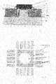
- Figure 1 shows a schematic side view of an electronic component 1 which may, for example, be a discrete LQFP64 (Leadless Quad Flat Pack 64) semiconductor component.
- the electronic component 1 is surface mounted on an upper surface of a printed circuit board 5 which is shown in cross-section in Fig. 1 .
- the component 1 is shown in Fig. 1 having electrical connectors 2, 3 in the shape of pins which project on opposed sides from a casing of the component 1.
- Each of the pins is bent to lie against a respective contact pad 4 which is comprised by the printed circuit board (PCB) 5 and arranged on the upper surface thereof.
- PCB printed circuit board
- the lower surface of the component 1 includes a thermal pad 7.
- the thermal pad 7 is in particular a surface of a metal post which extends from the vicinity of a semiconductor die of the component 1 to a peripheral surface of the component casing.
- the metal post is in particular separate from bonding wires which may electrically connect the semiconductor die to the electrical connectors 2, 3.
- the PCB 5 is provided with an opening 6, the extent of which corresponds to a substantial part of the horizontal extent of the casing of component 1 intermediate to the edges thereof.
- the opening 6 extends through the PCB 5 from its upper surface to a lower surface of the PCB 5 opposite of the upper surface.
- the lower surface of the component 1 - in particular an edge region of the thermal pad 7 - rests on a land 11 for the thermal pad 7 which is comprised by the PCB 5 at its upper surface.
- the land 11 extends circumferentially around the opening 6.
- Thermal vias 8 extend from the land 11 for the thermal pad 7 through the printed circuit board 5 to the lower surface of the printed circuit board, remote from the surface on which the component 1 is mounted.
- the thermal vias 8 and the opening 6 have parallel central axes in this and other embodiments.
- the vias 8 are arranged in annular fashion around the opening 6 in top view of the upper surface of the PCB 5.
- the mounting assembly further comprises a heatsink 10, also shown in cross-section in Fig. 1 .
- the heatsink 10 has a base body which is positioned adjacent to the lower surface of the PCB 5 and follows the lower surface in direction away from the upper surface of the PCB 5.
- An upper surface of the base body faces towards the lower surface of the PCB 5.
- a heatsink extension 10a is formed integrally and in one piece with the base body.
- the heatsink extension 10a extends from the upper surface of the base body into the opening 6 of the PCB 5 and preferably to the upper surface of the PCB 5.
- a free end of the heatsink extension 10a is coplanar with the upper surface of the PCB 5.
- the thermal pad 7 of the component 1 overlaps the heatsink extension 10a in top view of the upper surface of the PCB 5.
- An electrically insulating thermal interface material 9 is provided at the interface between the base body of the heatsink 10 and the PCB 5 and at the interface between the heatsink extension 10a and the thermal pad 7 of the component 1.
- the heatsink extension 10a extends through the opening 6 in the PCB 5 to make an electrically insulating thermal connection with the thermal interface material 9 in the region of the component casing 1 and the thermal pad 7.
- the heatsink extension 10a through the PCB 5 has a truncated conical form such that there is some space between the surface of the heatsink extension 10a and the PCB material representing a peripheral wall of the opening 6.
- the truncated conical extension 10a of the heatsink 10 has a trapezoidal cross-section.
- the heatsink extension 10a is dimensioned and positioned to establish a lateral gap between the surface of the heatsink material and the PCB material which is partly or completely filled with the thermal interface material 9 and to permit some differential thermal expansion between the heatsink extension 10a and the PCB 5.
- thermal interface materials are commercially available and are usually composite materials with particulate fillers to increase the thermal conductivity.
- the heatsink can be made out of cast aluminium or from sheet metal aluminium.
- Figure 2 shows a schematic of a footprint of the land 11 for the thermal pad 7 and of the contact pads 4.
- the land 11 for the thermal pad 7 has a substantially square outline with a centrally located generally circular aperture, such that it extends completely circumferentially around the opening 6.
- the opening 6 enables the heatsink 10 to extend through the PCB 5 to the region of the component casing.
- Three thermal vias 8 are located in each corner of the land 11 for the thermal pad 7 and are arranged as the vertices of a right angle triangle, the apex of which is adjacent to the corner of the thermal pad 7.
- Five contact pads 4 are arranged substantially perpendicularly to the respective edges of the square outline of the land for the thermal pad 7.
- the thermal pad 7 is coupled to the circuit board by a solder connection between the peripheral region of the thermal pad 7 and the land 11 arranged on the upper surface of the circuit board 5 and to the heat sink extension 10a by means of the portion of the thermal interface material 9 arranged in the central portion of the thermal pad 7.
- the extension 10a of the heatsink 10 through the PCB 5 enables the heatsink 10 to make direct thermal contact with the component 1 while remaining electrically insulated from the component 1 and the circuit board 5.
- the component thermal pad 7 is soldered onto the PCB 5 to assure a good electrical connection and also a good mechanical connection.
- the thermal interface material 9 ensures that the thermal pad 7 is electrical insulated from the heatsink 10 whilst at the same time ensuring that there is a low thermal resistance between the thermal pad 7 and the heatsink 10. In high current applications, a good electrical connection is required between the copper ground plane and the plastic ball grid array.
- a thermal simulation was performed using a standard LQFP64 component 1, which comprises 28 thermal vias through a 1.6mm PCB with 0.3mm of thermal interface material between the PCB 5 and the heatsink 10.
- a modified sample was manufactured using the same thermal interface material 9 and thickness of PCB 5 with a circular hole cut in the PCB material as an opening 6 to receive a dome or truncated cone of aluminium heatsink material as heatsink extension 10a.
- Applying a continuous power of 1W to each chip at an ambient temperature of 20 °C produced the results in the table below: Standard Modified R ⁇ junction-ambient 3.48K/W 1.11K/W Max junction temperature 26 °C 24.1 °C
- the modified assembly shows a reduction in the thermal resistance between the component 1 and the heatsink 10 of approximately 70% and a reduction in the maximum junction temperature of around 8-10%.
- the semiconductor electronic component 1 is described as a leadless Quad Flat Pack discrete package, the invention is applicable in other applications where cooling is required such as TO 252 and TO 263 type packages and in cooling high power LEDs, for example.
- the heatsink extension 10a passing through the PCB 5 has been described as having the form of a truncated cone, other shapes would be possible depending on shapes of the thermal pad 7 or electronic component 1.
- the thermal interface material 9 may be arranged between an upper surface of the heat sink extension 10a and the thermal pad 7 and may further be arranged between the base body of the heat sink 10 and the lower surface of the circuit board 5.
Landscapes
- Engineering & Computer Science (AREA)
- Microelectronics & Electronic Packaging (AREA)
- Physics & Mathematics (AREA)
- Thermal Sciences (AREA)
- Cooling Or The Like Of Electrical Apparatus (AREA)
- Cooling Or The Like Of Semiconductors Or Solid State Devices (AREA)
Claims (7)
- Montageanordnung, eine elektronische Komponente (1) umfassend, die auf eine Oberseite einer Leiterplatte (5) montiert ist, wobei die elektronische Komponente (1) mindestens ein elektrisches Verbindungsstück (2, 3) und ein Wärmeleitpad (7) umfasst, wobei- das elektrische Verbindungsstück (2, 3) elektrisch mit einem Kontaktpad (4) der Leiterplatte (5) verbunden ist,- die Leiterplatte (5) an einen Kühlkörper (10) montiert ist, wobei der Kühlkörper (10) eine Kühlkörpererweiterung (10a) aufweist, die sich räumlich von der Leiterplatte (5) getrennt durch selbige erstreckt,- die Leiterplatte (5) mit einer Öffnung (6) unter dem Wärmeleitpad (7) der Komponente (1) versehen ist und eine Anschlussfläche (11) für das Wärmeleitpad (7) umfasst, die sich seitlich rings um die Öffnung (6) erstreckt,- ein Material (9) für eine thermische Grenzfläche bereitgestellt ist,dadurch gekennzeichnet, dass:- die Kühlkörpererweiterung (10a) dafür bemessen und positioniert ist, zwischen der Oberfläche des Kühlkörpermaterials und dem Leiterplattenmaterial einen seitlichen Spalt herzustellen, wobei der Spalt teilweise oder vollständig mit dem Material (9) für eine thermische Grenzfläche gefüllt ist,- das Wärmeleitpad (7) an einer Unterseite der Komponente (1) bereitgestellt und an die Anschlussfläche (11) für das Wärmeleitpad (7) gelötet ist,- das Material (9) für eine thermische Grenzfläche elektrisch isolierend ist und zwischen einer Oberseite der Kühlkörpererweiterung (10a) und dem Wärmeleitpad (7) angeordnet sowie dafür bereitgestellt ist, eine elektrisch isolierende thermische Verbindung zwischen dem Wärmeleitpad (7) und der Kühlkörpererweiterung (10a) sicherzustellen.
- Montageanordnung nach dem vorhergehenden Anspruch, wobei das Material (9) für eine thermische Grenzfläche an das Wärmeleitpad (7) und die Kühlkörpererweiterung (10a) grenzt.
- Montageanordnung nach einem der vorhergehenden Ansprüche, wobei die Kühlkörpererweiterung (10a) die Form eines Kegelstumpfes oder eines Pyramidenstumpfes aufweist.
- Montageanordnung nach einem der vorhergehenden Ansprüche, ferner mehrere thermische Durchkontaktierungen (8) umfassend, die sich von dem Wärmeleitpad (7) durch das Leiterplattenmaterial zu dem Kühlkörper (10) erstrecken.
- Montageanordnung nach einem der vorhergehenden Ansprüche, wobei das Material (9) für eine thermische Grenzfläche ferner zwischen Seitenflächen der Kühlkörpererweiterung und der Öffnung (6) in der Leiterplatte (5) angeordnet ist.
- Montageanordnung nach einem der vorhergehenden Ansprüche, wobei das Material (9) für eine thermische Grenzfläche ferner zwischen dem Kühlkörper (10) und einer Unterseite der Leiterplatte (5) angeordnet ist.
- Montageanordnung nach einem der vorhergehenden Ansprüche, wobei das elektrische Verbindungsstück (2, 3) an das Kontaktpad (4) gelötet ist.
Priority Applications (4)
| Application Number | Priority Date | Filing Date | Title |
|---|---|---|---|
| EP16465550.8A EP3310140B1 (de) | 2016-10-14 | 2016-10-14 | Montageanordnung mit einem kühlkörper |
| PCT/EP2017/076131 WO2018069476A1 (en) | 2016-10-14 | 2017-10-12 | Mounting assembly with a heatsink |
| CN201780063421.0A CN109937617B (zh) | 2016-10-14 | 2017-10-12 | 具有散热片的安装组件 |
| US16/341,997 US10681801B2 (en) | 2016-10-14 | 2017-10-12 | Mounting assembly with a heatsink |
Applications Claiming Priority (1)
| Application Number | Priority Date | Filing Date | Title |
|---|---|---|---|
| EP16465550.8A EP3310140B1 (de) | 2016-10-14 | 2016-10-14 | Montageanordnung mit einem kühlkörper |
Publications (2)
| Publication Number | Publication Date |
|---|---|
| EP3310140A1 EP3310140A1 (de) | 2018-04-18 |
| EP3310140B1 true EP3310140B1 (de) | 2021-07-14 |
Family
ID=57233372
Family Applications (1)
| Application Number | Title | Priority Date | Filing Date |
|---|---|---|---|
| EP16465550.8A Active EP3310140B1 (de) | 2016-10-14 | 2016-10-14 | Montageanordnung mit einem kühlkörper |
Country Status (4)
| Country | Link |
|---|---|
| US (1) | US10681801B2 (de) |
| EP (1) | EP3310140B1 (de) |
| CN (1) | CN109937617B (de) |
| WO (1) | WO2018069476A1 (de) |
Families Citing this family (15)
| Publication number | Priority date | Publication date | Assignee | Title |
|---|---|---|---|---|
| IL326076A (en) | 2016-06-06 | 2026-03-01 | Sofwave Medical Ltd | Ultrasound system and transducer |
| EP3829713B1 (de) | 2018-08-02 | 2025-10-01 | Sofwave Medical Ltd. | System zur behandlung von fettgewebe |
| DE102019107080B4 (de) * | 2019-03-20 | 2021-08-12 | Semikron Elektronik Gmbh & Co. Kg | Anordnung mit einer Leiterplatte und einem zu entwärmenden Leistungshalbleiterbauelement |
| CN115053346A (zh) * | 2019-12-06 | 2022-09-13 | 生物辐射实验室股份有限公司 | 用于图像传感器的具有导热结构的电子部件组件 |
| US11416045B2 (en) | 2020-04-13 | 2022-08-16 | International Business Machines Corporation | Thermal interface material structures for directing heat in a three-dimensional space |
| WO2022004281A1 (ja) * | 2020-07-02 | 2022-01-06 | 株式会社村田製作所 | 多層回路基板および電子部品実装多層基板 |
| CN114630547A (zh) * | 2020-12-10 | 2022-06-14 | 中兴通讯股份有限公司 | 散热装置及电子设备 |
| JP7447785B2 (ja) * | 2020-12-25 | 2024-03-12 | 株式会社デンソー | 電子装置 |
| CA3203037A1 (en) * | 2020-12-31 | 2022-07-07 | Ariel Sverdlik | Cooling of ultrasound energizers mounted on printed circuit boards |
| JP7495902B2 (ja) * | 2021-04-01 | 2024-06-05 | 日本特殊陶業株式会社 | 半導体パッケージ |
| US11910518B2 (en) * | 2021-05-26 | 2024-02-20 | Huawei Technologies Canada Co., Ltd. | Method and apparatus for heat sink mounting |
| TWI787877B (zh) * | 2021-06-22 | 2022-12-21 | 啟碁科技股份有限公司 | 散熱結構 |
| US11910573B2 (en) * | 2021-10-25 | 2024-02-20 | Mellanox Technologies Ltd. | Mechanical device for cooling an electronic component |
| EP4633306A1 (de) * | 2024-04-11 | 2025-10-15 | Aptiv Technologies AG | Elektronische vorrichtung für kraftfahrzeuge |
| WO2026013098A1 (en) * | 2024-07-11 | 2026-01-15 | Signify Holding B.V. | Method of cooling high power pcb mounted components |
Family Cites Families (20)
| Publication number | Priority date | Publication date | Assignee | Title |
|---|---|---|---|---|
| GB8304890D0 (en) * | 1983-02-22 | 1983-03-23 | Smiths Industries Plc | Chip-carrier substrates |
| US4941067A (en) | 1989-04-07 | 1990-07-10 | Motorola Inc. | Thermal shunt for electronic circuits |
| US5172755A (en) | 1992-04-01 | 1992-12-22 | Digital Equipment Corporation | Arcuate profiled heatsink apparatus and method |
| DE19601649A1 (de) * | 1996-01-18 | 1997-07-24 | Telefunken Microelectron | Anordnung zur Verbesserung der Wärmeableitung bei elektrischen und elektronischen Bauelementen |
| JPH09213877A (ja) | 1996-02-02 | 1997-08-15 | Toshiba Corp | マルチチップモジュール半導体装置 |
| US5920458A (en) | 1997-05-28 | 1999-07-06 | Lucent Technologies Inc. | Enhanced cooling of a heat dissipating circuit element |
| US7061080B2 (en) | 2001-06-11 | 2006-06-13 | Fairchild Korea Semiconductor Ltd. | Power module package having improved heat dissipating capability |
| SE529673C2 (sv) | 2004-09-20 | 2007-10-16 | Danaher Motion Stockholm Ab | Kretsarrangemang för kylning av ytmonterade halvledare |
| US7457126B2 (en) | 2005-06-27 | 2008-11-25 | Intel Corporation | Optical transponder with active heat transfer |
| TW200836044A (en) | 2007-02-16 | 2008-09-01 | Delta Electronics Thailand Public Co Ltd | Heat-dissipating module |
| US20100072511A1 (en) * | 2008-03-25 | 2010-03-25 | Lin Charles W C | Semiconductor chip assembly with copper/aluminum post/base heat spreader |
| GB2460124A (en) * | 2008-05-21 | 2009-11-25 | Nujira Ltd | Printed circuit board with co-planar plate |
| GB2461548B (en) * | 2008-07-02 | 2010-10-13 | Thales Holdings Uk Plc | Printed circuit board assembly |
| US20110272179A1 (en) | 2010-05-06 | 2011-11-10 | Vasoya Kalu K | Printed Circuit Board with Embossed Hollow Heatsink Pad |
| US8354684B2 (en) | 2011-01-09 | 2013-01-15 | Bridgelux, Inc. | Packaging photon building blocks having only top side connections in an interconnect structure |
| US9209163B2 (en) | 2011-08-19 | 2015-12-08 | Marvell World Trade Ltd. | Package-on-package structures |
| US8929077B2 (en) | 2012-01-02 | 2015-01-06 | Tem Products Inc. | Thermal connector |
| WO2014158388A1 (en) * | 2013-02-11 | 2014-10-02 | Marvell World Trade Ltd. | Package-on-package structures |
| CN103438409A (zh) | 2013-07-30 | 2013-12-11 | 福建永德吉灯业股份有限公司 | 一种led的铝散热模块 |
| US9668334B2 (en) * | 2014-05-23 | 2017-05-30 | General Electric Company | Thermal clamp apparatus for electronic systems |
-
2016
- 2016-10-14 EP EP16465550.8A patent/EP3310140B1/de active Active
-
2017
- 2017-10-12 WO PCT/EP2017/076131 patent/WO2018069476A1/en not_active Ceased
- 2017-10-12 US US16/341,997 patent/US10681801B2/en active Active
- 2017-10-12 CN CN201780063421.0A patent/CN109937617B/zh active Active
Non-Patent Citations (1)
| Title |
|---|
| None * |
Also Published As
| Publication number | Publication date |
|---|---|
| US10681801B2 (en) | 2020-06-09 |
| EP3310140A1 (de) | 2018-04-18 |
| CN109937617B (zh) | 2020-12-01 |
| WO2018069476A1 (en) | 2018-04-19 |
| CN109937617A (zh) | 2019-06-25 |
| US20190254157A1 (en) | 2019-08-15 |
Similar Documents
| Publication | Publication Date | Title |
|---|---|---|
| EP3310140B1 (de) | Montageanordnung mit einem kühlkörper | |
| US9107290B1 (en) | Package structure and stacked package module with the same | |
| US9425131B2 (en) | Package structure | |
| TWI587759B (zh) | 三維空間封裝結構及其製造方法 | |
| US8159828B2 (en) | Low profile flip chip power module and method of making | |
| KR100458832B1 (ko) | 리드리스 칩 캐리어의 설계 및 구조 | |
| JP6891274B2 (ja) | 電子機器 | |
| US8916958B2 (en) | Semiconductor package with multiple chips and substrate in metal cap | |
| US9271388B2 (en) | Interposer and package on package structure | |
| US11749589B2 (en) | Module | |
| US20240114614A1 (en) | Thermal Conduction - Electrical Conduction Isolated Circuit Board with Ceramic Substrate and Power Transistor Embedded | |
| CN101322450B (zh) | 具有内部散热结构的ic封装 | |
| CN111031687A (zh) | 制备散热电路板的方法 | |
| EP2058860A2 (de) | Zur zweiseitigen Kühlung konfiguriertes, vollständig prüfbares, oberflächenmontiertes Formgehäuse | |
| US7310224B2 (en) | Electronic apparatus with thermal module | |
| JP2020202329A (ja) | 電子制御装置 | |
| KR20060105403A (ko) | 혼성회로와 복합기판을 가지는 패키지 구조물 | |
| JP4810235B2 (ja) | 半導体装置とそれを用いた電子部品モジュール | |
| JP4919689B2 (ja) | モジュール基板 | |
| US11798873B2 (en) | Semiconductor assembly | |
| CN223899713U (zh) | 定向散热的功率芯片封装模块 | |
| CN114496808B (zh) | 倒装式塑封的装配方法、屏蔽系统、散热系统及应用 | |
| JP2005183879A (ja) | 高放熱型プラスチックパッケージ | |
| KR19990071282A (ko) | 반도체 패키지 제조방법 | |
| JP2016171202A (ja) | 電子装置 |
Legal Events
| Date | Code | Title | Description |
|---|---|---|---|
| PUAI | Public reference made under article 153(3) epc to a published international application that has entered the european phase |
Free format text: ORIGINAL CODE: 0009012 |
|
| STAA | Information on the status of an ep patent application or granted ep patent |
Free format text: STATUS: THE APPLICATION HAS BEEN PUBLISHED |
|
| AK | Designated contracting states |
Kind code of ref document: A1 Designated state(s): AL AT BE BG CH CY CZ DE DK EE ES FI FR GB GR HR HU IE IS IT LI LT LU LV MC MK MT NL NO PL PT RO RS SE SI SK SM TR |
|
| AX | Request for extension of the european patent |
Extension state: BA ME |
|
| STAA | Information on the status of an ep patent application or granted ep patent |
Free format text: STATUS: REQUEST FOR EXAMINATION WAS MADE |
|
| 17P | Request for examination filed |
Effective date: 20181018 |
|
| RBV | Designated contracting states (corrected) |
Designated state(s): AL AT BE BG CH CY CZ DE DK EE ES FI FR GB GR HR HU IE IS IT LI LT LU LV MC MK MT NL NO PL PT RO RS SE SI SK SM TR |
|
| RAP1 | Party data changed (applicant data changed or rights of an application transferred) |
Owner name: VITESCO TECHNOLOGIES GMBH |
|
| STAA | Information on the status of an ep patent application or granted ep patent |
Free format text: STATUS: EXAMINATION IS IN PROGRESS |
|
| 17Q | First examination report despatched |
Effective date: 20200921 |
|
| GRAP | Despatch of communication of intention to grant a patent |
Free format text: ORIGINAL CODE: EPIDOSNIGR1 |
|
| STAA | Information on the status of an ep patent application or granted ep patent |
Free format text: STATUS: GRANT OF PATENT IS INTENDED |
|
| INTG | Intention to grant announced |
Effective date: 20210312 |
|
| GRAS | Grant fee paid |
Free format text: ORIGINAL CODE: EPIDOSNIGR3 |
|
| GRAA | (expected) grant |
Free format text: ORIGINAL CODE: 0009210 |
|
| STAA | Information on the status of an ep patent application or granted ep patent |
Free format text: STATUS: THE PATENT HAS BEEN GRANTED |
|
| AK | Designated contracting states |
Kind code of ref document: B1 Designated state(s): AL AT BE BG CH CY CZ DE DK EE ES FI FR GB GR HR HU IE IS IT LI LT LU LV MC MK MT NL NO PL PT RO RS SE SI SK SM TR |
|
| REG | Reference to a national code |
Ref country code: GB Ref legal event code: FG4D |
|
| REG | Reference to a national code |
Ref country code: DE Ref legal event code: R096 Ref document number: 602016060567 Country of ref document: DE |
|
| REG | Reference to a national code |
Ref country code: IE Ref legal event code: FG4D |
|
| REG | Reference to a national code |
Ref country code: AT Ref legal event code: REF Ref document number: 1411703 Country of ref document: AT Kind code of ref document: T Effective date: 20210815 |
|
| REG | Reference to a national code |
Ref country code: LT Ref legal event code: MG9D |
|
| REG | Reference to a national code |
Ref country code: NL Ref legal event code: MP Effective date: 20210714 |
|
| RAP4 | Party data changed (patent owner data changed or rights of a patent transferred) |
Owner name: VITESCO TECHNOLOGIES GMBH |
|
| REG | Reference to a national code |
Ref country code: AT Ref legal event code: MK05 Ref document number: 1411703 Country of ref document: AT Kind code of ref document: T Effective date: 20210714 |
|
| REG | Reference to a national code |
Ref country code: DE Ref legal event code: R081 Ref document number: 602016060567 Country of ref document: DE Owner name: SCHAEFFLER TECHNOLOGIES AG & CO. KG, DE Free format text: FORMER OWNER: VITESCO TECHNOLOGIES GMBH, 30165 HANNOVER, DE Ref country code: DE Ref legal event code: R081 Ref document number: 602016060567 Country of ref document: DE Owner name: VITESCO TECHNOLOGIES GMBH, DE Free format text: FORMER OWNER: VITESCO TECHNOLOGIES GMBH, 30165 HANNOVER, DE |
|
| PG25 | Lapsed in a contracting state [announced via postgrant information from national office to epo] |
Ref country code: SE Free format text: LAPSE BECAUSE OF FAILURE TO SUBMIT A TRANSLATION OF THE DESCRIPTION OR TO PAY THE FEE WITHIN THE PRESCRIBED TIME-LIMIT Effective date: 20210714 Ref country code: RS Free format text: LAPSE BECAUSE OF FAILURE TO SUBMIT A TRANSLATION OF THE DESCRIPTION OR TO PAY THE FEE WITHIN THE PRESCRIBED TIME-LIMIT Effective date: 20210714 Ref country code: PT Free format text: LAPSE BECAUSE OF FAILURE TO SUBMIT A TRANSLATION OF THE DESCRIPTION OR TO PAY THE FEE WITHIN THE PRESCRIBED TIME-LIMIT Effective date: 20211115 Ref country code: NL Free format text: LAPSE BECAUSE OF FAILURE TO SUBMIT A TRANSLATION OF THE DESCRIPTION OR TO PAY THE FEE WITHIN THE PRESCRIBED TIME-LIMIT Effective date: 20210714 Ref country code: NO Free format text: LAPSE BECAUSE OF FAILURE TO SUBMIT A TRANSLATION OF THE DESCRIPTION OR TO PAY THE FEE WITHIN THE PRESCRIBED TIME-LIMIT Effective date: 20211014 Ref country code: HR Free format text: LAPSE BECAUSE OF FAILURE TO SUBMIT A TRANSLATION OF THE DESCRIPTION OR TO PAY THE FEE WITHIN THE PRESCRIBED TIME-LIMIT Effective date: 20210714 Ref country code: FI Free format text: LAPSE BECAUSE OF FAILURE TO SUBMIT A TRANSLATION OF THE DESCRIPTION OR TO PAY THE FEE WITHIN THE PRESCRIBED TIME-LIMIT Effective date: 20210714 Ref country code: ES Free format text: LAPSE BECAUSE OF FAILURE TO SUBMIT A TRANSLATION OF THE DESCRIPTION OR TO PAY THE FEE WITHIN THE PRESCRIBED TIME-LIMIT Effective date: 20210714 Ref country code: LT Free format text: LAPSE BECAUSE OF FAILURE TO SUBMIT A TRANSLATION OF THE DESCRIPTION OR TO PAY THE FEE WITHIN THE PRESCRIBED TIME-LIMIT Effective date: 20210714 Ref country code: AT Free format text: LAPSE BECAUSE OF FAILURE TO SUBMIT A TRANSLATION OF THE DESCRIPTION OR TO PAY THE FEE WITHIN THE PRESCRIBED TIME-LIMIT Effective date: 20210714 Ref country code: BG Free format text: LAPSE BECAUSE OF FAILURE TO SUBMIT A TRANSLATION OF THE DESCRIPTION OR TO PAY THE FEE WITHIN THE PRESCRIBED TIME-LIMIT Effective date: 20211014 |
|
| PG25 | Lapsed in a contracting state [announced via postgrant information from national office to epo] |
Ref country code: PL Free format text: LAPSE BECAUSE OF FAILURE TO SUBMIT A TRANSLATION OF THE DESCRIPTION OR TO PAY THE FEE WITHIN THE PRESCRIBED TIME-LIMIT Effective date: 20210714 Ref country code: LV Free format text: LAPSE BECAUSE OF FAILURE TO SUBMIT A TRANSLATION OF THE DESCRIPTION OR TO PAY THE FEE WITHIN THE PRESCRIBED TIME-LIMIT Effective date: 20210714 Ref country code: GR Free format text: LAPSE BECAUSE OF FAILURE TO SUBMIT A TRANSLATION OF THE DESCRIPTION OR TO PAY THE FEE WITHIN THE PRESCRIBED TIME-LIMIT Effective date: 20211015 |
|
| REG | Reference to a national code |
Ref country code: DE Ref legal event code: R097 Ref document number: 602016060567 Country of ref document: DE |
|
| PG25 | Lapsed in a contracting state [announced via postgrant information from national office to epo] |
Ref country code: DK Free format text: LAPSE BECAUSE OF FAILURE TO SUBMIT A TRANSLATION OF THE DESCRIPTION OR TO PAY THE FEE WITHIN THE PRESCRIBED TIME-LIMIT Effective date: 20210714 |
|
| PLBE | No opposition filed within time limit |
Free format text: ORIGINAL CODE: 0009261 |
|
| STAA | Information on the status of an ep patent application or granted ep patent |
Free format text: STATUS: NO OPPOSITION FILED WITHIN TIME LIMIT |
|
| REG | Reference to a national code |
Ref country code: CH Ref legal event code: PL |
|
| PG25 | Lapsed in a contracting state [announced via postgrant information from national office to epo] |
Ref country code: SM Free format text: LAPSE BECAUSE OF FAILURE TO SUBMIT A TRANSLATION OF THE DESCRIPTION OR TO PAY THE FEE WITHIN THE PRESCRIBED TIME-LIMIT Effective date: 20210714 Ref country code: SK Free format text: LAPSE BECAUSE OF FAILURE TO SUBMIT A TRANSLATION OF THE DESCRIPTION OR TO PAY THE FEE WITHIN THE PRESCRIBED TIME-LIMIT Effective date: 20210714 Ref country code: RO Free format text: LAPSE BECAUSE OF FAILURE TO SUBMIT A TRANSLATION OF THE DESCRIPTION OR TO PAY THE FEE WITHIN THE PRESCRIBED TIME-LIMIT Effective date: 20210714 Ref country code: EE Free format text: LAPSE BECAUSE OF FAILURE TO SUBMIT A TRANSLATION OF THE DESCRIPTION OR TO PAY THE FEE WITHIN THE PRESCRIBED TIME-LIMIT Effective date: 20210714 Ref country code: CZ Free format text: LAPSE BECAUSE OF FAILURE TO SUBMIT A TRANSLATION OF THE DESCRIPTION OR TO PAY THE FEE WITHIN THE PRESCRIBED TIME-LIMIT Effective date: 20210714 Ref country code: AL Free format text: LAPSE BECAUSE OF FAILURE TO SUBMIT A TRANSLATION OF THE DESCRIPTION OR TO PAY THE FEE WITHIN THE PRESCRIBED TIME-LIMIT Effective date: 20210714 |
|
| 26N | No opposition filed |
Effective date: 20220419 |
|
| REG | Reference to a national code |
Ref country code: BE Ref legal event code: MM Effective date: 20211031 |
|
| GBPC | Gb: european patent ceased through non-payment of renewal fee |
Effective date: 20211014 |
|
| PG25 | Lapsed in a contracting state [announced via postgrant information from national office to epo] |
Ref country code: MC Free format text: LAPSE BECAUSE OF FAILURE TO SUBMIT A TRANSLATION OF THE DESCRIPTION OR TO PAY THE FEE WITHIN THE PRESCRIBED TIME-LIMIT Effective date: 20210714 |
|
| PG25 | Lapsed in a contracting state [announced via postgrant information from national office to epo] |
Ref country code: LU Free format text: LAPSE BECAUSE OF NON-PAYMENT OF DUE FEES Effective date: 20211014 Ref country code: IT Free format text: LAPSE BECAUSE OF FAILURE TO SUBMIT A TRANSLATION OF THE DESCRIPTION OR TO PAY THE FEE WITHIN THE PRESCRIBED TIME-LIMIT Effective date: 20210714 Ref country code: GB Free format text: LAPSE BECAUSE OF NON-PAYMENT OF DUE FEES Effective date: 20211014 Ref country code: BE Free format text: LAPSE BECAUSE OF NON-PAYMENT OF DUE FEES Effective date: 20211031 |
|
| PG25 | Lapsed in a contracting state [announced via postgrant information from national office to epo] |
Ref country code: LI Free format text: LAPSE BECAUSE OF NON-PAYMENT OF DUE FEES Effective date: 20211031 Ref country code: CH Free format text: LAPSE BECAUSE OF NON-PAYMENT OF DUE FEES Effective date: 20211031 |
|
| PG25 | Lapsed in a contracting state [announced via postgrant information from national office to epo] |
Ref country code: FR Free format text: LAPSE BECAUSE OF NON-PAYMENT OF DUE FEES Effective date: 20211031 |
|
| PG25 | Lapsed in a contracting state [announced via postgrant information from national office to epo] |
Ref country code: IE Free format text: LAPSE BECAUSE OF NON-PAYMENT OF DUE FEES Effective date: 20211014 |
|
| PG25 | Lapsed in a contracting state [announced via postgrant information from national office to epo] |
Ref country code: HU Free format text: LAPSE BECAUSE OF FAILURE TO SUBMIT A TRANSLATION OF THE DESCRIPTION OR TO PAY THE FEE WITHIN THE PRESCRIBED TIME-LIMIT; INVALID AB INITIO Effective date: 20161014 |
|
| PG25 | Lapsed in a contracting state [announced via postgrant information from national office to epo] |
Ref country code: CY Free format text: LAPSE BECAUSE OF FAILURE TO SUBMIT A TRANSLATION OF THE DESCRIPTION OR TO PAY THE FEE WITHIN THE PRESCRIBED TIME-LIMIT Effective date: 20210714 |
|
| P01 | Opt-out of the competence of the unified patent court (upc) registered |
Effective date: 20230530 |
|
| PG25 | Lapsed in a contracting state [announced via postgrant information from national office to epo] |
Ref country code: MK Free format text: LAPSE BECAUSE OF FAILURE TO SUBMIT A TRANSLATION OF THE DESCRIPTION OR TO PAY THE FEE WITHIN THE PRESCRIBED TIME-LIMIT Effective date: 20210714 |
|
| PG25 | Lapsed in a contracting state [announced via postgrant information from national office to epo] |
Ref country code: MT Free format text: LAPSE BECAUSE OF FAILURE TO SUBMIT A TRANSLATION OF THE DESCRIPTION OR TO PAY THE FEE WITHIN THE PRESCRIBED TIME-LIMIT Effective date: 20210714 |
|
| REG | Reference to a national code |
Ref country code: DE Ref legal event code: R081 Ref document number: 602016060567 Country of ref document: DE Owner name: SCHAEFFLER TECHNOLOGIES AG & CO. KG, DE Free format text: FORMER OWNER: VITESCO TECHNOLOGIES GMBH, 93055 REGENSBURG, DE |
|
| PG25 | Lapsed in a contracting state [announced via postgrant information from national office to epo] |
Ref country code: TR Free format text: LAPSE BECAUSE OF FAILURE TO SUBMIT A TRANSLATION OF THE DESCRIPTION OR TO PAY THE FEE WITHIN THE PRESCRIBED TIME-LIMIT Effective date: 20210714 |
|
| PGFP | Annual fee paid to national office [announced via postgrant information from national office to epo] |
Ref country code: DE Payment date: 20251031 Year of fee payment: 10 |