EP3312667B1 - Dispositif d'affichage à cristaux liquides et son procédé de fabrication - Google Patents
Dispositif d'affichage à cristaux liquides et son procédé de fabrication Download PDFInfo
- Publication number
- EP3312667B1 EP3312667B1 EP16811541.8A EP16811541A EP3312667B1 EP 3312667 B1 EP3312667 B1 EP 3312667B1 EP 16811541 A EP16811541 A EP 16811541A EP 3312667 B1 EP3312667 B1 EP 3312667B1
- Authority
- EP
- European Patent Office
- Prior art keywords
- group
- liquid crystal
- carbon atoms
- substrate
- alkyl group
- Prior art date
- Legal status (The legal status is an assumption and is not a legal conclusion. Google has not performed a legal analysis and makes no representation as to the accuracy of the status listed.)
- Active
Links
- 0 CC1C(CC(CC2)CC(C3)C3C2C2C=**CC2)C1 Chemical compound CC1C(CC(CC2)CC(C3)C3C2C2C=**CC2)C1 0.000 description 14
- RPMUDXVQHUECRE-UHFFFAOYSA-N CC1COC(C)OC1 Chemical compound CC1COC(C)OC1 RPMUDXVQHUECRE-UHFFFAOYSA-N 0.000 description 2
- JMPQQXWPKDTARU-UHFFFAOYSA-N CC1C2CCC1C2 Chemical compound CC1C2CCC1C2 JMPQQXWPKDTARU-UHFFFAOYSA-N 0.000 description 1
Images


Classifications
-
- C—CHEMISTRY; METALLURGY
- C09—DYES; PAINTS; POLISHES; NATURAL RESINS; ADHESIVES; COMPOSITIONS NOT OTHERWISE PROVIDED FOR; APPLICATIONS OF MATERIALS NOT OTHERWISE PROVIDED FOR
- C09K—MATERIALS FOR MISCELLANEOUS APPLICATIONS, NOT PROVIDED FOR ELSEWHERE
- C09K19/00—Liquid crystal materials
- C09K19/04—Liquid crystal materials characterised by the chemical structure of the liquid crystal components, e.g. by a specific unit
- C09K19/06—Non-steroidal liquid crystal compounds
- C09K19/08—Non-steroidal liquid crystal compounds containing at least two non-condensed rings
- C09K19/30—Non-steroidal liquid crystal compounds containing at least two non-condensed rings containing saturated or unsaturated non-aromatic rings, e.g. cyclohexane rings
-
- C—CHEMISTRY; METALLURGY
- C09—DYES; PAINTS; POLISHES; NATURAL RESINS; ADHESIVES; COMPOSITIONS NOT OTHERWISE PROVIDED FOR; APPLICATIONS OF MATERIALS NOT OTHERWISE PROVIDED FOR
- C09K—MATERIALS FOR MISCELLANEOUS APPLICATIONS, NOT PROVIDED FOR ELSEWHERE
- C09K19/00—Liquid crystal materials
- C09K19/52—Liquid crystal materials characterised by components which are not liquid crystals, e.g. additives with special physical aspect: solvents, solid particles
- C09K19/54—Additives having no specific mesophase characterised by their chemical composition
- C09K19/56—Aligning agents
-
- C—CHEMISTRY; METALLURGY
- C09—DYES; PAINTS; POLISHES; NATURAL RESINS; ADHESIVES; COMPOSITIONS NOT OTHERWISE PROVIDED FOR; APPLICATIONS OF MATERIALS NOT OTHERWISE PROVIDED FOR
- C09K—MATERIALS FOR MISCELLANEOUS APPLICATIONS, NOT PROVIDED FOR ELSEWHERE
- C09K19/00—Liquid crystal materials
- C09K19/52—Liquid crystal materials characterised by components which are not liquid crystals, e.g. additives with special physical aspect: solvents, solid particles
- C09K19/54—Additives having no specific mesophase characterised by their chemical composition
- C09K19/542—Macromolecular compounds
-
- C—CHEMISTRY; METALLURGY
- C09—DYES; PAINTS; POLISHES; NATURAL RESINS; ADHESIVES; COMPOSITIONS NOT OTHERWISE PROVIDED FOR; APPLICATIONS OF MATERIALS NOT OTHERWISE PROVIDED FOR
- C09K—MATERIALS FOR MISCELLANEOUS APPLICATIONS, NOT PROVIDED FOR ELSEWHERE
- C09K19/00—Liquid crystal materials
- C09K19/04—Liquid crystal materials characterised by the chemical structure of the liquid crystal components, e.g. by a specific unit
- C09K19/06—Non-steroidal liquid crystal compounds
- C09K19/08—Non-steroidal liquid crystal compounds containing at least two non-condensed rings
- C09K19/30—Non-steroidal liquid crystal compounds containing at least two non-condensed rings containing saturated or unsaturated non-aromatic rings, e.g. cyclohexane rings
- C09K19/3001—Cyclohexane rings
- C09K19/3003—Compounds containing at least two rings in which the different rings are directly linked (covalent bond)
-
- C—CHEMISTRY; METALLURGY
- C09—DYES; PAINTS; POLISHES; NATURAL RESINS; ADHESIVES; COMPOSITIONS NOT OTHERWISE PROVIDED FOR; APPLICATIONS OF MATERIALS NOT OTHERWISE PROVIDED FOR
- C09K—MATERIALS FOR MISCELLANEOUS APPLICATIONS, NOT PROVIDED FOR ELSEWHERE
- C09K19/00—Liquid crystal materials
- C09K19/04—Liquid crystal materials characterised by the chemical structure of the liquid crystal components, e.g. by a specific unit
- C09K19/06—Non-steroidal liquid crystal compounds
- C09K19/08—Non-steroidal liquid crystal compounds containing at least two non-condensed rings
- C09K19/30—Non-steroidal liquid crystal compounds containing at least two non-condensed rings containing saturated or unsaturated non-aromatic rings, e.g. cyclohexane rings
- C09K19/3001—Cyclohexane rings
- C09K19/3066—Cyclohexane rings in which the rings are linked by a chain containing carbon and oxygen atoms, e.g. esters or ethers
-
- C—CHEMISTRY; METALLURGY
- C09—DYES; PAINTS; POLISHES; NATURAL RESINS; ADHESIVES; COMPOSITIONS NOT OTHERWISE PROVIDED FOR; APPLICATIONS OF MATERIALS NOT OTHERWISE PROVIDED FOR
- C09K—MATERIALS FOR MISCELLANEOUS APPLICATIONS, NOT PROVIDED FOR ELSEWHERE
- C09K19/00—Liquid crystal materials
- C09K19/52—Liquid crystal materials characterised by components which are not liquid crystals, e.g. additives with special physical aspect: solvents, solid particles
- C09K19/54—Additives having no specific mesophase characterised by their chemical composition
-
- G—PHYSICS
- G02—OPTICS
- G02F—OPTICAL DEVICES OR ARRANGEMENTS FOR THE CONTROL OF LIGHT BY MODIFICATION OF THE OPTICAL PROPERTIES OF THE MEDIA OF THE ELEMENTS INVOLVED THEREIN; NON-LINEAR OPTICS; FREQUENCY-CHANGING OF LIGHT; OPTICAL LOGIC ELEMENTS; OPTICAL ANALOGUE/DIGITAL CONVERTERS
- G02F1/00—Devices or arrangements for the control of the intensity, colour, phase, polarisation or direction of light arriving from an independent light source, e.g. switching, gating or modulating; Non-linear optics
- G02F1/01—Devices or arrangements for the control of the intensity, colour, phase, polarisation or direction of light arriving from an independent light source, e.g. switching, gating or modulating; Non-linear optics for the control of the intensity, phase, polarisation or colour
- G02F1/13—Devices or arrangements for the control of the intensity, colour, phase, polarisation or direction of light arriving from an independent light source, e.g. switching, gating or modulating; Non-linear optics for the control of the intensity, phase, polarisation or colour based on liquid crystals, e.g. single liquid crystal display cells
-
- G—PHYSICS
- G02—OPTICS
- G02F—OPTICAL DEVICES OR ARRANGEMENTS FOR THE CONTROL OF LIGHT BY MODIFICATION OF THE OPTICAL PROPERTIES OF THE MEDIA OF THE ELEMENTS INVOLVED THEREIN; NON-LINEAR OPTICS; FREQUENCY-CHANGING OF LIGHT; OPTICAL LOGIC ELEMENTS; OPTICAL ANALOGUE/DIGITAL CONVERTERS
- G02F1/00—Devices or arrangements for the control of the intensity, colour, phase, polarisation or direction of light arriving from an independent light source, e.g. switching, gating or modulating; Non-linear optics
- G02F1/01—Devices or arrangements for the control of the intensity, colour, phase, polarisation or direction of light arriving from an independent light source, e.g. switching, gating or modulating; Non-linear optics for the control of the intensity, phase, polarisation or colour
- G02F1/13—Devices or arrangements for the control of the intensity, colour, phase, polarisation or direction of light arriving from an independent light source, e.g. switching, gating or modulating; Non-linear optics for the control of the intensity, phase, polarisation or colour based on liquid crystals, e.g. single liquid crystal display cells
- G02F1/133—Constructional arrangements; Operation of liquid crystal cells; Circuit arrangements
- G02F1/1333—Constructional arrangements; Manufacturing methods
- G02F1/1337—Surface-induced orientation of the liquid crystal molecules, e.g. by alignment layers
-
- G—PHYSICS
- G02—OPTICS
- G02F—OPTICAL DEVICES OR ARRANGEMENTS FOR THE CONTROL OF LIGHT BY MODIFICATION OF THE OPTICAL PROPERTIES OF THE MEDIA OF THE ELEMENTS INVOLVED THEREIN; NON-LINEAR OPTICS; FREQUENCY-CHANGING OF LIGHT; OPTICAL LOGIC ELEMENTS; OPTICAL ANALOGUE/DIGITAL CONVERTERS
- G02F1/00—Devices or arrangements for the control of the intensity, colour, phase, polarisation or direction of light arriving from an independent light source, e.g. switching, gating or modulating; Non-linear optics
- G02F1/01—Devices or arrangements for the control of the intensity, colour, phase, polarisation or direction of light arriving from an independent light source, e.g. switching, gating or modulating; Non-linear optics for the control of the intensity, phase, polarisation or colour
- G02F1/13—Devices or arrangements for the control of the intensity, colour, phase, polarisation or direction of light arriving from an independent light source, e.g. switching, gating or modulating; Non-linear optics for the control of the intensity, phase, polarisation or colour based on liquid crystals, e.g. single liquid crystal display cells
- G02F1/133—Constructional arrangements; Operation of liquid crystal cells; Circuit arrangements
- G02F1/1333—Constructional arrangements; Manufacturing methods
- G02F1/1341—Filling or closing of cells
-
- G—PHYSICS
- G02—OPTICS
- G02F—OPTICAL DEVICES OR ARRANGEMENTS FOR THE CONTROL OF LIGHT BY MODIFICATION OF THE OPTICAL PROPERTIES OF THE MEDIA OF THE ELEMENTS INVOLVED THEREIN; NON-LINEAR OPTICS; FREQUENCY-CHANGING OF LIGHT; OPTICAL LOGIC ELEMENTS; OPTICAL ANALOGUE/DIGITAL CONVERTERS
- G02F1/00—Devices or arrangements for the control of the intensity, colour, phase, polarisation or direction of light arriving from an independent light source, e.g. switching, gating or modulating; Non-linear optics
- G02F1/01—Devices or arrangements for the control of the intensity, colour, phase, polarisation or direction of light arriving from an independent light source, e.g. switching, gating or modulating; Non-linear optics for the control of the intensity, phase, polarisation or colour
- G02F1/13—Devices or arrangements for the control of the intensity, colour, phase, polarisation or direction of light arriving from an independent light source, e.g. switching, gating or modulating; Non-linear optics for the control of the intensity, phase, polarisation or colour based on liquid crystals, e.g. single liquid crystal display cells
- G02F1/133—Constructional arrangements; Operation of liquid crystal cells; Circuit arrangements
- G02F1/136—Liquid crystal cells structurally associated with a semi-conducting layer or substrate, e.g. cells forming part of an integrated circuit
- G02F1/1362—Active matrix addressed cells
- G02F1/1368—Active matrix addressed cells in which the switching element is a three-electrode device
-
- G—PHYSICS
- G02—OPTICS
- G02F—OPTICAL DEVICES OR ARRANGEMENTS FOR THE CONTROL OF LIGHT BY MODIFICATION OF THE OPTICAL PROPERTIES OF THE MEDIA OF THE ELEMENTS INVOLVED THEREIN; NON-LINEAR OPTICS; FREQUENCY-CHANGING OF LIGHT; OPTICAL LOGIC ELEMENTS; OPTICAL ANALOGUE/DIGITAL CONVERTERS
- G02F1/00—Devices or arrangements for the control of the intensity, colour, phase, polarisation or direction of light arriving from an independent light source, e.g. switching, gating or modulating; Non-linear optics
- G02F1/01—Devices or arrangements for the control of the intensity, colour, phase, polarisation or direction of light arriving from an independent light source, e.g. switching, gating or modulating; Non-linear optics for the control of the intensity, phase, polarisation or colour
- G02F1/13—Devices or arrangements for the control of the intensity, colour, phase, polarisation or direction of light arriving from an independent light source, e.g. switching, gating or modulating; Non-linear optics for the control of the intensity, phase, polarisation or colour based on liquid crystals, e.g. single liquid crystal display cells
- G02F1/137—Devices or arrangements for the control of the intensity, colour, phase, polarisation or direction of light arriving from an independent light source, e.g. switching, gating or modulating; Non-linear optics for the control of the intensity, phase, polarisation or colour based on liquid crystals, e.g. single liquid crystal display cells characterised by the electro-optical or magneto-optical effect, e.g. field-induced phase transition, orientation effect, guest-host interaction or dynamic scattering
-
- C—CHEMISTRY; METALLURGY
- C09—DYES; PAINTS; POLISHES; NATURAL RESINS; ADHESIVES; COMPOSITIONS NOT OTHERWISE PROVIDED FOR; APPLICATIONS OF MATERIALS NOT OTHERWISE PROVIDED FOR
- C09K—MATERIALS FOR MISCELLANEOUS APPLICATIONS, NOT PROVIDED FOR ELSEWHERE
- C09K19/00—Liquid crystal materials
- C09K19/04—Liquid crystal materials characterised by the chemical structure of the liquid crystal components, e.g. by a specific unit
- C09K2019/0444—Liquid crystal materials characterised by the chemical structure of the liquid crystal components, e.g. by a specific unit characterized by a linking chain between rings or ring systems, a bridging chain between extensive mesogenic moieties or an end chain group
- C09K2019/0448—Liquid crystal materials characterised by the chemical structure of the liquid crystal components, e.g. by a specific unit characterized by a linking chain between rings or ring systems, a bridging chain between extensive mesogenic moieties or an end chain group the end chain group being a polymerizable end group, e.g. -Sp-P or acrylate
-
- C—CHEMISTRY; METALLURGY
- C09—DYES; PAINTS; POLISHES; NATURAL RESINS; ADHESIVES; COMPOSITIONS NOT OTHERWISE PROVIDED FOR; APPLICATIONS OF MATERIALS NOT OTHERWISE PROVIDED FOR
- C09K—MATERIALS FOR MISCELLANEOUS APPLICATIONS, NOT PROVIDED FOR ELSEWHERE
- C09K19/00—Liquid crystal materials
- C09K19/04—Liquid crystal materials characterised by the chemical structure of the liquid crystal components, e.g. by a specific unit
- C09K19/06—Non-steroidal liquid crystal compounds
- C09K19/08—Non-steroidal liquid crystal compounds containing at least two non-condensed rings
- C09K19/10—Non-steroidal liquid crystal compounds containing at least two non-condensed rings containing at least two benzene rings
- C09K19/12—Non-steroidal liquid crystal compounds containing at least two non-condensed rings containing at least two benzene rings at least two benzene rings directly linked, e.g. biphenyls
- C09K2019/121—Compounds containing phenylene-1,4-diyl (-Ph-)
- C09K2019/123—Ph-Ph-Ph
-
- C—CHEMISTRY; METALLURGY
- C09—DYES; PAINTS; POLISHES; NATURAL RESINS; ADHESIVES; COMPOSITIONS NOT OTHERWISE PROVIDED FOR; APPLICATIONS OF MATERIALS NOT OTHERWISE PROVIDED FOR
- C09K—MATERIALS FOR MISCELLANEOUS APPLICATIONS, NOT PROVIDED FOR ELSEWHERE
- C09K19/00—Liquid crystal materials
- C09K19/04—Liquid crystal materials characterised by the chemical structure of the liquid crystal components, e.g. by a specific unit
- C09K19/06—Non-steroidal liquid crystal compounds
- C09K19/08—Non-steroidal liquid crystal compounds containing at least two non-condensed rings
- C09K19/30—Non-steroidal liquid crystal compounds containing at least two non-condensed rings containing saturated or unsaturated non-aromatic rings, e.g. cyclohexane rings
- C09K19/3001—Cyclohexane rings
- C09K19/3003—Compounds containing at least two rings in which the different rings are directly linked (covalent bond)
- C09K2019/3004—Cy-Cy
-
- C—CHEMISTRY; METALLURGY
- C09—DYES; PAINTS; POLISHES; NATURAL RESINS; ADHESIVES; COMPOSITIONS NOT OTHERWISE PROVIDED FOR; APPLICATIONS OF MATERIALS NOT OTHERWISE PROVIDED FOR
- C09K—MATERIALS FOR MISCELLANEOUS APPLICATIONS, NOT PROVIDED FOR ELSEWHERE
- C09K19/00—Liquid crystal materials
- C09K19/04—Liquid crystal materials characterised by the chemical structure of the liquid crystal components, e.g. by a specific unit
- C09K19/06—Non-steroidal liquid crystal compounds
- C09K19/08—Non-steroidal liquid crystal compounds containing at least two non-condensed rings
- C09K19/30—Non-steroidal liquid crystal compounds containing at least two non-condensed rings containing saturated or unsaturated non-aromatic rings, e.g. cyclohexane rings
- C09K19/3001—Cyclohexane rings
- C09K19/3003—Compounds containing at least two rings in which the different rings are directly linked (covalent bond)
- C09K2019/3009—Cy-Ph
-
- C—CHEMISTRY; METALLURGY
- C09—DYES; PAINTS; POLISHES; NATURAL RESINS; ADHESIVES; COMPOSITIONS NOT OTHERWISE PROVIDED FOR; APPLICATIONS OF MATERIALS NOT OTHERWISE PROVIDED FOR
- C09K—MATERIALS FOR MISCELLANEOUS APPLICATIONS, NOT PROVIDED FOR ELSEWHERE
- C09K19/00—Liquid crystal materials
- C09K19/04—Liquid crystal materials characterised by the chemical structure of the liquid crystal components, e.g. by a specific unit
- C09K19/06—Non-steroidal liquid crystal compounds
- C09K19/08—Non-steroidal liquid crystal compounds containing at least two non-condensed rings
- C09K19/30—Non-steroidal liquid crystal compounds containing at least two non-condensed rings containing saturated or unsaturated non-aromatic rings, e.g. cyclohexane rings
- C09K19/3001—Cyclohexane rings
- C09K19/3003—Compounds containing at least two rings in which the different rings are directly linked (covalent bond)
- C09K2019/301—Cy-Cy-Ph
-
- C—CHEMISTRY; METALLURGY
- C09—DYES; PAINTS; POLISHES; NATURAL RESINS; ADHESIVES; COMPOSITIONS NOT OTHERWISE PROVIDED FOR; APPLICATIONS OF MATERIALS NOT OTHERWISE PROVIDED FOR
- C09K—MATERIALS FOR MISCELLANEOUS APPLICATIONS, NOT PROVIDED FOR ELSEWHERE
- C09K19/00—Liquid crystal materials
- C09K19/04—Liquid crystal materials characterised by the chemical structure of the liquid crystal components, e.g. by a specific unit
- C09K19/06—Non-steroidal liquid crystal compounds
- C09K19/08—Non-steroidal liquid crystal compounds containing at least two non-condensed rings
- C09K19/30—Non-steroidal liquid crystal compounds containing at least two non-condensed rings containing saturated or unsaturated non-aromatic rings, e.g. cyclohexane rings
- C09K19/3001—Cyclohexane rings
- C09K19/3003—Compounds containing at least two rings in which the different rings are directly linked (covalent bond)
- C09K2019/3016—Cy-Ph-Ph
-
- C—CHEMISTRY; METALLURGY
- C09—DYES; PAINTS; POLISHES; NATURAL RESINS; ADHESIVES; COMPOSITIONS NOT OTHERWISE PROVIDED FOR; APPLICATIONS OF MATERIALS NOT OTHERWISE PROVIDED FOR
- C09K—MATERIALS FOR MISCELLANEOUS APPLICATIONS, NOT PROVIDED FOR ELSEWHERE
- C09K19/00—Liquid crystal materials
- C09K19/04—Liquid crystal materials characterised by the chemical structure of the liquid crystal components, e.g. by a specific unit
- C09K19/06—Non-steroidal liquid crystal compounds
- C09K19/08—Non-steroidal liquid crystal compounds containing at least two non-condensed rings
- C09K19/30—Non-steroidal liquid crystal compounds containing at least two non-condensed rings containing saturated or unsaturated non-aromatic rings, e.g. cyclohexane rings
- C09K19/3001—Cyclohexane rings
- C09K19/3003—Compounds containing at least two rings in which the different rings are directly linked (covalent bond)
- C09K2019/3027—Compounds comprising 1,4-cyclohexylene and 2,3-difluoro-1,4-phenylene
-
- G—PHYSICS
- G02—OPTICS
- G02F—OPTICAL DEVICES OR ARRANGEMENTS FOR THE CONTROL OF LIGHT BY MODIFICATION OF THE OPTICAL PROPERTIES OF THE MEDIA OF THE ELEMENTS INVOLVED THEREIN; NON-LINEAR OPTICS; FREQUENCY-CHANGING OF LIGHT; OPTICAL LOGIC ELEMENTS; OPTICAL ANALOGUE/DIGITAL CONVERTERS
- G02F1/00—Devices or arrangements for the control of the intensity, colour, phase, polarisation or direction of light arriving from an independent light source, e.g. switching, gating or modulating; Non-linear optics
- G02F1/01—Devices or arrangements for the control of the intensity, colour, phase, polarisation or direction of light arriving from an independent light source, e.g. switching, gating or modulating; Non-linear optics for the control of the intensity, phase, polarisation or colour
- G02F1/13—Devices or arrangements for the control of the intensity, colour, phase, polarisation or direction of light arriving from an independent light source, e.g. switching, gating or modulating; Non-linear optics for the control of the intensity, phase, polarisation or colour based on liquid crystals, e.g. single liquid crystal display cells
- G02F1/133—Constructional arrangements; Operation of liquid crystal cells; Circuit arrangements
- G02F1/1333—Constructional arrangements; Manufacturing methods
- G02F1/1337—Surface-induced orientation of the liquid crystal molecules, e.g. by alignment layers
- G02F1/133707—Structures for producing distorted electric fields, e.g. bumps, protrusions, recesses, slits in pixel electrodes
-
- G—PHYSICS
- G02—OPTICS
- G02F—OPTICAL DEVICES OR ARRANGEMENTS FOR THE CONTROL OF LIGHT BY MODIFICATION OF THE OPTICAL PROPERTIES OF THE MEDIA OF THE ELEMENTS INVOLVED THEREIN; NON-LINEAR OPTICS; FREQUENCY-CHANGING OF LIGHT; OPTICAL LOGIC ELEMENTS; OPTICAL ANALOGUE/DIGITAL CONVERTERS
- G02F1/00—Devices or arrangements for the control of the intensity, colour, phase, polarisation or direction of light arriving from an independent light source, e.g. switching, gating or modulating; Non-linear optics
- G02F1/01—Devices or arrangements for the control of the intensity, colour, phase, polarisation or direction of light arriving from an independent light source, e.g. switching, gating or modulating; Non-linear optics for the control of the intensity, phase, polarisation or colour
- G02F1/13—Devices or arrangements for the control of the intensity, colour, phase, polarisation or direction of light arriving from an independent light source, e.g. switching, gating or modulating; Non-linear optics for the control of the intensity, phase, polarisation or colour based on liquid crystals, e.g. single liquid crystal display cells
- G02F1/133—Constructional arrangements; Operation of liquid crystal cells; Circuit arrangements
- G02F1/1333—Constructional arrangements; Manufacturing methods
- G02F1/1337—Surface-induced orientation of the liquid crystal molecules, e.g. by alignment layers
- G02F1/133742—Surface-induced orientation of the liquid crystal molecules, e.g. by alignment layers for homeotropic alignment
-
- G—PHYSICS
- G02—OPTICS
- G02F—OPTICAL DEVICES OR ARRANGEMENTS FOR THE CONTROL OF LIGHT BY MODIFICATION OF THE OPTICAL PROPERTIES OF THE MEDIA OF THE ELEMENTS INVOLVED THEREIN; NON-LINEAR OPTICS; FREQUENCY-CHANGING OF LIGHT; OPTICAL LOGIC ELEMENTS; OPTICAL ANALOGUE/DIGITAL CONVERTERS
- G02F1/00—Devices or arrangements for the control of the intensity, colour, phase, polarisation or direction of light arriving from an independent light source, e.g. switching, gating or modulating; Non-linear optics
- G02F1/01—Devices or arrangements for the control of the intensity, colour, phase, polarisation or direction of light arriving from an independent light source, e.g. switching, gating or modulating; Non-linear optics for the control of the intensity, phase, polarisation or colour
- G02F1/13—Devices or arrangements for the control of the intensity, colour, phase, polarisation or direction of light arriving from an independent light source, e.g. switching, gating or modulating; Non-linear optics for the control of the intensity, phase, polarisation or colour based on liquid crystals, e.g. single liquid crystal display cells
- G02F1/133—Constructional arrangements; Operation of liquid crystal cells; Circuit arrangements
- G02F1/1333—Constructional arrangements; Manufacturing methods
- G02F1/1343—Electrodes
- G02F1/134309—Electrodes characterised by their geometrical arrangement
- G02F1/134336—Matrix
-
- G—PHYSICS
- G02—OPTICS
- G02F—OPTICAL DEVICES OR ARRANGEMENTS FOR THE CONTROL OF LIGHT BY MODIFICATION OF THE OPTICAL PROPERTIES OF THE MEDIA OF THE ELEMENTS INVOLVED THEREIN; NON-LINEAR OPTICS; FREQUENCY-CHANGING OF LIGHT; OPTICAL LOGIC ELEMENTS; OPTICAL ANALOGUE/DIGITAL CONVERTERS
- G02F1/00—Devices or arrangements for the control of the intensity, colour, phase, polarisation or direction of light arriving from an independent light source, e.g. switching, gating or modulating; Non-linear optics
- G02F1/01—Devices or arrangements for the control of the intensity, colour, phase, polarisation or direction of light arriving from an independent light source, e.g. switching, gating or modulating; Non-linear optics for the control of the intensity, phase, polarisation or colour
- G02F1/13—Devices or arrangements for the control of the intensity, colour, phase, polarisation or direction of light arriving from an independent light source, e.g. switching, gating or modulating; Non-linear optics for the control of the intensity, phase, polarisation or colour based on liquid crystals, e.g. single liquid crystal display cells
- G02F1/133—Constructional arrangements; Operation of liquid crystal cells; Circuit arrangements
- G02F1/1333—Constructional arrangements; Manufacturing methods
- G02F1/1343—Electrodes
- G02F1/134309—Electrodes characterised by their geometrical arrangement
- G02F1/134345—Subdivided pixels, e.g. for grey scale or redundancy
-
- G—PHYSICS
- G02—OPTICS
- G02F—OPTICAL DEVICES OR ARRANGEMENTS FOR THE CONTROL OF LIGHT BY MODIFICATION OF THE OPTICAL PROPERTIES OF THE MEDIA OF THE ELEMENTS INVOLVED THEREIN; NON-LINEAR OPTICS; FREQUENCY-CHANGING OF LIGHT; OPTICAL LOGIC ELEMENTS; OPTICAL ANALOGUE/DIGITAL CONVERTERS
- G02F1/00—Devices or arrangements for the control of the intensity, colour, phase, polarisation or direction of light arriving from an independent light source, e.g. switching, gating or modulating; Non-linear optics
- G02F1/01—Devices or arrangements for the control of the intensity, colour, phase, polarisation or direction of light arriving from an independent light source, e.g. switching, gating or modulating; Non-linear optics for the control of the intensity, phase, polarisation or colour
- G02F1/13—Devices or arrangements for the control of the intensity, colour, phase, polarisation or direction of light arriving from an independent light source, e.g. switching, gating or modulating; Non-linear optics for the control of the intensity, phase, polarisation or colour based on liquid crystals, e.g. single liquid crystal display cells
- G02F1/137—Devices or arrangements for the control of the intensity, colour, phase, polarisation or direction of light arriving from an independent light source, e.g. switching, gating or modulating; Non-linear optics for the control of the intensity, phase, polarisation or colour based on liquid crystals, e.g. single liquid crystal display cells characterised by the electro-optical or magneto-optical effect, e.g. field-induced phase transition, orientation effect, guest-host interaction or dynamic scattering
- G02F1/13775—Polymer-stabilized liquid crystal layers
-
- G—PHYSICS
- G02—OPTICS
- G02F—OPTICAL DEVICES OR ARRANGEMENTS FOR THE CONTROL OF LIGHT BY MODIFICATION OF THE OPTICAL PROPERTIES OF THE MEDIA OF THE ELEMENTS INVOLVED THEREIN; NON-LINEAR OPTICS; FREQUENCY-CHANGING OF LIGHT; OPTICAL LOGIC ELEMENTS; OPTICAL ANALOGUE/DIGITAL CONVERTERS
- G02F2201/00—Constructional arrangements not provided for in groups G02F1/00 - G02F7/00
- G02F2201/12—Constructional arrangements not provided for in groups G02F1/00 - G02F7/00 electrode
- G02F2201/122—Constructional arrangements not provided for in groups G02F1/00 - G02F7/00 electrode having a particular pattern
-
- G—PHYSICS
- G02—OPTICS
- G02F—OPTICAL DEVICES OR ARRANGEMENTS FOR THE CONTROL OF LIGHT BY MODIFICATION OF THE OPTICAL PROPERTIES OF THE MEDIA OF THE ELEMENTS INVOLVED THEREIN; NON-LINEAR OPTICS; FREQUENCY-CHANGING OF LIGHT; OPTICAL LOGIC ELEMENTS; OPTICAL ANALOGUE/DIGITAL CONVERTERS
- G02F2201/00—Constructional arrangements not provided for in groups G02F1/00 - G02F7/00
- G02F2201/12—Constructional arrangements not provided for in groups G02F1/00 - G02F7/00 electrode
- G02F2201/123—Constructional arrangements not provided for in groups G02F1/00 - G02F7/00 electrode pixel
Definitions
- the present invention relates to a liquid crystal display device useful as a constituent member of liquid crystal TV or the like, and to a method for manufacturing the same.
- Liquid crystal display devices have been used for watches and electronic calculators, various measuring apparatuses, automotive panels, word processors, electronic notebooks, printers, computers, televisions, watches, advertising displays, etc.
- Typical examples of a liquid crystal display mode include a TN (twisted nematic) mode, a STN (super twisted nematic) mode, a vertical alignment (VA) mode and an IPS (in-plane switching) mode using TFT (thin-film transistors), and the like.
- Liquid crystal compositions used for these liquid crystal display devices are required to have stability to external factors such as moisture, air, heat, light, and the like, exhibit a liquid crystal phase within as wide a temperature range as possible including room temperature as a center, and have low viscosity and low drive voltage. Further, each of the liquid crystal compositions is composed of several types to several tens types of compounds in order to have optimum values of dielectric anisotropy ( ⁇ ) and refractive index anisotropy ( ⁇ n) for a display
- a VA-mode display uses a liquid crystal composition having negative ⁇ and is widely used for liquid crystal TV etc.
- low-voltage driving, fast response, and a wide operating temperature range are required for all driving methods. That is, a large absolute value of ⁇ , low viscosity ( ⁇ ), and a high nematic-isotropic liquid phase transition temperature (T ni ) are required.
- T ni nematic-isotropic liquid phase transition temperature
- ⁇ n ⁇ d which is the product of ⁇ n and a cell gap (d)
- it is necessary to adjust ⁇ n of a liquid crystal composition within a proper range according to the cell gap when a liquid crystal display device is applied to a television or the like, fast response is regarded as important, and thus a liquid crystal composition having low rotational viscosity ( ⁇ 1 ) is required.
- a MVA (multi-domain vertical alignment)-mode liquid crystal display device is widely used, in which in order to improve the viewing angle characteristics of the VA-mode display, the alignment direction of liquid crystal molecules in a pixel is divided into a plurality of directions by providing projecting structures on a substrate.
- the MVA-mode liquid crystal display device is excellent in the viewing angle characteristics, but has the problem that portions near and far from the projecting structures on the substrate have different response speeds of the liquid crystal molecules, and thus overall response speed becomes unsatisfactory due to the effect of the liquid crystal molecules with a low response speed far from the projecting structures. There is also the problem of decreasing the transmittance due to the projecting structures.
- a PSA liquid crystal display device (polymer sustained alignment, including a SP liquid crystal display device (polymer stabilized)) has been developed as a method in which unlike in a usual MVA-mode liquid crystal display device, a uniform pre-tilt angle is imparted to divided pixels without providing a non-transmissive projecting structure in a cell.
- the PSA liquid crystal display device is manufactured by adding a small amount of a polymerizable compound to a liquid crystal composition, introducing the liquid crystal composition in a liquid crystal cell, and then polymerizing the polymerizable compound in the liquid crystal composition by irradiation with active energy rays while applying a voltage between electrodes.
- the contrast can be improved because transmittance can be improved, and high-speed response can also be expected.
- display unevenness due to the manufacturing process may occur in the manufactured device, and thus a method using a specified liquid crystal material is disclosed as a method for improving the display unevenness (for example, refer to Patent Literature 3).
- a polymer formed by polymerizing a polymerizable compound in a liquid crystal composition is formed directly as an alignment control layer on a transparent electrode substrate on which a vertical alignment film is not formed, and thus the alignment control layer is required to be stable and is not changed over a long period of time from the viewpoint of alignment uniformity and alignment stability of liquid crystal molecules in the liquid crystal device.
- the present invention has been achieved in consideration of the situation described above, and a problem is to provide a liquid crystal display device manufactured by simplifying a step of forming a vertical alignment film on an electrode substrate and forming an alignment control layer on an electrode substrate by polymerizing a polymerizable compound in a liquid crystal composition, wherein the alignment control layer formed on the electrode substrate is improved in adhesion to the electrode substrate, and alignment stability of liquid crystal molecules is enhanced by suppressing a change in the alignment control layer with time, resulting in improvement in display quality and reliability, and also provide a method for manufacturing the liquid crystal display device.
- the inventors of the present invention found that in a mode formed by adding a polymerizable compound to a liquid crystal composition, introducing the liquid crystal composition in a liquid crystal cell, and then polymerizing the polymerizable compound in the liquid crystal composition by irradiation with active energy rays while applying a voltage between electrodes, the problem can be solved by using a combination of specified compounds as a liquid crystal compound and a polymerizable compound without providing a vertical alignment film on one or both of the substrates constituting the liquid crystal cell, leading to the achievement of the present invention.
- the present invention provides a liquid crystal display device including a liquid crystal layer which contains a liquid crystal composition and which is held between a first substrate having a common electrode and a second substrate having a plurality of pixels and pixel electrodes of the respective pixels, one or both of the first substrate and the second substrate having, without having an alignment film, an alignment control layer formed by using one or more tri- or higher-functional (meth)acrylate compounds and one or more di- or mono-functional (meth)acrylate compounds.
- the liquid crystal composition contains a compound represented by general formula (I) below (in the formula, R 1 ⁇ and R 2 ⁇ each independently represent an alkyl group having 1 to 8 carbon atoms, an alkenyl group having 2 to 8 carbon atoms, an alkoxy group having 1 to 8 carbon atoms, or an alkenyloxy group having 2 to 8 carbon atoms;
- Q 1 represents a 1,4-phenylene group or a trans-1,4-cyclohexylene group;
- I 1 represents 1 or 2, and when I 1 is 2, two Q 1 may be the same or different) and a compound represented by general formula (II) below (in the formula, R 3 ⁇ represents an alkyl group having 1 to 8 carbon atoms, an alkenyl group having 2 to 8 carbon atoms, an alkoxy group having 1 to 8 carbon atoms, or an alkenyloxy group having 2 to 8 carbon atoms;
- R 4 ⁇ represents an alkyl group having 1 to 8 carbon atoms, an alkenyl group having
- the present invention provides a method for manufacturing a liquid crystal display device including a liquid crystal layer which contains a liquid crystal composition and which is held between a first substrate having a common electrode and a color filter layer and a second substrate having a plurality of pixels and pixel electrodes of the respective pixels, each of the pixels having two or more regions having different pre-tilt directions.
- the method includes holding, between the first substrate and the second substrate without providing an alignment film on one or both of the substrates, a liquid crystal-containing polymerization composition containing a compound represented by general formula (I) below (in the formula, R 1 ⁇ and R 2 ⁇ each independently represent an alkyl group having 1 to 8 carbon atoms, and alkenyl group having 2 to 8 carbon atoms, an alkoxy group having 1 to 8 carbon atoms, or an alkenyloxy group having 2 to 8 carbon atoms; Q 1 represents a 1,4-phenylene group or a trans-1,4-cyclohexylene group; and I 1 represents 1 or 2, and when I 1 is 2, two Q 1 may be the same or different) and a compound represented by general formula (II) below (in the formula, R 1 ⁇ and R 2 ⁇ each independently represent an alkyl group having 1 to 8 carbon atoms, and alkenyl group having 2 to 8 carbon atoms, an alkoxy group having 1 to 8 carbon atoms, or an alkenyloxy
- a liquid crystal display device which suppresses the occurrence of image sticking and dropping marks during manufacture without degrading the characteristics such as dielectric anisotropy, viscosity, nematic phase upper limit temperature, rotational viscosity ( ⁇ 1 ), etc. and which has good alignment stability with time due to an alignment control layer having good adhesion to a substrate and significant suppression of changes with time. Also, a method for manufacturing the liquid crystal display device is provided.
- a liquid crystal display device and a method for manufacturing the same according to embodiments of the present invention are described below.
- a liquid crystal display device is one that has a liquid crystal layer containing a liquid crystal composition and held between a pair of electrodes, and is based on a principle that liquid crystal molecules in the liquid crystal layer are caused to function as an optical switch by Freedericksz transition induced by applying a voltage to the liquid crystal layer.
- a known common technique can be used.
- Two substrates each have an electrode for inducing Freedericksz transition of liquid crystal molecules
- a usual vertical alignment liquid crystal display device generally uses a method in which a voltage is vertically applied between the two substrates.
- one of the electrodes serves as a common electrode
- the other electrode serves as a pixel electrode. The most typical example of this method is described below.
- Fig. 1 is a schematic perspective view showing a liquid crystal display device according to an embodiment of the present invention.
- a liquid crystal display device 10 of the embodiment is schematically configured by a first substrate 11, a second substrate 12, a liquid crystal layer 13 containing a liquid crystal composition and held between the first electrode 11 and the second electrode 12, a common electrode 14 provided on a surface of the first substrate 11 so as to face the liquid crystal layer 13, a pixel electrode 15 provided on a surface of the second substrate 12 so as to face the liquid crystal layer 13, and a color filter 18 provided between the first substrate 11 and the common electrode 14.
- a glass substrate or plastic substrate is used as each of the first substrate 11 and the second substrate 12.
- plastic substrate used examples include substrates composed of resins such as an acrylic resin, a methacrylic resin, polyethylene terephthalate, polycarbonate, a cyclic olefin resin, and the like.
- the common electrode 14 and the pixel electrode 15 are generally composed of a material with transparency, such as indium-added tin oxide (ITO) or the like.
- ITO indium-added tin oxide
- the pixel electrode 15 is disposed in a matrix shape on the second substrate 12.
- the pixel electrode 15 is controlled by a drain electrode of an active element represented by a TFT switching element (not shown), and the TFT switching element has a matrix of gate lines serving as address signal lines and source lines serving as data lines.
- the pixel electrode 15 has two or more regions having different pre-tilt angles of liquid crystal molecules pixels in each of the pixels. In this way, when the pre-tilt angle of liquid crystal molecules is specified, and a pixel is divided so that the falling direction of liquid crystal molecules in a pixel is divided into plural regions, viewing-angle characteristics are improved.
- a pixel electrode having slits (portions in which an electrode is not formed) having a stripe-shaped or V-shaped pattern may be provided in each pixel.
- Fig. 2 is a schematic plan view showing a typical form of a slit electrode (comb-shaped electrode) when a pixel is divided into four regions.
- the slit electrode has comb-shaped slits arranged in four directions from a center of a pixel, and thus with no voltage applied, the liquid crystal molecules in a pixel are aligned substantially vertically to the substrates, while with a voltage applied, the liquid crystal molecular directors are directed in four different directions and come close to horizontal alignment.
- the alignment direction of liquid crystal molecules in a pixel can be divided into plural directions, thereby causing a very wide viewing angle characteristic.
- the pixel electrode 15 of the liquid crystal display device 10 preferably has slits (slit electrode).
- a method of providing a structure such as a linear projection or the like in a pixel, a method of providing an electrode other than the pixel electrode and the common electrode, and the like (these methods are not shown in the drawings) can be used as a method for diving a pixel, and the method of providing a structure is preferred.
- the structure may be provided on at least one of the first substrate 11 and the second substrate 12 or provided on both substrates.
- a configuration using the slit electrode is preferred in view of transmittance and the ease of manufacture.
- the slit electrode has no driving force to liquid crystal molecules with no voltage applied, and thus a pre-tilt angle cannot be given to liquid crystal molecules.
- a pre-tilt angle can be given by providing an alignment control layer described below, and a wide viewing angle can be achieved by pixel division performed by combination with a slit electrode for dividing a pixel.
- "having a pre-tilt angle” represents a state in which with no voltage applied, the direction of liquid crystal molecular directors is slightly different from a direction vertical to a substrate surface (a surface of each of the first substrate 11 and the second substrate 12 on the side adjacent to the liquid crystal layer 13).
- the liquid crystal display device of the present invention is a vertical alignment (VA)-mode liquid crystal display device, and thus, with no voltage applied, the liquid crystal molecular directors are aligned substantially vertically to the substrate surface.
- VA vertical alignment
- a vertical alignment film of polyimide, polyamide, polysiloxane, or the like is generally disposed between the first substrate and the liquid crystal layer and between the second substrate and the liquid crystal layer.
- at least one of the substrates does not have such a vertical alignment film.
- one of the substrates has the vertical alignment film
- a transparent organic material such as polyimide, polyamide, BCB (benzocyclobutene polymer), polyvinyl alcohol, or the like.
- a proper pre-tilt angle is imparted by polymerizing a polymerizable compound in the liquid crystal composition under irradiation with active energy rays such as ultraviolet light or the like in a state in which the liquid crystal molecules are slightly tilted by applying a voltage between the electrodes.
- the alignment control layer is formed by polymerizing a polymerizable compound described in detail below and used as the polymerizable compound.
- liquid crystal molecules are substantially vertically aligned represents a state in which the directors of vertically aligned liquid crystal molecules are given a pre-tilt angle and slightly fall from the vertical direction.
- the angle formed by the direction completely parallel to the substrate surface and the direction of liquid crystal molecule directors is 90°, while when the liquid crystal molecules are completely homogeneously aligned (aligned horizontally to the substrate surface), the angle is 0°.
- the angle is preferably 89° to 85° and more preferably 89° to 87°.
- At least one or more tri- or higher-functional (meth)acrylate compounds used as a first polymerizable compound and one or more di- or mono-functional (meth)acrylate compounds used as a second polymerizable compound are together used as the polymerizable compound.
- the tri- or higher-functional (meth)acrylate compounds used as the first polymerizable compound represent polymerizable compounds having three or more (meth)acryloyloxy groups, and examples thereof include a compound represented by general formula (XOa).
- (meth)acrylate represents both acrylate and methacrylate.
- Z represents a hydrogen atom, an alkyl group having 1 to 8 carbon atoms, a halogenated alkyl group having 1 to 8 carbon atoms, an alkoxy group having 1 to 8 carbon atoms, a halogenated alkoxy group having 1 to 8 carbon atoms, a halogen, a cyano group, a nitro group, or R 2 , but is preferably a hydrogen atom, an alkyl group having 1 to 3 carbon atoms, a halogenated alkyl group having 1 to 3 carbon atoms, an alkoxy group having 1 to 3 carbon atoms, a halogenated alkoxy group having 1 to 3 carbon atoms, a halogen, a cyano group, or R 2 .
- S 1 and S 2 each independently represent an alkylene group having 1 to 12 carbon atoms or a single bond, and one -CH 2 - or two or more unadjacent -CH 2 - in the alkylene group may be substituted by -O-, -COO-, -OCO-, or - OCOO-, but is each independently preferably an alkylene group having 1 to 3 carbon atoms, an alkylene group having 3 to 10 carbon atoms in which one -CH 2 - or two or more unadjacent -CH 2 - in the alkylene group is substituted by -O-, or a single bond, and more preferably a single bond.
- R 1 and R 2 each independently represent a hydrogen atom or any one of the formula (R-1) to the formula (R-15), but is preferably the formula (R-1) or the formula (R-2).
- M 1 and M 3 each independently represent an aromatic ring or an aliphatic ring, but is preferably an aromatic ring.
- M 2 represents a 1,4-phenylene group, a 1,4-cyclohexylene group, a pyridine-2,5-diyl group, a pyrimidine-2,5-diyl group, a naphthalene-2,6-diyl group, a naphthalene-1,4-diyl group, a tetrahydronaphthalene-2,6-diyl group, or a 1,3-dioxane-2,5-diyl group, but is preferably a 1,4-phenylene group, a naphthalene-2,6-diyl group, or a naphthalene-1,4-diyl group.
- M 1 , M 2 , and M 3 may be each independently unsubstituted or substituted by an alkyl group having 1 to 2 carbon atoms or a halogen.
- 1 and n each independently represent an integer of 0, 1, 2, or 3, 1 + n represents 3 or more, when 1 represents 0, Z represents any one of the groups of the formula (R-1) to the formula (R-15), and when n represents 0, R 1 represents any one of the groups of the formula (R-1) to the formula (R-15), but 1 and n are preferably not 0.
- Examples of the compound represented by the general formula (XOa) include the following: Preferred examples of the tri- or higher-functional (meth)acrylate compounds include compounds represented by formulae (X2a-101) to (X2a-150) below.
- the di- or mono-functional (meth)acrylate compounds used as the second polymerizable compound are used in combination with the tri- or higher-functional (meth)acrylate compounds.
- the di- or mono-functional (meth)acrylate compounds each represent a polymerizable compound having two (meth)acryloyloxy groups or one (meth)acryloyloxy group, and is preferably, for example, a compound selected from the group consisting of a compound represented by general formula (X1a)
- alkylene group represents a divalent group formed by removing a hydrogen atom from each of the terminal carbon atoms of an aliphatic straight chain or branched chain hydrocarbon unless otherwise specified, in which the substitution of a hydrogen atom by a halogen atom or an alkyl group or the substitution of a methylene group by an oxygen atom, -CO-, -COO-, or -OCO- is particularly specified.
- alkylene chain length represents n in its general formula "-(CH 2 ) n - (wherein n represents an integer of 1 or more)".
- an alkyl group having 1 to 18 carbon atoms represented by each of A 3 and A 6 may be linear, branched, or cyclic, but is preferably linear or branched. Examples thereof include a methyl group, an ethyl group, a n-propyl group, an isopropyl group, a n-butyl group, an isobutyl group, a sec-butyl group, a tert-butyl group, a n-pentyl group, an isopentyl group, a neopentyl group, a tert-pentyl group, a 1-methylbutyl group, a n-hexyl group, a 2-methylpentyl group, 3-methylpentyl group, a 2,2-dimethylbytyl group, a 2,3-dimethylbutyl group, a n-heptyl group, a 2-methylhexyl group,
- Examples of a halogen atom of each of A 3 and A 6 in the general formula (X1a) include a fluorine atom, a chlorine atom, and a bromine atom, and a fluorine atom is preferred.
- examples of the alkyl group include the same as those of A 3 and A 6 except that the number of carbon atoms is different.
- examples of the halogen atom include the same as those of A 3 and A 6 .
- an alkylene group having 1 to 15 carbon atoms as A 2 is, for example, a divalent group formed by removing a hydrogen atom from the alkyl group having 1 to 15 carbon atoms as each of A 3 and A 6 .
- Examples of the alkyl group having 1 to 10 carbon atoms as each of A 4 and A 7 include the same as those of A 3 and A 6 except that the number of carbon atoms is different.
- examples of the alkyl group include the same as those of A 3 and A 6 except that the number of carbon atoms is different.
- examples of the halogen atom include the same as those of A 3 and A 6 .
- Examples of a linear or branched alkyl group having 1 to 10 carbon atoms as each of B 1 , B 2 , and B 3 in the general formula (X1a) include the same as the linear or branched alkyl groups having 1 to 10 carbon atoms as each of A 3 and A 6 .
- the trialkoxysilyl group is, for example, one having a total of 3 methoxy groups or ethoxy groups as alkoxy groups, which are bonded to the same silicon atom. All the three alkoxy groups bonded to the same silicon atom may be the same, or only two of the tree alkoxy groups may be the same. Specific examples thereof include a trimethoxysilyl group, a triethoxysilyl group, an ethoxydimethoxysilyl group, a diethoxymethoxysilyl group, and the like.
- examples of the halogen atom include the same as those of A 3 and A 6 .
- a total number of B 1 , B 2 , and B 3 present is 2k + 1
- the number of groups represented by the general formula (I-b) is 0 or 1
- the group represented by the general formula (I-b) may be any one of B 1 , B 2 , and B 3 but is preferably B 1 .
- the compound represented by the general formula (X1a) in which B 1 , B 2 , or B 3 is a group represented by the general formula (I-b) is, for example, a compound selected from the group consisting of a compound represented by general formula (X1a-1) below,
- Examples of a linear alkyl group having 2 to 20 carbon atoms as each of A 13 and A 16 in the general formula (X1a-1) include the same as those of the linear alkyl group as each of A 3 and A 6 , a nanodecyl group, an icosyl group, and the like.
- Examples of an alkyl group having 1 to 10 carbon atoms and represented by each of A 14 and A 17 in the general formula (X1a-1) include the same as those of the alkyl group as each of A 3 and A 6 except that the number of carbon atoms is different.
- Examples of an alkylene group having 1 to 15 carbon atoms as each of A 12 and A 18 in the general formula (X1a-1) include the same as those of the alkylene group of A 2 .
- an alkylene group having 9 to 16 carbon atoms as A 15 is, for example, a divalent group formed by removing a hydrogen atom from the alkyl group having 9 to 16 carbon atoms as each of A 3 and A 6 .
- examples of the alkyl group include the same as those of A 3 and A 6 except that the number of carbon atoms is different.
- examples of the halogen atom include the same as those of A 3 and A 6 .
- the compound represented by the general formula (X1a-1) preferably has hydrogen atoms as both A 11 and A 19 in view of the higher polymerization rate than in the case where both A 11 and A 19 are methyl groups.
- a 12 and A 18 are each independently preferably a single bond or an alkylene group having 1 to 3 carbon atoms.
- the distance between two polymerizable groups can be adjusted by independently changing the number of carbon atoms as each of A 12 , A 18 , and A 15 .
- the compound represented by the general formula (X1a-1) is characterized by the long distance between polymerizable groups (distance between crosslink points), but the excessively long distance significantly decreases the polymerization rate and adversely affects a phase separation, thereby providing an upper limit of the distance between polymerizable groups.
- the distance between two side chains of A 13 and A 16 also affect the mobility of a main chain.
- the short distance between A 13 and A 16 causes a decrease in mobility due to the interference between the side chains A 13 and A 16 . Therefore, in the compound represented by the general formula (X1a-1), the distance between polymerizable groups is determined by the sum of A 12 , A 18 , and A 15 , but it is preferred to lengthen A 15 rather than lengthening A 12 and A 18 .
- the lengths of the side chains preferably have the following conditions.
- a 13 and A 14 are bonded to carbon atoms of the same main chain, and when A 13 and A 14 have different lengths, a longer side chain is referred to as A 13 (when A 13 and A 14 have the same length, any one of the side chains is referred to as A 13 ). Similarly, when A 16 and A 17 have different lengths, a longer side chain is referred to as A 16 (when A 16 and A 17 have the same length, any one of the side chains is referred to as A 16 ).
- a 13 and A 16 each independently represent a linear alkyl group having 2 to 20 carbon atoms (wherein one or two or more methylene groups in the linear alkyl group may be each independently substituted by an oxygen atom, -CO-, -COO-, or -OCO- so that oxygen atoms are not directly bonded to each other), but are each independently preferably a linear alkyl group having 2 to 18 carbon atoms (wherein one or two or more methylene groups in the linear alkyl group may be each independently substituted by an oxygen atom, -CO-, -COO-, or -OCO- so that oxygen atoms are not directly bonded to each other), and more preferably a linear alkyl group having 3 to 15 carbon atoms (wherein one or two or more methylene groups in the linear alkyl group may be each independently substituted by an oxygen atom, -CO-, -COO-, or -OCO- so that oxygen atoms are not directly bonded to each
- the side chains have higher mobility than the main chain, and thus the presence of side chains contributes to an improvement of mobility of a high-molecular chain at a low temperature.
- mobility is conversely decreased.
- it is effective to lengthen the distance between side chains and shorten the side chain length within a necessary range.
- a 14 and A 17 each independently represent a hydrogen atom or an alkyl group having 1 to 10 carbon atoms (wherein one or two or more methylene groups in the alkyl group may be each independently substituted by an oxygen atom, -CO-, -COO-, or -OCO- so that oxygen atoms are not directly bonded to each other, and one or two or more hydrogen atoms in the alkyl group may be each independently substituted by a halogen atom or an alkyl group having 1 to 9 carbon atoms), but are each independently preferably a hydrogen atom or an alkyl group having 1 to 7 carbon atoms (wherein one or two or more methylene groups present in the alkyl group may be each independently substituted by an oxygen atom, -CO-, -COO-, or -OCO- so that oxygen atoms are not directly bonded to each other), more preferably a hydrogen atom or an alkyl group having 1 to 5 carbon atoms (wherein one
- the excessively log distance between the side chains A 14 and A 17 is undesired because it induces the spatial interference between the side chains.
- a 14 and A 17 are short alkyl chains, it is considered that they can become side chains having high mobility and have the function of inhibiting the approach between adjacent main chains. It is thus considered that the mobility of a main chain is enhanced by the unction of preventing interference between high-molecular main chains. Therefore, an increase in anchoring energy at a low temperature can be suppressed, thereby causing effectiveness for improving the display characteristics of a polymer stabilized liquid crystal display device within a low-temperature region.
- a 15 is preferably located between two side chains in view of changing the distance between side chains and in view of decreasing the glass transition point by widening the distance between crosslink points.
- the molecular weight of the compound represented by the general formula (X1a-1) is excessively increased, thereby decreasing the compatibility with the liquid crystal composition and adversely affecting the phase separation due to the excessively low polymerization rate.
- a 15 is preferably an alkylene group having 9 to 16 carbon atoms (wherein in at least one to five methylene groups in the alkylene group, a hydrogen atom in the methylene group may be each independently substituted by a linear or branched alkyl group having 1 to 10 carbon atoms, and one or two or more methylene groups in the alkylene group may be each independently substituted by an oxygen atom, -CO-, -COO-, or -OCO- so that oxygen atoms are not directly bonded to each other).
- the alkylene chain length of A 15 preferably has 9 to 16 carbon atoms.
- the number of alkyl groups as substituents is preferably 1 to 5, more preferably 1 to 3, and still more preferably 2 or 3.
- the number of carbon atoms of an alkyl group as a substituent is preferably 1 to 5 and more preferably 1 to 3.
- the compound represented by the general formula (X1a-1) can be produced by a known method described in " Tetrahedron Letters, Vol. 30, pp. 4985 ", “ Tetrahedron Letters, Vol. 23, No. 6, pp. 681-684 ", and " Journal of Polymer Science: Part A: Polymer Chemistry, Vol. 34, pp. 217-225 ".
- the compound represented by the general formula (X1a-1) in which A 14 and A 17 are each hydrogen is produced by reacting a compound having a plurality of epoxy groups with a polymerizable compound having active hydrogen reactive with an epoxy group, such as acrylic acid, methacrylic acid, or the like, to synthesize a polymerizable compound having a hydroxyl group, and then reacting with a saturated fatty acid.
- a polymerizable compound having active hydrogen reactive with an epoxy group such as acrylic acid, methacrylic acid, or the like
- the compound is produced by reacting a compound having a plurality of epoxy groups with a saturated fatty acid to synthesize a compound having a hydroxyl group and then reacting with a polymerizable compound having a group reactive with a hydroxyl group such as an acrylic acid chloride or the like.
- the polymerizable compound in the case of a radical polymerizable compound of the general formula (X1a-1) in which A 14 and A 17 are each an alkyl group, and A 12 and A 18 are each a methylene group having 1 carbon atom, the polymerizable compound can be produced by a method of reacting a compound having a plurality of oxetane groups with a fatty acid chloride or fatty acid reactive with an oxetane group and further reacting with a polymerizable compound having active hydrogen, such as acrylic acid or the like; a method of reacting a compound having an oxetane group with a fatty acid chloride or fatty acid reactive with an oxetane group and further reacting with a polymerizable compound having active hydrogen, such as acrylic acid or the like; or the like.
- the compound in the case of the general formula (X1a-1) in which A 12 and A 18 are each an alkylene group having 3 carbon atoms (propylene group, -CH 2 CH 2 CH 2 -), the compound can be produced by using a compound having a plurality of furan groups in place of oxetane groups. Further, in the case of the general formula (X1a-1) in which A 12 and A 18 are each an alkylene group having 4 carbon atoms (butylene group, - CH 2 CH 2 CH 2 CH 2 -), the compound can be produced by using a compound having a plurality of pyrane groups in place of oxetane groups.
- Examples of the alkyl group as each of A 14' and A 17' include the same as those of A 14 and A 17 .
- the compound represented by the general formula (X1a-1-1) particularly preferably has a total number of 2 or more of -COO- and -OCO- in A 15 and also 1 or less of each of -COO- and -OCO- in A 13 and A 16 , and specific examples thereof include compounds represented by formulae (X1a-101) to (X1a-109) below.
- the hydrocarbon group R 8 having 1 to 18 carbon atoms in the general formula (X1b) may be an aliphatic hydrocarbon group or an aromatic hydrocarbon group, and the aliphatic hydrocarbon group may be linear, branched, or cyclic and may be any one of a saturated aliphatic hydrocarbon group and an unsaturated aliphatic hydrocarbon group.
- the cyclic hydrocarbon group may be monocyclic or polycyclic.
- the hydrocarbon group R 8 having 1 to 18 carbon atoms is preferably an aliphatic hydrocarbon group, more preferably a saturated aliphatic hydrocarbon group, such as the same as the alkyl group having 1 to 18 carbon atoms as each of A 3 and A 6 , and particularly preferably a linear or branched saturated aliphatic hydrocarbon group.
- the compound represented by the general formula (X1b) is preferably, for example, a compound in which all the six-member rings T 1 , T 2 , and T 3 are hydrocarbon rings.
- a hydrocarbon group R 71 may be a group having a condensed ring, and the group may have only a condensed ring or a condensed ring and another hydrocarbon group.
- the condensed ring may be an aliphatic ring or an aromatic ring.
- the aliphatic ring may be any one of a saturated aliphatic ring and an unsaturated aliphatic ring or combination of a saturated aliphatic ring and an unsaturated aliphatic ring.
- the number of rings constituting the condensed ring may be 2 or more but is preferably 2 to 7.
- the hydrocarbon group other than the condensed ring may be linear, branched, or cyclic, and may have both a linear (straight chain and/or branched chain) structure and a cyclic structure.
- the hydrocarbon group having both the linear structure and the cyclic structure may be any one of a saturated hydrocarbon group and an unsaturated hydrocarbon group, and the hydrocarbon group having the cyclic structure may be any one of an aliphatic-ring hydrocarbon group and an aromatic hydrocarbon group.
- R 71 is a monovalent group formed by removing a hydrogen atom from steroid and is preferably a monovalent group formed by removing a hydroxyl group from cholesterol.
- the polymerizable compounds used for forming the alignment control layer may include one or more tri- or higher-functional (meth)acrylates as the first polymerizable compound and one or more di- or mono-functional (meth)acrylates as the second polymerizable compound.
- a total number of the compounds is preferably 2 to 5 in view of the effect of preventing the occurrence of dropping marks during the manufacture of a liquid crystal display device without degrading the characteristics of a liquid crystal display device and the image-sticking characteristic of a liquid crystal display device.
- the ratio of each of the one or more tri- or higher-functional (meth)acrylate compounds and di- or mono-functional (meth)acrylate compounds used for forming the alignment control layer may be properly adjusted according to the number of the polymerizable compounds used.
- the ratio of the tri- or higher-functional (meth)acrylate compounds is preferably 0 to 5% by mass and more preferably 1.0% to 4.0% by mass relative to the liquid crystal composition.
- the ratio of the di- or mono-functional (meth)acrylate compounds is preferably 0 to 5% by mass and more preferably 1.0% to 4.0% by mass relative to the liquid crystal composition.
- the liquid crystal composition used in the present invention contains a compound represented by general formula (I) below, (in the formula, R 1 ⁇ and R 2 ⁇ each independently represent an alkyl group having 1 to 8 carbon atoms, an alkenyl group having 2 to 8 carbon atoms, an alkoxy group having 1 to 8 carbon atoms, or an alkenyloxy group having 2 to 8 carbon atoms;
- Q 1 represents a 1,4-phenylene group or a trans-1,4-cyclohexylene group, I 1 represents 1 or 2, and when I 1 is 2, two Q 1 may be the same or different
- a compound represented by general formula (II) below (in the formula, R 3 ⁇ represents an alkyl group having 1 to 8 carbon atoms, an alkenyl group having 2 to 8 carbon atoms, an alkoxy group having 1 to 8 carbon atoms, or an alkenyloxy group having 2 to 8 carbon atoms;
- R 4 ⁇ represents an alkyl group having 1 to 8 carbon atoms, an alken
- an alkyl group having 1 to 8 carbon atoms as each of R 1 ⁇ and R 2 ⁇ may be linear, branched, or cyclic, but is preferably linear or branched. Examples thereof include a methyl group, an ethyl group, a n-propyl group, an isopropyl group, a n-butyl group, an isobutyl group, a sec-butyl group, a tert-butyl group, a n-pentyl group, an isopentyl group, a neopentyl group, a tert-pentyl group, a 1-methylbutyl group, a n-hexyl group, a 2-methylpentyl group, a 3-methylpentyl group, a 2,2-dimethylbutyl group, a 2,3-dimethylbutyl group, a n-heptyl group, a 2-methylhexyl group,
- the alkyl group as each of R 1 ⁇ and P 2 ⁇ preferably has 1 to 6 carbon atoms.
- the alkenyl group as each of R 1 ⁇ and R 2 ⁇ preferably has 2 to 6 carbon atoms, and the following structures are more preferred.
- an alkoxy group having 1 to 8 carbon atoms as each of R 1 ⁇ and R 2 ⁇ is, for example, a monovalent group, such as methoxy group, ethoxy group, or the like, in which the alkyl group having 1 to 8 carbon atoms as each of R 1 ⁇ and R 2 ⁇ is bonded to an oxygen atom.
- the alkoxy group as each of R 1 ⁇ and R 2 ⁇ preferably has 1 to 6 carbon atoms, more preferably 1 to 5, and particularly preferably 1 to 3.
- an alkenyloxy group having 2 to 8 carbon atoms as each of R 1 ⁇ and R 2 ⁇ is, for example, a monovalent group, such as ethenyloxy group, 2-propenyloxy group, or the like, in which the alkenyl group having 2 to 8 carbon atoms as each of R 1 ⁇ and R 2 ⁇ is bonded to an oxygen atom.
- the alkenyloxy group as each of R 1 ⁇ and R 2 ⁇ preferably has 2 to 6 carbon atoms.
- Preferred examples of a combination of R 1 ⁇ and R 2 ⁇ in the compound represented by the general formula (I) include a combination of the alkyl groups, a combination of the alkyl group and the alkoxy group, and a combination of the alkyl group and the alkenyl group.
- Preferred examples of the compound represented by the general formula (I) include compounds represented by the following general formulae (I-1) to (1-4).
- R 1 ⁇ and R 2 ⁇ are each the same as described above.
- the content of the compound represented by the general formula (I) in the liquid crystal composition is 30% to 65% by mass and more preferably 35% to 55% by mass.
- R 3 ⁇ represents the same as R 1 ⁇ and R 2 ⁇ .
- examples of an alkyl group and alkoxy group each having 1 to 8 carbon atoms as R 4 ⁇ include the same as those of the alkyl group and alkoxy group each having 1 to 8 carbon atoms as each of R 1 ⁇ and R 2 ⁇ .
- examples of an alkenyl group having 4 to 8 carbon atoms and an alkenyloxy group having 3 to 8 carbon atoms as R 4 ⁇ include the same as those of the alkenyl group and alkenyloxy group as each of R 1 ⁇ and R 2 ⁇ except that the number of carbon atoms is different.
- the alkyl groups as R 3 ⁇ and R 4 ⁇ each independently preferably have 1 to 6 carbon atoms and more preferably 1 to 5 carbon atoms.
- the alkoxy groups as R 3 ⁇ and R 4 ⁇ each independently preferably have 1 to 6 carbon atoms and more preferably 1 to 5 carbon atoms.
- a preferred example of the compound represented by the general formula (II) is a compound in which R 3 ⁇ is the alkyl group, R 4 ⁇ is the alkoxy group, I 2 is 0 or 1, G 1 is a single bond, -CH 2 CH 2 -, or -CH 2 O-, and G 2 is a single bond or - CH 2 CH 2 -.
- preferred examples of the compound represented by the general formula (II) include compounds represented by the following general formulae (II-1) to (II-8) .
- R 3 ⁇ and R 4 ⁇ are each the same as described above.
- the content of the compound represented by the general formula (II) in the liquid crystal composition is 30% to 65% by mass and more preferably 35% to 55% by mass.
- the ratio of [content of compound represented by general formula (II)]/[content of compound represented by general formula (I)] is preferably 8/2 to 2/8, more preferably 7/3 to 3/7, and particularly preferably 6/4 to 4/6.
- liquid crystal composition may contain a compound not corresponding to these and represented by general formula (III) below,
- R 5 ⁇ and R 6 ⁇ each independently represent an alkyl group having 1 to 8 carbon atoms, an alkenyl group having 2 to 8 carbon atoms, an alkoxy group having 1 to 8 carbon atoms, or an alkenyloxy group having 2 to 8 carbon atoms (wherein one or two or more methylene groups in the alkyl group, the alkenyl group, the alkoxy group, or the alkenyloxy group may be each independently substituted by an oxygen atom or -CO- so that oxygen atoms are not directly bonded to each other, and one or two or more hydrogen atoms in the alkylene group may be each independently substituted by a fluorine atom);
- Q 3 represents a 1,4-phenylene group or a tetrahydropyran-2,5-diyl group; I 3 represents 0 or 1;
- G 2 represents a single bond, -CH 2 O-, -OCH 2 -, -CF 2 O-, or -OCF 2 -
- examples of an alkyl group having 1 to 8 carbon atoms, an alkenyl group having 2 to 8 carbon atoms, an alkoxy group having 1 to 8 carbon atoms, and alkenyloxy group having 2 to 8 carbon atoms as each of R 5 ⁇ and R 6 ⁇ include the same as those of R 1 ⁇ and R 2 ⁇ .
- Preferred examples of the compound represented by the general formula (III) include a compound represented by general formula (III-1) below, (in the formula, R 5 ⁇ and R 6 ⁇ are each the same as described above).
- the liquid crystal composition may contain a compound not corresponding to these and represented by general formula (IV) below, (in the formula, R 7 ⁇ and R 8 ⁇ each independently represent an alkyl group having 1 to 10 carbon atoms, an alkenyl group having 2 to 10 carbon atoms, or an alkoxy group having 1 to 10 carbon atoms).
- an alkyl group having 1 to 10 carbon atoms as each of R 7 ⁇ and R 8 ⁇ may be linear, branched, or cyclic, but is preferably linear or branched. Examples thereof include a methyl group, an ethyl group, a n-propyl group, an isopropyl group, a n-butyl group, an isobutyl group, a sec-butyl group, a tert-butyl group, a n-pentyl group, an isopentyl group, a neopentyl group, a tert-pentyl group, a 1-methylbutyl group, a n-hexyl group, a 2-methylpentyl group, a 3-methylpentyl group, a 2,2-dimethylbutyl group, a 2,3-dimethylbutyl group, a n-heptyl group, a 2-methylhexyl group,
- the alkyl group as each of R 1 ⁇ and R 2 ⁇ preferably has 1 to 6 carbon atoms.
- the alkenyl group as each of R 7 ⁇ and R 8 ⁇ preferably has 2 to 6 carbon atoms, and examples of the alkenyl group include those of R 1 ⁇ and R 2 ⁇ .
- an alkoxy group having 1 to 10 carbon atoms as each of R 7 ⁇ and R 8 ⁇ is, for example, a monovalent group, such as a methoxy group, an ethoxy group, or the like, in which the alkyl group having 1 to 10 carbon atoms as each of R 7 ⁇ and R 8 ⁇ is bonded to an oxygen atom.
- the compound contained and represented by the general formula (II) may be a compound represented by general formula (V) below, (in the formula, R 9 ⁇ and R 10 ⁇ each independently represent an alkyl group having 1 to 18 carbon atoms, an alkenyl group having 2 to 18 carbon atoms, an alkoxy group having 1 to 18 carbon atoms, or an alkenyloxy group having 2 to 18 carbon atoms; Q 4 represents a 1,4-phenylene group or a trans-1,4-cyclohexylene group; and I 4 represents 0 or 1).
- R 9 ⁇ and R 10 ⁇ each independently represent an alkyl group having 1 to 18 carbon atoms, an alkenyl group having 2 to 18 carbon atoms, an alkoxy group having 1 to 18 carbon atoms, or an alkenyloxy group having 2 to 18 carbon atoms
- Q 4 represents a 1,4-phenylene group or a trans-1,4-cyclohexylene group
- I 4 represents 0 or 1).
- an alkyl group having 1 to 18 carbon atoms as each of R 9 ⁇ and R 10 ⁇ may be linear, branched, or cyclic, but is preferably linear or branched. Examples thereof include a methyl group, an ethyl group, a n-propyl group, an isopropyl group, a n-butyl group, an isobutyl group, a sec-butyl group, a tert-butyl group, a n-pentyl group, an isopentyl group, a neopentyl group, a tert-pentyl group, a 1-methylbutyl group, a n-hexyl group, a 2-methylpentyl group, a 3-methylpentyl group, aa 2,2-dimethylbutyl group, a 2,3-dimethylbutyl group, a n-heptyl group, a 2-methylhexyl group,
- the alkyl group as each of R 9 ⁇ and R 10 ⁇ preferably has 1 to 10 carbon atoms and more preferably 1 to 6.
- the alkenyl group as each of R 9 ⁇ and R 10 ⁇ preferably has 2 to 6 carbon atoms, and examples of the alkenyl group include the same as those of R 1 ⁇ and R 2 ⁇ .
- an alkoxy group having 1 to 18 carbon atoms as each of R 9 ⁇ and R 10 ⁇ is, for example, a monovalent group, such as a methoxy group, an ethoxy group, or the like, in which the alkyl group having 1 to 18 carbon atoms as each of R 9 ⁇ and R 10 ⁇ is bonded to an oxygen atom.
- the alkoxy group as each of R 9 ⁇ and R 10 ⁇ preferably has 1 to 10 carbon atoms and more preferably 1 to 6.
- an alkenyloxy group having 2 to 18 carbon atoms as each of R 9 ⁇ and R 10 ⁇ is, for example, a monovalent group, such as an ethenyloxy group, a 2-propenyloxy group, or the like, in which the alkenyl group having 2 to 18 carbon atoms as each of R 9 ⁇ and R 10 ⁇ is bonded to an oxygen atom.
- V the compound represented by the general formula (V)
- V-1 a compound represented by general formula (V-1) below, (in the formula, R 9 ⁇ and R 10 ⁇ are each the same as described above).
- the content of each of the components, such as compounds represented by the general formulae (III), (IV), and (V), other than the compounds represented by the general formulae (I) and (II) in the liquid crystal composition is preferably 25% by mass or less and more preferably 20% by mass or less.
- the liquid crystal display device 10 may further include a passivation film provided at least either between the first substrate 11 and the liquid crystal layer 13 or between the second substrate 12 and the liquid crystal layer 13 (not shown in the drawing). By having the passivation film, the surface of the first substrate 11 or the second substrate 12 adjacent to the passivation film is protected.
- the liquid crystal display device 10 may further include a planarization film provided at least either between the first substrate 11 and the liquid crystal layer 13 or between the second substrate 12 and the liquid crystal layer 13 (not shown in the drawing).
- a planarization film provided at least either between the first substrate 11 and the liquid crystal layer 13 or between the second substrate 12 and the liquid crystal layer 13 (not shown in the drawing).
- the passivation film may be handled as the planarization film.
- a known film can be properly applied as any one of the passivation film and the planarization film.
- the liquid crystal display device of the present invention uses a combination of the liquid crystal composition containing both the specified compounds represented by the general formulae (I) and (II) as liquid crystal molecules and the alignment control layer formed by using two or more polymerizable compounds. Therefore, unlike in a usual liquid crystal display device, the liquid crystal molecules are substantially vertically aligned to the substrate surface with no voltage applied even when alignment films are not disposed between the first substrate and the liquid crystal layer and between the second substrate and the liquid crystal layer. In addition, the occurrence of image sticking and dropping marks during the manufacture is suppressed without degrading the characteristics such as dielectric anisotropy, viscosity, nematic phase upper limit temperature, rotational viscosity ( ⁇ 1 ), etc.
- the liquid crystal display device 10 shown in Fig. 1 can be manufactured by, for example, a method described below.
- the liquid crystal-containing polymerization composition contains, as essential components, the compound represented by the general formula (I), the compound represented by the general formula (II), and the two or more polymerizable compounds.
- first substrate 11 and the second substrate 12 spacer projections, for example, plastic beads or the like, for securing a cell gap are dispersed on the facing surfaces, and a seal portion is printed (formed) by, for example, a screen printing method using an epoxy adhesive or the like.
- the surface of the first substrate 11, which faces the second substrate 12, is the surface having the common electrode 14 and the color filter 18, and the surface of the second substrate 12, which faces the first substrate 11, is the surface having the pixel electrodes 15.
- first substrate 11 and the second substrate 12 are opposed to each other and bonded together through the spacer projections and the seal portion, and the liquid crystal-containing polymerization composition is injected into the formed space. Then, the seal portion is cured by heating or the like to hold the liquid crystal-containing polymerization composition between the first substrate 11 and the second substrate 12.
- a voltage is applied between the common electrode 14 and the pixel electrode 15 by using a voltage application unit.
- the voltage applied is, for example, 5 to 30 V.
- an electric field is produced in a direction at a predetermined angle with the in the first substrate 11 surface (the surface facing the liquid crystal-containing polymerization composition) adjacent to the liquid crystal-containing polymerization composition and the second substrate 12 surface (the surface facing the liquid crystal-containing polymerization composition) adjacent to the liquid crystal-containing polymerization composition.
- the liquid crystal molecules (the compound represented by the general formula (I) and the compound represented by the general formula (II)) 19 in the liquid crystal-containing polymerization composition are aligned in a predetermined direction inclined from the normal direction to the first substrate 11 and the second substrate 12. Therefore, as shown in Fig. 3 , a pre-tilt angle ⁇ is applied to the liquid crystal molecules 19.
- the size of pre-tilt angle ⁇ can be controlled by appropriately adjusting the magnitude of voltage.
- the two or more polymerizable compounds are polymerized by irradiating the liquid crystal-containing polymerization composition with active energy rays such as ultraviolet light or the like, for example, from the outside of the first substrate 11 while the voltage is applied.
- active energy rays such as ultraviolet light or the like, for example, from the outside of the first substrate 11 while the voltage is applied.
- the active energy rays may be applied from the outside of the second substrate 12 or from both the outside of the first substrate 11 and the outside of the second substrate 12.
- the two or more polymerizable compounds in the liquid crystal-containing polymerization composition are reacted by irradiation with the active energy rays, and consequently the liquid crystal-containing polymerization composition is converted to a liquid crystal composition having a desired composition, thereby forming the liquid crystal layer 13.
- the alignment control layers are formed between the first substrate 11 and the liquid crystal layer 13 and between the second substrate 12 and the liquid crystal layer 13.
- the alignment control layer applies the pre-tilt angle ⁇ to the liquid crystal molecules 19 in the liquid crystal layer 13 at the positons near the first substrate 11 and near the second substrate 12.
- the intensity of irradiating active energy rays may be constant or may not be constant, and when the intensity of irradiation is changed, the irradiation time at each intensity can be arbitrarily determined.
- the irradiation intensity in the second or later stage in the irradiation step is preferably weaker than that in the first stage, and the total irradiation time and total irradiation energy in the second or later stage are longer and larger than those in the first stage.
- the average irradiation intensity in the first half of the total time of the irradiation step is preferably higher than that in the second half, the intensity immediately after the start of irradiation is more preferably highest, and the irradiation intensity is further preferably continuously decreased to a certain value with the passage of irradiation time.
- the intensity of active energy rays is preferably 2 to 100 mW/cm 2 .
- the irradiation intensity in the first stage of multi-stage irradiation or the maximum irradiation intensity in the entire irradiation step when the irradiation intensity is discontinuously changed is more preferably 10 to 100 mW/cm 2 .
- the irradiation intensity in the second or latter stage of multi-stage irradiation or the minimum irradiation intensity when the irradiation intensity is discontinuously changed is more preferably 2 to 50 mW/cm 2 .
- the total amount of irradiation energy is preferably 10 J to 300 J, more preferably 50 J to 250 J, and further preferably 100 J to 250 J.
- the applied voltage may be an alternating-current voltage or a direct-current voltage.
- the irradiating active energy rays preferably have a plurality of spectra, and ultraviolet light having a plurality of spectra is preferred.
- each of the polymerizable compounds can be polymerized with the active energy rays with a spectrum (wavelength) suitable to the compound. In this case, the alignment control layer can be more efficiently formed.
- the alignment control layer is composed of the polymer of the polymerizable compounds, but, for example, it is supposed that the alignment control layer is not only formed between the first substrate 11 and the liquid crystal layer 13 so as to clearly divide therebetween but also may be formed between the first substrate 11 and the liquid crystal layer 13 so as to enter the liquid crystal layer 13 from the first substrate 11 surface (surface facing the liquid crystal layer 13) adjacent to the liquid crystal layer 13 in the vicinity of the first substrate 11.
- the alignment control layer is not only formed between the second substrate 12 and the liquid crystal layer 13 so as to clearly divide therebetween but also may be formed between the second substrate 12 and the liquid crystal layer 13 so as to enter the liquid crystal layer 13 from the second substrate 12 surface (surface facing the liquid crystal layer 13) adjacent to the liquid crystal layer 13 in the vicinity of the second substrate 12.
- the compounds having similar structures are preferentially polymerized by irradiation with active energy rays.
- the liquid crystal molecules are arranged in a region near each of the substrates and, at the same time, the pre-tilt direction is regulated to a predetermined direction, thereby controlling alignment.
- Tni, ⁇ n, ⁇ , ⁇ , and ⁇ 1 are specified as follows.
- liquid crystal display devices of the examples and comparative examples below were evaluated by methods described below with respect to image sticking, dropping marks, and pre-tilt stability.
- Image sticking of each of the liquid crystal display devices was evaluated by display of a predetermined fixed pattern within a display area for 1000 hours and then uniform display over the entire screen to visually observe the level of residual image of the fixed pattern based on the following 4 levels:
- Dropping marks of a liquid crystal display device were evaluated by visually observing white dropping marks appearing on the surface of a full black display based on the following 4 levels:
- the pre-tilt stability of a liquid crystal display device was evaluated by applying a predetermined voltage in a display area and then measuring an amount of pre-tilt shift before after application of the voltage.
- a first substrate (common-electrode substrate) provided with a transparent electrode layer, which included a transparent common electrode, and a color filter layer and a second substrate (pixel-electrode substrate) provided with a pixel electrode layer, which included transparent pixel electrodes driven by an active element, were formed.
- the polymerizable liquid crystal composition CLC-1 was held between the common-electrode substrate and the pixel-electrode substrate each not having an alignment film layer, and then a sealing material was cured to form a liquid crystal composition layer.
- the thickness of the liquid crystal composition layer was adjusted to 3.2 ⁇ m. by using a spacer having a thickness of 3.2 ⁇ m.
- the resultant liquid crystal display was irradiated with ultraviolet light with a voltage applied, thereby curing the polymerizable compounds having reactive groups.
- the liquid crystal display device was irradiated with ultraviolet light with 100 mW for 10 minutes by using USH-250BY manufactured by Ushio Inc. as an irradiation apparatus, thereby producing a liquid crystal display device of Example 1.
- an alignment control layer containing the polymer of the polymerizable compounds having reactive groups was formed, and a pre-tilt angle was imparted to the liquid crystal molecules in the liquid crystal composition layer.
- the pre-tilt angle is defined as follows. In the case of completely vertical alignment, the pre-tilt angle ( ⁇ ) is 90°, while when the pre-tilt angle is imparted, the pre-tilt angle ( ⁇ ) is smaller than 90°.
- the liquid crystal display device of Example 1 had the pre-tilt angle in different directions in four sections along the slits of the pixel electrodes, and the pre-tilt angle was maintained even in a state in which the alternating electric field was turned off after the polymerizable compounds were cured.
- the maintained pre-tilt angle was 88.3°.
- Example 1 As shown in a table below, it was found that the resultant liquid crystal display device of Example 1 exhibits excellent contrast and response speed, causes little dropping marks, and is also excellent in image-sticking.
- Table 1 T NI/ °C 75.4 ⁇ n 0.107 n 0 1.485 ⁇ // 3.55 ⁇ ⁇ 6.45 ⁇ -2.9 ⁇ /mPa ⁇ s 20.2 ⁇ 1 /mPa ⁇ s 142 Contrast 1500 Response speed/ms 14.1 Evaluation of dropping marks A Evaluation of image sticking A
- the polymerizable liquid crystal composition CLC-1a was held between the common-electrode substrate and the pixel-electrode substrate each not having an alignment film layer, and then a sealing material was cured to form a liquid crystal composition layer.
- the thickness of the liquid crystal composition layer was adjusted to 3.2 ⁇ m by using a spacer having a thickness of 3.2 ⁇ m.
- the resultant liquid crystal display was irradiated with ultraviolet light with a voltage applied, thereby curing the polymerizable compounds having reactive groups.
- the liquid crystal display device was irradiated with ultraviolet light with 100 mW for 10 minutes by using USH-250BY manufactured by Ushio Inc. as an irradiation apparatus, thereby producing a liquid crystal display device of Example 2.
- the liquid crystal display device of Example 2 had the pre-tilt angle in different directions in four sections along the slits of the pixel electrodes, and the pre-tilt angle was maintained even in a state in which the alternating electric field was turned off after the polymerizable compounds were cured.
- the maintained pre-tilt angle was 88.7°.
- Example 2 As shown in a table below, it was found that the resultant liquid crystal display device of Example 2 exhibits excellent contrast and response speed, causes little dropping marks, and is also excellent in image-sticking.
- Table 2 T NI/ °C 75.4 ⁇ n 0.107 n 0 1.485 ⁇ // 3.55 ⁇ ⁇ 6.45 ⁇ -2.9 ⁇ /mPa ⁇ s 20.2 ⁇ 1 /mPa ⁇ s 142 Contrast 1450 Response speed/ms 14.3 Evaluation of dropping marks A Evaluation of image sticking A
- a first substrate (common-electrode substrate) provided with a transparent electrode layer, which included a transparent common electrode, a color filter layer, and projections for controlling the alignment direction of a liquid crystal material
- a second substrate (pixel-electrode substrate) provided with a pixel electrode layer, which included transparent pixel electrodes driven by an active element, and projections for controlling the alignment direction of a liquid crystal material were formed.
- a vertical alignment film material was applied to each of the common-electrode substrate and the pixel-electrode substrate by a spin coating method, and the coating film was heated at 200°C to form a vertical alignment film of 100 nm on each of the substrates.
- the liquid crystal composition CLC-1 was held between the common-electrode substrate and the pixel-electrode substrate each having the vertical alignment film formed thereon, and then a sealing material was cured to form a liquid crystal composition layer.
- the thickness of the liquid crystal composition layer was adjusted to 3.2 ⁇ m by using a spacer having a thickness of 3.2 ⁇ m.
- liquid crystal composition LC-2 containing compounds selected from the general formula (I) and compounds selected from the general formula (II).
- the constituent compounds and the content ratios thereof are as follows.
- the polymerizable liquid crystal composition CLC-2 was held between the common-electrode substrate and the pixel-electrode substrate each not having an alignment film layer, and then a sealing material was cured to form a liquid crystal composition layer.
- the thickness of the liquid crystal composition layer was adjusted to 3.5 ⁇ m by using a spacer having a thickness of 3.5 ⁇ m.
- the resultant liquid crystal display was irradiated with ultraviolet light with a voltage applied, thereby curing the polymerizable compounds having reactive groups.
- the liquid crystal display device was irradiated with ultraviolet light with 100 mW for 10 minutes by using USH-250BY manufactured by Ushio Inc. as an irradiation apparatus, thereby producing a liquid crystal display device of Example 3.
- the liquid crystal display device of Example 3 had the pre-tilt angle in different directions in four sections along the slits of the pixel electrodes, and the pre-tilt angle was maintained even in a state in which the alternating electric field was turned off after the polymerizable compounds were cured.
- the maintained pre-tilt angle was 88.5°.
- the polymerizable liquid crystal composition CLC-2a was held between the common-electrode substrate and the pixel-electrode substrate each not having an alignment film layer, and then a sealing material was cured to form a liquid crystal composition layer.
- the thickness of the liquid crystal composition layer was adjusted to 3.5 ⁇ m by using a spacer having a thickness of 3.5 ⁇ m.
- the resultant liquid crystal display was irradiated with ultraviolet light with a voltage applied, thereby curing the polymerizable compounds having reactive groups.
- the liquid crystal display device was irradiated with ultraviolet light with 100 mW for 10 minutes by using USH-250BY manufactured by Ushio Inc. as an irradiation apparatus, producing a liquid crystal display device of Example 4.
- the liquid crystal display device of Example 4 had the pre-tilt angle in different directions in four sections along the slits of the pixel electrodes, and the pre-tilt angle was maintained even in a state in which the alternating electric field was turned off after the polymerizable compounds were cured.
- the maintained pre-tilt angle was 88.6°.
- a liquid crystal composition layer was formed by using the liquid crystal composition LC-2.
- the thickness of the liquid crystal composition layer was adjusted to 3.8 ⁇ m by using a spacer having a thickness of 3.8 ⁇ m.
- liquid crystal composition LC-3 containing compounds selected from the general formula (I) and compounds selected from the general formula (II).
- the constituent compounds and the content ratios thereof are as follows.
- the polymerizable liquid crystal composition CLC-3 was held between the common-electrode substrate and the pixel-electrode substrate each not having an alignment film layer, and then a sealing material was cured to form a liquid crystal composition layer.
- the thickness of the liquid crystal composition layer was adjusted to 3.5 ⁇ m by using a spacer having a thickness of 3.5 ⁇ m.
- the resultant liquid crystal display was irradiated with ultraviolet light with a voltage applied, thereby curing the polymerizable compounds having reactive groups.
- the liquid crystal display device was irradiated with ultraviolet light with 100 mW for 10 minutes by using USH-250BY manufactured by Ushio Inc. as an irradiation apparatus, producing a liquid crystal display device of Example 5.
- the liquid crystal display device of Example 5 had the pre-tilt angle in different directions in four sections along the slits of the pixel electrodes, and the pre-tilt angle was maintained even in a state in which the alternating electric field was turned off after the polymerizable compounds were cured.
- the maintained pre-tilt angle was 88.7°.
- the polymerizable liquid crystal composition CLC-3a was held between the common-electrode substrate and the pixel-electrode substrate each not having an alignment film layer, and then a sealing material was cured to form a liquid crystal composition layer.
- the thickness of the liquid crystal composition layer was adjusted to 3.5 ⁇ m by using a spacer having a thickness of 3.5 ⁇ m.
- the resultant liquid crystal display was irradiated with ultraviolet light with a voltage applied, thereby curing the polymerizable compounds having reactive groups.
- the liquid crystal display device was irradiated with ultraviolet light with 100 mW for 10 minutes by using USH-250BY manufactured by Ushio Inc. as an irradiation apparatus, producing a liquid crystal display device of Example 6.
- the liquid crystal display device of Example 6 had the pre-tilt angle in different directions in four sections along the slits of the pixel electrodes, and the pre-tilt angle was maintained even in a state in which the alternating electric field was turned off after the polymerizable compounds were cured.
- the maintained pre-tilt angle was 88.4°.
- a liquid crystal composition layer was formed by using the liquid crystal composition LC-3.
- the thickness of the liquid crystal composition layer was adjusted to 3.5 ⁇ m by using a spacer having a thickness of 3.5 ⁇ m.
- liquid crystal composition LC-4 containing compounds selected from the general formula (I) and compounds selected from the general formula (II).
- the constituent compounds and the content ratios thereof are as follows.
- the polymerizable liquid crystal composition CLC-4 was held between the common-electrode substrate and the pixel-electrode substrate each not having an alignment film layer, and then a sealing material was cured to form a liquid crystal composition layer.
- the thickness of the liquid crystal composition layer was adjusted to 3.5 ⁇ m by using a spacer having a thickness of 3.5 ⁇ m.
- the resultant liquid crystal display was irradiated with ultraviolet light with a voltage applied, thereby curing the polymerizable compounds having reactive groups.
- the liquid crystal display device was irradiated with ultraviolet light with 100 mW for 10 minutes by using USH-250BY manufactured by Ushio Inc. as an irradiation apparatus, producing a liquid crystal display device of Example 7.
- the liquid crystal display device of Example 7 had the pre-tilt angle in different directions in four sections along the slits of the pixel electrodes, and the pre-tilt angle was maintained even in a state in which the alternating electric field was turned off after the polymerizable compounds were cured.
- the maintained pre-tilt angle was 88.8°.
- Example 7 As shown in a table below, it was found that the resultant liquid crystal display device of Example 7 exhibits excellent contrast and response speed, causes little dropping marks, and is also excellent in image-sticking.
- Table 10 T NI/ °C 71.0 ⁇ n 0.100 n 0 1.482 ⁇ // 3.42 ⁇ ⁇ 7.09 ⁇ -3.67 ⁇ /mPa ⁇ s 16.2 ⁇ 1 /mPa ⁇ s 104 Contrast 1600 Response speed/ms 16.3 Evaluation of dropping marks A Evaluation of image sticking A
- the polymerizable liquid crystal composition CLC-4a was held between the common-electrode substrate and the pixel-electrode substrate each not having an alignment film layer, and then a sealing material was cured to form a liquid crystal composition layer.
- the thickness of the liquid crystal composition layer was adjusted to 3.5 ⁇ m by using a spacer having a thickness of 3.5 ⁇ m.
- the resultant liquid crystal display was irradiated with ultraviolet light with a voltage applied, thereby curing the polymerizable compounds having reactive groups.
- the liquid crystal display device was irradiated with ultraviolet light with 100 mW for 10 minutes by using USH-250BY manufactured by Ushio Inc. as an irradiation apparatus, producing a liquid crystal display device of Example 8.
- the liquid crystal display device of Example 8 had the pre-tilt angle in different directions in four sections along the slits of the pixel electrodes, and the pre-tilt angle was maintained even in a state in which the alternating electric field was turned off after the polymerizable compounds were cured.
- the maintained pre-tilt angle was 88.3°.
- Example 8 As shown in a table below, it was found that the resultant liquid crystal display device of Example 8 exhibits excellent contrast and response speed, causes little dropping marks, and is also excellent in image-sticking.
- Table 11 T NI/ °C 71.0 ⁇ n 0.100 n 0 1.482 ⁇ // 3.42 ⁇ ⁇ 7.09 ⁇ -3.67 ⁇ /mPa ⁇ s 16.2 ⁇ 1 /mPa ⁇ s 104 Contrast 1660 Response speed/ms 16.9 Evaluation of dropping marks A Evaluation of image sticking A
- a liquid crystal composition layer was formed by using the liquid crystal composition LC-4.
- the thickness of the liquid crystal composition layer was adjusted to 3.5 ⁇ m by using a spacer having a thickness of 3.5 ⁇ m.
- liquid crystal composition LC-5 containing compounds selected from the general formula (I) and compounds selected from the general formula (II).
- the constituent compounds and the content ratios thereof are as follows.
- the polymerizable liquid crystal composition CLC-5 was held between the common-electrode substrate and the pixel-electrode substrate each not having an alignment film layer, and then a sealing material was cured to form a liquid crystal composition layer.
- the thickness of the liquid crystal composition layer was adjusted to 3.5 ⁇ m by using a spacer having a thickness of 3.5 ⁇ m.
- the resultant liquid crystal display was irradiated with ultraviolet light with a voltage applied, thereby curing the polymerizable compounds having reactive groups.
- the liquid crystal display device was irradiated with ultraviolet light with 100 mW for 10 minutes by using USH-250BY manufactured by Ushio Inc. as an irradiation apparatus, producing a liquid crystal display device of Example 9.
- the liquid crystal display device of Example 9 had the pre-tilt angle in different directions in four sections along the slits of the pixel electrodes, and the pre-tilt angle was maintained even in a state in which the alternating electric field was turned off after the polymerizable compounds were cured.
- the maintained pre-tilt angle was 88.9°.
- a liquid crystal composition layer was formed by using the liquid crystal composition LC-5.
- the thickness of the liquid crystal composition layer was adjusted to 3.5 ⁇ m by using a spacer having a thickness of 3.5 ⁇ m.
- liquid crystal composition LC-6 containing compounds selected from the general formula (I) and compounds selected from the general formula (II).
- the constituent compounds and the content ratios thereof are as follows.
- liquid crystal composition LC-6 To 98.05 wt% of the liquid crystal composition LC-6, 1.5 wt% of a polymerizable compound shown below and
- the polymerizable liquid crystal composition CLC-6 was held between the common-electrode substrate and the pixel-electrode substrate each not having an alignment film layer, and then a sealing material was cured to form a liquid crystal composition layer.
- the thickness of the liquid crystal composition layer was adjusted to 3.5 ⁇ m by using a spacer having a thickness of 3.5 ⁇ m.
- the resultant liquid crystal display was irradiated with ultraviolet light with a voltage applied, thereby curing the polymerizable compounds having reactive groups.
- the liquid crystal display device was irradiated with ultraviolet light with 100 mW for 10 minutes by using USH-250BY manufactured by Ushio Inc. as an irradiation apparatus, producing a liquid crystal display device of Example 10.
- the liquid crystal display device of Example 10 had the pre-tilt angle in different directions in four sections along the slits of the pixel electrodes, and the pre-tilt angle was maintained even in a state in which the alternating electric field was turned off after the polymerizable compounds were cured.
- the maintained pre-tilt angle was 89.0°.
- a liquid crystal composition layer was formed by using the liquid crystal composition LC-6.
- the thickness of the liquid crystal composition layer was adjusted to 3.5 ⁇ m by using a spacer having a thickness of 3.5 ⁇ m.
- a liquid crystal display device CLCD-1b was produced by the same method as in Example 1 except using the liquid crystal crystal-containing polymerization composition CLC-1b.
- Example 3 To the liquid crystal composition LC-3 (98.1% by mass) prepared in Example 3, a polymerizable compound (1.5% by mass) shown below and a polymerizable compound (0.3% by mass) shown below were added.
- a liquid crystal display device CLCD-3b was produced by the same method as in Example 1 except using the liquid crystal-containing polymerization composition CLC-3b.
- Example 5 To the liquid crystal composition LC-5 (98.0% by mass) prepared in Example 5, a polymerizable compound (1.5% by mass) shown below and a polymerizable compound (0.4% by mass) shown below were added.
- a liquid crystal display device CLCD-5b was produced by the same method as in Example 1 except using the liquid crystal-containing polymerization composition CLC-5b.
- Example 10 To the liquid crystal composition LC-6 (98.0% by mass) prepared in Example 10, a polymerizable compound (1.5% by mass) shown below and a polymerizable compound (0.4% by mass) shown below were added.
- a liquid crystal display device CLCD-6b was produced by the same method as in Example 1 except using the liquid crystal-containing polymerization composition CLC-6b.
- the liquid crystal display devices CLCD-1b (Comparative Example 7), CLCD-3b (Comparative Example 8), CLCD-5b (Comparative Example 9), and CLCD-10b (Comparative Example 10), the liquid crystal display device CLCD-1 of Example 1 (Example 11), the liquid crystal display device CLCD-3 Example 5 (Example 12), the liquid crystal display device CLCD-5 of Example 9 (Example 13), and the liquid crystal display device CLCD-10 of Example 10 (Example 14) were evaluated with respect to pre-tilt stability.
- a table below shows a small amount of pre-tilt shift and excellent stability. That is, it is found that a liquid crystal display device having good alignment stability with time can be produced by using an alignment control layer in which a change with time is significantly suppressed.
- liquid crystal display device 11 ... first substrate, 12 ... second substrate, 13 ... liquid crystal layer, 14 ... common electrode, 15 ... pixel electrode, 18 ... color filter, 19 ... liquid crystal molecule
Landscapes
- Chemical & Material Sciences (AREA)
- Physics & Mathematics (AREA)
- Crystallography & Structural Chemistry (AREA)
- Nonlinear Science (AREA)
- Engineering & Computer Science (AREA)
- Materials Engineering (AREA)
- Organic Chemistry (AREA)
- General Physics & Mathematics (AREA)
- Optics & Photonics (AREA)
- Mathematical Physics (AREA)
- Microelectronics & Electronic Packaging (AREA)
- Spectroscopy & Molecular Physics (AREA)
- Liquid Crystal (AREA)
- Liquid Crystal Substances (AREA)
Claims (9)
- Dispositif d'affichage à cristaux liquides comprenant une couche de cristaux liquides contenant une composition de cristaux liquides et qui est maintenue entre un premier substrat ayant une électrode commune et un second substrat comportant une pluralité de pixels et des électrodes de pixel des pixels respectifs,
dans lequel l'un du premier substrat et du second substrat, ou les deux ont, sans avoir un film d'alignement, une couche de commande d'alignement formée en utilisant un ou plusieurs composés de (méth)acrylate trifonctionnels ou plus et un ou plusieurs composés de (méth)acrylate bi- ou monofonctionnels ; et
la composition de cristaux liquides contient un composé représenté par la formule générale (I) ci-dessous

- Dispositif d'affichage à cristaux liquides selon la revendication 1, dans lequel les composés de (méth)acrylate trifonctionnels ou plus sont chacun un composé représenté par la formule générale (XOa),
 (dans la formule, Z représente un atome d'hydrogène, un groupe alkyle ayant 1 à 8 atomes de carbone, un groupe alkyle halogéné ayant 1 à 8 atomes de carbone, un groupe alcoxy ayant 1 à 8 atomes de carbone, un groupe alcoxy halogéné ayant 1 à 8 atomes de carbone, un halogène, un groupe cyano, un groupe nitro ou R2 ; S1 et S2 représentent chacun indépendamment un groupe alkylène ayant 1 à 12 atomes de carbone ou une simple liaison, un -CH2-ou deux -CH2- non adjacents ou plus dans le groupe alkylène peuvent être substitués par -O-, -COO-, -OCO- ou -OCOO- ;R1 et R2 représentent chacun indépendamment un atome d'hydrogène ou l'une quelconque de la formule (R-1) à la formule (R-15),
 L1 et L2 représentent chacun indépendamment une simple liaison, -O-, -S-, -CH2-, -OCH2-, -CH2O-, -CO-, -C2H4-, -COO-, -OCO-, - OCOOCH2-, -CH2OCOO-, -OCH2CH2O-, -CO-NRa-, -NRa-CO-, -SCH2-, -CH2S-, - CH=CRa-COO-, -CH=CRa-OCO, -COO-CRa=CH-, -OCO-CRa=CH-, -COO-CRa=CH-COO-, -COO-CRa=CH-OCO-, -OCO-CRa=CH-COO-, -OCO-CRa=CH-OCO-, -COOC2H4-, -OCO2H4-, -C2H4OCO-, -(CH2)j-C(=O)-O-, -(CH2)j-O-(C=O)-, - O-(C=O)-(CH2)j-, -(C=O)-O-(CH2)j-, -CH2OCO-, -COOCH2-, -OCOCH2-, -CH=CH-, -CF=CF-, -CF=CH-, -CH=CF-, -CF2-, - CF2O-, -OCF2-, -CF2CH2-, -CH2CF2-, - CF2CF2- ou -C≡C- (où Ra représente indépendamment un atome d'hydrogène ou un groupe alkyle ayant 1 à 4 atomes de carbone, et j représente un nombre entier de 1 à 4) ;M1 et M3 représentent chacun indépendamment un cycle aromatique ou un cycle aliphatique ;M2 représente un groupe 1,4-phénylène, un groupe 1,4-cyclohexylène, un groupe pyridine-2,5-diyle, un groupe pyrimidine-2,5-diyle, un groupe naphtalène-2,6-diyle, un groupe naphtalène-1,4-diyle, un groupe tétrahydronaphtalène-2,6-diyle ou un groupe 1,3-dioxane-2,5-diyle ;M1, M2 et M3 peuvent chacun être indépendamment non substitués ou substitués par un groupe alkyle ayant 1 à 8 atomes de carbone, un groupe alkyle halogéné ayant 1 à 8 atomes de carbone, un groupe alcoxy ayant 1 à 8 atomes de carbone, un halogène, un groupe cyano ou un groupe nitro ;l et n représentent chacun indépendamment un nombre entier égal à 0, 1, 2 ou 3, l + n représente 3 ou plus, lorsque l représente 0 ; Z représente l'un quelconque des groupes de la formule (R-1) à la formule (R-15), et lorsque n représente 0, R1 représente l'un quelconque des groupes de la formule (R-1) à la formule (R-15) ;m représente un entier de 0 à 4, quand une pluralité de chacun de R1, R2, Z, S1 et S2 sont présents, ils peuvent être identiques ou différents, quand une pluralité de chacun de L1 et M2 sont présents, ils peuvent identiques ou différents, et au moins un L1 représente une simple liaison) ; etles composés de (méth)acrylate bi- ou monofonctionnels sont chacun un composé choisi dans le groupe constitué par un composé représenté par la formule générale (X1a),
 (dans la formule, A1 représente un atome d'hydrogène ou un groupe méthyle,A2 représente une simple liaison ou un groupe alkylène ayant 1 à 15 atomes de carbone (où un ou plusieurs groupes méthylène dans le groupe alkylène peuvent être chacun indépendamment substitués par un atome d'oxygène, -CO-, -COO- ou -OCO- de sorte que des atomes d'oxygène ne soient pas directement liés les uns aux autres et qu'un ou deux atomes d'hydrogène ou plus dans le groupe alkylène puissent être chacun indépendamment substitués par un atome de fluor, un groupe méthyle ou un groupe éthyle) ;A3 et A6 représentent chacun indépendamment un atome d'hydrogène, un atome d'halogène, ou un groupe alkyle ayant 1 à 18 atomes de carbone (où un ou deux ou plus de deux groupes méthylène dans le groupe alkyle peuvent être chacun indépendamment substitués par un atome d'oxygène, -CO-, -COO- ou -OCO- de sorte que les atomes d'oxygène ne sont pas directement liés les uns aux autres, et un ou deux atomes d'hydrogène ou plus dans le groupe alkyle peuvent être chacun indépendamment substitués par un atome d'halogène ou un groupe alkyle ayant 1 à 17 atomes de carbone) ;A4 et A7 représentent chacun indépendamment un atome d'hydrogène, un atome d'halogène, ou un groupe alkyle ayant 1 à 10 atomes de carbone (où un ou deux ou plus de deux groupes méthylène du groupe alkyle peuvent être chacun indépendamment substitués par un atome d'oxygène, -CO-, -COO- ou -OCO- de sorte que les atomes d'oxygène ne sont pas directement liés les uns aux autres, et un ou deux ou plus de deux atomes d'hydrogène dans le groupe alkyle peuvent être chacun indépendamment substitués par un atome d'halogène ou un groupe alkyle ayant 1 à 9 atomes de carbone) ;k représente 1 à 40 ;B1, B2 et B3 représentent chacun indépendamment un atome d'hydrogène, un groupe alkyle linéaire ou ramifié ayant 1 à 10 atomes de carbone (où un ou deux ou plus de deux groupes méthylène du groupe alkyle peuvent être chacun indépendamment substitués par un atome d'oxygène, -CO-, -COO- ou -OCO- de sorte que les atomes d'oxygène ne sont pas directement liés les uns aux autres, et un ou deux ou plus de deux atomes d'hydrogène dans le groupe alkyle peuvent être chacun indépendamment substitués par un atome d'halogène ou un groupe trialkoxysilyle ayant 3 à 6 atomes de carbone) ou la formule générale (I-b) ci-dessous,
 (dans la formule, A9 représente un atome d'hydrogène ou un groupe méthyle,A8 représente une simple liaison ou un groupe alkylène ayant 1 à 15 atomes de carbone (où un ou deux ou plus de deux groupes méthylène dans le groupe alkylène peuvent être chacun indépendamment substitués par un atome d'oxygène, -CO-, -COO- ou -OCO- de sorte que les atomes d'oxygène ne sont pas directement liés les uns aux autres, et un ou plusieurs atomes d'hydrogène du groupe alkylène peuvent être chacun indépendamment substitués par un atome de fluor, un groupe méthyle ou un groupe éthyle), et parmi B1, B2, et B3 présents sur un total de 2k+1, le nombre de groupes représentés par la formule générale (I-b) est égal à 0 ou 1), et un composé représenté par la formule générale (X1b).
 (dans la formule, R7 représente un atome d'hydrogène ou un groupe méthyle ;les cycles T1, T2 et T3 à 6 membres représentent chacun indépendamment l'un des éléments suivants :
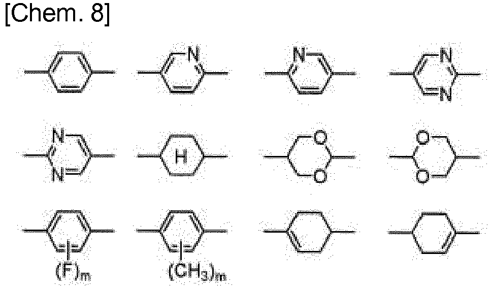 (où m représente un entier de 1 à 4) ;n4 représente 0 ou 1 ;Y1 et Y2 représentent chacun indépendamment une simple liaison, -CH2CH2-, -CH2O-, -OCH2-, -COO-, -OCO-, -C=C-, -CH=CH-, -CF=CF-, - (CH2)4-, -CH2CH2CH2O-, -OCH2CH2CH2-, -CH2=CHCH2CH2- ou - CH2CH2CH=CH- ;Y3 représente une simple liaison, -COO- ou -OCO- ; etR8 représente un groupe hydrocarboné ayant 1 à 18 atomes de carbone) et un composé représenté par la formule générale (X1c),
- Dispositif d'affichage à cristaux liquides selon la revendication 1 ou 2, dans lequel les électrodes de pixel ont des fentes.
- Dispositif d'affichage à cristaux liquides selon la revendication 1 ou 2, dans lequel au moins l'un du premier substrat et du second substrat a une structure pour spécifier une direction de pré-inclinaison.
- Dispositif d'affichage à cristaux liquides selon l'une quelconque des revendications 1 à 4, comprenant en outre un film de passivation prévu au moins soit entre le premier substrat et la couche de cristaux liquides, soit entre le second substrat et la couche de cristaux liquides.
- Dispositif d'affichage à cristaux liquides selon l'une quelconque des revendications 1 à 5, comprenant en outre un film de planarisation prévu au moins soit entre le premier substrat et la couche de cristaux liquides, soit entre le second substrat et la couche de cristaux liquides.
- Procédé de fabrication d'un dispositif d'affichage à cristaux liquides incluant une couche de cristaux liquides qui contient une composition de cristaux liquides et qui est maintenue entre un premier substrat comportant une électrode commune et une couche de filtre de couleur et un second substrat comportant une pluralité de pixels et des électrodes de pixel respectives, chacun des pixels ayant deux régions ou plus ayant des directions de pré-inclinaison différentes, le procédé comprenant les étapes consistant à :
maintenir, entre le premier substrat et le second substrat sans fournir de film d'alignement sur l'un des substrats ou les deux, une composition de polymérisation contenant des cristaux liquides contenant un composé représenté par la formule générale (I) ci-dessous
 (dans la formule, R3α représente un groupe alkyle ayant 1 à 8 atomes de carbone, un groupe alcényle ayant 2 à 8 atomes de carbone, un groupe alcoxy ayant 1 à 8 atomes de carbone ou un groupe alcényloxy ayant 2 à 8 atomes de carbone ; R4α représente un groupe alkyle ayant 1 à 8 atomes de carbone, un groupe alcényle ayant 4 à 8 atomes de carbone, un groupe alcoxy ayant 1 à 8 atomes de carbone, ou un groupe alcényloxy ayant 3 à 8 atomes de carbone; Q2 et Q3 représentent chacun indépendamment un groupe 1,4-phénylène ou un groupe trans-1,4-cyclohexylène ; G1 et G2 représentent chacun indépendamment une simple liaison, -CH2CH2-, -CH2O-, -OCH2-, -CF2O-, ou -OCF2- et I2 représente 0, 1 ou 2, et lorsque I2 est égal à 2, deux de chaque Q2 et G2 peuvent être identiques ou différents), un ou plusieurs composés de (méth)acrylate trifonctionnels ou plus, et un ou plusieurs composés de (méth)acrylate bi- ou monofonctionnels ; etpolymériser les deux composés polymérisables ou plus entre l'électrode de pixel et l'électrode commune par irradiation avec des rayons d'énergie active tout en appliquant une tension pour donner un angle de pré-inclinaison aux molécules de cristaux liquides dans la composition de polymérisation contenant des cristaux liquides et, en même temps, former une couche de commande d'alignement entre la couche de cristaux liquides et chacun du premier substrat et du second substrat en utilisant la composition de polymérisation contenant des cristaux liquides en tant que composition de cristaux liquides.
 - Procédé de fabrication d'un dispositif d'affichage à cristaux liquides selon la revendication 7, dans lequel le rayon d'énergie active est une lumière ultraviolette ayant une pluralité de spectres.
- Procédé de fabrication d'un dispositif d'affichage à cristaux liquides selon la revendication 7 ou 8, dans lequel les électrodes de pixel ont des fentes, ou au moins l'un du premier substrat et du second substrat a une structure pour spécifier une direction de pré-inclinaison.
Applications Claiming Priority (2)
| Application Number | Priority Date | Filing Date | Title |
|---|---|---|---|
| JP2015123850 | 2015-06-19 | ||
| PCT/JP2016/067217 WO2016204066A1 (fr) | 2015-06-19 | 2016-06-09 | Élément d'affichage à cristaux liquides et son procédé de fabrication |
Publications (3)
| Publication Number | Publication Date |
|---|---|
| EP3312667A1 EP3312667A1 (fr) | 2018-04-25 |
| EP3312667A4 EP3312667A4 (fr) | 2019-01-23 |
| EP3312667B1 true EP3312667B1 (fr) | 2019-08-21 |
Family
ID=57545605
Family Applications (1)
| Application Number | Title | Priority Date | Filing Date |
|---|---|---|---|
| EP16811541.8A Active EP3312667B1 (fr) | 2015-06-19 | 2016-06-09 | Dispositif d'affichage à cristaux liquides et son procédé de fabrication |
Country Status (7)
| Country | Link |
|---|---|
| US (1) | US20180142155A1 (fr) |
| EP (1) | EP3312667B1 (fr) |
| JP (1) | JP6132123B1 (fr) |
| KR (1) | KR20180019534A (fr) |
| CN (1) | CN107615149B (fr) |
| TW (1) | TWI697548B (fr) |
| WO (1) | WO2016204066A1 (fr) |
Families Citing this family (8)
| Publication number | Priority date | Publication date | Assignee | Title |
|---|---|---|---|---|
| TWI721283B (zh) * | 2013-02-06 | 2021-03-11 | 日商迪愛生股份有限公司 | 液晶顯示元件及其製造方法 |
| CN111164147B (zh) | 2017-10-02 | 2022-02-11 | 富士胶片株式会社 | 液晶组合物、反射层、反射层的制造方法及共聚物 |
| CN111771238B (zh) * | 2018-03-30 | 2022-08-30 | Jsr株式会社 | 显示装置及液晶取向剂 |
| TWI794515B (zh) * | 2018-07-03 | 2023-03-01 | 日商Dic股份有限公司 | 液晶顯示元件及液晶顯示元件之製造方法 |
| WO2020065713A1 (fr) * | 2018-09-25 | 2020-04-02 | 堺ディスプレイプロダクト株式会社 | Dispositif d'affichage à cristaux liquides |
| US10861209B1 (en) * | 2018-11-08 | 2020-12-08 | Michael Bruce | Unmanned aerial monitoring vehicle |
| CN112789344B (zh) * | 2018-12-12 | 2024-12-03 | 石家庄诚志永华显示材料有限公司 | 含聚合性化合物的液晶组合物、及液晶显示元件以及聚合性化合物 |
| CN111748356B (zh) * | 2020-07-24 | 2023-03-14 | 京东方科技集团股份有限公司 | 液晶组合材料及显示面板 |
Family Cites Families (15)
| Publication number | Priority date | Publication date | Assignee | Title |
|---|---|---|---|---|
| US6690441B2 (en) * | 2000-09-22 | 2004-02-10 | Dai Nippon Printing Co., Ltd. | Multi-domain vertical alignment mode liquid crystal display having spacers formed over zigzag like alignment-controlling projection |
| US8057701B2 (en) * | 2008-04-01 | 2011-11-15 | Adeka Corporation | Trifunctional (meth)acrylate compound and polymerizable composition containing same |
| CN102220140A (zh) * | 2010-04-16 | 2011-10-19 | 统炀企业有限公司 | 液晶配向组合物及制造液晶显示装置的方法 |
| KR101884035B1 (ko) * | 2010-07-15 | 2018-07-31 | 메르크 파텐트 게엠베하 | 중합체-안정화 호메오트로픽 정렬을 갖는 액정 매질 및 액정 디스플레이 |
| TWI425281B (zh) * | 2010-12-31 | 2014-02-01 | 友達光電股份有限公司 | 聚合物穩定配向型液晶顯示面板的製造方法 |
| US9249355B2 (en) * | 2011-02-05 | 2016-02-02 | Merck Patent Gmbh | Liquid-crystal displays having homeotropic alignment |
| US9677003B2 (en) * | 2012-03-30 | 2017-06-13 | Dic Corporation | Liquid crystal display device and method for producing the same |
| TWI635164B (zh) * | 2012-04-24 | 2018-09-11 | 迪愛生股份有限公司 | Liquid crystal composition containing polymerizable compound and liquid crystal display element using same |
| CN102660299B (zh) * | 2012-04-28 | 2015-02-04 | 深圳市华星光电技术有限公司 | 液晶介质混合物及使用其的液晶显示器 |
| US20130299741A1 (en) * | 2012-05-09 | 2013-11-14 | Shenzhen China Star Optoelectronics Technology Co. Ltd. | Liquid crystal medium composition |
| TWI565790B (zh) * | 2012-08-08 | 2017-01-11 | 捷恩智股份有限公司 | 液晶組成物、液晶顯示元件及液晶組成物的使用 |
| US9127198B2 (en) * | 2012-09-21 | 2015-09-08 | Shenzhen China Star Optoelectronics Technology Co., Ltd. | Mixture for liquid crystal medium and liquid crystal display using the same |
| TWI721283B (zh) * | 2013-02-06 | 2021-03-11 | 日商迪愛生股份有限公司 | 液晶顯示元件及其製造方法 |
| CN103484131B (zh) * | 2013-08-29 | 2016-08-10 | 深圳市华星光电技术有限公司 | 液晶介质组合物 |
| CN104597661B (zh) * | 2014-11-21 | 2017-06-27 | 深圳市华星光电技术有限公司 | 垂直配向液晶显示器及其制作方法 |
-
2016
- 2016-06-09 EP EP16811541.8A patent/EP3312667B1/fr active Active
- 2016-06-09 KR KR1020177034482A patent/KR20180019534A/ko not_active Withdrawn
- 2016-06-09 WO PCT/JP2016/067217 patent/WO2016204066A1/fr not_active Ceased
- 2016-06-09 US US15/579,437 patent/US20180142155A1/en not_active Abandoned
- 2016-06-09 JP JP2016555852A patent/JP6132123B1/ja active Active
- 2016-06-09 CN CN201680032505.3A patent/CN107615149B/zh active Active
- 2016-06-17 TW TW105119102A patent/TWI697548B/zh active
Non-Patent Citations (1)
| Title |
|---|
| None * |
Also Published As
| Publication number | Publication date |
|---|---|
| EP3312667A1 (fr) | 2018-04-25 |
| TWI697548B (zh) | 2020-07-01 |
| KR20180019534A (ko) | 2018-02-26 |
| EP3312667A4 (fr) | 2019-01-23 |
| TW201716552A (zh) | 2017-05-16 |
| JPWO2016204066A1 (ja) | 2017-06-29 |
| CN107615149B (zh) | 2020-10-27 |
| JP6132123B1 (ja) | 2017-05-24 |
| WO2016204066A1 (fr) | 2016-12-22 |
| US20180142155A1 (en) | 2018-05-24 |
| CN107615149A (zh) | 2018-01-19 |
Similar Documents
| Publication | Publication Date | Title |
|---|---|---|
| EP3312667B1 (fr) | Dispositif d'affichage à cristaux liquides et son procédé de fabrication | |
| EP2955570B1 (fr) | Elément d'affichage à cristaux liquides et son procédé de fabrication | |
| EP2770367B1 (fr) | Élément d'affichage à cristaux liquides et procédé de fabrication de celui-ci | |
| EP2701003B1 (fr) | Élément d'affichage à cristaux liquides | |
| EP2701002A1 (fr) | Élément d'affichage à cristaux liquides et procédé de fabrication de celui-ci | |
| JP6745814B2 (ja) | ネマチック液晶組成物及びこれを用いた液晶表示素子 | |
| KR20180130490A (ko) | 액정 표시 소자 및 그 제조 방법 | |
| WO2016093141A1 (fr) | Élément d'affichage à cristaux liquides, et procédé de fabrication de celui-ci | |
| WO2019216233A1 (fr) | Dispositif d'affichage à cristaux liquides | |
| JP6355009B1 (ja) | 液晶表示素子及びその製造方法 | |
| JP6296320B2 (ja) | 液晶表示素子及びその製造方法 | |
| JP6395007B2 (ja) | 液晶表示素子及びその製造方法 | |
| WO2017134841A1 (fr) | Élément d'affichage à cristaux liquides et son procédé de production |
Legal Events
| Date | Code | Title | Description |
|---|---|---|---|
| STAA | Information on the status of an ep patent application or granted ep patent |
Free format text: STATUS: THE INTERNATIONAL PUBLICATION HAS BEEN MADE |
|
| PUAI | Public reference made under article 153(3) epc to a published international application that has entered the european phase |
Free format text: ORIGINAL CODE: 0009012 |
|
| STAA | Information on the status of an ep patent application or granted ep patent |
Free format text: STATUS: REQUEST FOR EXAMINATION WAS MADE |
|
| 17P | Request for examination filed |
Effective date: 20171221 |
|
| AK | Designated contracting states |
Kind code of ref document: A1 Designated state(s): AL AT BE BG CH CY CZ DE DK EE ES FI FR GB GR HR HU IE IS IT LI LT LU LV MC MK MT NL NO PL PT RO RS SE SI SK SM TR |
|
| AX | Request for extension of the european patent |
Extension state: BA ME |
|
| DAV | Request for validation of the european patent (deleted) | ||
| DAX | Request for extension of the european patent (deleted) | ||
| A4 | Supplementary search report drawn up and despatched |
Effective date: 20181221 |
|
| RIC1 | Information provided on ipc code assigned before grant |
Ipc: C09K 19/56 20060101ALI20181217BHEP Ipc: G02F 1/13 20060101ALI20181217BHEP Ipc: G02F 1/1368 20060101ALI20181217BHEP Ipc: G02F 1/137 20060101ALI20181217BHEP Ipc: G02F 1/1337 20060101AFI20181217BHEP Ipc: G02F 1/1341 20060101ALI20181217BHEP Ipc: C09K 19/30 20060101ALI20181217BHEP Ipc: C09K 19/54 20060101ALI20181217BHEP Ipc: G02F 1/1343 20060101ALI20181217BHEP |
|
| GRAP | Despatch of communication of intention to grant a patent |
Free format text: ORIGINAL CODE: EPIDOSNIGR1 |
|
| STAA | Information on the status of an ep patent application or granted ep patent |
Free format text: STATUS: GRANT OF PATENT IS INTENDED |
|
| RIC1 | Information provided on ipc code assigned before grant |
Ipc: C09K 19/54 20060101ALI20190226BHEP Ipc: G02F 1/1343 20060101ALI20190226BHEP Ipc: C09K 19/56 20060101ALI20190226BHEP Ipc: G02F 1/1337 20060101AFI20190226BHEP Ipc: G02F 1/1341 20060101ALI20190226BHEP Ipc: C09K 19/30 20060101ALI20190226BHEP Ipc: G02F 1/13 20060101ALI20190226BHEP Ipc: G02F 1/1368 20060101ALI20190226BHEP Ipc: G02F 1/137 20060101ALI20190226BHEP |
|
| INTG | Intention to grant announced |
Effective date: 20190313 |
|
| GRAS | Grant fee paid |
Free format text: ORIGINAL CODE: EPIDOSNIGR3 |
|
| GRAA | (expected) grant |
Free format text: ORIGINAL CODE: 0009210 |
|
| STAA | Information on the status of an ep patent application or granted ep patent |
Free format text: STATUS: THE PATENT HAS BEEN GRANTED |
|
| AK | Designated contracting states |
Kind code of ref document: B1 Designated state(s): AL AT BE BG CH CY CZ DE DK EE ES FI FR GB GR HR HU IE IS IT LI LT LU LV MC MK MT NL NO PL PT RO RS SE SI SK SM TR |
|
| REG | Reference to a national code |
Ref country code: GB Ref legal event code: FG4D |
|
| REG | Reference to a national code |
Ref country code: CH Ref legal event code: EP |
|
| REG | Reference to a national code |
Ref country code: DE Ref legal event code: R096 Ref document number: 602016019177 Country of ref document: DE |
|
| REG | Reference to a national code |
Ref country code: AT Ref legal event code: REF Ref document number: 1170415 Country of ref document: AT Kind code of ref document: T Effective date: 20190915 |
|
| REG | Reference to a national code |
Ref country code: IE Ref legal event code: FG4D |
|
| REG | Reference to a national code |
Ref country code: LT Ref legal event code: MG4D |
|
| REG | Reference to a national code |
Ref country code: NL Ref legal event code: MP Effective date: 20190821 |
|
| PG25 | Lapsed in a contracting state [announced via postgrant information from national office to epo] |
Ref country code: FI Free format text: LAPSE BECAUSE OF FAILURE TO SUBMIT A TRANSLATION OF THE DESCRIPTION OR TO PAY THE FEE WITHIN THE PRESCRIBED TIME-LIMIT Effective date: 20190821 Ref country code: HR Free format text: LAPSE BECAUSE OF FAILURE TO SUBMIT A TRANSLATION OF THE DESCRIPTION OR TO PAY THE FEE WITHIN THE PRESCRIBED TIME-LIMIT Effective date: 20190821 Ref country code: SE Free format text: LAPSE BECAUSE OF FAILURE TO SUBMIT A TRANSLATION OF THE DESCRIPTION OR TO PAY THE FEE WITHIN THE PRESCRIBED TIME-LIMIT Effective date: 20190821 Ref country code: NO Free format text: LAPSE BECAUSE OF FAILURE TO SUBMIT A TRANSLATION OF THE DESCRIPTION OR TO PAY THE FEE WITHIN THE PRESCRIBED TIME-LIMIT Effective date: 20191121 Ref country code: PT Free format text: LAPSE BECAUSE OF FAILURE TO SUBMIT A TRANSLATION OF THE DESCRIPTION OR TO PAY THE FEE WITHIN THE PRESCRIBED TIME-LIMIT Effective date: 20191223 Ref country code: BG Free format text: LAPSE BECAUSE OF FAILURE TO SUBMIT A TRANSLATION OF THE DESCRIPTION OR TO PAY THE FEE WITHIN THE PRESCRIBED TIME-LIMIT Effective date: 20191121 Ref country code: LT Free format text: LAPSE BECAUSE OF FAILURE TO SUBMIT A TRANSLATION OF THE DESCRIPTION OR TO PAY THE FEE WITHIN THE PRESCRIBED TIME-LIMIT Effective date: 20190821 Ref country code: NL Free format text: LAPSE BECAUSE OF FAILURE TO SUBMIT A TRANSLATION OF THE DESCRIPTION OR TO PAY THE FEE WITHIN THE PRESCRIBED TIME-LIMIT Effective date: 20190821 |
|
| PG25 | Lapsed in a contracting state [announced via postgrant information from national office to epo] |
Ref country code: RS Free format text: LAPSE BECAUSE OF FAILURE TO SUBMIT A TRANSLATION OF THE DESCRIPTION OR TO PAY THE FEE WITHIN THE PRESCRIBED TIME-LIMIT Effective date: 20190821 Ref country code: LV Free format text: LAPSE BECAUSE OF FAILURE TO SUBMIT A TRANSLATION OF THE DESCRIPTION OR TO PAY THE FEE WITHIN THE PRESCRIBED TIME-LIMIT Effective date: 20190821 Ref country code: AL Free format text: LAPSE BECAUSE OF FAILURE TO SUBMIT A TRANSLATION OF THE DESCRIPTION OR TO PAY THE FEE WITHIN THE PRESCRIBED TIME-LIMIT Effective date: 20190821 Ref country code: GR Free format text: LAPSE BECAUSE OF FAILURE TO SUBMIT A TRANSLATION OF THE DESCRIPTION OR TO PAY THE FEE WITHIN THE PRESCRIBED TIME-LIMIT Effective date: 20191122 Ref country code: ES Free format text: LAPSE BECAUSE OF FAILURE TO SUBMIT A TRANSLATION OF THE DESCRIPTION OR TO PAY THE FEE WITHIN THE PRESCRIBED TIME-LIMIT Effective date: 20190821 Ref country code: IS Free format text: LAPSE BECAUSE OF FAILURE TO SUBMIT A TRANSLATION OF THE DESCRIPTION OR TO PAY THE FEE WITHIN THE PRESCRIBED TIME-LIMIT Effective date: 20191221 |
|
| REG | Reference to a national code |
Ref country code: AT Ref legal event code: MK05 Ref document number: 1170415 Country of ref document: AT Kind code of ref document: T Effective date: 20190821 |
|
| PG25 | Lapsed in a contracting state [announced via postgrant information from national office to epo] |
Ref country code: TR Free format text: LAPSE BECAUSE OF FAILURE TO SUBMIT A TRANSLATION OF THE DESCRIPTION OR TO PAY THE FEE WITHIN THE PRESCRIBED TIME-LIMIT Effective date: 20190821 |
|
| PG25 | Lapsed in a contracting state [announced via postgrant information from national office to epo] |
Ref country code: EE Free format text: LAPSE BECAUSE OF FAILURE TO SUBMIT A TRANSLATION OF THE DESCRIPTION OR TO PAY THE FEE WITHIN THE PRESCRIBED TIME-LIMIT Effective date: 20190821 Ref country code: PL Free format text: LAPSE BECAUSE OF FAILURE TO SUBMIT A TRANSLATION OF THE DESCRIPTION OR TO PAY THE FEE WITHIN THE PRESCRIBED TIME-LIMIT Effective date: 20190821 Ref country code: RO Free format text: LAPSE BECAUSE OF FAILURE TO SUBMIT A TRANSLATION OF THE DESCRIPTION OR TO PAY THE FEE WITHIN THE PRESCRIBED TIME-LIMIT Effective date: 20190821 Ref country code: DK Free format text: LAPSE BECAUSE OF FAILURE TO SUBMIT A TRANSLATION OF THE DESCRIPTION OR TO PAY THE FEE WITHIN THE PRESCRIBED TIME-LIMIT Effective date: 20190821 Ref country code: AT Free format text: LAPSE BECAUSE OF FAILURE TO SUBMIT A TRANSLATION OF THE DESCRIPTION OR TO PAY THE FEE WITHIN THE PRESCRIBED TIME-LIMIT Effective date: 20190821 Ref country code: IT Free format text: LAPSE BECAUSE OF FAILURE TO SUBMIT A TRANSLATION OF THE DESCRIPTION OR TO PAY THE FEE WITHIN THE PRESCRIBED TIME-LIMIT Effective date: 20190821 |
|
| PG25 | Lapsed in a contracting state [announced via postgrant information from national office to epo] |
Ref country code: CZ Free format text: LAPSE BECAUSE OF FAILURE TO SUBMIT A TRANSLATION OF THE DESCRIPTION OR TO PAY THE FEE WITHIN THE PRESCRIBED TIME-LIMIT Effective date: 20190821 Ref country code: SM Free format text: LAPSE BECAUSE OF FAILURE TO SUBMIT A TRANSLATION OF THE DESCRIPTION OR TO PAY THE FEE WITHIN THE PRESCRIBED TIME-LIMIT Effective date: 20190821 Ref country code: SK Free format text: LAPSE BECAUSE OF FAILURE TO SUBMIT A TRANSLATION OF THE DESCRIPTION OR TO PAY THE FEE WITHIN THE PRESCRIBED TIME-LIMIT Effective date: 20190821 Ref country code: IS Free format text: LAPSE BECAUSE OF FAILURE TO SUBMIT A TRANSLATION OF THE DESCRIPTION OR TO PAY THE FEE WITHIN THE PRESCRIBED TIME-LIMIT Effective date: 20200224 |
|
| REG | Reference to a national code |
Ref country code: DE Ref legal event code: R097 Ref document number: 602016019177 Country of ref document: DE |
|
| PLBE | No opposition filed within time limit |
Free format text: ORIGINAL CODE: 0009261 |
|
| STAA | Information on the status of an ep patent application or granted ep patent |
Free format text: STATUS: NO OPPOSITION FILED WITHIN TIME LIMIT |
|
| PG2D | Information on lapse in contracting state deleted |
Ref country code: IS |
|
| 26N | No opposition filed |
Effective date: 20200603 |
|
| PG25 | Lapsed in a contracting state [announced via postgrant information from national office to epo] |
Ref country code: SI Free format text: LAPSE BECAUSE OF FAILURE TO SUBMIT A TRANSLATION OF THE DESCRIPTION OR TO PAY THE FEE WITHIN THE PRESCRIBED TIME-LIMIT Effective date: 20190821 |
|
| PG25 | Lapsed in a contracting state [announced via postgrant information from national office to epo] |
Ref country code: MC Free format text: LAPSE BECAUSE OF FAILURE TO SUBMIT A TRANSLATION OF THE DESCRIPTION OR TO PAY THE FEE WITHIN THE PRESCRIBED TIME-LIMIT Effective date: 20190821 |
|
| REG | Reference to a national code |
Ref country code: CH Ref legal event code: PL |
|
| GBPC | Gb: european patent ceased through non-payment of renewal fee |
Effective date: 20200609 |
|
| PG25 | Lapsed in a contracting state [announced via postgrant information from national office to epo] |
Ref country code: LU Free format text: LAPSE BECAUSE OF NON-PAYMENT OF DUE FEES Effective date: 20200609 |
|
| REG | Reference to a national code |
Ref country code: BE Ref legal event code: MM Effective date: 20200630 |
|
| PG25 | Lapsed in a contracting state [announced via postgrant information from national office to epo] |
Ref country code: CH Free format text: LAPSE BECAUSE OF NON-PAYMENT OF DUE FEES Effective date: 20200630 Ref country code: LI Free format text: LAPSE BECAUSE OF NON-PAYMENT OF DUE FEES Effective date: 20200630 Ref country code: GB Free format text: LAPSE BECAUSE OF NON-PAYMENT OF DUE FEES Effective date: 20200609 Ref country code: IE Free format text: LAPSE BECAUSE OF NON-PAYMENT OF DUE FEES Effective date: 20200609 Ref country code: FR Free format text: LAPSE BECAUSE OF NON-PAYMENT OF DUE FEES Effective date: 20200630 |
|
| PG25 | Lapsed in a contracting state [announced via postgrant information from national office to epo] |
Ref country code: BE Free format text: LAPSE BECAUSE OF NON-PAYMENT OF DUE FEES Effective date: 20200630 |
|
| PG25 | Lapsed in a contracting state [announced via postgrant information from national office to epo] |
Ref country code: MT Free format text: LAPSE BECAUSE OF FAILURE TO SUBMIT A TRANSLATION OF THE DESCRIPTION OR TO PAY THE FEE WITHIN THE PRESCRIBED TIME-LIMIT Effective date: 20190821 Ref country code: CY Free format text: LAPSE BECAUSE OF FAILURE TO SUBMIT A TRANSLATION OF THE DESCRIPTION OR TO PAY THE FEE WITHIN THE PRESCRIBED TIME-LIMIT Effective date: 20190821 |
|
| PG25 | Lapsed in a contracting state [announced via postgrant information from national office to epo] |
Ref country code: MK Free format text: LAPSE BECAUSE OF FAILURE TO SUBMIT A TRANSLATION OF THE DESCRIPTION OR TO PAY THE FEE WITHIN THE PRESCRIBED TIME-LIMIT Effective date: 20190821 |
|
| P01 | Opt-out of the competence of the unified patent court (upc) registered |
Effective date: 20230324 |
|
| REG | Reference to a national code |
Ref country code: DE Ref legal event code: R082 Ref document number: 602016019177 Country of ref document: DE Representative=s name: WEIDNER STERN JESCHKE PATENTANWAELTE PARTNERSC, DE Ref country code: DE Ref legal event code: R081 Ref document number: 602016019177 Country of ref document: DE Owner name: SHIJIAZHUANG CHENGZHI YONGHUA DISPLAY MATERIAL, CN Free format text: FORMER OWNER: DIC CORPORATION, TOKYO, JP |
|
| PGFP | Annual fee paid to national office [announced via postgrant information from national office to epo] |
Ref country code: DE Payment date: 20250320 Year of fee payment: 10 |