EP3312871B1 - Dispositif de réception permettant de recevoir un empilement de substrat - Google Patents
Dispositif de réception permettant de recevoir un empilement de substrat Download PDFInfo
- Publication number
- EP3312871B1 EP3312871B1 EP17200753.6A EP17200753A EP3312871B1 EP 3312871 B1 EP3312871 B1 EP 3312871B1 EP 17200753 A EP17200753 A EP 17200753A EP 3312871 B1 EP3312871 B1 EP 3312871B1
- Authority
- EP
- European Patent Office
- Prior art keywords
- substrates
- heating
- substrate stack
- substrate
- bonding
- Prior art date
- Legal status (The legal status is an assumption and is not a legal conclusion. Google has not performed a legal analysis and makes no representation as to the accuracy of the status listed.)
- Active
Links
Images




Classifications
-
- H—ELECTRICITY
- H10—SEMICONDUCTOR DEVICES; ELECTRIC SOLID-STATE DEVICES NOT OTHERWISE PROVIDED FOR
- H10P—GENERIC PROCESSES OR APPARATUS FOR THE MANUFACTURE OR TREATMENT OF DEVICES COVERED BY CLASS H10
- H10P72/00—Handling or holding of wafers, substrates or devices during manufacture or treatment thereof
- H10P72/04—Apparatus for manufacture or treatment
- H10P72/0428—Apparatus for mechanical treatment or grinding or cutting
-
- H—ELECTRICITY
- H10—SEMICONDUCTOR DEVICES; ELECTRIC SOLID-STATE DEVICES NOT OTHERWISE PROVIDED FOR
- H10P—GENERIC PROCESSES OR APPARATUS FOR THE MANUFACTURE OR TREATMENT OF DEVICES COVERED BY CLASS H10
- H10P14/00—Formation of materials, e.g. in the shape of layers or pillars
- H10P14/40—Formation of materials, e.g. in the shape of layers or pillars of conductive or resistive materials
-
- H—ELECTRICITY
- H10—SEMICONDUCTOR DEVICES; ELECTRIC SOLID-STATE DEVICES NOT OTHERWISE PROVIDED FOR
- H10P—GENERIC PROCESSES OR APPARATUS FOR THE MANUFACTURE OR TREATMENT OF DEVICES COVERED BY CLASS H10
- H10P72/00—Handling or holding of wafers, substrates or devices during manufacture or treatment thereof
- H10P72/04—Apparatus for manufacture or treatment
- H10P72/0431—Apparatus for thermal treatment
- H10P72/0432—Apparatus for thermal treatment mainly by conduction
-
- H—ELECTRICITY
- H10—SEMICONDUCTOR DEVICES; ELECTRIC SOLID-STATE DEVICES NOT OTHERWISE PROVIDED FOR
- H10P—GENERIC PROCESSES OR APPARATUS FOR THE MANUFACTURE OR TREATMENT OF DEVICES COVERED BY CLASS H10
- H10P72/00—Handling or holding of wafers, substrates or devices during manufacture or treatment thereof
- H10P72/04—Apparatus for manufacture or treatment
- H10P72/0431—Apparatus for thermal treatment
- H10P72/0434—Apparatus for thermal treatment mainly by convection
-
- H—ELECTRICITY
- H10—SEMICONDUCTOR DEVICES; ELECTRIC SOLID-STATE DEVICES NOT OTHERWISE PROVIDED FOR
- H10P—GENERIC PROCESSES OR APPARATUS FOR THE MANUFACTURE OR TREATMENT OF DEVICES COVERED BY CLASS H10
- H10P72/00—Handling or holding of wafers, substrates or devices during manufacture or treatment thereof
- H10P72/06—Apparatus for monitoring, sorting, marking, testing or measuring
- H10P72/0602—Temperature monitoring
-
- H—ELECTRICITY
- H10—SEMICONDUCTOR DEVICES; ELECTRIC SOLID-STATE DEVICES NOT OTHERWISE PROVIDED FOR
- H10P—GENERIC PROCESSES OR APPARATUS FOR THE MANUFACTURE OR TREATMENT OF DEVICES COVERED BY CLASS H10
- H10P72/00—Handling or holding of wafers, substrates or devices during manufacture or treatment thereof
- H10P72/70—Handling or holding of wafers, substrates or devices during manufacture or treatment thereof for supporting or gripping
- H10P72/76—Handling or holding of wafers, substrates or devices during manufacture or treatment thereof for supporting or gripping using mechanical means, e.g. clamps or pinches
- H10P72/7602—Handling or holding of wafers, substrates or devices during manufacture or treatment thereof for supporting or gripping using mechanical means, e.g. clamps or pinches the wafers being placed on a robot blade or gripped by a gripper for conveyance
Definitions
- the present invention relates to a device and a method according to the independent claims.
- Alignment devices are known in which the alignment of the substrates to one another takes place under normal atmosphere.
- the aligned substrates are temporarily fixed together in the alignment device and then transferred to a high vacuum bonding device and permanently bonded there under vacuum, with the temperature required for bonding being generated by heat sources.
- the heat sources and the associated pressure plates are located above and below the substrates to be bonded.
- the upper heat source and the upper pressure plate are designed to be movable.
- the lower heat source and the sample holder at the bottom of the high vacuum bonding device are designed to be static.
- the two substrates to be aligned are fixed to a sample holder (bond chuck). Fixing is usually done with mechanical clamps. The The substrates, which are held in the sample holder and aligned with each other, are then transported to the high vacuum bonding device. The sample holder is placed on the lower heat source.
- the object of the present invention is therefore to provide a device or a method with which the problems of the prior art are solved.
- the basic idea of the present invention is to heat the substrates of the substrate stack aligned with contact surfaces of the substrates for, in particular, permanent, bonding in the bonding device gently and evenly from both surfaces to be heated (the sides facing away from the contact surfaces) of the substrates in order to minimize or completely avoid, in particular, different deformations of the two substrates.
- the invention is particularly applicable to a modularized device and a process chain which makes it possible to use an alignment device for aligning and temporarily connecting two or more substrates to form a substrate stack.
- the substrates aligned therein are transferred to a bonding device via a high vacuum transfer line (i.e. without interrupting the vacuum) taking into account particularly sensitive handling.
- the substrates are permanently and inseparably (i.e. permanently) joined (bonded) without exposing the substrates to excessive or varying stretching and distortion.
- the alignment device is designed such that connecting elements that do not contaminate the substrate stack and temporarily hold the substrate stack together are provided for fixing the substrate stack in the alignment unit before transfer to a bonding unit.
- the connecting elements can be removed without leaving any residue after bonding.
- the substrate stack is processed within a vacuum transfer line with one or more devices for reducing surface gases and/or moisture to improve the bonding result.
- the substrate stack is or can be heated symmetrically.
- the contact surfaces of the substrates of the substrate stack serve as the plane of symmetry.
- the substrate stack is heated equithermally from both sides.
- the following description therefore deals in particular with a method and a Device for heating and bonding a substrate stack.
- the heating is preferably carried out symmetrically, in particular by infrared radiation.
- the components according to the invention are part of a, in particular modularized constructed system, in particular a high vacuum cluster.
- a process chain up to the bonding of a substrate stack can be carried out.
- special attention is paid to the sensitive handling of the substrates to be bonded.
- the sensitive handling particularly concerns a uniform, in particular symmetrical, introduction of heat into the substrates to be treated through different heating zones, which is preferably achieved by an upper dynamically movable heating device and associated sample holder (English: chucks) and a lower, in particular rigid or static, heating device.
- a particularly gentle bonding process is made possible by controlled movement of the upper heating device towards the lower heating device.
- the process steps are preferably carried out while maintaining the vacuum generated in the alignment unit, in particular during transport through the vacuum transfer section with a vacuum transfer chamber, in particular a high vacuum transfer chamber.
- a device in particular a high vacuum bonding device
- a symmetrical heat input preferably by evenly bringing the opposite heating surfaces of the heating devices towards the substrates to be processed, to control the heat input of the substrates depending on their material type and their thickness and/or taking into account the expansion coefficient in order to avoid different deformations, in particular expansions and/or distortions, in particular when using different types of materials.
- the symmetrical heating serves the uniform (i.e. homogeneous) heating of both sides of the substrate stack.
- the heating rate defines by how many degrees the substrate heats up per unit of time.
- the heating rate is set to a value between 1 °C/min and 1000 °C/min. Smaller heating rates would be possible, but are no longer economical at the desired temperatures because the heating process would take too long. Heating rates greater than 1000 °C/min would heat the substrates so quickly that they could cause damage to the substrates and/or alignment errors between the substrates.
- the heating power indicates the amount of heat per unit of time that is required to heat an object to a specified temperature.
- the heating power is applied by heating elements, particularly those arranged in the sample holders, which are mainly operated electrically. Assuming ideal conditions, i.e.
- a lower limit of the necessary (electrical) power can be calculated, which is the minimum required to bring a substrate with a certain diameter and thickness to the desired temperature within a desired time.
- the heating power corresponds to the energy introduced into a substrate per unit of time.
- the energy introduced corresponds in particular to the heat introduced.
- the heat required to heat a body from an initial temperature to a final temperature corresponds to the product of the temperature difference to be overcome, the specific heat capacity and the mass of the body.
- the mass of the body can be calculated for a given density and dimensions. Substrates are preferably round and very often single crystals. Therefore, they have geometries that can be calculated and a homogeneous density.
- the calculation of the mass as a function of the geometric parameters, in particular the thickness and diameter, can The amount of heat determined in this way is then divided by the desired minimum time in which the corresponding temperature difference is to be overcome. This gives the heating output. The electrical output is then selected accordingly. Since not all of the electrical output is converted into thermal output, the electrical output actually to be introduced is selected to be correspondingly higher in order to compensate for the power loss.
- the table shows the minimum electrical power required to heat a silicon substrate with a diameter of 200 mm and a thickness of 725 ⁇ m from 25 °C to 525 °C in the given times.
- the actual electrical power is calculated based on power losses. be greater.
- the electrical power of the heaters used is in particular chosen to be greater than 100 W, preferably greater than 1000 watts, even more preferably greater than 5000 watts, most preferably greater than 10000 watts, most preferably greater than 20000 watts.
- the first substrate is subjected to pressure in particular by a first pressure surface of a first pressure plate, which is preferably simultaneously the first heating surface.
- the second substrate is subjected to pressure in particular by a second pressure surface of a second pressure plate, which is preferably simultaneously the second heating surface.
- recipes or processes that are to be determined and specified in advance are used, which preferably take into account material-specific properties and/or the concrete nature, in particular the material thickness, of the substrates to be bonded.
- semi-automatic use of the device and also manual use of the device in question are also conceivable.
- the substrates to be bonded are made of materials that reflect thermal radiation very strongly and thus significantly slow down or make it more difficult to introduce the desired heat, the recipes are adjusted accordingly. Conversely, however, increased absorption of thermal radiation through correspondingly strongly absorbing materials and/or surface properties would also be conceivable, whereby the recipes, in particular heating times, would be shortened accordingly.
- the device is particularly capable of detecting factors influencing heating, in particular through sensors. recognize and take into account in the process flow and/or control in subsequent steps or subsequent substrate stacks.
- the device also preferably makes it possible to advantageously treat the substrates by convection and/or different heating zones, so that a uniform introduction of heat is achieved.
- the heating of the substrates preferably takes place via convection of a gas introduced into the bonding device, in particular into the sample holder, even more preferably a studded sample holder (in particular disclosed as an independent aspect of the invention). While the gas ensures the heat transfer by convection, the bonding device is evacuated, preferably continuously, so that a pressure of less than 10 -2 mbar, even more preferably less than 10 -3 mbar, is established in the bonding chamber. The gas is introduced in particular before and/or during an evacuation of the bonding device.
- the gas can be guided from the outside, preferably through a line of the sample holder and/or a pressure plate to the substrate stack and/or sample holder or pressure plate.
- the gas is distributed optimally between the substrate holder and/or the printing plate and the substrate stack due to the defined topography.
- the aligned substrate stacks are in the bonder (in particular on a stud chuck) and the area around the substrates is evacuated, a gas flows (in particular from the stud chuck) which ensures heat conduction between the (stud) sample holder and the substrate stack.
- the outside is evacuated and flushing takes place between the substrate stack and the (stud) sample holder. The flushing reduces the pressure in the bonding chamber created by the vacuum device accordingly.
- One of the most important aspects of the invention is to prevent the substrates from shifting relative to one another when they are heated, which would cause the substrates to lose their alignment with one another. From a physical point of view, the challenge is to ensure that the thermal expansion of both substrates that occurs when the temperature changes is always the same. If both substrates are made of the same material, the two substrates are preferably heated to the same temperature.
- the heating devices are controlled during heating and approach in such a way that, at least for the majority of the approach, the difference between the average temperature of the first substrate and the average temperature of the second substrate is less than 5°C, in particular less than 1°C, preferably less than 0.5°C, even more preferably less than 0.1°C. If the two substrates aligned with each other are made of the same material but have different thicknesses, it can happen that the temperature change in one of the two substrates, in particular in the substrate with the greater thickness, is slower than in the other substrate, in particular the one with the lesser thickness. In such a situation, the two substrates can therefore shift during the heating process despite the same material properties but different geometry properties.
- the alignment previously created by an alignment unit would be correctly adjusted again. If the materials and thus the material properties of the two substrates, in particular the thermal expansion coefficient or the thermal expansion tensor and/or the thermal conductivity and/or the heat capacity, are different, an unwanted shift of the substrates relative to each other occurs. This can be compensated.
- the heating devices are controlled during heating and the approach in such a way that at least during the for the majority of the approach, the difference between the average temperature of the first substrate and the average temperature of the second substrate is greater than 0.1°C, in particular greater than 0.5°C, preferably greater than 1°C, even more preferably greater than 5°C, in order to compensate for the difference in the thermal expansion of the two substrates, so that the alignment is maintained as well as possible.
- the heating devices during heating and approach such that the radiation energy of the first heating surface impinging on the first surface during approach is the same as the radiation energy of the second heating surface impinging on the second surface.
- an improvement in the bonding result is achieved by heating the substrates prior to bonding and thus outgassing, especially within the vacuum transfer section and before reaching the actual bonding device.
- the substrates are preferably heated uniformly or homogeneously (symmetrical or asymmetrical) to suit the individual requirements. This largely avoids (thermal) stresses caused by uneven expansion within the substrates, which has a positive effect on the desired bonding result.
- the thermal expansion coefficient of silicon for example, is in the range of 2.6 10 -6 K -1 . If both substrates are made of silicon, they both have the same (average) thermal expansion coefficient (assuming that both substrates have the same crystal orientation, which can usually be assumed since most silicon wafers have a crystallographic (100) orientation and assuming that the thermal Expansion in the substrate plane is isotropic). Accordingly, substrates subjected to the same thermal load will also experience the same thermal expansion. If the materials differ, their thermal expansion coefficients are generally different. These different thermal expansions can be compensated according to the invention.
- a receiving device for receiving the substrate stack at least during bonding.
- the receiving device is particularly suitable for receiving the substrate stack, in particular on the circumference or in a peripheral region.
- the receiving device is also preferably suitable for holding the substrates together at the contact surfaces and keeping them in the aligned position until the substrates are bonded.
- the receiving device in particular the nub sample holder, preferably acts on or contacts only a small section of the surfaces of the substrates facing away from the contact surfaces.
- the receiving device hardly covers or does not cover the surface of the substrates to be exposed to radiant heat. In other words, the majority, in particular at least 3 ⁇ 4, preferably at least 90%, of the surfaces of the substrates are exposed to the heating surfaces of the heating devices arranged at a distance therefrom.
- the substrate stack is heated on both sides at least during the Heating up to the bonding temperature takes place at least predominantly by thermal radiation and/or thermal convection, in particular by natural thermal convection. This is achieved in particular by spacing the surfaces of the substrates from the heating surfaces.
- the heat output introduced by thermal radiation increases in relation to the heat output introduced by thermal convection.
- the heat output is transferred at least partially, preferably predominantly, by thermal conduction between the surfaces and the heating surfaces.
- the bonding temperature is reached at least 3 ⁇ 4 of the way before thermal conduction and/or pressure is applied.
- a possible heat convection from above and below has the advantage that existing unevenness that makes uniform and advantageous heating of the substrates difficult during the bonding process can be greatly reduced or completely eliminated.
- these have nubs in order to achieve the lowest possible contamination of the surfaces of the substrates. This also makes it possible to supply the gas required for convection even during pressurization.
- the contact surfaces of the knobs can in particular be cambered in order to further reduce the contact area of the heating surfaces to the surfaces of the substrates.
- the dimple surface is further developed by covering the entire radial peripheral area of the heating surface or pressurization area is limited by a sealing ring.
- the peripheral area of the upper and lower studded pressure plate forms a positive fit with the substrate to be processed and thus prevents the gas from escaping.
- Process-accelerating measures such as the contamination-reducing automated transfer of the substrates aligned in the alignment unit by a process robot located within a vacuum transfer line with a specially designed holding device, particularly in the form of a support that only touches the substrate on the radial circumference, are not yet known.
- This holding device can also be subjected to an electrostatic force in order to further increase the holding forces of the process robot.
- Processes prior to and/or subsequent to alignment are also considered advantageous in order to remove surface gases and/or moisture before introduction into the vacuum bonding device and thus improve the bonding result.
- a further advantage is the increase in the precision of a bonding process. This means that the positioning accuracy of several structures of the substrates relative to one another achieved by the alignment unit is not lost due to the heat treatment in the bonder.
- deformations occur in particular when inhomogeneously heated substrate stacks, for example due to substrates made of different materials and thus different thermal expansion coefficients, shift or deform before the bonding process is completed, i.e. the process of applying pressure begins or takes place.
- the invention allows the alignment accuracy of the alignment device to be maintained between several structures up to and beyond the actual bonding process. The alignment accuracy achieved and maintained, i.e.
- the maximum shift between the structures on the opposite substrates of the aligned substrate stack until the bonding is completed is according to the invention in particular less than 10 ⁇ m, preferably less than 1 ⁇ m, more preferably less than 100 nm, most preferably less than 10 nm.
- an increase in throughput can be achieved because the heaters and thus the sample holder and the printing plates are preferably not constantly heated and cooled, but can, in particular at least predominantly, preferably exclusively, cause a temperature change on the substrate stack by changing position.
- Components of the bonder, in particular at least one of the printing plates, can move into a standby position at full bonding temperature and wait there for the next substrate stack without having to be cooled.
- a studded sample holder is preferably used, in particular as a pressure plate and/or heating surface, which minimizes the effective contact area with the substrates even when pressure is applied.
- the contact area of the studded sample holder is in particular less than 90%, preferably less than 50%, more preferably less than 25%, most preferably less than 5%, most preferably less than 1% of the substrate area.
- the device consists in particular of a modular device/system, which in a first embodiment consists of at least three modules that can be controlled independently of one another, namely an alignment unit (English: aligner), a vacuum transfer section with integrated handling device, in particular the process robot for handling substrates, and a bonding unit.
- an alignment unit English: aligner
- a vacuum transfer section with integrated handling device in particular the process robot for handling substrates
- a bonding unit for process-related reasons, it is possible to add further modules.
- some modules can be provided multiple times for acceleration and parallel processing.
- the loading of the alignment unit with the at least two substrates to be aligned is done manually, but can preferably be done semi-automatically or, even more preferably, fully automatically.
- the substrates are preferably wafers.
- the wafers are standardized semiconductor substrates with well-defined, standardized diameters.
- the substrates can have any shape. In particular, the substrates can be rectangular or round. If the substrates are round, the diameters of the substrates can also be any can be of any size, but usually have one of the standardized diameters of 1, 2, 3, 4 inches and 125, 150, 200, 300 or 450 mm.
- substrates are referred to in general.
- the embodiments according to the invention relate primarily to wafers.
- the substrates are aligned with one another and form a substrate stack.
- the substrate stack consists of at least two substrates. However, more than two, preferably more than five, more preferably more than ten, and most preferably more than 15 substrates can be aligned with one another and temporarily connected to form a substrate stack.
- the substrates can be made of any material. Preferably they are materials that are used in the semiconductor industry. These preferably include semiconductors such as silicon, germanium, glasses such as quartz, semiconductor heterostructures such as GaAs or ceramics. The use of polymer substrates or metal substrates would also be conceivable.
- the thicknesses of the substrates vary between 10,000 ⁇ m and 50 ⁇ m, with substrates with correspondingly low thicknesses being produced to the respective thickness using grinding and polishing processes.
- Carrier substrates that only serve to support other substrates, the so-called product substrates have high thicknesses, whereas product substrates are increasingly thinned in order to achieve a correspondingly high packing density of functional units on the product substrates by stacking.
- the thickness of a carrier substrate is greater than 200 ⁇ m, preferably greater than 500 ⁇ m, most preferably greater than 700 ⁇ m, most preferably greater than 1000 ⁇ m.
- the thickness of a product substrate is less than 1000 ⁇ m, preferably less than 500 ⁇ m, more preferably less than 100 ⁇ m, most preferably less than 50 ⁇ m.
- the alignment unit is also equipped with a device for receiving and fixing the substrates, which allows substrates to be fixed to each other after alignment.
- the alignment unit comprises a device that allows substrates to be aligned with one another and to be temporarily fixed with a fixing agent in such a way that transport from the alignment unit via a vacuum transfer path to another module, in particular a bonding device, is possible without this transport having a negative effect on the aligned substrates.
- the fixing unit is a device for magnetically fixing the substrate stack, as in the publication PCT/EP2013/056620 described, to which reference is made in this respect.
- the clamping is carried out by mechanical clamps which clamp the sides of the substrates in a small circumferential section and no longer have to be fixed to a sample holder.
- the individual modules are equipped with connecting locks, which are located at the respective transitions to the individual modules and which make it possible to to create defined atmospheres that positively influence the further process.
- a lock is an area, in particular a room, which is connected by two lock gates to two other areas, in particular rooms, which are separate from one another but connected to the lock. Access from and/or from the lock into and/or from one of the two rooms is via lock gates.
- the lock gates can be controlled individually.
- the lock gates are designed in particular as valves or gate valves. In the following, no explicit distinction is made between lock gate and/or lock. This means that when the word lock gate is used, it can also mean an entire lock, and therefore an area, in particular a room, with two lock gates.
- the substrates can be heated to preferably >100°C before being introduced into the alignment unit.
- the free path length for molecules on the surface can be maximized.
- the substrates can be heated at a large distance from a chamber wall (>1cm, >5cm, >10cm). The resulting large free path promotes the removal of foreign atoms and gases from the surface of the substrates.
- the temperatures preferably fall back to room temperature.
- the alignment of the substrates takes place in the alignment unit in particular under high vacuum conditions, which preferably correspond essentially to the pressure conditions in the bonding device.
- an automated transport takes place via a process robot from the alignment unit to a vacuum transfer module, in which preparatory measures can be carried out for the bonding planned in the further course of the process.
- the robot places the substrate stack on extendable loading pins. There is only partial direct contact between the loading pins and the substrate stack.
- a maximum of thirty, preferably less than 20, more preferably less than 10, most preferably less than 5, most preferably exactly three loading pins are used.
- the substrate stack to be bonded thus floats between a first heating surface and pressure plate that can be dynamically brought up to the substrates and a second heating surface, which is particularly static.
- Both the first (particularly upper) and the second (particularly lower) heating device and pressure plate advantageously have approximately the same diameter as the substrates to be treated, or are larger.
- the first heating surface and pressure plate can be brought up to the substrates both symmetrically and asymmetrically.
- the distance is not equal to the distance of the second heating surface and Printing plate to the substrate holder located between the first and second heating surface or to the surfaces of the substrates to be heated.
- the distance between the first and/or second heating surface and the substrate stack during the loading process is in particular greater than 1 mm, preferably greater than 5 mm, more preferably greater than 10 mm, most preferably greater than 30 mm.
- the temperatures of the first and/or second heating surface during the loading process are in particular greater than 25°C, preferably greater than 100°C, more preferably greater than 300°C.
- the heating rate of the substrate stack is controlled in particular by the distances A of the first heating surface and/or B of the second heating surface relative to the substrate stack or to the respective surfaces. This makes it possible in particular to run temperature programs and/or cycles without having to constantly cool or heat the heating devices and thus the sample holder and/or the printing plate.
- a similar procedure has already been described in the patent specification EP2013/064151 used to heat a liquid by positioning a heater without having to constantly heat or cool the heater.
- This embodiment according to the invention makes it possible to heat a heater to a certain, in particular bonding temperature, but to set its position so far from the loading level of the substrate stack during the loading process that the loaded substrate stack is initially hardly heated (i.e. in particular during loading).
- the distance A during dynamic movement of the first heating surface and pressure plate towards the substrates is equal to the distance B of the second, in particular static, second heating surface.
- This is achieved in particular by controlled and in particular continuous movement of the first heating surface towards the second heating surface, whereby at the same time the receiving device receiving the substrate stack is also moved towards the second heating surface.
- the first heating surface is moved towards the second heating surface exactly twice as fast as the substrate stack.
- the receiving device with the substrate stack remains stationary and the two heating surfaces move, in particular at the same speed and at equal, symmetrically decreasing distances A and B, from above and below towards the substrate stack.
- recipes are stored in a control device, which ensure optimized heating of the substrates while taking existing parameters into account.
- the main parameters to be considered are the type of material, thickness, heating temperature and bonding process.
- the asymmetric approach or positioning has the main purpose of enabling a different heat input into the substrates in order to compensate for the thermal expansion of two substrates made of different materials.
- each material has its own thermal expansion coefficient.
- the The substrate with the larger thermal expansion coefficient is heated to a lower temperature than the substrate with the lower thermal expansion coefficient. According to the invention, this can be achieved by different temperatures on the first heating surface and the second heating surface and/or by different distances A and B.
- Another aspect is that gas entry between the contact surfaces of the substrate stack is prevented after contacting the first printing plate and the second printing plate or the sample holder with the substrate stack and a gas is then introduced into the bonding device. This spreads between the rough surface of the substrate stack and the sample holder or the printing plates and thermally closes the surface irregularities.
- Thermal closure means that the introduced gas serves as a heat exchanger in order to transfer the heat from the heaters via the sample holder or the pressure plate into the substrate stack as quickly as possible.
- the gas pressure between the sample holder and the substrate stack is in particular >0.01 mbar, preferably >0.1 mbar, very preferably >1 mbar, most preferably >3 mbar. This gas pressure is achieved in particular by small gas quantities (flow rate), preferably >1 sccm, even more preferably >5 sccm, even more preferably >20 sccm.
- a high vacuum can be maintained in the bonding chamber at the same time, in particular ⁇ 0.001 mbar, preferably ⁇ 0.0001 mbar, even more preferably ⁇ 0.00001 mbar.
- a force acts on the substrate stack that prevents lateral displacement.
- the bonding forces applied are preferably between 1 N and 200 kN, with greater preference between 1 kN and 100 kN.
- a nub sample holder is a sample holder whose surface is not flat, but consists of several small elevations, the nubs, which form a holding plane and support the substrate stack on it. These nubs significantly reduce the contact surface to the substrate stack and thus also reduce the probability of contamination of the substrate.
- the nub sample holder is designed in such a way that it can withstand the applied bonding force.
- the height of the nubs is in particular less than 1 mm, preferably less than 0.1 mm, more preferably less than 0.01 mm, most preferably less than 0.001 mm. It is particularly preferable that the pressure plate also has nubs, so that the pressure plate is a nub pressure plate which has the same inventive property as the nub sample holder.
- At least one of the heating devices preferably the one that is also designed as a sample holder, has a heating surface consisting of several zones. These zones of the heating surface can preferably be controlled individually.
- the zones of the heater are preferably circular rings positioned concentrically to one another. By specifically controlling the zones, locally resolved Temperature profiles are generated.
- the number of zones is greater than 1, preferably greater than 5, more preferably greater than 10, most preferably greater than 20, most preferably greater than 50, most preferably greater than 100.
- modules described are those in which special atmospheres can be reproducibly produced depending on the material of the substrates and the requirements for the respective bonding process.
- the modules can be regulated independently of one another, in particular continuously.
- the individual modules can also be operated without a vacuum, i.e. at normal pressure. Atmospheric synchronization of two adjacent modules is also possible in order to enable accelerated movement of substrates from one module to a module downstream within the process.
- the pressure within the vacuum section and/or within the alignment device and/or within the bonding device is in particular less than 1 mbar, preferably less than 10 -3 mbar, more preferably less than 10 -5 mbar, most preferably less than 10 -7 mbar, most preferably less than 10 -9 mbar.
- the approach to the heating surfaces takes place symmetrically to the substrate stack, in particular symmetrically to the surfaces and/or symmetrically to the contact surfaces, and/or with the same temperature of the heating surfaces.
- heating surfaces are each larger than the surfaces of the substrate stack facing the heating surfaces.
- the first heating surface or the second heating surface is not moved when approaching.
- the heating devices are controlled during heating and approaching in such a way that at least during the predominant duration of the approaching, the difference between the average temperature of the first substrate and the average temperature of the second substrate less than 5°C, in particular less than 1°C, preferably less than 0.5°C, even more preferably less than 0.1°C.
- the substrate stack is preheated before being arranged between the heating surfaces, in particular outside a bonding chamber of a bonding device that encloses the heating devices, in particular in a vacuum-sealed manner.
- the arrangement of the substrate stack between the heating surfaces and/or the heating and/or the approach and/or the formation of the permanent bond takes place in a vacuum.
- the heating devices are controlled during heating and approaching in such a way that the radiation energy of the first heating surface impinging on the first surface during approaching is the same as the radiation energy of the second heating surface impinging on the second surface.
- first heating surface and/or the second heating surface are formed by knobs with flow channels running between the knobs for the application, in particular flow through, of a gas.
- the flow channels are surrounded, in particular enclosed, by a, in particular annular, web for sealing the flow channels to the first and/or second substrate.
- the web has an opening for the controlled discharge of the gas.
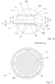
- FIG 12 a top view of a studded pressure plate.
- identical or equivalent features are identified by the same reference numerals.
- the Figure 1a shows a schematic plan view of a system 38, designed in particular as a vacuum cluster, preferably as a high vacuum cluster.
- the system 38 consists of exactly two modules attached to a vacuum transfer chamber 4, a module with an alignment device 1 and a module with a bonding device 6 according to the invention.
- a robot 34 designed in particular as a process robot, removes (here identical) substrates 35, 36 from a loading container 39 and transports the first substrate 35 and the second substrate 36, in particular simultaneously, along a vacuum transfer path 5 into the alignment unit 1.
- the loading container 39 can in particular also be a lock or act as such.
- the two substrates 35, 36 are aligned with each other and fixed, in particular temporarily, to a first contact surface 35k of the first substrate 35 and a second contact surface 36k of the second substrate 36 to form a substrate stack 14.
- the systems from the patent documents could be used as an alignment unit, for example.
- PCT/EP2013/075831 or from PCT/EP2013/062473 Optimal alignment is achieved when the structures to be aligned are in particular the alignment marks, fit together optimally according to the overlay model known in the industry. A corresponding description of such an overlay model can be found in the patent specification PCT/EP2013/061086 .
- the robot 34 then transports the fixed and aligned substrate stack 14 into the bonding device 6, in particular by picking it up on a first surface 35o of the first substrate 35 or on a second surface 36o of the second substrate 36.
- the surfaces 35o, 36o each face away from the contact surfaces 35k, 36k.
- Annex 38' shows a vacuum cluster consisting of several modules connected by a vacuum transfer chamber 4'.
- the modules can differ from one another in terms of their functionality.
- modules for heating or cooling substrates or substrate stacks, cleaning modules, plasma modules, coating modules with spin coaters or spray coaters, bonders 1 and debonders, coating modules, alignment modules 6 are conceivable.
- the modules are preferably arranged in a circle or star shape around a vacuum transfer chamber 4'.
- the vacuum transfer chamber 4' is connected to the various modules via valves 2.
- the modules and the vacuum transfer chamber 4' can be evacuated independently of one another via the valves 2, but are preferably always at the same vacuum level, preferably the high vacuum level of the bonding device 6.
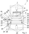
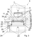
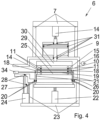
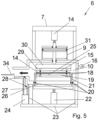
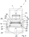
- the bonding device 6 is in the Figures 2 to 9 shown in different processing states.
- the bonding device 6 is built on a static support structure 23 in the form of a base plate and columns fixed to the base plate.
- the bonding chamber 10 is fixed to the columns.
- the bonding chamber 10 has a chamber opening 6o which can be closed with the valve 2 for loading the bonding chamber 10.
- the valve 2 is formed from a lock drive 24 supported on the base plate, in particular in the form of an actuator.
- the lock drive 24 serves to open and close a lock gate 27 driven by the lock drive 24, which opens and closes the chamber opening 6o through a slot 6s.
- the valve 2 has seals 28 for sealing the bonding chamber 10 from the environment when the valve 2 is closed.
- the bonding device 6 comprises a receiving device 18 for receiving the substrate stack 14.
- the receiving device 18 comprises a substrate support with a support plane E, on which the substrate stack 14 is placed with the second surface 36o, so that the second surface 36o lies in the support plane E.
- the substrate support is formed by at least two loading pins 21 penetrating the bonding chamber 10, in the embodiment shown four loading pins 21.
- the bonding chamber 10 is sealed from the surroundings of the bonding chamber 10 by seals 20 enclosing the loading pins 21.
- the seals 20 also serve to guide the loading pins 21 in a sliding, translational manner.
- the loading pins 21 are fixed on a, in particular common, positioning plate 21p.
- the loading pins 21 are preferably mechanically coupled to one another by the positioning plate 21p and are connected to one another by a in particular centrally acting actuator 22, preferably in the form of a single, alternatively by means of several loading pin actuator(s), moved translationally transversely to the support plane E.
- a second heating device 26 for heating the second surface 36o and a second pressure plate 25 fixed to the second heating device 26, in particular over the entire surface, are arranged within the loading pins 21.
- the second pressure plate 25 has a second heating surface 19 which can be arranged below the support plane E parallel to it.
- the heating device 26 and the pressure plate 25 are fixedly connected to the bonding chamber 10 and are static, i.e. cannot move relative to the support plane E.
- a first heating surface 15 can be arranged parallel to the support plane E and above it.
- the first heating surface 15 is arranged on a first pressure plate 29, which in turn is fixed to a first heating device 30, in particular over its entire surface.
- the heating device 30 is adjustable transversely to the support plane by drive means.
- the heating device 30 is fixed to an adjusting rod that passes through the bonding chamber 10.
- the adjusting rod is moved at the end opposite the heating device 30 by a position actuator 8 to control the position, in particular a distance A of the first heating surface 15 to the first surface 35o, of the first heating surface 15.
- a force actuator 9 is used to apply pressure, in particular after contacting the first surface 35o with the first heating surface 15 and the contacting of the second surface 36o with the second heating surface 19.
- the bonding chamber 10 is sealed from the environment by seals 31 that seal the drive means.
- the drive means are suspended from a supporting structure 7, consisting of a ceiling plate and columns supporting the ceiling plate.
- the robot 34 with the substrate stack 14 is moved, in particular introduced, into a bonding chamber 10 of the bonding device 6.
- the receiving device 18 according to the invention for receiving the substrate stack 14 is at a starting height.
- the substrate stack 14 is preferably positioned symmetrically to the first heating surface 15 and the second heating surface 29 with respect to the contact surfaces 35k, 36k. This symmetrical starting position is particularly important when the second printing plate 25 and/or the first printing plate 29 have been preheated by their corresponding heating devices 26, 30.
- a fourth step according to the invention Figure 5 the robot 34 is removed from the bonding chamber 10 and the lock 27 is closed. After closing, the interior of the bonding device 6 can be evacuated to an even higher vacuum via a pump 16 if the vacuum prevailing in the adjacent vacuum transfer chamber 4 is set too low for the bonding process.
- Heating is achieved by heat output generated by the heating devices 26, 30 and emitted via the heating surfaces 15, 19 as radiant heat 17.
- the temperature fields above and below the substrate stack 14 can be set completely equivalently, provided that the two heating devices 26, 30 are controlled with the same power and the same parameters and the printing plates 25, 29 have the same or at least very similar properties and geometries/dimensions.
- the substrate stack 14 is not limited in its radial thermal expansion over its entire surface by a frictional force, but rests only peripherally on the loading pins 21. As a result, it can expand symmetrically in an almost freely floating manner without causing stresses or warping.
- a further significant advantage is that contact between the two substrates 35, 36 of the substrate stack 14 and both heating surfaces 15, 19 is avoided, at least during the heating process.
- a sixth step according to Figure 7 the symmetrical approach of the substrate stack 14 to the second heating surface 19 and the first heating surface 15 takes place.
- the second pressure plate 25 (in particular the sample holder) is static and does not move. Rather, the loading pins 21 are moved towards the first heating surface 15 by means of the loading pin actuators 22. At the same time, the first heating surface 15 moves towards the second heating surface 19 or the substrate stack 14.
- the first heating surface is moved at twice the speed of the loading pins 21.
- a different speed profile would also be conceivable in order to implement a targeted distance function and thus temperature function on the substrate stack and thus an at least partially asymmetrical approach.
- the bonding device 6 can be flushed with gas.
- the gas is introduced through lines within the second pressure plate 25 and/or first pressure plate 29 and is distributed between the knobs 37 in flow channels 32 when using a first pressure plate 29 and/or second pressure plate 30 with knobs 37 or an additional knob pressure plate 42, 42' applied to the pressure plates.
- Gas that is fed between the nubs 37 can be held back by a web 40 located between the nubs 37 on the edge of the pressure plate 25, 29 and extending over the entire radial edge area.
- the web in particular forms a positive fit with the substrate 35, 36 to be processed at its peripheral edge.
- the passage 41 is advantageously smaller than 10 ⁇ m in diameter, preferably smaller than 7 ⁇ m, more preferably smaller than 5 ⁇ m.
- the gas is distributed through the existing surface roughness of the heating surfaces 15, 19, which replaces the studs 37.
- the Figure 12 shows a schematic top view, not to scale, of the studded pressure plate 42 fixed to the first pressure plate 29 with several studs 37 with a stud height H.
- the density of the studs 37 is shown in the Figures 11 and 12 kept very low to increase clarity.
- the nub pressure plates 42, 42' each have at least 50, in particular regularly and/or evenly distributed, nubs 37, more preferably at least 100 each, more preferably at least 200 each, more preferably at least 400 each.
- Figure 11 shows a schematic sectional view according to section line AA of Figure 10 with the second pressure plate 25 with the nub pressure plate 42'. It can be seen in this illustration that not the entire surface of the substrates 35, 36 rests on the nubs 37, which reduces the probability of contamination of the substrates 35, 36.
- the distances A and B are reduced to zero so that there is contact between heating surfaces 15, 19 of the knob pressure plates 42, 42' and the surfaces 35o, 36o.
Landscapes
- Pressure Welding/Diffusion-Bonding (AREA)
- Container, Conveyance, Adherence, Positioning, Of Wafer (AREA)
- Engineering & Computer Science (AREA)
- Robotics (AREA)
- Wire Bonding (AREA)
Claims (7)
- Dispositif de réception pour recevoir une pile de substrats (14), dans lequel le dispositif de réception est ainsi conçu que la pile de substrats (14) peut être reçue uniquement dans une zone périphérique de la pile de substrats (14), caractérisé en ce que la pile de substrats (14) peut être éloignée du dispositif de réception en étant préfixée par des pinces mécaniques.
- Dispositif de réception selon la revendication 1, présentant les pinces mécaniques pour fixer tout autour les côtés de la pile de substrats (14) dans la zone périphérique de la pile de substrats (14).
- Dispositif de maniement pour manier une pile de substrats (14), en particulier un robot, présentant un dispositif de réception selon l'une des revendications précédentes.
- Installation pour aligner et coller des substrats, présentant au moins une unité d'alignement et une unité de collage ainsi qu'une voie de transfert, en particulier une voie de transfert par vide, entre l'unité d'alignement et l'unité de collage pour transférer les substrats de l'unité d'alignement à l'unité de collage, dans lequel un dispositif de maniement selon la revendication 3 se trouve à l'intérieur de la voie de transfert pour transférer les substrats.
- Installation selon la revendication 4, dans laquelle au moins l'unité d'alignement, la voie de transfert et l'unité de collage sont conçues en tant que modules à commander indépendamment l'un de l'autre.
- Procédé pour recevoir une pile de substrats (14), dans lequel la pile de substrats (14) est reçue uniquement dans une zone périphérique de la pile de substrats (14), caractérisé en ce que la pile de substrats (14) peut être éloignée du dispositif de réception en étant préfixée par des pinces mécaniques.
- Procédé pour transférer une pile de substrats (14), en particulier d'une unité d'alignement à une unité de collage, dans laquelle
la pile de substrats (14) est reçue uniquement dans une zone périphérique de la pile de substrats (14), caractérisé en ce que la pile de substrats (14) peut être éloignée du dispositif de réception en étant préfixée par des pinces mécaniques.
Priority Applications (1)
| Application Number | Priority Date | Filing Date | Title |
|---|---|---|---|
| EP17200753.6A EP3312871B1 (fr) | 2014-02-03 | 2014-02-03 | Dispositif de réception permettant de recevoir un empilement de substrat |
Applications Claiming Priority (3)
| Application Number | Priority Date | Filing Date | Title |
|---|---|---|---|
| EP17200753.6A EP3312871B1 (fr) | 2014-02-03 | 2014-02-03 | Dispositif de réception permettant de recevoir un empilement de substrat |
| EP14702826.0A EP3103135B1 (fr) | 2014-02-03 | 2014-02-03 | Procédé et dispositif de liaison de substrats |
| PCT/EP2014/052037 WO2015113641A1 (fr) | 2014-02-03 | 2014-02-03 | Procédé et dispositif de liaison de substrats |
Related Parent Applications (2)
| Application Number | Title | Priority Date | Filing Date |
|---|---|---|---|
| EP14702826.0A Division EP3103135B1 (fr) | 2014-02-03 | 2014-02-03 | Procédé et dispositif de liaison de substrats |
| EP14702826.0A Division-Into EP3103135B1 (fr) | 2014-02-03 | 2014-02-03 | Procédé et dispositif de liaison de substrats |
Publications (2)
| Publication Number | Publication Date |
|---|---|
| EP3312871A1 EP3312871A1 (fr) | 2018-04-25 |
| EP3312871B1 true EP3312871B1 (fr) | 2024-09-25 |
Family
ID=50064594
Family Applications (2)
| Application Number | Title | Priority Date | Filing Date |
|---|---|---|---|
| EP17200753.6A Active EP3312871B1 (fr) | 2014-02-03 | 2014-02-03 | Dispositif de réception permettant de recevoir un empilement de substrat |
| EP14702826.0A Active EP3103135B1 (fr) | 2014-02-03 | 2014-02-03 | Procédé et dispositif de liaison de substrats |
Family Applications After (1)
| Application Number | Title | Priority Date | Filing Date |
|---|---|---|---|
| EP14702826.0A Active EP3103135B1 (fr) | 2014-02-03 | 2014-02-03 | Procédé et dispositif de liaison de substrats |
Country Status (8)
| Country | Link |
|---|---|
| US (3) | US10014193B2 (fr) |
| EP (2) | EP3312871B1 (fr) |
| JP (1) | JP6395847B2 (fr) |
| KR (3) | KR102009551B1 (fr) |
| CN (3) | CN110707026A (fr) |
| SG (1) | SG11201606136UA (fr) |
| TW (3) | TWI750463B (fr) |
| WO (1) | WO2015113641A1 (fr) |
Families Citing this family (23)
| Publication number | Priority date | Publication date | Assignee | Title |
|---|---|---|---|---|
| SG11201702778YA (en) | 2016-02-16 | 2017-09-28 | Ev Group E Thallner Gmbh | Method for bonding substrates |
| JP6816155B2 (ja) | 2016-02-17 | 2021-01-20 | エーファウ・グループ・エー・タルナー・ゲーエムベーハー | 計測装置および計測方法 |
| WO2017168534A1 (fr) * | 2016-03-28 | 2017-10-05 | 株式会社ニコン | Dispositif de collage de substrats et procédé de collage de substrats |
| CN109416406B (zh) | 2016-07-05 | 2023-06-20 | 深圳帧观德芯科技有限公司 | 具有不同热膨胀系数的接合材料 |
| KR20240160250A (ko) * | 2016-09-29 | 2024-11-08 | 에베 그룹 에. 탈너 게엠베하 | 2개의 기판을 접합하기 위한 장치 및 방법 |
| JP7177781B2 (ja) * | 2017-03-16 | 2022-11-24 | エーファウ・グループ・エー・タルナー・ゲーエムベーハー | 少なくとも3枚の基板を接合するための方法 |
| CN110352488A (zh) | 2017-03-20 | 2019-10-18 | Ev 集团 E·索尔纳有限责任公司 | 用于对准两个基板的方法 |
| JP6854696B2 (ja) * | 2017-05-02 | 2021-04-07 | 東京エレクトロン株式会社 | 接合装置および接合方法 |
| CN118099000A (zh) | 2017-09-21 | 2024-05-28 | Ev 集团 E·索尔纳有限责任公司 | 接合基板的装置和方法 |
| US10872804B2 (en) * | 2017-11-03 | 2020-12-22 | Asm Ip Holding B.V. | Apparatus and methods for isolating a reaction chamber from a loading chamber resulting in reduced contamination |
| US10872803B2 (en) | 2017-11-03 | 2020-12-22 | Asm Ip Holding B.V. | Apparatus and methods for isolating a reaction chamber from a loading chamber resulting in reduced contamination |
| JP6967980B2 (ja) * | 2018-01-23 | 2021-11-17 | 東京エレクトロン株式会社 | 接合方法、および接合装置 |
| CN111727353A (zh) | 2018-02-27 | 2020-09-29 | Ev 集团 E·索尔纳有限责任公司 | 标记区、用于确定位置的方法和装置 |
| KR102619624B1 (ko) | 2018-11-13 | 2023-12-29 | 삼성전자주식회사 | 기판합착 장치 및 방법 |
| JP6818076B2 (ja) * | 2019-04-17 | 2021-01-20 | エーファウ・グループ・エー・タルナー・ゲーエムベーハー | 基板を接合する装置および方法 |
| KR102775379B1 (ko) | 2020-06-29 | 2025-02-28 | 에베 그룹 에. 탈너 게엠베하 | 기판 접합 방법 및 장치 |
| JP2020188284A (ja) * | 2020-08-04 | 2020-11-19 | エーファウ・グループ・エー・タルナー・ゲーエムベーハー | 基板をボンディングするための方法および装置 |
| KR102840203B1 (ko) | 2020-09-01 | 2025-08-01 | 삼성전자주식회사 | 기판 정렬 장치 및 이를 구비하는 기판 본딩 설비 |
| KR20230123494A (ko) * | 2020-12-25 | 2023-08-23 | 도쿄엘렉트론가부시키가이샤 | 기판 접합 시스템 및 기판 접합 방법 |
| TWI776665B (zh) * | 2021-09-03 | 2022-09-01 | 天虹科技股份有限公司 | 鍵合對準機構及應用該鍵合對準機構的鍵合機台 |
| CN116242116A (zh) * | 2021-12-07 | 2023-06-09 | 志圣科技(广州)有限公司 | 加热装置及烤箱 |
| KR20250057782A (ko) | 2022-09-02 | 2025-04-29 | 에베 그룹 에. 탈너 게엠베하 | 진공 밀봉이 최적화된 진공 기판 홀더 |
| DE102023110438B4 (de) * | 2023-04-24 | 2025-05-15 | Besi Switzerland Ag | Vorrichtung mit einer verbesserten Niederhaltevorrichtung |
Citations (3)
| Publication number | Priority date | Publication date | Assignee | Title |
|---|---|---|---|---|
| JP2011142140A (ja) * | 2010-01-05 | 2011-07-21 | Nikon Corp | ホルダラック |
| JP2012059758A (ja) * | 2010-09-06 | 2012-03-22 | Tokyo Ohka Kogyo Co Ltd | 貼り合わせ装置および貼り合わせ方法 |
| EP2458628A1 (fr) * | 2009-07-21 | 2012-05-30 | Nikon Corporation | Système de porte-substrats, appareil d'assemblage de substrat et procédé de fabrication d'un dispositif |
Family Cites Families (31)
| Publication number | Priority date | Publication date | Assignee | Title |
|---|---|---|---|---|
| WO2002047129A1 (fr) * | 2000-12-05 | 2002-06-13 | Ibiden Co., Ltd. | Substrat ceramique pour dispositifs de production et de controle de semi-conducteurs et procede de production dudit substrat ceramique |
| JP2002237375A (ja) * | 2000-12-05 | 2002-08-23 | Ibiden Co Ltd | 半導体製造・検査装置用セラミック基板およびその製造方法 |
| US7102726B2 (en) * | 2002-03-15 | 2006-09-05 | Lg. Philips Lcd Co., Ltd. | System for fabricating liquid crystal display and method of fabricating liquid crystal display using the same |
| JP2004119554A (ja) | 2002-09-25 | 2004-04-15 | Rorze Corp | 薄板状物の把持装置及びそれを具えた製造設備 |
| TW588202B (en) * | 2002-12-27 | 2004-05-21 | Chi Mei Optoelectronics Corp | Curing method and apparatus |
| KR20040070008A (ko) * | 2003-01-29 | 2004-08-06 | 쿄세라 코포레이션 | 정전척 |
| JP2004253789A (ja) * | 2003-01-29 | 2004-09-09 | Kyocera Corp | 静電チャック |
| US20070125489A1 (en) * | 2005-09-08 | 2007-06-07 | Oregon State University | Microfluidic welded devices or components thereof and method for their manufacture |
| JP2007201068A (ja) | 2006-01-25 | 2007-08-09 | Taiheiyo Cement Corp | 静電チャック |
| JP4670677B2 (ja) * | 2006-02-17 | 2011-04-13 | 東京エレクトロン株式会社 | 加熱装置、加熱方法、塗布装置及び記憶媒体 |
| JP2008103544A (ja) | 2006-10-19 | 2008-05-01 | Yaskawa Electric Corp | アライナー装置 |
| JP4953784B2 (ja) | 2006-12-01 | 2012-06-13 | 信越ポリマー株式会社 | 半導体ウェーハ用のクランプ治具 |
| KR100879760B1 (ko) * | 2007-08-06 | 2009-01-21 | 주식회사 실트론 | 기판쌍 클리빙장치 및 기판쌍 클리빙방법 |
| JP5299837B2 (ja) * | 2007-12-05 | 2013-09-25 | 株式会社ニコン | 支持装置、加熱加圧装置及び加熱加圧方法 |
| US20110049100A1 (en) * | 2008-01-16 | 2011-03-03 | Charm Engineering Co., Ltd. | Substrate holder, substrate supporting apparatus, substrate processing apparatus, and substrate processing method using the same |
| KR100917798B1 (ko) * | 2008-01-30 | 2009-09-18 | 주식회사 에이디피엔지니어링 | 기판합착장치 및 기판합착방법 |
| TWI475594B (zh) * | 2008-05-19 | 2015-03-01 | 恩特格林斯公司 | 靜電夾頭 |
| KR20100108418A (ko) * | 2008-11-14 | 2010-10-06 | 도쿄엘렉트론가부시키가이샤 | 접합 장치 및 접합 방법 |
| JP4831842B2 (ja) * | 2009-10-28 | 2011-12-07 | 三菱重工業株式会社 | 接合装置制御装置および多層接合方法 |
| JP4801769B2 (ja) * | 2009-11-30 | 2011-10-26 | 三菱重工業株式会社 | 接合方法、接合装置制御装置、接合装置 |
| JP5314607B2 (ja) * | 2010-01-20 | 2013-10-16 | 東京エレクトロン株式会社 | 接合装置、接合方法、プログラム及びコンピュータ記憶媒体 |
| JP5549343B2 (ja) * | 2010-03-18 | 2014-07-16 | 株式会社ニコン | 基板接合装置、基板ホルダ、基板接合方法、デバイスの製造方法および位置合わせ装置 |
| US8500182B2 (en) * | 2010-06-17 | 2013-08-06 | Taiwan Semiconductor Manufacturing Company, Ltd. | Vacuum wafer carriers for strengthening thin wafers |
| US8826693B2 (en) * | 2010-08-30 | 2014-09-09 | Corning Incorporated | Apparatus and method for heat treating a glass substrate |
| JP2012250230A (ja) * | 2011-06-02 | 2012-12-20 | Tokyo Ohka Kogyo Co Ltd | 加熱装置、塗布装置及び加熱方法 |
| JP2013004609A (ja) * | 2011-06-14 | 2013-01-07 | Nikon Corp | 基板貼り合わせ方法 |
| WO2014154272A1 (fr) | 2013-03-27 | 2014-10-02 | Ev Group E. Thallner Gmbh | Système de réception, dispositif et procédé permettant de manipuler des empilements de substrats |
| CN109616408B (zh) | 2013-05-29 | 2023-07-25 | Ev 集团 E·索尔纳有限责任公司 | 用以接合衬底的装置及方法 |
| SG2014014054A (en) | 2013-06-17 | 2014-10-30 | Ev Group E Thallner Gmbh | Device and Method for Alignment of substrates |
| WO2015000520A1 (fr) | 2013-07-04 | 2015-01-08 | Ev Group E. Thallner Gmbh | Procédé et dispositif permettant de traiter la surface d'un substrat |
| CN105247670B (zh) | 2013-12-06 | 2018-06-12 | Ev 集团 E·索尔纳有限责任公司 | 用于对齐衬底的装置和方法 |
-
2014
- 2014-02-03 KR KR1020167021336A patent/KR102009551B1/ko active Active
- 2014-02-03 CN CN201910992351.8A patent/CN110707026A/zh active Pending
- 2014-02-03 CN CN201910992358.XA patent/CN110707027B/zh active Active
- 2014-02-03 KR KR1020207034144A patent/KR102259484B1/ko active Active
- 2014-02-03 WO PCT/EP2014/052037 patent/WO2015113641A1/fr not_active Ceased
- 2014-02-03 SG SG11201606136UA patent/SG11201606136UA/en unknown
- 2014-02-03 US US15/110,417 patent/US10014193B2/en active Active
- 2014-02-03 KR KR1020197022838A patent/KR102186019B1/ko active Active
- 2014-02-03 EP EP17200753.6A patent/EP3312871B1/fr active Active
- 2014-02-03 EP EP14702826.0A patent/EP3103135B1/fr active Active
- 2014-02-03 CN CN201480074793.XA patent/CN105960703B/zh active Active
- 2014-02-03 JP JP2016549744A patent/JP6395847B2/ja active Active
-
2015
- 2015-02-03 TW TW108109184A patent/TWI750463B/zh active
- 2015-02-03 TW TW104103608A patent/TWI660845B/zh active
- 2015-02-03 TW TW110100490A patent/TWI752791B/zh active
-
2018
- 2018-05-30 US US15/992,274 patent/US10971378B2/en active Active
-
2021
- 2021-03-01 US US17/188,114 patent/US20210183666A1/en not_active Abandoned
Patent Citations (3)
| Publication number | Priority date | Publication date | Assignee | Title |
|---|---|---|---|---|
| EP2458628A1 (fr) * | 2009-07-21 | 2012-05-30 | Nikon Corporation | Système de porte-substrats, appareil d'assemblage de substrat et procédé de fabrication d'un dispositif |
| JP2011142140A (ja) * | 2010-01-05 | 2011-07-21 | Nikon Corp | ホルダラック |
| JP2012059758A (ja) * | 2010-09-06 | 2012-03-22 | Tokyo Ohka Kogyo Co Ltd | 貼り合わせ装置および貼り合わせ方法 |
Also Published As
| Publication number | Publication date |
|---|---|
| JP2017511970A (ja) | 2017-04-27 |
| EP3103135A1 (fr) | 2016-12-14 |
| TW201927577A (zh) | 2019-07-16 |
| EP3312871A1 (fr) | 2018-04-25 |
| US20160336203A1 (en) | 2016-11-17 |
| CN105960703B (zh) | 2019-12-03 |
| KR20190093708A (ko) | 2019-08-09 |
| CN110707027B (zh) | 2023-10-31 |
| KR102009551B1 (ko) | 2019-08-09 |
| US10014193B2 (en) | 2018-07-03 |
| EP3103135B1 (fr) | 2021-05-12 |
| JP6395847B2 (ja) | 2018-09-26 |
| SG11201606136UA (en) | 2016-09-29 |
| CN105960703A (zh) | 2016-09-21 |
| KR20160115930A (ko) | 2016-10-06 |
| TW202118639A (zh) | 2021-05-16 |
| CN110707027A (zh) | 2020-01-17 |
| US20180277403A1 (en) | 2018-09-27 |
| TW201534476A (zh) | 2015-09-16 |
| US10971378B2 (en) | 2021-04-06 |
| TWI750463B (zh) | 2021-12-21 |
| KR102259484B1 (ko) | 2021-06-02 |
| TWI752791B (zh) | 2022-01-11 |
| US20210183666A1 (en) | 2021-06-17 |
| CN110707026A (zh) | 2020-01-17 |
| KR102186019B1 (ko) | 2020-12-04 |
| KR20200138415A (ko) | 2020-12-09 |
| TWI660845B (zh) | 2019-06-01 |
| WO2015113641A1 (fr) | 2015-08-06 |
Similar Documents
| Publication | Publication Date | Title |
|---|---|---|
| EP3103135B1 (fr) | Procédé et dispositif de liaison de substrats | |
| DE69629297T2 (de) | Verfahren und vorrichtung zur thermischen konditionierung von substraten mit passivem gas | |
| DE68928468T2 (de) | Vorrichtung und Verfahren zur Kühlung von Substraten | |
| DE60030968T2 (de) | Transfermethode für halbleiterscheiben und haltering | |
| DE3051188C2 (fr) | ||
| AT506622B1 (de) | Vorrichtung und verfahren zum aufbringen und/oder ablösen eines wafers auf einen/von einem träger | |
| EP2360291A1 (fr) | Procédé et dispositif de chauffage et de refroidissement rapide d'un substrat et revêtement immédiate de celui-ci sous vide | |
| EP3422396B1 (fr) | Procédé de transport d'un substrat, dispositif de traitement comprenant une plaque de réception adaptée à un support de substrat d'un tel dispositif et procédé de traitement d'un substrat à l aide d'un tel dispositif de transport d'un substrat et installation de traitement | |
| EP3836188B1 (fr) | Procédé et dispositif d'implantation ionique dans des plaquettes semi-conductrices | |
| EP3618993B1 (fr) | Procédé de réalisation d'une liaison brasée entre des éléments par utilisation d'un matériau adhésif pour la liaison provisoire entre ces éléments | |
| DE112004001232B4 (de) | Fensteranordnung | |
| DE102017101334A1 (de) | Wärmeschutz für kammertür und damit hergestellte vorrichtungen | |
| WO2016101992A1 (fr) | Procédé et dispositif de pré-fixation de substrats | |
| EP2870625B1 (fr) | Installation et procédé destinés à traiter des substrats | |
| DE102004018250A1 (de) | Wafer-Stabilisierungsvorrichtung und Verfahren zu dessen Herstellung | |
| EP2870623B1 (fr) | Boîtier de processus, agencement et procédé de traitement d'un substrat revêtu | |
| EP3618994B1 (fr) | Procédé de réalisation d'une liaison brasée par utilisation de plaques de base et de pression et d'un dispositif de butée | |
| EP2609619B1 (fr) | Dispositif et procédé de traitement de tranches | |
| EP4179564B1 (fr) | Dispositf de support pour substrat ainsi que appareil et procédé de liaison de substrats | |
| DE102004039443B4 (de) | Verfahren zum thermischen Behandeln von scheibenförmigen Substraten | |
| DE102012022067A1 (de) | Substrathalter sowie eine vorrichtung und ein verfahren zum behandeln von substraten | |
| EP4173028A1 (fr) | Procédé et dispositif de collage de substrats | |
| AT405224B (de) | Vorrichtung zum ausrichten, zusammenführen und festhalten von scheibenförmigen bauteilen | |
| DE102013113866B4 (de) | Anordnung zur thermischen Prozessierung von Substraten | |
| AT516595B1 (de) | Vorrichtung und Verfahren zum Aufbringen und/oder Ablösen eines Wafers auf einen/von einem Träger |
Legal Events
| Date | Code | Title | Description |
|---|---|---|---|
| PUAI | Public reference made under article 153(3) epc to a published international application that has entered the european phase |
Free format text: ORIGINAL CODE: 0009012 |
|
| STAA | Information on the status of an ep patent application or granted ep patent |
Free format text: STATUS: THE APPLICATION HAS BEEN PUBLISHED |
|
| AC | Divisional application: reference to earlier application |
Ref document number: 3103135 Country of ref document: EP Kind code of ref document: P |
|
| AK | Designated contracting states |
Kind code of ref document: A1 Designated state(s): AL AT BE BG CH CY CZ DE DK EE ES FI FR GB GR HR HU IE IS IT LI LT LU LV MC MK MT NL NO PL PT RO RS SE SI SK SM TR |
|
| STAA | Information on the status of an ep patent application or granted ep patent |
Free format text: STATUS: REQUEST FOR EXAMINATION WAS MADE |
|
| 17P | Request for examination filed |
Effective date: 20181001 |
|
| RBV | Designated contracting states (corrected) |
Designated state(s): AL AT BE BG CH CY CZ DE DK EE ES FI FR GB GR HR HU IE IS IT LI LT LU LV MC MK MT NL NO PL PT RO RS SE SI SK SM TR |
|
| STAA | Information on the status of an ep patent application or granted ep patent |
Free format text: STATUS: EXAMINATION IS IN PROGRESS |
|
| 17Q | First examination report despatched |
Effective date: 20210527 |
|
| GRAP | Despatch of communication of intention to grant a patent |
Free format text: ORIGINAL CODE: EPIDOSNIGR1 |
|
| STAA | Information on the status of an ep patent application or granted ep patent |
Free format text: STATUS: GRANT OF PATENT IS INTENDED |
|
| INTG | Intention to grant announced |
Effective date: 20240620 |
|
| GRAS | Grant fee paid |
Free format text: ORIGINAL CODE: EPIDOSNIGR3 |
|
| GRAA | (expected) grant |
Free format text: ORIGINAL CODE: 0009210 |
|
| STAA | Information on the status of an ep patent application or granted ep patent |
Free format text: STATUS: THE PATENT HAS BEEN GRANTED |
|
| AC | Divisional application: reference to earlier application |
Ref document number: 3103135 Country of ref document: EP Kind code of ref document: P |
|
| AK | Designated contracting states |
Kind code of ref document: B1 Designated state(s): AL AT BE BG CH CY CZ DE DK EE ES FI FR GB GR HR HU IE IS IT LI LT LU LV MC MK MT NL NO PL PT RO RS SE SI SK SM TR |
|
| REG | Reference to a national code |
Ref country code: GB Ref legal event code: FG4D Free format text: NOT ENGLISH |
|
| REG | Reference to a national code |
Ref country code: CH Ref legal event code: EP |
|
| REG | Reference to a national code |
Ref country code: DE Ref legal event code: R096 Ref document number: 502014016875 Country of ref document: DE |
|
| REG | Reference to a national code |
Ref country code: IE Ref legal event code: FG4D Free format text: LANGUAGE OF EP DOCUMENT: GERMAN |
|
| REG | Reference to a national code |
Ref country code: LT Ref legal event code: MG9D |
|
| PG25 | Lapsed in a contracting state [announced via postgrant information from national office to epo] |
Ref country code: NO Free format text: LAPSE BECAUSE OF FAILURE TO SUBMIT A TRANSLATION OF THE DESCRIPTION OR TO PAY THE FEE WITHIN THE PRESCRIBED TIME-LIMIT Effective date: 20241225 |
|
| PG25 | Lapsed in a contracting state [announced via postgrant information from national office to epo] |
Ref country code: GR Free format text: LAPSE BECAUSE OF FAILURE TO SUBMIT A TRANSLATION OF THE DESCRIPTION OR TO PAY THE FEE WITHIN THE PRESCRIBED TIME-LIMIT Effective date: 20241226 Ref country code: FI Free format text: LAPSE BECAUSE OF FAILURE TO SUBMIT A TRANSLATION OF THE DESCRIPTION OR TO PAY THE FEE WITHIN THE PRESCRIBED TIME-LIMIT Effective date: 20240925 |
|
| PG25 | Lapsed in a contracting state [announced via postgrant information from national office to epo] |
Ref country code: BG Free format text: LAPSE BECAUSE OF FAILURE TO SUBMIT A TRANSLATION OF THE DESCRIPTION OR TO PAY THE FEE WITHIN THE PRESCRIBED TIME-LIMIT Effective date: 20240925 |
|
| PG25 | Lapsed in a contracting state [announced via postgrant information from national office to epo] |
Ref country code: LV Free format text: LAPSE BECAUSE OF FAILURE TO SUBMIT A TRANSLATION OF THE DESCRIPTION OR TO PAY THE FEE WITHIN THE PRESCRIBED TIME-LIMIT Effective date: 20240925 |
|
| PG25 | Lapsed in a contracting state [announced via postgrant information from national office to epo] |
Ref country code: RS Free format text: LAPSE BECAUSE OF FAILURE TO SUBMIT A TRANSLATION OF THE DESCRIPTION OR TO PAY THE FEE WITHIN THE PRESCRIBED TIME-LIMIT Effective date: 20241225 |
|
| REG | Reference to a national code |
Ref country code: NL Ref legal event code: MP Effective date: 20240925 |
|
| PG25 | Lapsed in a contracting state [announced via postgrant information from national office to epo] |
Ref country code: RS Free format text: LAPSE BECAUSE OF FAILURE TO SUBMIT A TRANSLATION OF THE DESCRIPTION OR TO PAY THE FEE WITHIN THE PRESCRIBED TIME-LIMIT Effective date: 20241225 Ref country code: NO Free format text: LAPSE BECAUSE OF FAILURE TO SUBMIT A TRANSLATION OF THE DESCRIPTION OR TO PAY THE FEE WITHIN THE PRESCRIBED TIME-LIMIT Effective date: 20241225 Ref country code: LV Free format text: LAPSE BECAUSE OF FAILURE TO SUBMIT A TRANSLATION OF THE DESCRIPTION OR TO PAY THE FEE WITHIN THE PRESCRIBED TIME-LIMIT Effective date: 20240925 Ref country code: GR Free format text: LAPSE BECAUSE OF FAILURE TO SUBMIT A TRANSLATION OF THE DESCRIPTION OR TO PAY THE FEE WITHIN THE PRESCRIBED TIME-LIMIT Effective date: 20241226 Ref country code: FI Free format text: LAPSE BECAUSE OF FAILURE TO SUBMIT A TRANSLATION OF THE DESCRIPTION OR TO PAY THE FEE WITHIN THE PRESCRIBED TIME-LIMIT Effective date: 20240925 Ref country code: BG Free format text: LAPSE BECAUSE OF FAILURE TO SUBMIT A TRANSLATION OF THE DESCRIPTION OR TO PAY THE FEE WITHIN THE PRESCRIBED TIME-LIMIT Effective date: 20240925 |
|
| PG25 | Lapsed in a contracting state [announced via postgrant information from national office to epo] |
Ref country code: NL Free format text: LAPSE BECAUSE OF FAILURE TO SUBMIT A TRANSLATION OF THE DESCRIPTION OR TO PAY THE FEE WITHIN THE PRESCRIBED TIME-LIMIT Effective date: 20240925 |
|
| PG25 | Lapsed in a contracting state [announced via postgrant information from national office to epo] |
Ref country code: IS Free format text: LAPSE BECAUSE OF FAILURE TO SUBMIT A TRANSLATION OF THE DESCRIPTION OR TO PAY THE FEE WITHIN THE PRESCRIBED TIME-LIMIT Effective date: 20250125 Ref country code: PT Free format text: LAPSE BECAUSE OF FAILURE TO SUBMIT A TRANSLATION OF THE DESCRIPTION OR TO PAY THE FEE WITHIN THE PRESCRIBED TIME-LIMIT Effective date: 20250127 |
|
| PG25 | Lapsed in a contracting state [announced via postgrant information from national office to epo] |
Ref country code: RO Free format text: LAPSE BECAUSE OF FAILURE TO SUBMIT A TRANSLATION OF THE DESCRIPTION OR TO PAY THE FEE WITHIN THE PRESCRIBED TIME-LIMIT Effective date: 20240925 Ref country code: SM Free format text: LAPSE BECAUSE OF FAILURE TO SUBMIT A TRANSLATION OF THE DESCRIPTION OR TO PAY THE FEE WITHIN THE PRESCRIBED TIME-LIMIT Effective date: 20240925 |
|
| PG25 | Lapsed in a contracting state [announced via postgrant information from national office to epo] |
Ref country code: ES Free format text: LAPSE BECAUSE OF FAILURE TO SUBMIT A TRANSLATION OF THE DESCRIPTION OR TO PAY THE FEE WITHIN THE PRESCRIBED TIME-LIMIT Effective date: 20240925 |
|
| PG25 | Lapsed in a contracting state [announced via postgrant information from national office to epo] |
Ref country code: EE Free format text: LAPSE BECAUSE OF FAILURE TO SUBMIT A TRANSLATION OF THE DESCRIPTION OR TO PAY THE FEE WITHIN THE PRESCRIBED TIME-LIMIT Effective date: 20240925 |
|
| PG25 | Lapsed in a contracting state [announced via postgrant information from national office to epo] |
Ref country code: PL Free format text: LAPSE BECAUSE OF FAILURE TO SUBMIT A TRANSLATION OF THE DESCRIPTION OR TO PAY THE FEE WITHIN THE PRESCRIBED TIME-LIMIT Effective date: 20240925 Ref country code: CZ Free format text: LAPSE BECAUSE OF FAILURE TO SUBMIT A TRANSLATION OF THE DESCRIPTION OR TO PAY THE FEE WITHIN THE PRESCRIBED TIME-LIMIT Effective date: 20240925 |
|
| PG25 | Lapsed in a contracting state [announced via postgrant information from national office to epo] |
Ref country code: SK Free format text: LAPSE BECAUSE OF FAILURE TO SUBMIT A TRANSLATION OF THE DESCRIPTION OR TO PAY THE FEE WITHIN THE PRESCRIBED TIME-LIMIT Effective date: 20240925 Ref country code: IT Free format text: LAPSE BECAUSE OF FAILURE TO SUBMIT A TRANSLATION OF THE DESCRIPTION OR TO PAY THE FEE WITHIN THE PRESCRIBED TIME-LIMIT Effective date: 20240925 |
|
| REG | Reference to a national code |
Ref country code: DE Ref legal event code: R097 Ref document number: 502014016875 Country of ref document: DE |
|
| PG25 | Lapsed in a contracting state [announced via postgrant information from national office to epo] |
Ref country code: DK Free format text: LAPSE BECAUSE OF FAILURE TO SUBMIT A TRANSLATION OF THE DESCRIPTION OR TO PAY THE FEE WITHIN THE PRESCRIBED TIME-LIMIT Effective date: 20240925 |
|
| PLBE | No opposition filed within time limit |
Free format text: ORIGINAL CODE: 0009261 |
|
| STAA | Information on the status of an ep patent application or granted ep patent |
Free format text: STATUS: NO OPPOSITION FILED WITHIN TIME LIMIT |
|
| 26N | No opposition filed |
Effective date: 20250626 |
|
| PG25 | Lapsed in a contracting state [announced via postgrant information from national office to epo] |
Ref country code: SE Free format text: LAPSE BECAUSE OF FAILURE TO SUBMIT A TRANSLATION OF THE DESCRIPTION OR TO PAY THE FEE WITHIN THE PRESCRIBED TIME-LIMIT Effective date: 20240925 |
|
| PG25 | Lapsed in a contracting state [announced via postgrant information from national office to epo] |
Ref country code: MC Free format text: LAPSE BECAUSE OF FAILURE TO SUBMIT A TRANSLATION OF THE DESCRIPTION OR TO PAY THE FEE WITHIN THE PRESCRIBED TIME-LIMIT Effective date: 20240925 |
|
| REG | Reference to a national code |
Ref country code: CH Ref legal event code: PL |
|
| PG25 | Lapsed in a contracting state [announced via postgrant information from national office to epo] |
Ref country code: LU Free format text: LAPSE BECAUSE OF NON-PAYMENT OF DUE FEES Effective date: 20250203 |
|
| PG25 | Lapsed in a contracting state [announced via postgrant information from national office to epo] |
Ref country code: CH Free format text: LAPSE BECAUSE OF NON-PAYMENT OF DUE FEES Effective date: 20250228 |
|
| GBPC | Gb: european patent ceased through non-payment of renewal fee |
Effective date: 20250203 |
|
| REG | Reference to a national code |
Ref country code: DE Ref legal event code: R079 Ref document number: 502014016875 Country of ref document: DE Free format text: PREVIOUS MAIN CLASS: H01L0021670000 Ipc: H10P0072000000 |
|
| REG | Reference to a national code |
Ref country code: BE Ref legal event code: MM Effective date: 20250228 |
|
| PG25 | Lapsed in a contracting state [announced via postgrant information from national office to epo] |
Ref country code: GB Free format text: LAPSE BECAUSE OF NON-PAYMENT OF DUE FEES Effective date: 20250203 |
|
| PG25 | Lapsed in a contracting state [announced via postgrant information from national office to epo] |
Ref country code: HR Free format text: LAPSE BECAUSE OF FAILURE TO SUBMIT A TRANSLATION OF THE DESCRIPTION OR TO PAY THE FEE WITHIN THE PRESCRIBED TIME-LIMIT Effective date: 20240925 |
|
| PG25 | Lapsed in a contracting state [announced via postgrant information from national office to epo] |
Ref country code: BE Free format text: LAPSE BECAUSE OF NON-PAYMENT OF DUE FEES Effective date: 20250228 |
|
| PG25 | Lapsed in a contracting state [announced via postgrant information from national office to epo] |
Ref country code: IE Free format text: LAPSE BECAUSE OF NON-PAYMENT OF DUE FEES Effective date: 20250203 |
|
| PGFP | Annual fee paid to national office [announced via postgrant information from national office to epo] |
Ref country code: DE Payment date: 20260217 Year of fee payment: 13 |
|
| PGFP | Annual fee paid to national office [announced via postgrant information from national office to epo] |
Ref country code: AT Payment date: 20260216 Year of fee payment: 13 |
|
| PGFP | Annual fee paid to national office [announced via postgrant information from national office to epo] |
Ref country code: FR Payment date: 20260219 Year of fee payment: 13 |