EP3312877A2 - Verfahren und vorrichtung zur gleichzeitigen verbindung mehrerer chips von unterschiedlicher höhe auf einem flexiblen substrat mittels eines anisotropen leitfähigen films oder einer anisotropen leitfähigen paste - Google Patents
Verfahren und vorrichtung zur gleichzeitigen verbindung mehrerer chips von unterschiedlicher höhe auf einem flexiblen substrat mittels eines anisotropen leitfähigen films oder einer anisotropen leitfähigen paste Download PDFInfo
- Publication number
- EP3312877A2 EP3312877A2 EP17197418.1A EP17197418A EP3312877A2 EP 3312877 A2 EP3312877 A2 EP 3312877A2 EP 17197418 A EP17197418 A EP 17197418A EP 3312877 A2 EP3312877 A2 EP 3312877A2
- Authority
- EP
- European Patent Office
- Prior art keywords
- semiconductor chips
- pressure
- flexible substrate
- aca
- multiple semiconductor
- Prior art date
- Legal status (The legal status is an assumption and is not a legal conclusion. Google has not performed a legal analysis and makes no representation as to the accuracy of the status listed.)
- Ceased
Links
Images


Classifications
-
- H—ELECTRICITY
- H10—SEMICONDUCTOR DEVICES; ELECTRIC SOLID-STATE DEVICES NOT OTHERWISE PROVIDED FOR
- H10W—GENERIC PACKAGES, INTERCONNECTIONS, CONNECTORS OR OTHER CONSTRUCTIONAL DETAILS OF DEVICES COVERED BY CLASS H10
- H10W72/00—Interconnections or connectors in packages
- H10W72/01—Manufacture or treatment
- H10W72/011—Apparatus therefor
- H10W72/0113—Apparatus for manufacturing die-attach connectors
-
- H—ELECTRICITY
- H10—SEMICONDUCTOR DEVICES; ELECTRIC SOLID-STATE DEVICES NOT OTHERWISE PROVIDED FOR
- H10W—GENERIC PACKAGES, INTERCONNECTIONS, CONNECTORS OR OTHER CONSTRUCTIONAL DETAILS OF DEVICES COVERED BY CLASS H10
- H10W72/00—Interconnections or connectors in packages
- H10W72/01—Manufacture or treatment
- H10W72/013—Manufacture or treatment of die-attach connectors
- H10W72/01304—Manufacture or treatment of die-attach connectors using temporary auxiliary members, e.g. using sacrificial coatings or handle substrates
-
- H—ELECTRICITY
- H10—SEMICONDUCTOR DEVICES; ELECTRIC SOLID-STATE DEVICES NOT OTHERWISE PROVIDED FOR
- H10W—GENERIC PACKAGES, INTERCONNECTIONS, CONNECTORS OR OTHER CONSTRUCTIONAL DETAILS OF DEVICES COVERED BY CLASS H10
- H10W72/00—Interconnections or connectors in packages
- H10W72/01—Manufacture or treatment
- H10W72/013—Manufacture or treatment of die-attach connectors
- H10W72/01321—Manufacture or treatment of die-attach connectors using local deposition
- H10W72/01323—Manufacture or treatment of die-attach connectors using local deposition in liquid form, e.g. by dispensing droplets or by screen printing
-
- H—ELECTRICITY
- H10—SEMICONDUCTOR DEVICES; ELECTRIC SOLID-STATE DEVICES NOT OTHERWISE PROVIDED FOR
- H10W—GENERIC PACKAGES, INTERCONNECTIONS, CONNECTORS OR OTHER CONSTRUCTIONAL DETAILS OF DEVICES COVERED BY CLASS H10
- H10W72/00—Interconnections or connectors in packages
- H10W72/01—Manufacture or treatment
- H10W72/013—Manufacture or treatment of die-attach connectors
- H10W72/01321—Manufacture or treatment of die-attach connectors using local deposition
- H10W72/01325—Manufacture or treatment of die-attach connectors using local deposition in solid form
-
- H—ELECTRICITY
- H10—SEMICONDUCTOR DEVICES; ELECTRIC SOLID-STATE DEVICES NOT OTHERWISE PROVIDED FOR
- H10W—GENERIC PACKAGES, INTERCONNECTIONS, CONNECTORS OR OTHER CONSTRUCTIONAL DETAILS OF DEVICES COVERED BY CLASS H10
- H10W72/00—Interconnections or connectors in packages
- H10W72/01—Manufacture or treatment
- H10W72/013—Manufacture or treatment of die-attach connectors
- H10W72/01351—Changing the shapes of die-attach connectors
-
- H—ELECTRICITY
- H10—SEMICONDUCTOR DEVICES; ELECTRIC SOLID-STATE DEVICES NOT OTHERWISE PROVIDED FOR
- H10W—GENERIC PACKAGES, INTERCONNECTIONS, CONNECTORS OR OTHER CONSTRUCTIONAL DETAILS OF DEVICES COVERED BY CLASS H10
- H10W72/00—Interconnections or connectors in packages
- H10W72/01—Manufacture or treatment
- H10W72/013—Manufacture or treatment of die-attach connectors
- H10W72/01365—Thermally treating
-
- H—ELECTRICITY
- H10—SEMICONDUCTOR DEVICES; ELECTRIC SOLID-STATE DEVICES NOT OTHERWISE PROVIDED FOR
- H10W—GENERIC PACKAGES, INTERCONNECTIONS, CONNECTORS OR OTHER CONSTRUCTIONAL DETAILS OF DEVICES COVERED BY CLASS H10
- H10W72/00—Interconnections or connectors in packages
- H10W72/01—Manufacture or treatment
- H10W72/0198—Manufacture or treatment batch processes
-
- H—ELECTRICITY
- H10—SEMICONDUCTOR DEVICES; ELECTRIC SOLID-STATE DEVICES NOT OTHERWISE PROVIDED FOR
- H10W—GENERIC PACKAGES, INTERCONNECTIONS, CONNECTORS OR OTHER CONSTRUCTIONAL DETAILS OF DEVICES COVERED BY CLASS H10
- H10W72/00—Interconnections or connectors in packages
- H10W72/071—Connecting or disconnecting
- H10W72/0711—Apparatus therefor
- H10W72/07141—Means for applying energy, e.g. ovens or lasers
-
- H—ELECTRICITY
- H10—SEMICONDUCTOR DEVICES; ELECTRIC SOLID-STATE DEVICES NOT OTHERWISE PROVIDED FOR
- H10W—GENERIC PACKAGES, INTERCONNECTIONS, CONNECTORS OR OTHER CONSTRUCTIONAL DETAILS OF DEVICES COVERED BY CLASS H10
- H10W72/00—Interconnections or connectors in packages
- H10W72/071—Connecting or disconnecting
- H10W72/0711—Apparatus therefor
- H10W72/07173—Means for moving chips, wafers or other parts, e.g. conveyor belts
-
- H—ELECTRICITY
- H10—SEMICONDUCTOR DEVICES; ELECTRIC SOLID-STATE DEVICES NOT OTHERWISE PROVIDED FOR
- H10W—GENERIC PACKAGES, INTERCONNECTIONS, CONNECTORS OR OTHER CONSTRUCTIONAL DETAILS OF DEVICES COVERED BY CLASS H10
- H10W72/00—Interconnections or connectors in packages
- H10W72/071—Connecting or disconnecting
- H10W72/073—Connecting or disconnecting of die-attach connectors
- H10W72/07321—Aligning
- H10W72/07323—Active alignment, e.g. using optical alignment using marks or sensors
-
- H—ELECTRICITY
- H10—SEMICONDUCTOR DEVICES; ELECTRIC SOLID-STATE DEVICES NOT OTHERWISE PROVIDED FOR
- H10W—GENERIC PACKAGES, INTERCONNECTIONS, CONNECTORS OR OTHER CONSTRUCTIONAL DETAILS OF DEVICES COVERED BY CLASS H10
- H10W72/00—Interconnections or connectors in packages
- H10W72/071—Connecting or disconnecting
- H10W72/073—Connecting or disconnecting of die-attach connectors
- H10W72/07331—Connecting techniques
- H10W72/07332—Compression bonding, e.g. thermocompression bonding
-
- H—ELECTRICITY
- H10—SEMICONDUCTOR DEVICES; ELECTRIC SOLID-STATE DEVICES NOT OTHERWISE PROVIDED FOR
- H10W—GENERIC PACKAGES, INTERCONNECTIONS, CONNECTORS OR OTHER CONSTRUCTIONAL DETAILS OF DEVICES COVERED BY CLASS H10
- H10W72/00—Interconnections or connectors in packages
- H10W72/071—Connecting or disconnecting
- H10W72/073—Connecting or disconnecting of die-attach connectors
- H10W72/07331—Connecting techniques
- H10W72/07337—Connecting techniques using a polymer adhesive, e.g. an adhesive based on silicone or epoxy
- H10W72/07338—Connecting techniques using a polymer adhesive, e.g. an adhesive based on silicone or epoxy hardening the adhesive by curing, e.g. thermosetting
-
- H—ELECTRICITY
- H10—SEMICONDUCTOR DEVICES; ELECTRIC SOLID-STATE DEVICES NOT OTHERWISE PROVIDED FOR
- H10W—GENERIC PACKAGES, INTERCONNECTIONS, CONNECTORS OR OTHER CONSTRUCTIONAL DETAILS OF DEVICES COVERED BY CLASS H10
- H10W72/00—Interconnections or connectors in packages
- H10W72/071—Connecting or disconnecting
- H10W72/074—Connecting or disconnecting of anisotropic conductive adhesives
-
- H—ELECTRICITY
- H10—SEMICONDUCTOR DEVICES; ELECTRIC SOLID-STATE DEVICES NOT OTHERWISE PROVIDED FOR
- H10W—GENERIC PACKAGES, INTERCONNECTIONS, CONNECTORS OR OTHER CONSTRUCTIONAL DETAILS OF DEVICES COVERED BY CLASS H10
- H10W72/00—Interconnections or connectors in packages
- H10W72/30—Die-attach connectors
- H10W72/321—Structures or relative sizes of die-attach connectors
- H10W72/325—Die-attach connectors having a filler embedded in a matrix
-
- H—ELECTRICITY
- H10—SEMICONDUCTOR DEVICES; ELECTRIC SOLID-STATE DEVICES NOT OTHERWISE PROVIDED FOR
- H10W—GENERIC PACKAGES, INTERCONNECTIONS, CONNECTORS OR OTHER CONSTRUCTIONAL DETAILS OF DEVICES COVERED BY CLASS H10
- H10W72/00—Interconnections or connectors in packages
- H10W72/30—Die-attach connectors
- H10W72/351—Materials of die-attach connectors
- H10W72/352—Materials of die-attach connectors comprising metals or metalloids, e.g. solders
-
- H—ELECTRICITY
- H10—SEMICONDUCTOR DEVICES; ELECTRIC SOLID-STATE DEVICES NOT OTHERWISE PROVIDED FOR
- H10W—GENERIC PACKAGES, INTERCONNECTIONS, CONNECTORS OR OTHER CONSTRUCTIONAL DETAILS OF DEVICES COVERED BY CLASS H10
- H10W72/00—Interconnections or connectors in packages
- H10W72/30—Die-attach connectors
- H10W72/351—Materials of die-attach connectors
- H10W72/353—Materials of die-attach connectors not comprising solid metals or solid metalloids, e.g. ceramics
- H10W72/354—Materials of die-attach connectors not comprising solid metals or solid metalloids, e.g. ceramics comprising polymers
Definitions
- the present disclosure relates to packaging of electronic components, more particularly to the bonding of semiconductor chips to a flexible substrate.
- Flexible hybrid electronics integrates packaged electronic components with high precision digital printing technologies on low cost flexible substrates and provides a cost-effective, large-area manufacturing technique while keeping the same complex functionality and processing capability as conventional integrated circuits.
- Various techniques have been developed for semiconductor chip integration on flexible substrates. In this process semiconductor chips are attached or bonded individually to conductive traces on the substrate. Bonding equipment consists of a metal thermode or hot bar supplying heat and pressure to bond a single semiconductor chip.
- Bonding equipment consists of a metal thermode or hot bar supplying heat and pressure to bond a single semiconductor chip.
- this technique does not allow for the attachment or bonding of multiple chips of arbitrary height in a dense configuration during the same attachment or bonding operation, i.e., the attachment or bonding does not take place in a substantially simultaneous manner. This restriction reduces the throughput for the semiconductor chip attachment or bonding step. Additionally, subsequent attachment or bonding of adjacent semiconductor chips can act to distort the thermally sensitive polymer substrate being used.
- the present application provides a method and system for simultaneously bonding multiple semiconductor chips of different height profiles on a flexible substrate.
- a method includes providing a flexible substrate with printed conductive traces. Placing an anisotropic conductive adhesive (ACA) over at least portions of the printed conductive traces of the flexible substrate, the ACA including a thermosetting adhesive and conductive spherical elements. Next the ACA is tacked in place by application of heat and pressure for a predetermined time. Thereafter a first side of each of multiple semiconductor chips is positioned to align with selected locations of the printed conductive traces of the flexible substrate lying under the ACA. At least one of the multiple semiconductor chips has a height profile different from at least one other one of the multiple semiconductor chips.
- ACA anisotropic conductive adhesive
- thermosetting adhesive of the ACA by applying heat and pressure.
- the pressure is also applied to a second side of each of the multiple semiconductor chips, and the applying of the pressure presses and deforms the conductive spherical elements of the ACA, wherein electrical contact is made between the semiconductor chips and at least portions of the printed conductive traces.
- the application of pressure occurs on a second side of each of the multiple semiconductor chips opposite the first side of each of the multiple semiconductor chips.
- applying the pressure includes using a pressure applying device having a deformable bonding head to provide the application of pressure to the second side of each of the multiple semiconductor chips, wherein the semiconductor chips of differing heights deform the deformable bonding head of the pressure applying device by different amounts of compression.
- the deformable bonding head is a rubber or other compliant material capable of withstanding a required bonding temperature and with a hardness to conform to the profiles of the semiconductor chips.
- the deformable bonding head is moved by at least one of a gas cylinder mechanism and a hydraulic mechanism.
- applying the pressure includes using a pressure applying device having an expandable elastic membrane to provide the application of pressure to the second side of each of the multiple semiconductor chips, wherein the expandable elastic membrane conforms to profiles of the semiconductor chips of differing heights that are to be bonded.
- applying the pressure includes using a pressure applying device having (i) a pin screen with a plurality of movable pins spaced apart from each other, each of the pins having a first end and a second end, (ii) a deformable elastic material located adjacent the first ends of the pins and second ends of the pins located at one of adjacent to and in contact with a second surface of each of the multiple semiconductor chips, and (iii) a pressure applicator which moves the pins into contact with the second side of each of the multiple semiconductor chips, wherein as the pins come into contact with the second side of each of the semiconductor chips the first ends of the corresponding pins deform the elastic plug.
- applying of pressure includes using a pressure applying device having (i) a pin screen with a plurality of movable pins spaced apart from each other, each of the pins having a first end and a second end, (ii) an expandable elastic membrane located adjacent the first ends of the pins and second end of the pins located at one of adjacent to and in contact with a second surface of each of the multiple semiconductor chips, and (iii) a pressure applicator which moves the pins towards or into contact with the second side of each of the multiple semiconductor chips, wherein as the pins come into contact with the second side of each of the semiconductor chips the first end of the corresponding pins deform the expandable elastic membrane.
- the present application also discloses a semiconductor chip bonding device for bonding multiple semiconductor chips, at least one of the semiconductor chips having a height profile different from at least one other one of the multiple semiconductor chips.
- the device includes a heat generating element configured to hold a flexible substrate having printed conductive traces, the printed conductive traces at least partially covered by an anisotropic conductive adhesive.
- a semiconductor chip pick and place device is used to position a first side of each of the multiple semiconductor chips onto selected portions of the flexible substrate, wherein the semiconductor chip pick and place device is further configured to locate the semiconductor chips in an desired manner in relationship to the printed conductive traces.
- a pressure application arrangement includes a semiconductor chip engagement arrangement, wherein the pressure application arrangement is in an operational position sufficient to allow the semiconductor chip engagement arrangement to engage with a second surface of each of the semiconductor chips located on the flexible substrate, wherein at least one of the semiconductor chips has a height profile different from at least one other one of the multiple semiconductor chips.
- the semiconductor chip engagement element is a deformable bonding head, wherein the semiconductor chips of differing heights deform the deformable bonding head by different amounts of compression.
- the pressure application arrangement includes at least one of a gas cylinder mechanism and a hydraulic mechanism.
- the semiconductor chip engagement element is an expandable elastic membrane to which gas pressure is applied to provide the application of pressure to the second side of each of the multiple semiconductor chips, wherein the expandable elastic membrane conforms to the profiles of the semiconductor chips of different heights.
- the semiconductor chip engagement element includes (i) a pin screen with a plurality of movable pins spaced apart from each other, each of the pins having a first end and a second end, (ii) a deformable bonding head located adjacent the first ends of the pins, and the second end of the pins located at one of adjacent and in contact with a second surface of each of the multiple semiconductor chips, and (iii) a pressure applicator which moves the pins into contact with the second side of each of the multiple semiconductor chips, wherein as the pins come into contact with the second side of each of the semiconductor chips the first end of the corresponding pins deform the bonding head.
- the semiconductor chip engagement element includes (i) a pin screen with a plurality of movable pins spaced apart from each other, each of the pins having a first end and a second end, (ii) an expandable elastic membrane located adjacent the first ends of the pins and the second end of the pins located at one of adjacent and in contact with a second surface of each of the multiple semiconductor chips, and (iii) a pressure applicator which moves the pins towards or into contact with the second side of each of the multiple semiconductor chips, wherein as the pins come into contact with the second side of each of the semiconductor chips the first end of the corresponding pins the expandable elastic membrane.
- a fluoropolymer film is applied to a surface of the semiconductor chip engagement arrangement, to avoid a sticking of the bonding head to the semiconductor chips.
- a minimum height difference profile between at least two of the multiple semiconductor chips is 0.5 mm.
- a minimum height difference profile between at least two of the multiple semiconductor chips is 1.0 mm.
- the present disclosure provides methods, systems and equipment to facilitate high density attachment or bonding of multiple semiconductor chips having different heights, where the attachment or bonding is done in a substantially simultaneous manner.
- ACA anisotropic conductive adhesive
- ACF anisotropic conductive film
- ACP anisotropic conductive paste
- FIGURE 1A shows a top and side view of a flexible substrate 100 , having a upper surface 100A , and a lower surface 100B , including conductive traces 102 , which are commonly applied by printing techniques. It is understood that other techniques may also be employed to obtain the conductive traces. Further the flexible substrate and conductive traces of FIGURE 1A are depicted in a simplified form for convenience of discussion, and it is to be appreciated that the present concepts are applicable to much more complex designs and layouts as known in the art.
- an anisotropic conductive adhesive (ACA) 104 is provided to cover at least some of the printed conductive traces 102 .
- the anisotropic conductive adhesive (ACA) is in the form of an anisotropic conductive film (ACF) or an anisotropic conductive paste (ACP).
- ACF anisotropic conductive film
- ACP anisotropic conductive paste
- the application of the ACA in either form may be achieved by an adhesive dispenser 106 which is understood to be a film dispenser, paste dispenser, or other appropriate dispensing configuration.
- the ACA e.g., tape, in one embodiment
- element 108 is a thermode or hot bar.
- element 108 is configured to move in the direction of arrow 110 moves down to the surface 100A of the flexible substrate 100 and may come into contact with the material on its surface.
- the heat and pressure may be applied for a determined time, such as a few seconds (in one embodiment 1-3 seconds, where 3-5 seconds is typical) to obtain the tacking state for the anisotropic conductive adhesive.
- the elements 102 , 104 are shown in the bottom Figure of 1C as dashed to note the view is from under element 108 .
- anisotropic conductive adhesive When the anisotropic conductive adhesive is in the form of an anisotropic conductive tape (ACT), it will commonly have a non-sticking liner on its outer upper surface. Following the tacking operation, this liner may be removed.
- ACT anisotropic conductive tape
- FIGURE 1D the flexible substrate 100 is shown with the conductive traces 102 covered by the anisotropic conductive adhesive (ACA) 104 in a tacky state 104A .
- ACA anisotropic conductive adhesive
- FIGURE 1E Thereafter and with attention to top and side views of FIGURE 1E shown is a semiconductor chip pick and place device 112 operating in cooperation with a semiconductor chip holding area 114 having a plurality of semiconductor chips 116A and 116B .
- the pick and place device 112 selects one or more semiconductor chips 116 and thereafter moves such selected chips to the flexible substrate 100 .
- the semiconductor chips 116A and 116B are positioned and oriented by the pick and place device 112 so that they are registered, i.e., properly positioned with selected areas of the conductive printed traces 102 , where the traces lie under the tacky anisotropic conductive adhesive 104A .
- pick and place device 112 is shown with a carrying element 112A carrying two semiconductor chips 116A and 116B , which are positioned such that the semiconductor chips 116A , 116B will be placed to bridge areas of the conductive traces (not shown) covered by the ACA in a tacky state.
- FIGURE 1E depicts the semiconductor chips 116A and 116B having different height profiles.
- FIGURE 1E show the pick and place device placing two semiconductor chips at the same time, in certain embodiments only a single semiconductor chip is picked and placed at a time. While in other embodiments multiple semiconductor chips are picked and placed at the same time. It is also to be appreciated that it is common for more than a single pick and place device to be used in populating a flexible substrate.
- semiconductor chips 116A , 116B having distinctly different height profiles are positioned on the upper surface 100A of the flexible substrate 100 .
- attachment and/or bonding of these semiconductor chips would be undertaken one at a time due to the height differences, and therefore a substantially simultaneous attachment or bonding operation would not be achieved, slowing down the packaging operations.
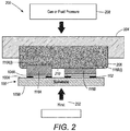
- FIGURE 2 depicted is a side view of an attachment or bonding device 200 designed to bond multiple chips of different heights in a dense configuration.
- the device 200 is being shown in use with the previously illustrated arrangement which includes the flexible substrate 100 , which has the conductive traces 102 covered by the ACA (e.g ., in certain embodiments being an ACF and/or ACP) 104 (in a tacky state 104A ) and which carries semiconductor chips of differing heights 116A , 116B .
- the arrangement is in operational arrangement with heater (e.g., a heated platen) 202 positioned adjacent the second surface 100B of the flexible substrate 100 .
- heater e.g., a heated platen
- the attachment or bonding device 200 further includes a support member 204 to which is attached a bonding head (also called herein compliant plug, of rubber or other polymer) 206 .
- a movement element (which may be in the form of an gas (e.g., air) cylinder mechanism, hydraulic mechanism, or other appropriate motivating arrangement) 208 is in operational position to move the support member 204 and therefore the bonding head 206 into association with upper surface 116A(i) of semiconductor chip 116A and an upper surface 116B(i) of semiconductor chip 116B .
- thermosetting adhesive of the ACA As the movement element 208 is activated to move the support member 204 and bonding head 206 into contact with the semiconductor chips 116A, 116B , heat from the heated platen 202 and pressure from the upper portion of the attachment or bonding device 200 apply heat and pressure, thereby curing the thermosetting adhesive of the ACA while simultaneously pressing and deforming spherical elements (conductive balls) and at substantially the same time curing of the thermosetting adhesive is taking place.
- An appropriate force factor for the movement element (i.e., in the form of an air cylinder or hydraulic cylinder) 208 allows for the use of standard levels of air pressure and/or hydraulic pressure to achieve very large forces on the semiconductor chips.
- the force factor will depend on the pressure that needs to be applied and that is proportional to the total area of the semiconductor chips being bonded.
- a typical upper level of useful air pressure is about 80 psi.
- an air cylinder with a force factor of 3 (which gives a maximum applied pressure of 240 psi) was used. This can be increased if a large number of chips are being bonded.
- a fluoropolymer film 210 is, in certain embodiments, applied to the surface of the bonding head 206 to diminish or prevent sticking of the semiconductor chips 116A , 116B to the bonding head 206 when the pressure is removed.
- the tacky ACA 104A of FIGURE 2 is shown extending across a gap between traces 102 . This is provided as one possibility if the tackiness has a sufficient stiffness. In other embodiments, the tacky ACA would encompass the semiconductor chips but not the gap area (similar concepts are also appropriate for FIGURES 3 , 4 , and 5 ).
- a particular aspect of attachment or bonding device 200 is that the bonding head 206 is compliant and allows for deformation when downward pressure is applied causing a meeting with the top surfaces 116A , 116B .
- the semiconductor chip 116A acts to deform the bonding head to a greater degree than the semiconductor chip 116B which has a lower height profile than semiconductor chip 116A .
- a neoprene rubber may be used as the bonding head (i.e., compliant plug) 206 .
- a material of 40A hardness was found to be useful for the present operation. It is understood that a softer rubber would tend to be more useful when there is a greater disparity in height of the semiconductor chips being bonded. For a large enough disparity in height there will be significant differences in the compressive force being applied to different height chips because of the difference in the amount of compression of the rubber over each chip.
- FIGURE 3 illustrated is an alternative multiple semiconductor chip attachment or bonding device 300 . While the materials on the flexible substrate 100 are similar to those discussed in connection with FIGURE 2 as well as the flexible substrate 100 being operationally associated with a heated platen 202 , the pressure providing mechanism for the top of the semiconductor chips 116A and 116B is implemented in a different manner. More particularly, support members 302A , 302B hold an expandable elastic membrane 304 which, in certain embodiments, may be, but is not limited to approximately 1/8 inch thick.
- attachment or bonding device 300 is also shown in attachment or bonding device 300 .
- a movement element 306 similar to that discussed in connection with FIGURE 2 .
- the actual implementation may be slightly different as the pressure is being applied to the expandable elastic membrane 304 rather than to a non-flexible support member or carrier (e.g., 204 of FIGURE 2 ).
- the arrangement to move the expandable elastic membrane 304 may be a gas (e.g., air) cylinder mechanism, a hydraulic mechanism, or other appropriate motivating arrangement. More particularly, this motivating force (gas pressure or fluid pressure) is directly applied to the expandable elastic membrane 304 which pushes the membrane down and causes it to conform to the profiles of the semiconductor chips to be attached or bonded. Similar to the concepts in FIGURE 2 , for the taller semiconductor chip 106a , there will be more of an impediment to the movement of the expandable elastic membrane 304 downward. However, each semiconductor chip will engage with the expandable elastic membrane 304. By this arrangement heat and pressure is thereby applied to the flexible substrate arrangement 100 resulting in an attachment or bonding of the semiconductor chips 116A and 116B .
- gas e.g., air
- hydraulic mechanism e.g., hydraulic mechanism
- FIGURE 4 illustrated is a further embodiment of an attachment or bonding device 400 .
- a flexible substrate 100 and associated elements previously discussed e.g., conductive traces 102 , tacky ACA 104A , semiconductor chips 116A , 116B
- a heated platen 202 such as in the previous embodiments is also provided.
- Distinguishing characteristics of attachment or bonding device 400 is in the use of a plurality of pins held in a support structure (e.g., a pin screen) 404 in a manner that allows the pins to move transversely back and forth, particularly when pressure is applied at ends 402A of pins 402 .
- an elastic plug 406 is provided (in certain embodiments made of a rubber or other polymer).
- a carrying mechanism 408 which is movable. As the carrying mechanism 408 moves downward towards the top surfaces of semiconductor chips 116A , 116B , the pin ends 402A come into contact with the top surfaces of the semiconductor chips 116A , 116B . This causes the pins 402 to be pushed back into the elastic plug 406 .
- the deformability and strength of the elastic plug 406 is selected such that sufficient pressure is provided on the top surface of the semiconductor chips 116A , 116B that as heat is supplied by heater (e.g., heat platen) 202 , the bonding of the chips take place in a substantially simultaneous manner, even though semiconductor chips 116A and 116B have different height profiles.
- FIGURE 5 depicted is yet another embodiment using the pin screen type structure.
- the attachment or bonding device 500 again is similarly arranged to operate with the previously discussed flexible substrate 100 , conductive traces 102 , tacky ACA 104A , and semiconductor chips 116A , 116B .
- a heated platen 202 is provided on a bottom side surface of the flexible substrate 100 .
- an elastic membrane 502 is provided which is secured at ends 504A , 504B .
- the pins 506 again arranged to be securely movable within a holding region 508 , being able to translate movement depending on pressure applied to the tips 506A of pins 506 .
- a gas e.g., air
- hydraulic or other appropriate source of pressure 510 is provided on one side of membrane 502 .
- the pressure (such as similarly discussed in connection with the previous embodiments) is applied causing the membrane to move in a downward direction, such as by arrow 512 , the pins move into contact with the upper surfaces of semiconductor chips 116A , 116B and the membrane 502 supplies the pressure to the semiconductor chips 116A , 116B such that pressure and heat are sufficient to perform the attachment or bonding process in a simultaneous manner.
- FIGURE 6A illustrated are two semiconductor chips (e.g ., resistors) having two different height components such as semiconductor chip 602 being 1.75 mm and semiconductor chip 604 being 0.6 mm. These chips have been bonded with the use of ACF to conductive traces as discussed in the previous examples. In other words, they have been bonded in a simultaneous bonding operation even though they have significant different height components.
- semiconductor chip 602 being 1.75 mm
- semiconductor chip 604 being 0.6 mm.
- These chips have been bonded with the use of ACF to conductive traces as discussed in the previous examples. In other words, they have been bonded in a simultaneous bonding operation even though they have significant different height components.
- FIGURE 6B illustrates two resistors 610 , 612 bound side-by-side in a high density close proximity configuration using the concepts of the present application. It is understood that the present application teaches methods and processed as well as systems and devices that allow for a substantially simultaneous bonding for attachment of semiconductor chips having intentionally different distinct height profiles. This is an aspect which is particularly suitable for packing of hybrid electronics on flexible substrates.
Landscapes
- Wire Bonding (AREA)
- Electric Connection Of Electric Components To Printed Circuits (AREA)
- Adhesives Or Adhesive Processes (AREA)
- Engineering & Computer Science (AREA)
- Manufacturing & Machinery (AREA)
Priority Applications (1)
| Application Number | Priority Date | Filing Date | Title |
|---|---|---|---|
| EP19213869.1A EP3657539A1 (de) | 2016-10-24 | 2017-10-19 | Verfahren und vorrichtung zur gleichzeitigen verbindung mehrerer chips von unterschiedlicher höhe auf einem flexiblen substrat mittels eines anisotropen leitfähigen films oder einer anisotropen leitfähigen paste |
Applications Claiming Priority (1)
| Application Number | Priority Date | Filing Date | Title |
|---|---|---|---|
| US15/332,326 US10147702B2 (en) | 2016-10-24 | 2016-10-24 | Method for simultaneously bonding multiple chips of different heights on flexible substrates using anisotropic conductive film or paste |
Related Child Applications (1)
| Application Number | Title | Priority Date | Filing Date |
|---|---|---|---|
| EP19213869.1A Division EP3657539A1 (de) | 2016-10-24 | 2017-10-19 | Verfahren und vorrichtung zur gleichzeitigen verbindung mehrerer chips von unterschiedlicher höhe auf einem flexiblen substrat mittels eines anisotropen leitfähigen films oder einer anisotropen leitfähigen paste |
Publications (2)
| Publication Number | Publication Date |
|---|---|
| EP3312877A2 true EP3312877A2 (de) | 2018-04-25 |
| EP3312877A3 EP3312877A3 (de) | 2018-08-08 |
Family
ID=60164608
Family Applications (2)
| Application Number | Title | Priority Date | Filing Date |
|---|---|---|---|
| EP19213869.1A Withdrawn EP3657539A1 (de) | 2016-10-24 | 2017-10-19 | Verfahren und vorrichtung zur gleichzeitigen verbindung mehrerer chips von unterschiedlicher höhe auf einem flexiblen substrat mittels eines anisotropen leitfähigen films oder einer anisotropen leitfähigen paste |
| EP17197418.1A Ceased EP3312877A3 (de) | 2016-10-24 | 2017-10-19 | Verfahren und vorrichtung zur gleichzeitigen verbindung mehrerer chips von unterschiedlicher höhe auf einem flexiblen substrat mittels eines anisotropen leitfähigen films oder einer anisotropen leitfähigen paste |
Family Applications Before (1)
| Application Number | Title | Priority Date | Filing Date |
|---|---|---|---|
| EP19213869.1A Withdrawn EP3657539A1 (de) | 2016-10-24 | 2017-10-19 | Verfahren und vorrichtung zur gleichzeitigen verbindung mehrerer chips von unterschiedlicher höhe auf einem flexiblen substrat mittels eines anisotropen leitfähigen films oder einer anisotropen leitfähigen paste |
Country Status (3)
| Country | Link |
|---|---|
| US (1) | US10147702B2 (de) |
| EP (2) | EP3657539A1 (de) |
| JP (1) | JP6931311B2 (de) |
Cited By (2)
| Publication number | Priority date | Publication date | Assignee | Title |
|---|---|---|---|---|
| US20220122939A1 (en) * | 2020-10-15 | 2022-04-21 | Gallant Micro. Machining Co., Ltd. | Producing apparatus and pre-bonding device |
| WO2023061872A3 (de) * | 2021-10-14 | 2023-09-07 | Pink Gmbh Thermosysteme | Multifunktionale sinter- oder diffusionslötvorrichtung und presswerkzeug |
Families Citing this family (4)
| Publication number | Priority date | Publication date | Assignee | Title |
|---|---|---|---|---|
| DE102015120156B4 (de) * | 2015-11-20 | 2019-07-04 | Semikron Elektronik Gmbh & Co. Kg | Vorrichtung zur materialschlüssigen Verbindung von Verbindungspartnern eines Leistungselekronik-Bauteils und Verwendung einer solchen Vorrichtung |
| JP2020119983A (ja) * | 2019-01-23 | 2020-08-06 | トヨタ自動車株式会社 | 半導体素子接合装置、及び半導体素子接合方法 |
| KR102789194B1 (ko) * | 2020-05-12 | 2025-03-28 | 삼성전자주식회사 | 반도체 칩 실장용 테이프 및 상기 테이프를 이용한 반도체 패키지 제조 방법 |
| KR102949513B1 (ko) * | 2023-05-15 | 2026-04-09 | 코스텍시스템(주) | 칩 접합 장비와 이를 포함하는 칩 접합 시스템 및 그 접합 방법 |
Family Cites Families (16)
| Publication number | Priority date | Publication date | Assignee | Title |
|---|---|---|---|---|
| US5353498A (en) * | 1993-02-08 | 1994-10-11 | General Electric Company | Method for fabricating an integrated circuit module |
| US5861678A (en) * | 1997-12-23 | 1999-01-19 | Micron Technology, Inc. | Method and system for attaching semiconductor dice to substrates |
| JP2000150560A (ja) * | 1998-11-13 | 2000-05-30 | Seiko Epson Corp | バンプ形成方法及びバンプ形成用ボンディングツール、半導体ウエーハ、半導体チップ及び半導体装置並びにこれらの製造方法、回路基板並びに電子機器 |
| EP1156520A4 (de) * | 1999-01-29 | 2004-08-25 | Matsushita Electric Industrial Co Ltd | Bestückungsverfahren für elektronische bauteile und dessen vorrichtung |
| JP2002110744A (ja) * | 2000-09-26 | 2002-04-12 | Matsushita Electric Ind Co Ltd | 半導体実装装置、および半導体実装方法 |
| JP2002198395A (ja) * | 2000-12-26 | 2002-07-12 | Seiko Epson Corp | 半導体装置及びその製造方法、回路基板並びに電子機器 |
| JP4710205B2 (ja) | 2001-09-06 | 2011-06-29 | ソニー株式会社 | フリップチップ実装方法 |
| KR100604334B1 (ko) * | 2003-11-25 | 2006-08-08 | (주)케이나인 | 플립칩 패키징 공정에서 접합력이 향상된 플립칩 접합 방법 |
| US20050282355A1 (en) * | 2004-06-18 | 2005-12-22 | Edwards David N | High density bonding of electrical devices |
| JP4925669B2 (ja) | 2006-01-13 | 2012-05-09 | ソニーケミカル&インフォメーションデバイス株式会社 | 圧着装置及び実装方法 |
| JP2007294607A (ja) * | 2006-04-24 | 2007-11-08 | Sony Chemical & Information Device Corp | 押圧ヘッド及び押圧装置 |
| KR100785493B1 (ko) * | 2006-05-04 | 2007-12-13 | 한국과학기술원 | 접착제의 수분흡습을 방지하는 플립칩용 웨이퍼 레벨패키지 제조방법 |
| US7884719B2 (en) * | 2006-11-21 | 2011-02-08 | Rcd Technology Inc. | Radio frequency identification (RFID) tag lamination process |
| RU2490837C2 (ru) * | 2009-03-26 | 2013-08-20 | Шарп Кабусики Кайся | Способ монтажа микроэлектронных компонентов |
| US8520399B2 (en) * | 2010-10-29 | 2013-08-27 | Palo Alto Research Center Incorporated | Stretchable electronics modules and circuits |
| JP2013084790A (ja) * | 2011-10-11 | 2013-05-09 | Sharp Corp | 熱圧着装置 |
-
2016
- 2016-10-24 US US15/332,326 patent/US10147702B2/en active Active
-
2017
- 2017-10-04 JP JP2017193915A patent/JP6931311B2/ja not_active Expired - Fee Related
- 2017-10-19 EP EP19213869.1A patent/EP3657539A1/de not_active Withdrawn
- 2017-10-19 EP EP17197418.1A patent/EP3312877A3/de not_active Ceased
Non-Patent Citations (1)
| Title |
|---|
| None |
Cited By (5)
| Publication number | Priority date | Publication date | Assignee | Title |
|---|---|---|---|---|
| US20220122939A1 (en) * | 2020-10-15 | 2022-04-21 | Gallant Micro. Machining Co., Ltd. | Producing apparatus and pre-bonding device |
| US11784158B2 (en) * | 2020-10-15 | 2023-10-10 | Gallant Micro. Machining Co., Ltd. | Producing apparatus |
| WO2023061872A3 (de) * | 2021-10-14 | 2023-09-07 | Pink Gmbh Thermosysteme | Multifunktionale sinter- oder diffusionslötvorrichtung und presswerkzeug |
| CN118103967A (zh) * | 2021-10-14 | 2024-05-28 | 平克塞莫系统有限公司 | 多功能烧结或扩散焊接设备和冲压工具 |
| US12121987B1 (en) | 2021-10-14 | 2024-10-22 | Pink Gmbh Thermosysteme | Multifunctional sintering or diffusion soldering device and pressing tool |
Also Published As
| Publication number | Publication date |
|---|---|
| JP6931311B2 (ja) | 2021-09-01 |
| US10147702B2 (en) | 2018-12-04 |
| EP3657539A1 (de) | 2020-05-27 |
| JP2018074148A (ja) | 2018-05-10 |
| EP3312877A3 (de) | 2018-08-08 |
| US20180114772A1 (en) | 2018-04-26 |
Similar Documents
| Publication | Publication Date | Title |
|---|---|---|
| EP3312877A2 (de) | Verfahren und vorrichtung zur gleichzeitigen verbindung mehrerer chips von unterschiedlicher höhe auf einem flexiblen substrat mittels eines anisotropen leitfähigen films oder einer anisotropen leitfähigen paste | |
| KR20200019133A (ko) | 표시 장치의 제조 방법, 칩 부품의 전사 방법, 및 전사 부재 | |
| CN107210239B (zh) | 安装装置和安装方法 | |
| US20120018084A1 (en) | Printed Circuit Board Assembly Manufacturing Device And Method | |
| TWI664681B (zh) | 安裝用頭及使用其之安裝裝置 | |
| TWI681478B (zh) | 安裝裝置及安裝方法 | |
| KR102403569B1 (ko) | 열압착 본더, 열압착 본더 작동 방법, 및 미세 피치의 플립 칩 조립체 상호 접속 방법 | |
| KR0179717B1 (ko) | 반도체 패키지의 제조방법과 반도체의 실장방법 및 반도체 실장장치 | |
| JP6234277B2 (ja) | 圧着ヘッド、それを用いた実装装置および実装方法 | |
| JP2018074148A5 (de) | ||
| KR20030012808A (ko) | 반도체 실장체 제조 방법 및 장치 | |
| KR102468101B1 (ko) | 소자 실장 장치 | |
| US8286340B2 (en) | Method of manufacturing and warpage correcting of printed circuit board assembly | |
| US20230093241A1 (en) | Element array pressurizing device, manufacturing device, and manufacturing method | |
| US6559523B2 (en) | Device for attaching a semiconductor chip to a chip carrier | |
| CN115668468B (zh) | 接合装置以及接合头调整方法 | |
| JPH08293525A (ja) | リード付き基板の接合方法 | |
| JP6385885B2 (ja) | ボンディング装置 | |
| CN110199587B (zh) | 电子元件安装用装置 | |
| JP2021141158A (ja) | 素子アレイの加圧装置、製造装置および製造方法 | |
| JP6752722B2 (ja) | 実装装置および実装方法 | |
| KR102284943B1 (ko) | 본딩 장치 및 본딩 방법 | |
| KR20220150827A (ko) | 반도체 디바이스를 접합하기 위한 가요성 소결 도구 | |
| JP2004259917A (ja) | ボンディング方法および装置 | |
| JP2021141160A (ja) | 素子アレイの加圧装置、製造装置および製造方法 |
Legal Events
| Date | Code | Title | Description |
|---|---|---|---|
| PUAI | Public reference made under article 153(3) epc to a published international application that has entered the european phase |
Free format text: ORIGINAL CODE: 0009012 |
|
| STAA | Information on the status of an ep patent application or granted ep patent |
Free format text: STATUS: THE APPLICATION HAS BEEN PUBLISHED |
|
| AK | Designated contracting states |
Kind code of ref document: A2 Designated state(s): AL AT BE BG CH CY CZ DE DK EE ES FI FR GB GR HR HU IE IS IT LI LT LU LV MC MK MT NL NO PL PT RO RS SE SI SK SM TR |
|
| AX | Request for extension of the european patent |
Extension state: BA ME |
|
| PUAL | Search report despatched |
Free format text: ORIGINAL CODE: 0009013 |
|
| AK | Designated contracting states |
Kind code of ref document: A3 Designated state(s): AL AT BE BG CH CY CZ DE DK EE ES FI FR GB GR HR HU IE IS IT LI LT LU LV MC MK MT NL NO PL PT RO RS SE SI SK SM TR |
|
| AX | Request for extension of the european patent |
Extension state: BA ME |
|
| RIC1 | Information provided on ipc code assigned before grant |
Ipc: H01L 21/98 20060101AFI20180629BHEP Ipc: H01L 21/67 20060101ALI20180629BHEP Ipc: H01L 21/60 20060101ALI20180629BHEP |
|
| STAA | Information on the status of an ep patent application or granted ep patent |
Free format text: STATUS: REQUEST FOR EXAMINATION WAS MADE |
|
| STAA | Information on the status of an ep patent application or granted ep patent |
Free format text: STATUS: EXAMINATION IS IN PROGRESS |
|
| 17P | Request for examination filed |
Effective date: 20190208 |
|
| RBV | Designated contracting states (corrected) |
Designated state(s): AL AT BE BG CH CY CZ DE DK EE ES FI FR GB GR HR HU IE IS IT LI LT LU LV MC MK MT NL NO PL PT RO RS SE SI SK SM TR |
|
| 17Q | First examination report despatched |
Effective date: 20190318 |
|
| STAA | Information on the status of an ep patent application or granted ep patent |
Free format text: STATUS: THE APPLICATION HAS BEEN REFUSED |
|
| 18R | Application refused |
Effective date: 20191226 |