EP3316295B1 - Vorrichtung mit einem stapel elektronischer chips - Google Patents
Vorrichtung mit einem stapel elektronischer chips Download PDFInfo
- Publication number
- EP3316295B1 EP3316295B1 EP17164858.7A EP17164858A EP3316295B1 EP 3316295 B1 EP3316295 B1 EP 3316295B1 EP 17164858 A EP17164858 A EP 17164858A EP 3316295 B1 EP3316295 B1 EP 3316295B1
- Authority
- EP
- European Patent Office
- Prior art keywords
- chip
- loop
- track
- vias
- circuit
- Prior art date
- Legal status (The legal status is an assumption and is not a legal conclusion. Google has not performed a legal analysis and makes no representation as to the accuracy of the status listed.)
- Active
Links
Images



Classifications
-
- H—ELECTRICITY
- H10—SEMICONDUCTOR DEVICES; ELECTRIC SOLID-STATE DEVICES NOT OTHERWISE PROVIDED FOR
- H10W—GENERIC PACKAGES, INTERCONNECTIONS, CONNECTORS OR OTHER CONSTRUCTIONAL DETAILS OF DEVICES COVERED BY CLASS H10
- H10W42/00—Arrangements for protection of devices
- H10W42/40—Arrangements for protection of devices protecting against tampering, e.g. unauthorised inspection or reverse engineering
- H10W42/405—Arrangements for protection of devices protecting against tampering, e.g. unauthorised inspection or reverse engineering using active circuits
-
- H—ELECTRICITY
- H10—SEMICONDUCTOR DEVICES; ELECTRIC SOLID-STATE DEVICES NOT OTHERWISE PROVIDED FOR
- H10W—GENERIC PACKAGES, INTERCONNECTIONS, CONNECTORS OR OTHER CONSTRUCTIONAL DETAILS OF DEVICES COVERED BY CLASS H10
- H10W20/00—Interconnections in chips, wafers or substrates
- H10W20/20—Interconnections within wafers or substrates, e.g. through-silicon vias [TSV]
-
- H—ELECTRICITY
- H10—SEMICONDUCTOR DEVICES; ELECTRIC SOLID-STATE DEVICES NOT OTHERWISE PROVIDED FOR
- H10W—GENERIC PACKAGES, INTERCONNECTIONS, CONNECTORS OR OTHER CONSTRUCTIONAL DETAILS OF DEVICES COVERED BY CLASS H10
- H10W90/00—Package configurations
-
- H—ELECTRICITY
- H10—SEMICONDUCTOR DEVICES; ELECTRIC SOLID-STATE DEVICES NOT OTHERWISE PROVIDED FOR
- H10W—GENERIC PACKAGES, INTERCONNECTIONS, CONNECTORS OR OTHER CONSTRUCTIONAL DETAILS OF DEVICES COVERED BY CLASS H10
- H10W70/00—Package substrates; Interposers; Redistribution layers [RDL]
- H10W70/60—Insulating or insulated package substrates; Interposers; Redistribution layers
- H10W70/62—Insulating or insulated package substrates; Interposers; Redistribution layers characterised by their interconnections
- H10W70/63—Vias, e.g. via plugs
-
- H—ELECTRICITY
- H10—SEMICONDUCTOR DEVICES; ELECTRIC SOLID-STATE DEVICES NOT OTHERWISE PROVIDED FOR
- H10W—GENERIC PACKAGES, INTERCONNECTIONS, CONNECTORS OR OTHER CONSTRUCTIONAL DETAILS OF DEVICES COVERED BY CLASS H10
- H10W72/00—Interconnections or connectors in packages
- H10W72/01—Manufacture or treatment
-
- H—ELECTRICITY
- H10—SEMICONDUCTOR DEVICES; ELECTRIC SOLID-STATE DEVICES NOT OTHERWISE PROVIDED FOR
- H10W—GENERIC PACKAGES, INTERCONNECTIONS, CONNECTORS OR OTHER CONSTRUCTIONAL DETAILS OF DEVICES COVERED BY CLASS H10
- H10W90/00—Package configurations
- H10W90/20—Configurations of stacked chips
- H10W90/26—Configurations of stacked chips the stacked chips being of the same size without any chips being laterally offset, e.g. chip stacks having a rectangular shape
-
- H—ELECTRICITY
- H10—SEMICONDUCTOR DEVICES; ELECTRIC SOLID-STATE DEVICES NOT OTHERWISE PROVIDED FOR
- H10W—GENERIC PACKAGES, INTERCONNECTIONS, CONNECTORS OR OTHER CONSTRUCTIONAL DETAILS OF DEVICES COVERED BY CLASS H10
- H10W90/00—Package configurations
- H10W90/20—Configurations of stacked chips
- H10W90/297—Configurations of stacked chips characterised by the through-semiconductor vias [TSVs] in the stacked chips
-
- H—ELECTRICITY
- H10—SEMICONDUCTOR DEVICES; ELECTRIC SOLID-STATE DEVICES NOT OTHERWISE PROVIDED FOR
- H10W—GENERIC PACKAGES, INTERCONNECTIONS, CONNECTORS OR OTHER CONSTRUCTIONAL DETAILS OF DEVICES COVERED BY CLASS H10
- H10W90/00—Package configurations
- H10W90/701—Package configurations characterised by the relative positions of pads or connectors relative to package parts
- H10W90/721—Package configurations characterised by the relative positions of pads or connectors relative to package parts of bump connectors
- H10W90/722—Package configurations characterised by the relative positions of pads or connectors relative to package parts of bump connectors between stacked chips
-
- H—ELECTRICITY
- H10—SEMICONDUCTOR DEVICES; ELECTRIC SOLID-STATE DEVICES NOT OTHERWISE PROVIDED FOR
- H10W—GENERIC PACKAGES, INTERCONNECTIONS, CONNECTORS OR OTHER CONSTRUCTIONAL DETAILS OF DEVICES COVERED BY CLASS H10
- H10W90/00—Package configurations
- H10W90/701—Package configurations characterised by the relative positions of pads or connectors relative to package parts
- H10W90/721—Package configurations characterised by the relative positions of pads or connectors relative to package parts of bump connectors
- H10W90/724—Package configurations characterised by the relative positions of pads or connectors relative to package parts of bump connectors between a chip and a stacked insulating package substrate, interposer or RDL
Definitions
- the present application relates to the field of electronic chips, and relates in particular to a device comprising a stack of interconnected electronic chips.
- Some electronic chips such as bank card chips can contain confidential data that may be renowned by hackers. These confidential data can be contained in circuits located on the side of the front face of the chip. To obtain this data, a hacker can carry out an attack from the back side of the chip.
- an etching attack In one type of attack, called an etching attack, the hacker etches part of the back face of the chip. From this engraved part, the pirate engraves cavities a few micrometers wide, for example using an ion beam, which extend towards the front face up to the level of the circuits. Electrical contacts with circuit elements are then created in these cavities, and the hacker uses these contacts to analyze the chip in operation.
- the pirate for example scans the rear face of the chip with laser pulses.
- the impact of the laser disrupts the functioning of the chip. It is the observation of the consequences of these disturbances on the activity of the circuits that allows the pirate to carry out his attack.
- the hacker can also apply positive or negative potentials by means of a probe in contact with the rear face, or induce currents or voltages in the elements of the circuits by means of a coil arranged near the back side.
- This type of attack is called a fault injection attack.
- Such a chip comprising confidential data can be included in a stack of interconnected chips.
- the document US2003 / 008432 describes a method and a device for securing a stack of chips and a configuration of chips made in a multidimensional manner.
- the document WO2011 / 155114 describes a protection circuit, a semiconductor device and electronic equipment.
- the invention provides a device as defined in claim 1.
- Preferred embodiments are defined in the dependent claims. Examples of the present description not covered by the claims do not form part of the invention.
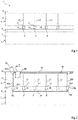
- the figure 1 is a schematic sectional view illustrating an example of a device 1 comprising a stack of chips electronic.
- the device 1 comprises a chip 3, and a chip 5 located above the chip 3.
- the chips 3 and 5 each have a front face in the upper part and a rear face in the lower part. Chip 3 is thus located on the back side of chip 5.
- the chip 3 comprises a semiconductor substrate 7.
- the substrate 7 comprises, on the side of its upper face (or front face), semiconductor elements of components such as transistors or diodes of circuits not shown.
- the chip 3 further comprises an interconnection layer 8 covering the substrate 7 on the side of its upper face.
- the interconnection layer 8 contains, within insulating layers, conductive tracks, not shown, which connect the components of the circuits of the chip 3.
- the chip 3 comprises, on the upper face of the interconnection layer 8, connection pads 9 electrically connected to the circuits of chip 3 by tracks of layer 8.
- the chip 5 comprises a semiconductor substrate 13.
- the chip 5 comprises circuits located on the side of its front face, these circuits comprising components formed in and on the substrate 13 on the side of the upper face of the substrate 13.
- the chip 5 comprises a interconnection layer 14 covering the substrate 13 on the side of its upper face (or front face).
- the interconnection layer 14 contains, within insulating layers, conductive tracks, not shown, which connect the components of the circuits of the chip 5.
- the chip 5 further comprises through vias 15.
- through through is used. Here is understood to mean a conductive through via passing entirely right through the substrate 13, from the upper face of the substrate to the lower face (or rear face) of the substrate.
- the vias 15 each have, on the front face side, one end connected to the circuits of the chip 5 by tracks of the layer 14, and, on the rear face side, one end connected to a connection pad 17 located on the rear face of the chip. upper 5.
- Each connection pad 17 of the upper chip 5 is soldered to a connection pad 9 of the chip lower 3.
- a filler material 18 can be provided between the pads 9 and 17 to perform the brazing. Connections are thus obtained between the circuits of chip 3 and those of chip 5.
- the circuits of the upper chip 5 contain confidential data wished by a hacker.
- the hacker cannot attack the rear side of the chip 5.
- the hacker must therefore start by separating the pads 9 and 17 in order to remove chip 3 and access the back side of chip 5.
- the hacker can then conduct his attack from the back side of chip 5.
- the hacker connects chip 5 to a source of power supply to put it into operation.
- the hacker can also electrically reconnect the pads 9 and 17 by conductive wires, so as to re-establish the electrical connection between the two chips while maintaining access to the rear face of the chip 5.
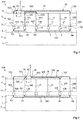
- the figure 2 is a schematic sectional view of an example of a device comprising a stack of electronic chips.
- the device 20 comprises the same elements as the device 1 of the figure 1 , arranged substantially in the same way. The common elements between the two devices will not be detailed again below.
- the upper chip 5 of the device 20 comprises two additional through-conductor vias 30A and 30B.
- Each of the vias 30A and 30B has one end, respectively 32A, 32B, located on the side of the front face of the chip 5, and another end, respectively 34A, 34B, located on the side of the rear face of the chip 5.
- the upper ends 32A and 32B of vias 30A and 30B are electrically connected to each other by a conductive track 36 located in the interconnection layer 14 of chip 5.
- the lower ends 34A and 34B of vias 30A and 30B are electrically connected to each other by a conductive track 38 located in the interconnection layer 8 of the lower chip 3.
- the upper chip 5 comprises two additional connection pads 17A and 17B located on the rear face of the upper chip 5 and connected respectively to the ends 34A and 34B of the vias 30A and 30B.
- the lower chip 3 comprises two additional connection pads 9A and 9B located on the front face of the chip 3 and connected respectively to a first and a second end of the track 38, the pads 17A and 17B being soldered respectively to the pads 9A and 9B.
- the device thus comprises a conductive loop 39 comprising the through vias 30A and 30B connected in series by the tracks 36 and 38.
- the upper chip 5 further comprises a detection circuit 40 configured to monitor an electrical characteristic of the loop 39, for example an absence of electrical continuity of the loop 39.
- the chip 5 of the device 20 is thus protected against attacks by its rear face.
- the lower chip 3 has lateral dimensions greater than or equal to those of the upper chip 5 and the whole of the rear face of the chip 5 is opposite the chip 3..
- the chip 3 is located opposite only part of the rear face of the chip 5, corresponding to the sensitive circuits to be protected on the chip 5.
- the detection circuit 40 is placed in series with a conductive portion of the loop 39 of which it is desired to detect an electrical characteristic.
- the circuit 40 is included in the loop 39.
- the detection circuit 40 is located between nodes 42 and 44 located on the track 36 so as to interrupt the track 36.
- the detection circuit is located between track 36 and the end 32A of via 30A or between track 36 and the end 32B of via 30B.
- the detection circuit 40 is then configured to detect an electrical characteristic of the conductive portion of the loop 39 located outside the detection circuit 40.
- the detection circuit 40 can be adapted to monitor one or more other electrical characteristics of loop 39, for example to compare the value of the electrical resistance of loop 39 between nodes 42 and 44 with a reference value, or to compare at a reference duration the time taken by an electric pulse emitted by circuit 40 to travel through the loop.
- One advantage of these alternatives is that they make it possible to detect that the chips 3 and 5 have been reconnected by conductive wires after having been disconnected, which cannot be detected by a simple check of the electrical continuity of the loop 39.
- the figure 3 is a perspective diagram illustrating in more detail an embodiment of the loop 39 of the device of the figure 2 . Only tracks 36 and 38, vias 30A and 30B and circuit 40 have been shown on the figure 3 . The interconnection layers 8 and 14 have been shown schematically by two parallel planes.
- the track 36 of the upper chip 5 has in top view the shape of a coil arranged in a plane substantially parallel to the upper face of the chip.
- the coil can be arranged at a metallization level of the chip located above that of the interconnection tracks of the circuits of the chip.
- the sensitive circuits to be protected of the chip 5 are arranged in part or in whole in a zone of the chip in which, in top view, the serpentine pattern extends.
- the sensitive circuits are arranged in part or in whole in an area of the chip, each point of which is situated in top view between two portions of the track 36 separated by a distance of less than 5 ⁇ m, preferably less than 2 pm.
- An advantage of this arrangement of the track 36 is that it also makes it possible to protect the chip 5 against a possible attack from its front face. Indeed, if a hacker tried to access the components of the sensitive circuits of the chip 5 through the interconnection layer 14, he would inevitably interrupt the track 36, and the circuit 40 would detect the attack.
- the upper chip 5 is thus advantageously protected by a single circuit 40 both against attacks from its front face and against attacks from its rear face. The protection of the upper chip 5 is thus obtained by a particularly small number of components.
- the track 38 of the lower chip 3 also has in top view the shape of a coil, for example identical or similar to the coil shape of the track 36.
- the sensitive circuits of chip 5 are in part or in whole arranged opposite a zone of chip 3 in which the serpentine pattern of track 38 extends with a view to above.
- the hacker To access the components of the sensitive circuits of chip 5 through its rear face, the hacker must remove from chip 3 a portion whose lateral dimensions are greater than those of the accesses to the components that the hacker would achieve if he wanted to attack the chip. chip 5 by its front face.
- the coil 38 can be less constricted than the coil 36, for example the sensitive circuits of the chip 5 are partly or entirely arranged in a zone, each point of which situated in top view between two portions of the track 38 separated from each other. 'a distance of less than 50 ⁇ m, preferably less than 20 ⁇ m.
- the coil 38 and the coil 36 are similar, the sensitive circuits of the chip 5 being in part or in whole arranged in an area of which each point is situated in top view between two portions of the track 38 separated from it. 'a distance of less than 5 ⁇ m, preferably less than 2 ⁇ m.
- the figure 4 is a schematic sectional view of an alternative embodiment of the device 20 of the figure 2 .
- the figure 4 illustrates more particularly a device 20A comprising elements similar to those of the device 20 of the figure 2 , arranged in a similar manner.
- the elements common to the two devices will not be described again below. In the following, only the differences between the devices 20A and 20 will be highlighted.
- the loop 39 comprises additional through-conductive vias 30C and 30D located in the chip 5.
- the vias 30C and 30D each have one end, respectively 32C and 32D, on the front side of the chip 5, and the other end, respectively 34C and 34D, rear face side of the chip 5.
- the ends 32C and 32D of the vias 30C and 30D are connected by an additional track 36A located in the interconnection layer 14 of the chip 5.
- the ends 34C and 34D are connected to additional connection pads, respectively 17C and 17D, located on the rear face of chip 5.
- Track 38 of chip 3 has been replaced by tracks 38A and 38B located in interconnection layer 8.
- chip 3 includes additional connection pads 9C and 9D located on the front face of chip 3.
- Track 38A connects connection pad 9A to connection pad 9C
- track 38B connects connection pad 9B to connection pad 9D.
- the pads 9C and 9D are soldered to the pads 17C and 17D respectively.
- the loop 39 of the device 20A thus comprises the four vias 30A, 30B, 30C, 30D connected in series by the tracks 36, 36A, 38A, 38B.
- the tracks 36, 36A, 38A, 38B are located alternately in the upper chip 5 and in the lower chip 3.
- the portion of the loop 39 for which one seeks to monitor an electrical characteristic passes alternately through chip 5 and through chip 3 a plurality of times.
- chip 5 comprises four through vias 30A, 30B, 30C, 30D arranged in chip 5, other examples are possible in which loop 39 comprises an even number greater than four of connected vias. in series by tracks located alternately in the upper chip 5 and in the lower chip 3.
- An advantage of the example of figure 4 is that it makes it possible to strengthen the protection of the chip 5 against attacks. Indeed, as indicated above, a hacker coveting the confidential data of the upper chip 5 could, after having disconnected the chips 3 and 5, attempt to reconnect them, for example by conducting wires, so as to keep the electrical connection. between the two chips while preserving access to the rear face of the upper chip 5. In doing so, it would re-establish the electrical continuity of the loop 39, which could prevent the detection of the attack by the circuit 40. However, this reconnection is all the more difficult as the number of vias to reconnect is high.
- the device 20A of the figure 4 thus presents a reinforced level of protection compared to the device 20 of the figure 2 .
- the figure 5 is a schematic sectional view of another variant embodiment of the device 20 of the figure 2 .
- This variant shown in figure 5 corresponds to the claimed invention.
- the figure 5 illustrates more particularly a device 20B comprising elements similar to those of the device 20 of the figure 2 , arranged in a similar manner.
- the elements common to the devices 20 and 20B will not be described again below. In the following, only the differences between the devices 20 and 20B will be highlighted.
- the device 20B comprises an additional loop 39A comprising two additional through vias 30E and 30F conductors included in the upper chip 5.
- the vias 30E and 30F have, on the front side, respective ends 32E and 32F and, on the rear side, respective ends. 34E and 34F.
- the ends 34E and 34F are connected to additional connection pads, respectively 17E and 17F, located on the rear face of the chip 5.
- the loop 39A further comprises an additional track 36B, located in the interconnection layer 14 of the chip. upper chip 5 and connecting the ends 32E and 32F of vias 30E and 30F.
- the loop 39A further comprises a track 38C included in the interconnection layer 8 of the lower chip 3.
- the track 38C interconnects additional connection pads 9E and 9F arranged on the front face of the chip 3 and respectively soldered to the ends. studs 17E and 17F.
- the loop 39A of the device 20B therefore comprises, connected in series and in the following order, in the upper chip 5, the via 30E, the track 36B and the via 30F, and, in the lower chip 3, the track 38C.
- the detection circuit 40 is placed not only in series with a conductive portion of the loop 39, as described above, but also in series with a conductive portion of the loop 39A. In other words, the circuit 40 is included in the loop 39A.
- the detection circuit 40 is located between nodes 42A and 44A located on track 36B so as to interrupt track 36B.
- the detection circuit is located between track 36B and the end 32E of via 30E or between track 36B and the end 32F of via 30F.
- the detection circuit 40 is then configured to detect an electrical characteristic of the conductive portion of the loop 39A located outside the detection circuit 40.
- the detection circuit 40 of the device 20B is configured to detect an electrical characteristic of the set of the two loops 39 and 39A. According to the invention, the presence of an electrical connection between the loops 39 and 39A is detected, or else a difference between the electrical resistance of the loop 39 between the nodes 42 and 44 and the electrical resistance of the loop 39A between the nodes 42A and 44B.
- An advantage of the embodiment of the figure 5 is that it makes it possible to strengthen the protection of the chip 5 against attacks. Indeed, if a hacker coveting the confidential data of the upper chip 5, after having disconnected the chips 3 and 5, tries to reconnect them, for example by conducting wires, he may have to create an electrical connection between the loops, such as a short circuit, or to cause a difference between the electrical resistances of the loops. This is detected by circuit 40 when the hacker puts chip 5 back into operation to continue his attack.
- the figure 6 is a schematic sectional view of another example useful for understanding the invention. This example constitutes an alternative embodiment of the device 20 of the figure 2 .
- the figure 6 illustrates more particularly a device 20C comprising elements similar to those of the device 20 of the figure 2 .
- the elements common to the two devices will not be described again below. In the following, only the differences between the devices 20C and 20 will be highlighted.
- the device 20C differs from the device 20 of the figure 2 essentially in that, in the device 20C, the lower chip 3 has its rear face turned towards the rear face of the upper chip 5.
- the front face of the chip 3 corresponds to its lower face
- the rear face of chip 3 corresponds to its upper face.
- connection pads 9 of the chip 3 have been replaced by connection pads 17 'located on its rear face.
- the pads 17 ' are connected to the circuits of the lower chip 3 by through conductive vias 15'.
- the connection pads 17 'of the lower chip 3 are soldered to the connection pads 17 of the upper chip 5.
- Chip 3 further comprises two through vias conductors 30A 'and 30B'.
- the through vias 30A 'and 30B' pass right through the substrate 7 between its upper face and its lower face.
- the through vias 30A 'and 30B' have, on the front face side of the chip 3, respective ends 32A 'and 32B', and, on the rear face side of the chip 3, respective ends 34A 'and 34B'.
- the ends 32A 'and 32B' are connected to each other by an additional track 38D located in the interconnection layer 8 of the lower chip 3.
- the ends 34A 'and 34B' of the vias 30A 'and 30B' are connected to pads.
- additional connection 17A 'and 17B' located on the rear face of the lower chip 3.
- the pads 17A 'and 17B' of the lower chip 3 are soldered respectively to the pads 17A and 17B of the upper chip 5.
- the device 20C thus comprises a loop 39 comprising in series and in the following order, in chip 5, the via 30A, track 36 and via 30B, and, in chip 3, via 30B ', track 38D and via 30A'.
- the lower chip 3 further comprises an additional detection circuit 60 suitable for monitoring an electrical characteristic of the loop 39.
- the circuit 60 is for example identical or similar to the circuit 40.
- the detection circuit 60 is placed in series with a conductive portion of the loop 39 of which it is desired to detect an electrical characteristic.
- circuit 60 is included in loop 39.
- detection circuit 60 is located between nodes 62 and 64 located on track 38D so as to interrupt track 38D.
- the detection circuit is located between track 38D and end 32A 'of via 30A' or between track 38D and end 32B 'of via 30B'.
- the detection circuit 40 comprises a bypass switch 66 coupling the nodes 42 and 44, making it possible to connect the nodes 42 and 44 in order to ensure the electrical continuity of the loop 39 inside the circuit 40
- detection circuit 60 may include a bypass switch 68 coupling nodes 62 and 64, enabling nodes 62 and 64 to be connected to ensure electrical continuity of loop 39 within circuit 60.
- Each of the detection circuits 40 and 60 can have a detection phase during which the detection circuit controls its bypass switch, respectively 66 and 68, in the non-conducting state, and monitors an electrical characteristic of the part of the circuit. loop 39 located outside the detection circuit.
- Circuits 40 and 60 are then configured so that bypass switch 66 of circuit 40 is in the on state during the detection phase of circuit 60, and so that bypass switch 68 of circuit 60 is on. on state during the detection phase of the circuit 40, the detection phases of circuits 40 and 60 being separate.
- the presence of the upper chip 5 on the side of the rear face of the lower chip 3 prevents a hacker from accessing the rear face of the chip 3 to carry out an attack on the chip 3, and the presence of the lower chip 3 on the back side of the upper chip 5 prevents a hacker from accessing the back side of the chip 5 to attack the chip 5.
- the loop 39 is intact, and none of the circuitry. detection 40 and 60 does not detect an attack.
- the hacker During an attack attempt aimed at obtaining confidential data present in the lower chip 3, the hacker removes the upper chip 5 to access the rear face of the lower chip 3. The hacker then tries to make the chip 3 work.
- the loop 39 being interrupted or modified, the detection circuit 60 produces an alert signal A1 which triggers countermeasures intended to cause the attack on the lower chip 3 to fail.
- circuit 40 detects the interruption or modification of loop 39 and initiates countermeasures intended to defeat the attack on chip 5. .
- each of the chips 5 and 3 is protected against attacks by its rear face.
- the figure 7 is a schematic sectional view of an alternative embodiment of the device 20C of the figure 6 .
- the figure 7 illustrates more particularly a device 20D comprising elements similar to those of the device 20C of the figure 6 , arranged in a similar manner.
- the elements common to the two devices will not be described again below. In the following, only the differences between the devices 20D and 20C will be highlighted.
- the device 20D comprises an additional loop 39A and a circuit 60A for detecting an electrical characteristic of the loop 39A.
- the detection circuit 60A is for example identical or similar to the detection circuit 40. In the example shown, the detection circuit 60 of the device 20C of the figure 6 has been omitted.
- the loop 39A has a part located in the chip 5. This part is similar to the part of the loop 39A located in the chip 5 of the device 20B of the device. figure 5 , namely that the loop 39A comprises two additional through vias 30E and 30F, and a track 36B included in the interconnection layer 14 connecting the ends 32E and 32F of the vias 30E and 30F to respective pads 17E and 17F located on the rear face chip 5.
- the loop 39A further comprises two additional through vias 30E 'and 30F' included in the lower chip 3.
- the vias 30E 'and 30F' have, on the front side, respective ends 32E 'and 32F' and, on the rear side, ends 34E 'and 34F'.
- the ends 34E 'and 34F' are connected to additional connection pads, respectively 17E 'and 17F', located on the rear face of the chip 3.
- the loop 39A comprises an additional track 38E, located in the interconnection layer 8 of the lower chip 3 and connecting the ends 32E 'and 32F' of the vias 30E 'and 30F'.
- the connection pads 17E 'and 17F' are soldered respectively to the connection pads 17E and 17F.
- Loop 39A of device 20D thus comprises, in series and in that order, in chip 5, via 30E, track 36B and via 30F, and, in chip 3, via 30F ', track 38E and via 30E '.
- the upper chip 5 is protected by the loop 39 and by the detection circuit 40 against attacks from its rear face
- the lower chip 3 is protected by the loop 39A and by the detection circuit 60A against attacks from its back side.
- the figure 8 is a diagram illustrating an example of an embodiment of a method for controlling a device comprising a stack of electronic chips.
- This method can be implemented by a detection circuit, such as one of the detection circuits 40, 60 or 60A described above, to detect a possible attack on a chip of the device by monitoring the electrical characteristics of a loop. such as the loops 39 and 39A described above.
- the method starts at a step 80 (START) which corresponds for example to the connection of the chip comprising the detection circuit to a power source.
- the method ends either with a step 82 (INIT) or with a step 84 (ERR).
- Step 82 corresponds to the normal starting of the circuits of the chip, with a view to ensuring the functions provided for the chip, for example by using the confidential data of the chip.
- Step 82 is implemented only if no attack is detected.
- Step 84 corresponds to the implementation of countermeasures intended to counter an attack.
- step 80 the method comprises a step 86 (CONT) at which the electrical continuity of the monitored loop is tested for the detection circuit. If a discontinuity is detected, the countermeasures step 84 is implemented. Otherwise, the method continues with a step 88 (RES).
- CONT the electrical continuity of the monitored loop is tested for the detection circuit.
- RES the countermeasures step 84 is implemented.
- step 88 the electrical resistance of the monitored loop is compared with a reference value by the detection circuit.
- the reference value corresponds for example to the resistance of the loop in the absence of attack.
- the reference value can correspond to the resistance of another loop, for example in the embodiment of the figure 5 which corresponds to the claimed invention, the monitored loop is the loop 39 and the reference value is that of the additional loop 39A. If the difference between the resistance of the loop and the reference value exceeds, in absolute value, a threshold, a countermeasures step 84 is implemented. Otherwise, the method continues with a step 90 (TIME).
- the detection circuit emits an electrical pulse in the monitored loop.
- the detection circuit applies to the monitored loop a rising edge of potential between low and high potential values.
- the detection circuit compares the time taken by the pulse to travel through the monitored loop with a reference duration.
- the reference duration corresponds for example to the travel time in the absence of an attack.
- the reference duration may correspond to the time taken for a pulse to travel through another loop, for example, in the embodiment of the figure 5 , the monitored loop is loop 39 and the reference duration is that which a pulse takes to travel through the additional loop 39A. If the difference between the travel time and the reference time is greater, in absolute value, than a threshold, the method goes to the countermeasures step 84. Otherwise, the chip starts normally at step 82.
- Step 86 makes it possible to detect an attack by a pirate who has separated the chips.
- the hacker may then want to reconstruct the links between the chips, while maintaining access to the rear face that he is seeking to attack.
- the new connections change the resistance of the loop and / or the travel time of a pulse through the loop.
- the attack is then detected in step 88 or 90, then is countered.
- the number of electrical characteristics checked successively may be different from 3.
- the order of the successive checks of the characteristics of the loop may be different from what has been described in the example of figure 8 .
- tracks 36 and 38 described in relation to the figure 3 have serpentine shapes arranged in a plane located above the level of the interconnection tracks of the circuits, the coil may be, in part or in whole, located between the interconnection tracks. Further, although coil shapes are described, any other suitable track shape is possible.
- tracks 36A, 36B, 38A, 38B, 38C, 38D of the loops 39, 39A described in relation with the figures 4 to 7 may have serpentine shapes such as the serpentine shapes of tracks 36 and 38 described in connection with the figure 3 .
- loops 39, 39A described in relation to the figures 5 , 6 and 7 can each comprise more than two pairs of additional vias connected in series by tracks arranged alternately in the lower chip 3 and in the upper chip 5, as described in relation to the figure 4 .
- one can provide a device comprising a stack of two chips each having its rear face facing the other chip, comprising two loops 39 and 39A as described in relation to the figure 7 , each of the two chips comprising a circuit for detecting an electrical characteristic of the two loops such as the detection circuit 40 described in relation to the figure 5 , the two loops being common to the two detection circuits in the manner described in relation to the figure 6 for a single common loop.
Landscapes
- Semiconductor Integrated Circuits (AREA)
- Storage Device Security (AREA)
Claims (9)
- Eine Vorrichtung, die Folgendes aufweist:einen ersten Chip (5) mit einer Vorderseite und einer Rückseite;einen zweiten Chip (3), der mit dem ersten Chip gestapelt ist und sich an der Rückseite des ersten Chips angeordnet ist; undeine erste Schleife (39), aufweisend:- erste (30A) und zweite (30B) Durchkontaktierungen, die in dem ersten Chip angeordnet sind und jeweils ein erstes Ende (32A, 32B) an der Vorderseite des ersten Chips und ein zweites Ende (34A, 34B) an der Rückseite des ersten Chips aufweisen- eine erste Leiterbahn (36), die die ersten Enden der ersten und zweiten Durchkontaktierungen verbindet und die an dem ersten Chip an dessen Vorderseite angeordnet ist; und- eine zweite Leiterbahn (38), die die zweiten Enden der ersten und zweiten Durchkontaktierungen verbindet und die in dem zweiten Chip angeordnet ist; undwenigstens eine zweite Schleife (39A), aufweisend:- dritte (30E) und ein vierte (30F) Durchkontaktierungen, die in dem ersten Chip (5) angeordnet sind und jeweils ein erstes Ende (32E, 32F) an der Vorderseite des ersten Chips und ein zweites Ende (34E, 34F) an der Rückseite des ersten Chips aufweisen- eine dritte Leiterbahn (36B), die die ersten Enden (32E, 32F) der dritten und vierten Durchkontaktierung verbindet und in dem ersten Chip an dessen Vorderseite angeordnet ist; und- eine vierte Leiterbahn (38C; 38E), die die zweiten Enden (34E, 34F) der dritten und vierten Durchkontaktierungen verbindet und in dem zweiten Chip (3) angeordnet ist,wobei der erste Chip eine erste Schaltung (40) zum Detektieren einer elektrischen Eigenschaft der ersten Schleife aufweist, wobei die erste Schaltung (40) zum Detektieren wenigstens einer der folgenden elektrischen Eigenschaften der ersten (39) und zweiten (39A) Schleife angepasst isteine elektrische Kontinuität zwischen der ersten Schleife und der zweiten Schleife; undeine Differenz zwischen dem elektrischen Widerstand der ersten Schleife und der zweiten Schleife.
- Vorrichtung nach Anspruch 1, wobei:der erste Chip (5) an seiner Rückseite erste (17A) und zweite (17B) Anschlussflächen aufweist, die mit den ersten beziehungsweise zweiten Durchkontaktierungen (30A, 30B) verbunden sind; undder zweite Chip (3) dritte (9A; 17A') und vierte (9B; 17B') Anschlussflächen aufweist, die mit der zweiten Leiterbahn (38) verbunden sind,wobei die erste und die zweite Anschlussfläche mit der dritten beziehungsweise der vierten Anschlussfläche des zweiten Chips verlötet sind.
- Vorrichtung nach Anspruch 1 oder 2, wobei die Detektierschaltung (40) in der Lage ist, mindestens eine der folgenden elektrischen Eigenschaften der ersten Schleife (39) zu detektieren.
einen Mangel an elektrischer Kontinuität der ersten Schleife;
eine Differenz zwischen dem Wert des elektrischen Widerstands der ersten Schleife und einem Referenzwert; und
eine Differenz zwischen der Zeit, die ein elektrischer Impuls benötigt, um die erste Schleife durchzulaufen, und einer Referenzdauer. - Vorrichtung nach einem der Ansprüche 1 bis 3, wobei die erste Schleife (39) ferner mindestens dritte (30C) und vierte (30D) Durchkontaktierungen aufweist, die in dem ersten Chip (5) angeordnet sind, wobei die erste Schleife abwechselnd durch den ersten Chip und durch den zweiten Chip verläuft.
- Vorrichtung nach einem der Ansprüche 1 bis 4, wobei die erste Leiterbahn (36) ein Serpentinenmuster aufweist.
- Vorrichtung nach einem der Ansprüche 1 bis 5, wobei die zweite Leiterbahn (38) ein Serpentinenmuster aufweist.
- Vorrichtung nach einem der Ansprüche 1 bis 6, wobei der zweite Chip (3) eine Vorderseite und eine dem ersten Chip (5) zugewandte Rückseite aufweist, wobei die zweite Leiterbahn (38D) an der Vorderseite des zweiten Chips angeordnet ist, wobei der zweite Chip Folgendes aufweist:siebte (30A') und achte (30B') Durchkontaktierungen, die die zweite Leiterbahn (38) mit den ersten (30A) und zweiten (30B) Durchkontaktierungen verbinden; undeine zweite Schaltung (60) zum Detektieren einer elektrischen Eigenschaft der ersten Schleife (39).
- Vorrichtung nach einem der Ansprüche 1 bis 7, wobei der zweite Chip (3) eine dritte Schaltung (60A) zum Detektieren einer elektrischen Eigenschaft der zweiten Schleife (39A) aufweist.
- Vorrichtung nach einem der Ansprüche 1 bis 7, wobei die erste Schaltung (40) konfiguriert ist zum Auslösen der Implementierung von Gegenmaßnahmen, die dazu bestimmt sind, einen Angriff auf den ersten Chip (5) zu stoppen, wenn die elektrische Eigenschaft detektiert wird.
Applications Claiming Priority (1)
| Application Number | Priority Date | Filing Date | Title |
|---|---|---|---|
| FR1660568A FR3058246A1 (fr) | 2016-10-31 | 2016-10-31 | Dispositif comprenant un empilement de puces electroniques |
Publications (2)
| Publication Number | Publication Date |
|---|---|
| EP3316295A1 EP3316295A1 (de) | 2018-05-02 |
| EP3316295B1 true EP3316295B1 (de) | 2021-06-16 |
Family
ID=57861048
Family Applications (1)
| Application Number | Title | Priority Date | Filing Date |
|---|---|---|---|
| EP17164858.7A Active EP3316295B1 (de) | 2016-10-31 | 2017-04-04 | Vorrichtung mit einem stapel elektronischer chips |
Country Status (4)
| Country | Link |
|---|---|
| US (2) | US10347595B2 (de) |
| EP (1) | EP3316295B1 (de) |
| CN (2) | CN108022883B (de) |
| FR (1) | FR3058246A1 (de) |
Families Citing this family (2)
| Publication number | Priority date | Publication date | Assignee | Title |
|---|---|---|---|---|
| KR102788188B1 (ko) * | 2019-09-24 | 2025-03-27 | 삼성전자주식회사 | 반도체 장치 |
| US12614004B2 (en) * | 2024-02-11 | 2026-04-28 | Nuvoton Technology Corp. | Detection of security attacks through die-attach pad |
Family Cites Families (7)
| Publication number | Priority date | Publication date | Assignee | Title |
|---|---|---|---|---|
| JP2002543621A (ja) * | 1999-05-03 | 2002-12-17 | インフィネオン テクノロジース アクチエンゲゼルシャフト | 多次元に積層されたチップステープルを保安するための方法および装置 |
| FR2868577A1 (fr) * | 2004-03-31 | 2005-10-07 | St Microelectronics Sa | Dispositif de detection d'attaque d'une puce de circuit integre |
| FR2910708A1 (fr) * | 2006-12-20 | 2008-06-27 | Commissariat Energie Atomique | Protection de donnees confidentielles dans les circuits integres |
| US7898090B1 (en) * | 2007-09-28 | 2011-03-01 | Ixys Ch Gmbh | General purpose ball grid array security cap |
| JP2011258693A (ja) * | 2010-06-08 | 2011-12-22 | Panasonic Corp | 保護回路と半導体装置及び電子機器 |
| JP5894515B2 (ja) * | 2012-09-28 | 2016-03-30 | 株式会社東芝 | 半導体装置、寿命推定装置、寿命推定方法 |
| GB201311834D0 (en) * | 2013-07-02 | 2013-08-14 | Qinetiq Ltd | Electronic hardware assembly |
-
2016
- 2016-10-31 FR FR1660568A patent/FR3058246A1/fr not_active Ceased
-
2017
- 2017-04-04 EP EP17164858.7A patent/EP3316295B1/de active Active
- 2017-04-26 CN CN201710282275.2A patent/CN108022883B/zh active Active
- 2017-04-26 CN CN201720447267.4U patent/CN207250507U/zh not_active Withdrawn - After Issue
- 2017-05-31 US US15/609,783 patent/US10347595B2/en active Active
-
2019
- 2019-04-12 US US16/382,509 patent/US10770411B2/en active Active
Non-Patent Citations (1)
| Title |
|---|
| None * |
Also Published As
| Publication number | Publication date |
|---|---|
| CN108022883A (zh) | 2018-05-11 |
| US20180122753A1 (en) | 2018-05-03 |
| EP3316295A1 (de) | 2018-05-02 |
| FR3058246A1 (fr) | 2018-05-04 |
| US10347595B2 (en) | 2019-07-09 |
| US10770411B2 (en) | 2020-09-08 |
| CN207250507U (zh) | 2018-04-17 |
| US20190237415A1 (en) | 2019-08-01 |
| CN108022883B (zh) | 2021-01-29 |
Similar Documents
| Publication | Publication Date | Title |
|---|---|---|
| EP2866259B1 (de) | Elektronischer Chip mit Mitteln zum Schutz dessen Rückseite | |
| EP2535932B1 (de) | Chip mit einem integrierten Schaltkreis und einer Schutzvorrichtung gegen Angriffe | |
| US9117833B2 (en) | Method and device for protecting an integrated circuit against backside attacks | |
| EP2535933B1 (de) | Chip mit einem integrierten Schaltkreis und einer Schutzvorrichtung gegen Angriffe | |
| FR2998419A1 (fr) | Protection d'un circuit integre contre des attaques | |
| EP3291293B1 (de) | Chip, der gegen angriffe auf die rückseite geschützt ist | |
| FR2981783A1 (fr) | Systeme de detection d'une attaque par laser d'une puce de circuit integre | |
| EP3316295B1 (de) | Vorrichtung mit einem stapel elektronischer chips | |
| EP3151277B1 (de) | Gesicherter integrierter schaltkreis | |
| EP3046147B1 (de) | Elektronischer chip, der mit einer schutzvorrichtung mit phasenwechselmaterial ausgestattet ist, detektionsverfahren eines angriffs auf den chip und herstellungsverfahren dieses chips | |
| CA3003618A1 (fr) | Corps de lecteur de carte a memoire a treillis de protection recto-verso | |
| FR3112004A1 (fr) | Détection d'une impulsion électromagnétique | |
| EP3454368B1 (de) | Chipstapel, der gegen daten-hacking geschützt ist | |
| EP3570200B1 (de) | Elektronischer chip | |
| EP1400887A1 (de) | Schutzgerät für einen elektronischen Chip, der vertaulichen Informationen enthält | |
| EP3353704A1 (de) | Vorrichtung zum schutz einer elektronischen schaltung mit erkennung einer änderung der elektrischen reaktanz | |
| EP3675160A1 (de) | Gesicherte integrierte schaltung und verfahren zu ihrer herstellung | |
| EP3420619B1 (de) | Flugzeug mit einem elektrischen gleichstromnetzwerk und system zum schutz dieses netzwerks | |
| EP3593380A1 (de) | Elektronischer chip | |
| WO2017050910A1 (fr) | Système de détection d'intrusions par reconfiguration | |
| EP3188073B1 (de) | Angrifferkennungssystem | |
| EP2624296A1 (de) | Schutz eines integrierten Schaltkreises gegen invasive Angriffe | |
| FR2889756A1 (fr) | Agencement de securite contre la fraude pour connecteur electrique pour carte a puce | |
| EP3743942B1 (de) | Elektronischer chip, dessen rückseite durch eine verbesserte versprödungsstruktur geschützt ist | |
| FR2617637A1 (fr) | Procede de commande de l'etat de conduction d'un transistor mos et circuit integre mettant en oeuvre le procede |
Legal Events
| Date | Code | Title | Description |
|---|---|---|---|
| PUAI | Public reference made under article 153(3) epc to a published international application that has entered the european phase |
Free format text: ORIGINAL CODE: 0009012 |
|
| STAA | Information on the status of an ep patent application or granted ep patent |
Free format text: STATUS: REQUEST FOR EXAMINATION WAS MADE |
|
| 17P | Request for examination filed |
Effective date: 20170404 |
|
| AK | Designated contracting states |
Kind code of ref document: A1 Designated state(s): AL AT BE BG CH CY CZ DE DK EE ES FI FR GB GR HR HU IE IS IT LI LT LU LV MC MK MT NL NO PL PT RO RS SE SI SK SM TR |
|
| AX | Request for extension of the european patent |
Extension state: BA ME |
|
| STAA | Information on the status of an ep patent application or granted ep patent |
Free format text: STATUS: EXAMINATION IS IN PROGRESS |
|
| 17Q | First examination report despatched |
Effective date: 20201008 |
|
| GRAP | Despatch of communication of intention to grant a patent |
Free format text: ORIGINAL CODE: EPIDOSNIGR1 |
|
| STAA | Information on the status of an ep patent application or granted ep patent |
Free format text: STATUS: GRANT OF PATENT IS INTENDED |
|
| INTG | Intention to grant announced |
Effective date: 20210115 |
|
| GRAS | Grant fee paid |
Free format text: ORIGINAL CODE: EPIDOSNIGR3 |
|
| GRAA | (expected) grant |
Free format text: ORIGINAL CODE: 0009210 |
|
| STAA | Information on the status of an ep patent application or granted ep patent |
Free format text: STATUS: THE PATENT HAS BEEN GRANTED |
|
| AK | Designated contracting states |
Kind code of ref document: B1 Designated state(s): AL AT BE BG CH CY CZ DE DK EE ES FI FR GB GR HR HU IE IS IT LI LT LU LV MC MK MT NL NO PL PT RO RS SE SI SK SM TR |
|
| REG | Reference to a national code |
Ref country code: GB Ref legal event code: FG4D Free format text: NOT ENGLISH |
|
| REG | Reference to a national code |
Ref country code: CH Ref legal event code: EP |
|
| REG | Reference to a national code |
Ref country code: DE Ref legal event code: R096 Ref document number: 602017040261 Country of ref document: DE |
|
| REG | Reference to a national code |
Ref country code: AT Ref legal event code: REF Ref document number: 1403052 Country of ref document: AT Kind code of ref document: T Effective date: 20210715 |
|
| REG | Reference to a national code |
Ref country code: IE Ref legal event code: FG4D Free format text: LANGUAGE OF EP DOCUMENT: FRENCH |
|
| REG | Reference to a national code |
Ref country code: LT Ref legal event code: MG9D |
|
| PG25 | Lapsed in a contracting state [announced via postgrant information from national office to epo] |
Ref country code: HR Free format text: LAPSE BECAUSE OF FAILURE TO SUBMIT A TRANSLATION OF THE DESCRIPTION OR TO PAY THE FEE WITHIN THE PRESCRIBED TIME-LIMIT Effective date: 20210616 Ref country code: BG Free format text: LAPSE BECAUSE OF FAILURE TO SUBMIT A TRANSLATION OF THE DESCRIPTION OR TO PAY THE FEE WITHIN THE PRESCRIBED TIME-LIMIT Effective date: 20210916 Ref country code: FI Free format text: LAPSE BECAUSE OF FAILURE TO SUBMIT A TRANSLATION OF THE DESCRIPTION OR TO PAY THE FEE WITHIN THE PRESCRIBED TIME-LIMIT Effective date: 20210616 Ref country code: LT Free format text: LAPSE BECAUSE OF FAILURE TO SUBMIT A TRANSLATION OF THE DESCRIPTION OR TO PAY THE FEE WITHIN THE PRESCRIBED TIME-LIMIT Effective date: 20210616 |
|
| REG | Reference to a national code |
Ref country code: AT Ref legal event code: MK05 Ref document number: 1403052 Country of ref document: AT Kind code of ref document: T Effective date: 20210616 |
|
| REG | Reference to a national code |
Ref country code: NL Ref legal event code: MP Effective date: 20210616 |
|
| PG25 | Lapsed in a contracting state [announced via postgrant information from national office to epo] |
Ref country code: LV Free format text: LAPSE BECAUSE OF FAILURE TO SUBMIT A TRANSLATION OF THE DESCRIPTION OR TO PAY THE FEE WITHIN THE PRESCRIBED TIME-LIMIT Effective date: 20210616 Ref country code: GR Free format text: LAPSE BECAUSE OF FAILURE TO SUBMIT A TRANSLATION OF THE DESCRIPTION OR TO PAY THE FEE WITHIN THE PRESCRIBED TIME-LIMIT Effective date: 20210917 Ref country code: NO Free format text: LAPSE BECAUSE OF FAILURE TO SUBMIT A TRANSLATION OF THE DESCRIPTION OR TO PAY THE FEE WITHIN THE PRESCRIBED TIME-LIMIT Effective date: 20210916 Ref country code: SE Free format text: LAPSE BECAUSE OF FAILURE TO SUBMIT A TRANSLATION OF THE DESCRIPTION OR TO PAY THE FEE WITHIN THE PRESCRIBED TIME-LIMIT Effective date: 20210616 Ref country code: RS Free format text: LAPSE BECAUSE OF FAILURE TO SUBMIT A TRANSLATION OF THE DESCRIPTION OR TO PAY THE FEE WITHIN THE PRESCRIBED TIME-LIMIT Effective date: 20210616 |
|
| PG25 | Lapsed in a contracting state [announced via postgrant information from national office to epo] |
Ref country code: SK Free format text: LAPSE BECAUSE OF FAILURE TO SUBMIT A TRANSLATION OF THE DESCRIPTION OR TO PAY THE FEE WITHIN THE PRESCRIBED TIME-LIMIT Effective date: 20210616 Ref country code: SM Free format text: LAPSE BECAUSE OF FAILURE TO SUBMIT A TRANSLATION OF THE DESCRIPTION OR TO PAY THE FEE WITHIN THE PRESCRIBED TIME-LIMIT Effective date: 20210616 Ref country code: AT Free format text: LAPSE BECAUSE OF FAILURE TO SUBMIT A TRANSLATION OF THE DESCRIPTION OR TO PAY THE FEE WITHIN THE PRESCRIBED TIME-LIMIT Effective date: 20210616 Ref country code: EE Free format text: LAPSE BECAUSE OF FAILURE TO SUBMIT A TRANSLATION OF THE DESCRIPTION OR TO PAY THE FEE WITHIN THE PRESCRIBED TIME-LIMIT Effective date: 20210616 Ref country code: CZ Free format text: LAPSE BECAUSE OF FAILURE TO SUBMIT A TRANSLATION OF THE DESCRIPTION OR TO PAY THE FEE WITHIN THE PRESCRIBED TIME-LIMIT Effective date: 20210616 Ref country code: PT Free format text: LAPSE BECAUSE OF FAILURE TO SUBMIT A TRANSLATION OF THE DESCRIPTION OR TO PAY THE FEE WITHIN THE PRESCRIBED TIME-LIMIT Effective date: 20211018 Ref country code: NL Free format text: LAPSE BECAUSE OF FAILURE TO SUBMIT A TRANSLATION OF THE DESCRIPTION OR TO PAY THE FEE WITHIN THE PRESCRIBED TIME-LIMIT Effective date: 20210616 Ref country code: RO Free format text: LAPSE BECAUSE OF FAILURE TO SUBMIT A TRANSLATION OF THE DESCRIPTION OR TO PAY THE FEE WITHIN THE PRESCRIBED TIME-LIMIT Effective date: 20210616 Ref country code: ES Free format text: LAPSE BECAUSE OF FAILURE TO SUBMIT A TRANSLATION OF THE DESCRIPTION OR TO PAY THE FEE WITHIN THE PRESCRIBED TIME-LIMIT Effective date: 20210616 |
|
| PG25 | Lapsed in a contracting state [announced via postgrant information from national office to epo] |
Ref country code: PL Free format text: LAPSE BECAUSE OF FAILURE TO SUBMIT A TRANSLATION OF THE DESCRIPTION OR TO PAY THE FEE WITHIN THE PRESCRIBED TIME-LIMIT Effective date: 20210616 |
|
| REG | Reference to a national code |
Ref country code: DE Ref legal event code: R097 Ref document number: 602017040261 Country of ref document: DE |
|
| PLBE | No opposition filed within time limit |
Free format text: ORIGINAL CODE: 0009261 |
|
| STAA | Information on the status of an ep patent application or granted ep patent |
Free format text: STATUS: NO OPPOSITION FILED WITHIN TIME LIMIT |
|
| PG25 | Lapsed in a contracting state [announced via postgrant information from national office to epo] |
Ref country code: DK Free format text: LAPSE BECAUSE OF FAILURE TO SUBMIT A TRANSLATION OF THE DESCRIPTION OR TO PAY THE FEE WITHIN THE PRESCRIBED TIME-LIMIT Effective date: 20210616 |
|
| 26N | No opposition filed |
Effective date: 20220317 |
|
| PG25 | Lapsed in a contracting state [announced via postgrant information from national office to epo] |
Ref country code: AL Free format text: LAPSE BECAUSE OF FAILURE TO SUBMIT A TRANSLATION OF THE DESCRIPTION OR TO PAY THE FEE WITHIN THE PRESCRIBED TIME-LIMIT Effective date: 20210616 |
|
| PG25 | Lapsed in a contracting state [announced via postgrant information from national office to epo] |
Ref country code: IT Free format text: LAPSE BECAUSE OF FAILURE TO SUBMIT A TRANSLATION OF THE DESCRIPTION OR TO PAY THE FEE WITHIN THE PRESCRIBED TIME-LIMIT Effective date: 20210616 |
|
| REG | Reference to a national code |
Ref country code: CH Ref legal event code: PL |
|
| GBPC | Gb: european patent ceased through non-payment of renewal fee |
Effective date: 20220404 |
|
| REG | Reference to a national code |
Ref country code: BE Ref legal event code: MM Effective date: 20220430 |
|
| PG25 | Lapsed in a contracting state [announced via postgrant information from national office to epo] |
Ref country code: MC Free format text: LAPSE BECAUSE OF FAILURE TO SUBMIT A TRANSLATION OF THE DESCRIPTION OR TO PAY THE FEE WITHIN THE PRESCRIBED TIME-LIMIT Effective date: 20210616 Ref country code: LU Free format text: LAPSE BECAUSE OF NON-PAYMENT OF DUE FEES Effective date: 20220404 Ref country code: LI Free format text: LAPSE BECAUSE OF NON-PAYMENT OF DUE FEES Effective date: 20220430 Ref country code: GB Free format text: LAPSE BECAUSE OF NON-PAYMENT OF DUE FEES Effective date: 20220404 Ref country code: FR Free format text: LAPSE BECAUSE OF NON-PAYMENT OF DUE FEES Effective date: 20220430 Ref country code: CH Free format text: LAPSE BECAUSE OF NON-PAYMENT OF DUE FEES Effective date: 20220430 |
|
| PG25 | Lapsed in a contracting state [announced via postgrant information from national office to epo] |
Ref country code: BE Free format text: LAPSE BECAUSE OF NON-PAYMENT OF DUE FEES Effective date: 20220430 |
|
| PG25 | Lapsed in a contracting state [announced via postgrant information from national office to epo] |
Ref country code: IE Free format text: LAPSE BECAUSE OF NON-PAYMENT OF DUE FEES Effective date: 20220404 |
|
| PG25 | Lapsed in a contracting state [announced via postgrant information from national office to epo] |
Ref country code: HU Free format text: LAPSE BECAUSE OF FAILURE TO SUBMIT A TRANSLATION OF THE DESCRIPTION OR TO PAY THE FEE WITHIN THE PRESCRIBED TIME-LIMIT; INVALID AB INITIO Effective date: 20170404 |
|
| PG25 | Lapsed in a contracting state [announced via postgrant information from national office to epo] |
Ref country code: MK Free format text: LAPSE BECAUSE OF FAILURE TO SUBMIT A TRANSLATION OF THE DESCRIPTION OR TO PAY THE FEE WITHIN THE PRESCRIBED TIME-LIMIT Effective date: 20210616 Ref country code: CY Free format text: LAPSE BECAUSE OF FAILURE TO SUBMIT A TRANSLATION OF THE DESCRIPTION OR TO PAY THE FEE WITHIN THE PRESCRIBED TIME-LIMIT Effective date: 20210616 |
|
| PG25 | Lapsed in a contracting state [announced via postgrant information from national office to epo] |
Ref country code: MT Free format text: LAPSE BECAUSE OF FAILURE TO SUBMIT A TRANSLATION OF THE DESCRIPTION OR TO PAY THE FEE WITHIN THE PRESCRIBED TIME-LIMIT Effective date: 20210616 |
|
| PGFP | Annual fee paid to national office [announced via postgrant information from national office to epo] |
Ref country code: DE Payment date: 20250319 Year of fee payment: 9 |
|
| REG | Reference to a national code |
Ref country code: DE Ref legal event code: R079 Ref document number: 602017040261 Country of ref document: DE Free format text: PREVIOUS MAIN CLASS: H01L0023580000 Ipc: H10W0029000000 |
|
| PG25 | Lapsed in a contracting state [announced via postgrant information from national office to epo] |
Ref country code: TR Free format text: LAPSE BECAUSE OF FAILURE TO SUBMIT A TRANSLATION OF THE DESCRIPTION OR TO PAY THE FEE WITHIN THE PRESCRIBED TIME-LIMIT Effective date: 20210616 |